WO2016186043A1 - レーザアニール方法、レーザアニール装置及び薄膜トランジスタの製造方法 - Google Patents
レーザアニール方法、レーザアニール装置及び薄膜トランジスタの製造方法 Download PDFInfo
- Publication number
- WO2016186043A1 WO2016186043A1 PCT/JP2016/064345 JP2016064345W WO2016186043A1 WO 2016186043 A1 WO2016186043 A1 WO 2016186043A1 JP 2016064345 W JP2016064345 W JP 2016064345W WO 2016186043 A1 WO2016186043 A1 WO 2016186043A1
- Authority
- WO
- WIPO (PCT)
- Prior art keywords
- thin film
- irradiation
- laser
- region
- amorphous silicon
- Prior art date
- Legal status (The legal status is an assumption and is not a legal conclusion. Google has not performed a legal analysis and makes no representation as to the accuracy of the status listed.)
- Ceased
Links
Images






Classifications
-
- H—ELECTRICITY
- H10—SEMICONDUCTOR DEVICES; ELECTRIC SOLID-STATE DEVICES NOT OTHERWISE PROVIDED FOR
- H10P—GENERIC PROCESSES OR APPARATUS FOR THE MANUFACTURE OR TREATMENT OF DEVICES COVERED BY CLASS H10
- H10P14/00—Formation of materials, e.g. in the shape of layers or pillars
- H10P14/20—Formation of materials, e.g. in the shape of layers or pillars of semiconductor materials
- H10P14/34—Deposited materials, e.g. layers
- H10P14/3402—Deposited materials, e.g. layers characterised by the chemical composition
- H10P14/3404—Deposited materials, e.g. layers characterised by the chemical composition being Group IVA materials
- H10P14/3411—Silicon, silicon germanium or germanium
-
- H—ELECTRICITY
- H10—SEMICONDUCTOR DEVICES; ELECTRIC SOLID-STATE DEVICES NOT OTHERWISE PROVIDED FOR
- H10P—GENERIC PROCESSES OR APPARATUS FOR THE MANUFACTURE OR TREATMENT OF DEVICES COVERED BY CLASS H10
- H10P95/00—Generic processes or apparatus for manufacture or treatments not covered by the other groups of this subclass
- H10P95/90—Thermal treatments, e.g. annealing or sintering
-
- H—ELECTRICITY
- H10—SEMICONDUCTOR DEVICES; ELECTRIC SOLID-STATE DEVICES NOT OTHERWISE PROVIDED FOR
- H10D—INORGANIC ELECTRIC SEMICONDUCTOR DEVICES
- H10D30/00—Field-effect transistors [FET]
- H10D30/01—Manufacture or treatment
- H10D30/021—Manufacture or treatment of FETs having insulated gates [IGFET]
- H10D30/031—Manufacture or treatment of FETs having insulated gates [IGFET] of thin-film transistors [TFT]
- H10D30/0312—Manufacture or treatment of FETs having insulated gates [IGFET] of thin-film transistors [TFT] characterised by the gate electrodes
- H10D30/0314—Manufacture or treatment of FETs having insulated gates [IGFET] of thin-film transistors [TFT] characterised by the gate electrodes of lateral top-gate TFTs comprising only a single gate
-
- H—ELECTRICITY
- H10—SEMICONDUCTOR DEVICES; ELECTRIC SOLID-STATE DEVICES NOT OTHERWISE PROVIDED FOR
- H10D—INORGANIC ELECTRIC SEMICONDUCTOR DEVICES
- H10D30/00—Field-effect transistors [FET]
- H10D30/01—Manufacture or treatment
- H10D30/021—Manufacture or treatment of FETs having insulated gates [IGFET]
- H10D30/031—Manufacture or treatment of FETs having insulated gates [IGFET] of thin-film transistors [TFT]
- H10D30/0312—Manufacture or treatment of FETs having insulated gates [IGFET] of thin-film transistors [TFT] characterised by the gate electrodes
- H10D30/0316—Manufacture or treatment of FETs having insulated gates [IGFET] of thin-film transistors [TFT] characterised by the gate electrodes of lateral bottom-gate TFTs comprising only a single gate
-
- H—ELECTRICITY
- H10—SEMICONDUCTOR DEVICES; ELECTRIC SOLID-STATE DEVICES NOT OTHERWISE PROVIDED FOR
- H10D—INORGANIC ELECTRIC SEMICONDUCTOR DEVICES
- H10D30/00—Field-effect transistors [FET]
- H10D30/01—Manufacture or treatment
- H10D30/021—Manufacture or treatment of FETs having insulated gates [IGFET]
- H10D30/031—Manufacture or treatment of FETs having insulated gates [IGFET] of thin-film transistors [TFT]
- H10D30/0321—Manufacture or treatment of FETs having insulated gates [IGFET] of thin-film transistors [TFT] comprising silicon, e.g. amorphous silicon or polysilicon
-
- H—ELECTRICITY
- H10—SEMICONDUCTOR DEVICES; ELECTRIC SOLID-STATE DEVICES NOT OTHERWISE PROVIDED FOR
- H10D—INORGANIC ELECTRIC SEMICONDUCTOR DEVICES
- H10D30/00—Field-effect transistors [FET]
- H10D30/60—Insulated-gate field-effect transistors [IGFET]
- H10D30/67—Thin-film transistors [TFT]
-
- H—ELECTRICITY
- H10—SEMICONDUCTOR DEVICES; ELECTRIC SOLID-STATE DEVICES NOT OTHERWISE PROVIDED FOR
- H10D—INORGANIC ELECTRIC SEMICONDUCTOR DEVICES
- H10D30/00—Field-effect transistors [FET]
- H10D30/60—Insulated-gate field-effect transistors [IGFET]
- H10D30/67—Thin-film transistors [TFT]
- H10D30/6729—Thin-film transistors [TFT] characterised by the electrodes
- H10D30/673—Thin-film transistors [TFT] characterised by the electrodes characterised by the shapes, relative sizes or dispositions of the gate electrodes
- H10D30/6731—Top-gate only TFTs
-
- H—ELECTRICITY
- H10—SEMICONDUCTOR DEVICES; ELECTRIC SOLID-STATE DEVICES NOT OTHERWISE PROVIDED FOR
- H10D—INORGANIC ELECTRIC SEMICONDUCTOR DEVICES
- H10D30/00—Field-effect transistors [FET]
- H10D30/60—Insulated-gate field-effect transistors [IGFET]
- H10D30/67—Thin-film transistors [TFT]
- H10D30/674—Thin-film transistors [TFT] characterised by the active materials
-
- H—ELECTRICITY
- H10—SEMICONDUCTOR DEVICES; ELECTRIC SOLID-STATE DEVICES NOT OTHERWISE PROVIDED FOR
- H10D—INORGANIC ELECTRIC SEMICONDUCTOR DEVICES
- H10D30/00—Field-effect transistors [FET]
- H10D30/60—Insulated-gate field-effect transistors [IGFET]
- H10D30/67—Thin-film transistors [TFT]
- H10D30/674—Thin-film transistors [TFT] characterised by the active materials
- H10D30/6741—Group IV materials, e.g. germanium or silicon carbide
- H10D30/6743—Silicon
- H10D30/6745—Polycrystalline or microcrystalline silicon
-
- H—ELECTRICITY
- H10—SEMICONDUCTOR DEVICES; ELECTRIC SOLID-STATE DEVICES NOT OTHERWISE PROVIDED FOR
- H10D—INORGANIC ELECTRIC SEMICONDUCTOR DEVICES
- H10D86/00—Integrated devices formed in or on insulating or conducting substrates, e.g. formed in silicon-on-insulator [SOI] substrates or on stainless steel or glass substrates
- H10D86/01—Manufacture or treatment
- H10D86/021—Manufacture or treatment of multiple TFTs
- H10D86/0221—Manufacture or treatment of multiple TFTs comprising manufacture, treatment or patterning of TFT semiconductor bodies
- H10D86/0223—Manufacture or treatment of multiple TFTs comprising manufacture, treatment or patterning of TFT semiconductor bodies comprising crystallisation of amorphous, microcrystalline or polycrystalline semiconductor materials
- H10D86/0229—Manufacture or treatment of multiple TFTs comprising manufacture, treatment or patterning of TFT semiconductor bodies comprising crystallisation of amorphous, microcrystalline or polycrystalline semiconductor materials characterised by control of the annealing or irradiation parameters
-
- H—ELECTRICITY
- H10—SEMICONDUCTOR DEVICES; ELECTRIC SOLID-STATE DEVICES NOT OTHERWISE PROVIDED FOR
- H10D—INORGANIC ELECTRIC SEMICONDUCTOR DEVICES
- H10D86/00—Integrated devices formed in or on insulating or conducting substrates, e.g. formed in silicon-on-insulator [SOI] substrates or on stainless steel or glass substrates
- H10D86/40—Integrated devices formed in or on insulating or conducting substrates, e.g. formed in silicon-on-insulator [SOI] substrates or on stainless steel or glass substrates characterised by multiple TFTs
- H10D86/421—Integrated devices formed in or on insulating or conducting substrates, e.g. formed in silicon-on-insulator [SOI] substrates or on stainless steel or glass substrates characterised by multiple TFTs having a particular composition, shape or crystalline structure of the active layer
- H10D86/425—Integrated devices formed in or on insulating or conducting substrates, e.g. formed in silicon-on-insulator [SOI] substrates or on stainless steel or glass substrates characterised by multiple TFTs having a particular composition, shape or crystalline structure of the active layer having different crystal properties in different TFTs or within an individual TFT
-
- H—ELECTRICITY
- H10—SEMICONDUCTOR DEVICES; ELECTRIC SOLID-STATE DEVICES NOT OTHERWISE PROVIDED FOR
- H10D—INORGANIC ELECTRIC SEMICONDUCTOR DEVICES
- H10D86/00—Integrated devices formed in or on insulating or conducting substrates, e.g. formed in silicon-on-insulator [SOI] substrates or on stainless steel or glass substrates
- H10D86/40—Integrated devices formed in or on insulating or conducting substrates, e.g. formed in silicon-on-insulator [SOI] substrates or on stainless steel or glass substrates characterised by multiple TFTs
- H10D86/60—Integrated devices formed in or on insulating or conducting substrates, e.g. formed in silicon-on-insulator [SOI] substrates or on stainless steel or glass substrates characterised by multiple TFTs wherein the TFTs are in active matrices
-
- H—ELECTRICITY
- H10—SEMICONDUCTOR DEVICES; ELECTRIC SOLID-STATE DEVICES NOT OTHERWISE PROVIDED FOR
- H10P—GENERIC PROCESSES OR APPARATUS FOR THE MANUFACTURE OR TREATMENT OF DEVICES COVERED BY CLASS H10
- H10P14/00—Formation of materials, e.g. in the shape of layers or pillars
- H10P14/20—Formation of materials, e.g. in the shape of layers or pillars of semiconductor materials
-
- H—ELECTRICITY
- H10—SEMICONDUCTOR DEVICES; ELECTRIC SOLID-STATE DEVICES NOT OTHERWISE PROVIDED FOR
- H10P—GENERIC PROCESSES OR APPARATUS FOR THE MANUFACTURE OR TREATMENT OF DEVICES COVERED BY CLASS H10
- H10P14/00—Formation of materials, e.g. in the shape of layers or pillars
- H10P14/20—Formation of materials, e.g. in the shape of layers or pillars of semiconductor materials
- H10P14/34—Deposited materials, e.g. layers
- H10P14/3451—Structure
- H10P14/3452—Microstructure
- H10P14/3456—Polycrystalline
-
- H—ELECTRICITY
- H10—SEMICONDUCTOR DEVICES; ELECTRIC SOLID-STATE DEVICES NOT OTHERWISE PROVIDED FOR
- H10P—GENERIC PROCESSES OR APPARATUS FOR THE MANUFACTURE OR TREATMENT OF DEVICES COVERED BY CLASS H10
- H10P14/00—Formation of materials, e.g. in the shape of layers or pillars
- H10P14/20—Formation of materials, e.g. in the shape of layers or pillars of semiconductor materials
- H10P14/38—Formation of materials, e.g. in the shape of layers or pillars of semiconductor materials characterised by treatments done after the formation of the materials
- H10P14/3802—Crystallisation or recrystallisation of non-monocrystalline semiconductor materials, e.g. regrowth
- H10P14/3808—Crystallisation or recrystallisation of non-monocrystalline semiconductor materials, e.g. regrowth using laser beams
- H10P14/381—Beam shaping, e.g. using a mask
-
- H—ELECTRICITY
- H10—SEMICONDUCTOR DEVICES; ELECTRIC SOLID-STATE DEVICES NOT OTHERWISE PROVIDED FOR
- H10P—GENERIC PROCESSES OR APPARATUS FOR THE MANUFACTURE OR TREATMENT OF DEVICES COVERED BY CLASS H10
- H10P14/00—Formation of materials, e.g. in the shape of layers or pillars
- H10P14/20—Formation of materials, e.g. in the shape of layers or pillars of semiconductor materials
- H10P14/38—Formation of materials, e.g. in the shape of layers or pillars of semiconductor materials characterised by treatments done after the formation of the materials
- H10P14/3802—Crystallisation or recrystallisation of non-monocrystalline semiconductor materials, e.g. regrowth
- H10P14/3808—Crystallisation or recrystallisation of non-monocrystalline semiconductor materials, e.g. regrowth using laser beams
- H10P14/3816—Pulsed laser beam
-
- H—ELECTRICITY
- H10—SEMICONDUCTOR DEVICES; ELECTRIC SOLID-STATE DEVICES NOT OTHERWISE PROVIDED FOR
- H10P—GENERIC PROCESSES OR APPARATUS FOR THE MANUFACTURE OR TREATMENT OF DEVICES COVERED BY CLASS H10
- H10P14/00—Formation of materials, e.g. in the shape of layers or pillars
- H10P14/20—Formation of materials, e.g. in the shape of layers or pillars of semiconductor materials
- H10P14/38—Formation of materials, e.g. in the shape of layers or pillars of semiconductor materials characterised by treatments done after the formation of the materials
- H10P14/3802—Crystallisation or recrystallisation of non-monocrystalline semiconductor materials, e.g. regrowth
- H10P14/382—Scanning of a beam
-
- H—ELECTRICITY
- H10—SEMICONDUCTOR DEVICES; ELECTRIC SOLID-STATE DEVICES NOT OTHERWISE PROVIDED FOR
- H10P—GENERIC PROCESSES OR APPARATUS FOR THE MANUFACTURE OR TREATMENT OF DEVICES COVERED BY CLASS H10
- H10P34/00—Irradiation with electromagnetic or particle radiation of wafers, substrates or parts of devices
- H10P34/40—Irradiation with electromagnetic or particle radiation of wafers, substrates or parts of devices with high-energy radiation
- H10P34/42—Irradiation with electromagnetic or particle radiation of wafers, substrates or parts of devices with high-energy radiation with electromagnetic radiation, e.g. laser annealing
-
- H—ELECTRICITY
- H10—SEMICONDUCTOR DEVICES; ELECTRIC SOLID-STATE DEVICES NOT OTHERWISE PROVIDED FOR
- H10D—INORGANIC ELECTRIC SEMICONDUCTOR DEVICES
- H10D30/00—Field-effect transistors [FET]
- H10D30/60—Insulated-gate field-effect transistors [IGFET]
- H10D30/67—Thin-film transistors [TFT]
- H10D30/6757—Thin-film transistors [TFT] characterised by the structure of the channel, e.g. transverse or longitudinal shape or doping profile
Definitions
- the present invention relates to a laser annealing method for an amorphous silicon thin film, and particularly relates to a laser annealing method, a laser annealing apparatus, and a thin film transistor manufacturing method capable of reducing leakage current in a thin film transistor.
- a thin film transistor (hereinafter referred to as “TFT”) has a structure in which a gate electrode, a source electrode, a drain electrode, and a semiconductor layer are stacked.
- TFT thin film transistor
- a TFT using a polysilicon thin film as a semiconductor layer has high electron mobility and is used for a display with low power consumption.
- a TFT substrate manufacturing process it is known to crystallize amorphous silicon formed on a TFT substrate by, for example, laser annealing to form a polysilicon (polycrystalline silicon) film (for example, Patent Document 1).
- the entire surface of the TFT substrate is uniformly annealed by irradiating ultraviolet laser light.
- the polysilicon film is also formed in the region under the source electrode and the drain electrode, the electric field strength between the electrodes is increased accordingly, and so-called leakage current (off current) when the TFT is turned off can be reduced. It has the problem of being difficult.
- an LDD (Lightly Doped Drain) structure is adopted, but the manufacturing process becomes complicated and the cost increases.
- a problem to be solved by the present invention that addresses such problems is to provide a laser annealing method, a laser annealing apparatus, and a TFT manufacturing method capable of reducing leakage current by a simple process.
- a laser annealing method is a laser annealing method in which an amorphous silicon thin film deposited on a substrate is irradiated with laser light to form polysilicon, which is then applied to the amorphous silicon thin film.
- the laser light irradiation region is changed and multiple irradiation is performed, and a grain size distribution in which the crystal grain size of polysilicon decreases from the central portion to the side edge portion along at least the center line of the laser light irradiation region. Cause it to occur.
- the laser annealing apparatus is a laser annealing apparatus for forming a semiconductor layer of a TFT by laser annealing an amorphous silicon thin film in a region corresponding to a gate electrode on a substrate, which corresponds to a source electrode and a drain electrode, respectively.
- the amount of laser light applied to the amorphous silicon thin film in the region is less than the amount of irradiation of the amorphous silicon thin film in the channel region sandwiched between the source electrode and the drain electrode.
- An optical system that performs multiple irradiation by changing an irradiation region, and a control unit that controls a change in the irradiation region of the laser light in the optical system.
- the TFT manufacturing method is a method for manufacturing a thin film transistor comprising a gate electrode, a source electrode, a drain electrode, and a semiconductor layer stacked on a substrate, the amorphous silicon thin film being deposited on the substrate.
- a step of a laser annealing method for forming the semiconductor layer by irradiating a region corresponding to the gate electrode with a laser beam to form a polysilicon thin film In the step, the amount of laser light applied to the amorphous silicon thin film in the regions corresponding to the source electrode and the drain electrode is applied to the amorphous silicon thin film in the channel region sandwiched between the source electrode and the drain electrode, respectively.
- the laser beam irradiation region is changed so as to be smaller than the irradiation amount, and the multiple irradiation is performed.
- the crystal grain size of polysilicon is at least the center line of the irradiation region of the laser beam.
- a particle size distribution that decreases from the central portion toward the side end portion can be generated. Therefore, the resistance increases as the crystallization rate is suppressed from the central portion toward the side end portion by the above particle size distribution, so that the leakage current can be reduced.
- FIG. 1 is a schematic view showing an embodiment of a laser annealing apparatus according to the present invention. It is sectional drawing which shows one Embodiment of TFT formed into a film with the laser annealing apparatus by this invention. It is a figure which shows one structural example of the shadow mask and microlens array which are used for the laser annealing apparatus by this invention. It is a block diagram which shows one structural example of the control means of the laser annealing apparatus by this invention. It is sectional drawing explaining an example of the manufacturing method of TFT by this invention. It is a top view explaining an example of the manufacturing method of TFT by this invention. It is explanatory drawing which shows distribution of the irradiation amount of the laser beam in the manufacturing method of TFT by this invention.
- FIG. 1 is a schematic view showing an embodiment of a laser annealing apparatus according to the present invention.
- FIG. 2 is a cross-sectional view showing an embodiment of a TFT formed by a laser annealing apparatus according to the present invention.
- a laser annealing apparatus 100 shown in FIG. 1 forms a semiconductor layer of a TFT 18 by laser annealing an amorphous silicon thin film in a region corresponding to a gate electrode on a TFT substrate 5.
- the laser annealing apparatus 100 includes a transport unit 13, a laser irradiation optical system 14, an alignment unit 15, an imaging unit 16, and a control device 17.
- the laser irradiation optical system 14 is an example of an optical system
- the control device 17 is an example of a control unit.
- the TFT substrate 5 is an example of a substrate applied to this embodiment, and the gate electrode of the TFT 18 is provided at an intersection (not shown) provided by intersecting a plurality of data lines and gate lines vertically and horizontally. It is provided.
- the transport means 13 transports the TFT substrate 5 having the amorphous silicon thin film formed on the outermost surface in a predetermined direction.
- the TFT substrate is arranged so that the gate line and the transport direction (arrow A direction) are parallel to each other. 5 can be positioned and placed.
- each TFT 18 is for driving a pixel electrode of the display, and includes a gate electrode 1, a semiconductor layer 2, a source electrode 3, and a drain electrode 4.
- a plurality of gate electrodes 1 are formed in a matrix at a constant arrangement pitch on a TFT substrate 5 made of, for example, transparent glass, and a plurality of gate lines 6 formed extending in parallel to the lateral direction of the TFT substrate 5.
- the scanning information is supplied from a gate drive circuit that is electrically connected to (see FIG. 6) and is provided outside the display area.
- a semiconductor layer 2 is provided so as to cover the gate electrode 1.
- the semiconductor layer 2 is amorphous by irradiating at least a region corresponding to the gate electrode 1 of the amorphous silicon thin film 7 deposited on the TFT substrate 5 with ultraviolet laser light L (see FIG. 1).
- the silicon thin film 7 includes a polysilicon thin film 8 formed by laser annealing.
- An insulating film 9 is provided between the semiconductor layer 2 and the gate electrode 1.
- the crystal grain size of the polysilicon thin film 8 in the regions corresponding to the source electrode 3 and the drain electrode 4 is the same as the crystal grain size of the polysilicon thin film 8 in the channel region 10 sandwiched between the source electrode 3 and the drain electrode 4. It has a smaller structure.
- the irradiation amount of the laser light L to the amorphous silicon thin film 7 in the regions corresponding to the source electrode 3 and the drain electrode 4 is larger than the irradiation amount to the amorphous silicon thin film 7 in the channel region 10. It is formed so as to decrease.
- the region of the semiconductor layer 2 corresponding to the source electrode 3 is referred to as “source region 11”
- the region of the semiconductor layer 2 corresponding to the drain electrode 4 is referred to as “drain region 12”.
- a source electrode 3 is provided on one end side of the gate electrode 1.
- the source electrode 3 is electrically connected to a data line (not shown) provided so as to cross the gate line 6, and a data signal is supplied from a source drive circuit provided outside the display area. ing.
- a drain electrode 4 is provided on the other end side of the gate electrode 1 in the semiconductor layer 2.
- the drain electrode 4 supplies a data signal supplied via the data line and the source electrode 3 to a pixel electrode of a display (not shown), and is provided in electrical connection with the pixel electrode.
- a protective film (not shown) made of an insulating film 9 is formed on the source electrode 3 and the drain electrode 4.
- a laser irradiation optical system 14 is disposed above the conveying means 13.
- the laser irradiation optical system 14 irradiates the amorphous silicon thin film 7 of the TFT substrate 5 with the laser light L.
- the laser irradiation optical system 14 determines the irradiation amount of the laser light L to the amorphous silicon thin film 7 in the regions corresponding to the source electrode 3 and the drain electrode 4 of the TFT 18 shown in FIG.
- the irradiation region of the laser light L is changed so that the irradiation amount to the amorphous silicon thin film 7 in the channel region 10 sandwiched between 4 and 4 is reduced. That is, the laser irradiation optical system 14 can form the semiconductor layer 2 by converting the amorphous silicon thin film 7 on the gate electrode 1 into polysilicon.
- the laser irradiation optical system 14 includes a laser 19, a coupling optical system 20, a shadow mask 21, and a microlens array 22 in order of the traveling direction of the laser light L emitted from the laser 19.
- the laser 19 emits a pulse of ultraviolet laser light L, and is, for example, a YAG (Yttrium Aluminum Garnet) laser having a wavelength of 355 nm or an excimer laser having a wavelength of 308 nm, for example.
- YAG Yttrium Aluminum Garnet
- the coupling optical system 20 expands and makes uniform the laser light L emitted from the laser 19 and irradiates the shadow mask 21.
- a beam expander, a photo integrator, a collimator lens, etc. (not shown) are used. Including optical equipment.
- the shadow mask 21 has a plurality of openings having different opening areas and separates the laser beam L from the laser beam L into a plurality of laser beams L. Thereby, in this embodiment, the multiple irradiation of the laser beam L can be made easy.
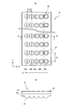
- FIG. 3 is a view showing a configuration example of a shadow mask and a microlens array used in the laser annealing apparatus according to the present invention.
- (A) is a plan view and (b) is a cross-sectional view taken along the line OO of (a).
- the shadow mask 21 is formed of chromium (Cr) or aluminum (deposited on a transparent quartz substrate 23 in order to determine the irradiation shape of the laser light L irradiated on the TFT substrate 5.
- the light shielding film 24 such as Al
- the shadow mask 21 has, for example, an arrangement pitch w of the gate electrodes 1 in a direction (Y direction) intersecting the transport direction (arrow A direction) of the TFT substrate 5. 1 , openings having the same opening area are arranged in a straight line. Moreover, the shadow mask 21 forms an opening 25a ⁇ 25e of different opening areas at the same pitch as the array pitch w 2 of the gate electrode 1 in the conveying direction in the same direction (X direction).
- openings having different opening areas are arranged with an arrangement pitch w in the transport direction.
- Two rows of 5 are provided.
- a group of openings 25a (hereinafter referred to as “opening row 26”) surrounded by an alternate long and short dash line shown in FIG. 3A forms one row.
- the other rows also have an opening row for each of the openings 25b to 25e.
- the opening area 25a of the opening located in the uppermost stream in the transport direction is formed so that the irradiation area of the laser light L that has passed through the opening is substantially equal to the plane area of the gate electrode 1, for example.
- the area 25e of the most downstream opening is the area of the channel region 10 in which the irradiation region of the laser light L that has passed through the opening is sandwiched between the source electrode 3 and the drain electrode 4 It is formed to be smaller than that.
- the opening area of each opening is the width in the same direction in the irradiation region of the laser light L that has passed through each opening without changing the width in the direction (Y direction) intersecting the conveying direction of each opening. Is substantially matched to the width of the gate electrode 1 in the same direction), and the width in the transport direction (X direction) is changed.
- the microlens array 22 includes a plurality of microlenses 27 capable of matching the optical axis at the center of each aperture, and the image of each aperture is reduced to an area corresponding to the gate electrode 1 to be focused. It has become.
- the alignment means 15 is for appropriately irradiating the target position with the laser light L. For example, when the TFT substrate 5 is transported while swinging left and right with respect to the transport direction, the TFT substrate The shadow mask 21 and the microlens array 22 are moved following the movement 5.
- the conveyance means 13 is provided with an imaging means 16 below the conveyance surface.
- the image pickup means 16 images the gate electrode 1 and the gate line 6 formed on the surface of the TFT substrate 5 through the back side of the TFT substrate 5.
- the imaging means 16 is, for example, a line camera having an elongated light receiving surface provided with a plurality of light receiving elements arranged in a straight line in a direction crossing the transport direction.
- the center line in the longitudinal direction of the light receiving surface of the line camera is matched with the center line of the opening row 26 located on the most upstream side in the transport direction (arrow A direction) of the shadow mask 21.
- the camera is arranged so as to photograph a position separated by a predetermined distance.
- the control device 17 comprehensively controls the transport unit 13, the laser irradiation optical system 14, the alignment unit 15, and the imaging unit 16. Note that the transport unit 13, the laser irradiation optical system 14, the alignment unit 15, the imaging unit 16, and the control device 17 are electrically connected.
- the control device 17 controls the change of the irradiation region of the laser light L by switching the opening of the shadow mask 21. Specifically, the control device 17 controls the irradiation amount of the laser light L because the laser annealing of the source region 11 and the drain region 12 is executed with a smaller irradiation amount of the laser light L than the laser annealing of the channel region 10. To do.
- control device 17 sets the crystal grain size of the polysilicon thin film 8 in the regions corresponding to the source electrode 3 and the drain electrode 4 of the TFT substrate 5 to the channel region 10 sandwiched between the source electrode 3 and the drain electrode 4.
- the crystal grain size of the polysilicon thin film 8 can be made smaller.
- the control device 17 sequentially moves the gate electrode 1 to be irradiated from the position immediately below the opening 25a in the shadow mask 21 to the position directly below the opening 25e each time the laser light L is irradiated.
- the control device 17 controls the amount of step movement so that the TFT substrate 5 is step-moved by the distance d (arrangement pitch w 2 ).
- the channel region 10 is multiply irradiated with the laser light L according to the opening. That is, in the channel region 10, the irradiation amount of the laser light L can be distributed.
- FIG. 4 is a block diagram showing an example of the configuration of the control means of the laser annealing apparatus according to the present invention.
- the control device 17 includes a transport unit drive controller 30, a laser drive controller 31, an alignment unit drive controller 32, an image processing unit 33, a calculation unit 34, a memory 35, and a control unit 36.
- the transport means drive controller 30 controls the drive of the transport means 13 so that the TFT substrate 5 is transported in the direction of arrow A at a predetermined constant speed.
- the laser drive controller 31 controls the drive of the laser 19 so that the laser light L is emitted at a predetermined time interval.
- the alignment means drive controller 32 controls the alignment means 15.
- the image processing unit 33 determines the edge (the boundary line in the Y direction of the gate electrode 1 (for example, 6 (a))) is detected as the first detection information, and extends in parallel to the transport direction from the luminance change in the direction intersecting the transport direction (luminance change in the major axis direction of the light receiving surface).
- the position of the edge of the gate line 6 (for example, e2 and e3 shown in FIG. 6A) is detected as second detection information.
- the image processing unit 33 outputs the first detection information, the second detection information, and the reference position information predetermined for the imaging unit 16 to the calculation unit 34.
- the calculation unit 34 inputs the first detection information and the second detection information from the image processing unit 33, and calculates the moving distance of the TFT substrate 5 from the detection time point. Subsequently, the arithmetic unit 34 opens a row of apertures located on the most upstream side in the transport direction of the shadow mask 21 with the transport of the TFT substrate 5 in order to match the travel distance of the TFT substrate 5 with the target value of the travel distance. It is determined whether or not the irradiation position of the laser beam L corresponding to the opening 25a of 26 matches the first irradiation position. If they match, the calculation unit 34 outputs a light emission command for one pulse (one shot) of the laser light L to the laser drive controller 31.
- the calculation unit 34 calculates the distance between the two based on the predetermined position information of the edge of the gate line 6 and the reference position information among the position information at the edge of the gate line 6 parallel to the transport direction. Then, a deviation amount between the distance and the alignment target value is calculated, and the deviation amount (positional deviation information) is output to the alignment means drive controller 32. Thereby, the alignment means drive controller 32 drives the alignment means 15 so as to correct the positional deviation based on the positional deviation information.
- the memory 35 is a rewritable storage device that stores the transport speed of the TFT substrate 5, the above-described target values, and the like.
- the control part 36 is provided with a processor, and controls the whole apparatus integrated so that said each element may operate
- the laser annealing apparatus 100 provides means that can reduce the leakage current when the TFT is turned off with a simple process by executing the steps of the laser annealing method described later based on the above configuration. it can.
- a method for manufacturing a TFT according to the present invention is a method for manufacturing a TFT having a gate electrode 1, a source electrode 3, a drain electrode 4 and a semiconductor layer 2 stacked on a TFT substrate 5, and is deposited on the TFT substrate 5.
- a step of a laser annealing method (hereinafter referred to as a “laser annealing step”) in which a region corresponding to the gate electrode 1 of the amorphous silicon thin film 7 is irradiated with a laser beam L to form a polysilicon thin film and the semiconductor layer 2 is formed. .
- the irradiation amount of the laser light L to the amorphous silicon thin film 7 in the regions corresponding to the source electrode 3 and the drain electrode 4 is smaller than the irradiation amount to the amorphous silicon thin film 7 in the channel region 10.
- multiple irradiation is performed by changing the irradiation region of the laser beam L.
- the irradiation region of the laser beam L is preferably changed by switching the opening of the shadow mask 21.
- the structure of the TFT manufactured by the TFT manufacturing method (for example, TFT 18 shown in FIG. 2) is basically the same as the structure of a known TFT except that the structure of the semiconductor layer 2 is different. Therefore, the conventional technique is applied to the basic manufacturing method. Therefore, here, the formation of the semiconductor layer 2 different from the prior art, particularly the laser annealing process will be described.
- the irradiation region of the laser beam L is changed and multiple irradiation is performed, and the crystal grain size of polysilicon is along at least the center line of the irradiation region of the laser beam L. A particle size distribution that decreases from the central portion toward the side end portion is generated.
- the opening of the shadow mask 21 is switched and multiple irradiation of the laser light L is executed. That is, in the laser annealing step, laser irradiation is executed in multiple stages on the predetermined channel region 10 by sequentially passing the laser light L through the plurality of openings 25a to 25e having different opening areas.
- the step movement amount of the irradiation position of the laser light L is set to the distance d.
- the amount is set to be equal to (arrangement pitch w 2 ).
- the distance d is also the width dimension of the channel region 10 in the transport direction.
- FIG. 5 is a cross-sectional view illustrating an example of a method for manufacturing a TFT according to the present invention.
- FIG. 6 is a plan view for explaining an example of a TFT manufacturing method according to the present invention.
- a case where laser annealing is performed by irradiation with five shots of laser light L will be described.
- the control device 17 moves the TFT substrate 5 in the direction of arrow A shown in FIG. 1 to position and stop at the first irradiation position described above.
- the control device 17 opens the opening area so that the irradiation shape of the laser light L onto the amorphous silicon thin film 7 is the same as that of the channel region 10.
- the amorphous silicon thin film 7 is irradiated with one shot of the laser beam L shaped by 25a toward the channel region 10 of the gate electrode 1 (first irradiation).
- FIG. 6A shows the center line C of the irradiation region of the laser light L.
- the control device 17 shows multiple irradiation as described below so as to produce a particle size distribution in which the crystal grain size of polysilicon decreases from the central portion toward the side end portion along the center line C of the irradiation region of the laser light L. To run.
- control device 17 changes the irradiation region of the laser light L to the previously irradiated polysilicon thin film 8 and performs the current irradiation, so that the TFT is aligned along the arrow direction shown in FIG.
- the substrate 5 is moved stepwise by the distance d, and the laser beam L shaped with the opening area 25b is irradiated by one shot in the same manner as described above (second irradiation, see FIGS. 5B and 6B). .
- the overlapping portion is crystallized by the current irradiation. (Crystal growth) is promoted.
- the crystal grain size of the polysilicon thin film 8 in the overlapping portion due to the current irradiation is larger than the crystal grain size of the polysilicon thin film 8 in the other part.
- the control device 17 changes the irradiation region of the laser light L to the previously irradiated polysilicon thin film 8 to step the TFT substrate 5 by a distance d in order to perform the current irradiation, and the same as described above.
- the laser beam L shaped with the opening area 25c is irradiated by one shot (third irradiation, see FIGS. 5C and 6C).
- the overlapping portion of the irradiation regions of the first to third shots of the laser light L is further increased because the irradiation amount of the laser light L is further increased than the irradiation amount of the two-shot laser light L.
- the crystallization of the partial polysilicon thin film 8 is further promoted. As a result, the crystal grain size of the polysilicon thin film 8 in the overlapping portion by this irradiation becomes larger.
- control device 17 changes the irradiation region of the laser beam L to the previously irradiated polysilicon thin film 8 to step the TFT substrate 5 by a distance d in order to perform the current irradiation, in the same manner as described above.
- the laser beam L shaped with the opening area 25d is irradiated by one shot (fourth irradiation, see FIGS. 5D and 6D).
- the overlapping area of the irradiation areas of the first to fourth shots of the laser light L is further increased than the irradiation quantity of the laser light L of the three shots.
- the crystallization of the partial polysilicon thin film 8 is further promoted.
- the crystal grain size of the polysilicon thin film 8 in the overlapping portion by this irradiation becomes larger.
- control device 17 changes the irradiation region of the laser beam L to the previously irradiated polysilicon thin film 8 and performs the final irradiation to move the TFT substrate 5 by a distance d in the same manner as described above. Then, the laser beam L shaped with the opening area 25e is irradiated by one shot (fifth irradiation, see FIGS. 5E and 6E).
- the laser annealing of the amorphous silicon thin film 7 in the region corresponding to the gate electrode 1 is finished, and the semiconductor layer 2 of the polysilicon thin film 8 is formed.
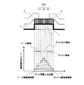
- FIG. 7 is an explanatory diagram showing the distribution of the laser beam irradiation amount in the TFT manufacturing method according to the present invention.
- the overlapping portion of the irradiation regions (the central portion of the channel region 10) with the first to fifth five-shot laser beams L has a four-shot laser beam L. Therefore, the crystallization (crystal growth) of the overlapping portion is further promoted. As a result, the crystal grain size of the polysilicon thin film 8 in the same part becomes larger.
- the crystal grain size of the polysilicon thin film 8 gradually decreases from the central portion of the channel region 10 toward the drain electrode 4 side end portion.
- the irradiation amount of the laser light L onto the amorphous silicon thin film 7 on the gate electrode 1 is moved as shown in FIG. Can have a distribution. That is, in the present embodiment, the amount of laser light L applied to the source region 11 and the drain region 12 can be reduced as compared with the channel region 10, and the progress of polysiliconization of the source region 11 and the drain region 12 can be controlled. 10 or less. Thereby, in this embodiment, the crystal grain size of the polysilicon thin film 8 in the source region 11 and the drain region 12 can be made smaller than the crystal grain size of the polysilicon thin film 8 in the channel region 10.
- the number of shots n of the laser beam L required for laser annealing is preferably determined so that irradiation energy sufficient to melt at least the entire thickness of the amorphous silicon thin film 7 in the channel region 10 can be obtained.
- the processing for reducing the crystal grain size of the polysilicon thin film 8 in the source region 11 and the drain region 12 as compared with the crystal grain size of the polysilicon thin film 8 in the channel region 10 is performed.
- the applied TFT 18 can be manufactured by a simple process. Therefore, the TFT 18 subjected to such processing can make the electron mobility of the source region 11 and the drain region 12 of the semiconductor layer 2 lower than the electron mobility of the channel region 10, and the leakage current when the TFT is turned off can be reduced. Can be reduced.
- the minimum irradiation region of the laser beam L is preferably smaller than the plane area of the channel region 10, and it is preferable that the minimum irradiation region is irradiated with laser (multiple irradiation) as many times as possible.
- the irradiation region of the laser light L can be changed by switching the opening of the shadow mask 21 to perform multiple irradiation, and the distribution of the crystal grain size of the polysilicon thin film 8 in the channel region 10 can be easily performed. Can be controlled.
- the laser annealing method of the present invention including the laser annealing step will be described in more detail.
- a case where the laser light L is executed in five shots as laser annealing will be described by paying attention to one gate electrode 1.
- the transport means 13 is controlled by the control device 17 to start transporting the TFT substrate 5 in the direction of arrow A shown in FIG.
- the gate electrode 1 and the gate line 6 formed on the front surface of the TFT substrate 5 through the TFT substrate 5 are photographed by the imaging means 16 from the back side of the TFT substrate 5.
- an image photographed by the imaging unit 16 is processed by the image processing unit 33, and the moving distance of the TFT substrate 5 is calculated by the calculation unit 34.
- the control unit 36 matches the target value of the movement distance stored in the memory 35 and the laser corresponding to the opening 25a of the opening row 26 located on the most upstream side in the transport direction of the shadow mask 21. Control is performed so that the irradiation position of the light L matches a predetermined initial irradiation position of the end region on the source electrode 3 side on the gate electrode 1.
- the calculation unit 34 outputs the position shift information to the alignment means drive controller 32 when the position shift occurs.
- the alignment means drive controller 32 drives the alignment means 15 so as to correct the positional deviation based on the positional deviation information, and finely moves the shadow mask 21 and the microlens array 22 integrally in a direction crossing the transport direction.
- the shadow mask 21 and the microlens array 22 move following the movement of the TFT substrate 5 in the direction intersecting the conveyance direction, and appropriately irradiate the laser beam L to a predetermined position on the gate electrode 1. be able to.
- the tracking operation of the shadow mask 21 and the microlens array 22 with respect to the TFT substrate 5 is always performed while the TFT substrate 5 is being transported.
- the calculation unit 34 outputs a light emission command for one pulse of the laser beam L to the laser drive controller 31.
- the laser drive controller 31 drives the laser 19 based on the light emission command input from the calculation unit 34 and emits one pulse of the laser light L.
- the laser beam L emitted by the laser 19 is irradiated with a shadow mask 21 with a beam diameter expanded by a coupling optical system 20 and a uniform luminance distribution.
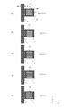
- FIG. 8 is an explanatory diagram showing the operation of the laser annealing method according to the present invention.
- the laser beam L irradiated to the shadow mask 21 is separated into a plurality of laser beams L by a plurality of aperture groups provided in the shadow mask 21. Further, as shown in FIG. 8A, the separated laser beams L are first directed toward the amorphous silicon thin film 7 on the gate electrode 1 by the microlenses 27 provided corresponding to the respective openings. It is condensed at the irradiation position. At this time, on the amorphous silicon thin film 7, the image of the opening 25a is reduced and projected, and the region having the same shape as the channel region 10 is illuminated by the laser light L.
- the amorphous silicon thin film 7 at the first irradiation position irradiated with the laser light L of the first shot is instantaneously heated and melted, and a part of the amorphous silicon thin film 7 is turned into polysilicon (polycrystalline).
- the moving distance of the TFT substrate 5 is calculated. Then, the movement distance of the TFT substrate 5 is moved by a distance d equal to the arrangement pitch w 2 in the conveyance direction of the gate electrodes 1 stored in the memory 35, and the gate electrode 1 is moved in the conveyance direction as shown in FIG.
- the laser drive controller 31 drives the laser 19 to emit the second shot of laser light L.
- the laser light L of the second shot is focused on the amorphous silicon thin film 7 on the gate electrode 1 by the microlens 27 as shown in FIG. Then, due to the second shot of laser light L, the crystal grain size of the polysilicon thin film 8 in the overlapping portion due to the current irradiation becomes larger than the crystal grain size of the polysilicon thin film 8 in the other part. That is, the irradiation energy higher than the irradiation region of the first-shot laser beam L is given to the overlapping portion of the irradiation region of the first-shot laser beam L and the irradiation region of the second-shot laser beam L, Crystallization of the polysilicon thin film 8 in the same portion is promoted.
- the laser beam L is emitted every time the TFT substrate 5 is transported by the distance d, and the third to fifth shots of the laser beam L are applied to the gate electrode 1.
- the polysilicon thin film 8 is irradiated.
- the irradiation amount of the laser beam L increases as the number of overlapping of the irradiation regions increases. Growth) is further promoted. As a result, the crystal grain size of the polysilicon thin film 8 in the channel region 10 where the irradiation amount of the laser beam L is large is larger than the crystal grain size of the polysilicon thin film 8 in the source region 11 and the drain region 12 where the irradiation amount of the laser beam L is small. growing.
- FIG. 9 is a view showing a configuration example of a shadow mask used in the laser annealing apparatus according to the present invention.
- the shadow mask 21a shown in FIG. 9 is formed so that the width in the transport direction is not changed by changing the width in the direction intersecting the transport direction of each opening so that the longitudinal direction of each opening coincides with the transport direction. Yes.
- the width of each opening in the direction intersecting the transport direction is formed so as to gradually decrease toward the downstream in the transport direction.
- this shadow mask 21a may be employed to manufacture a TFT.
- FIG. 10 is a plan view for explaining an example of a TFT manufacturing method according to the present invention.
- laser annealing is performed by irradiating five shots of laser light L as an example in the same manner as the TFT manufacturing method shown in FIG.
- the source electrode 3, the channel region 10 and the drain electrode 4 are arranged so that the arrangement of the TFT substrate 5 is 90 degrees clockwise so that the particle size distribution by the TFT manufacturing method shown in FIG. Are arranged so as to intersect the transport direction (arrow A direction).
- the image processing unit 33 detects the edge in the transport direction of the gate electrode 1 (the boundary line in the X direction of the gate electrode 1) from the luminance change in the transport direction based on the image information captured by the imaging unit 16. (For example, the line e4 shown in FIG. 10)) is detected as the first detection information, and the edge of the gate line 6 extending perpendicularly to the transport direction from the luminance change in the transport direction (for example, in FIG. 10). The positions indicated by e2 and e3) are detected as second detection information.
- the irradiation position accuracy in the transport direction (X direction) is shifted to the left and right (X direction) by 1 micron or more in some cases due to the time delay of the laser oscillation with respect to the light emission command from the laser drive controller 31.
- the alignment means drive controller 32 can control the irradiation accuracy in the direction (Y direction) intersecting the transport direction to the order of submicrons. Therefore, according to the TFT manufacturing method shown in FIG. 10, laser annealing can be performed by correcting the positional deviation of the center line C with high accuracy to further increase the irradiation accuracy.
- the distribution of the crystal grain size of the polysilicon thin film 8 may be formed so that the leakage current when the TFT is turned off can be reduced. It is not limited to performing annealing.
- the irradiation width of the laser light L is gradually reduced as shown in FIG. 6A.
- the shadow mask 21 shown in FIG. thus, the laser beam L may be irradiated in such a manner that the irradiation width is increased stepwise.
Landscapes
- Recrystallisation Techniques (AREA)
- Physics & Mathematics (AREA)
- Optics & Photonics (AREA)
- Thin Film Transistor (AREA)
- Electromagnetism (AREA)
- Chemical & Material Sciences (AREA)
- Crystallography & Structural Chemistry (AREA)
Abstract
本発明は、基板(5)上に被着されたアモルファスシリコン薄膜7にレーザ光Lを照射してポリシリコン化するレーザアニール方法であって、前記アモルファスシリコン薄膜7上への前記レーザ光Lの照射領域を変更して多重照射し、ポリシリコンの結晶粒径が前記レーザ光Lの照射領域の少なくとも中心線Cに沿って中央部から側端部に向かって小さくなる粒径分布を生じさせる。これにより、簡単なプロセスでリーク電流を低減可能なレーザアニール方法を実現できる。
Description
本発明は、アモルファスシリコン薄膜のレーザアニール方法に関し、特に薄膜トランジスタにおけるリーク電流の低減化を可能とするレーザアニール方法、レーザアニール装置及び薄膜トランジスタの製造方法に係るものである。
一般に、薄膜トランジスタ(Thin Film Transistor:以下「TFT」という)は、ゲート電極、ソース電極、ドレイン電極及び半導体層を積層して備えた構造を有している。この場合、半導体層としてポリシリコン薄膜を用いたTFTは、電子の移動度が高く、低消費電力のディスプレイに用いられている。従来から、TFT基板の製造工程において、例えば、レーザアニール法により、TFT基板に成膜されたアモルファスシリコンを結晶化させ、ポリシリコン(多結晶シリコン)膜にすることが知られている(例えば、特許文献1参照)。
しかし、従来、TFT基板のレーザアニール処理では、例えば、TFT基板の全面を紫外線のレーザ光を照射することにより、均一にアニール処理することが行われている。この場合、ソース電極、ドレイン電極下の領域にもポリシリコン膜が形成されるため、電極間の電界強度がその分、高くなり、いわゆるTFTオフ時のリーク電流(オフ電流)を低減することが困難であるという問題点を有している。この問題点を解消するため、例えば、LDD(Lightly Doped Drain)構造が採用されているものの、製造工程が複雑になり、コストも増加する。
そこで、このような問題点に対処し、本発明が解決しようとする課題は、簡単なプロセスでリーク電流の低減可能なレーザアニール方法、レーザアニール装置及びTFTの製造方法を提供することにある。
上記目的を達成するために、本発明によるレーザアニール方法は、基板上に被着されたアモルファスシリコン薄膜にレーザ光を照射してポリシリコン化するレーザアニール方法であって、前記アモルファスシリコン薄膜上への前記レーザ光の照射領域を変更して多重照射し、ポリシリコンの結晶粒径が前記レーザ光の照射領域の少なくとも中心線に沿って中央部から側端部に向かって小さくなる粒径分布を生じさせる。
また、本発明によるレーザアニール装置は、基板上のゲート電極に対応した領域のアモルファスシリコン薄膜をレーザアニールにより、TFTの半導体層を形成するレーザアニール装置であって、ソース電極及びドレイン電極に夫々対応した領域の前記アモルファスシリコン薄膜へのレーザ光の照射量を、前記ソース電極と前記ドレイン電極とに挟まれたチャンネル領域の前記アモルファスシリコン薄膜への照射量よりも少なくなるように、前記レーザ光の照射領域を変えて多重照射させる光学系と、前記光学系における前記レーザ光の照射領域の変更を制御する制御手段と、を備えたものである。
また、本発明によるTFTの製造方法は、基板上にゲート電極、ソース電極、ドレイン電極及び半導体層を積層して備えた薄膜トランジスタの製造方法であって、前記基板上に被着されたアモルファスシリコン薄膜の前記ゲート電極に対応した領域にレーザ光を照射してポリシリコン薄膜とすることにより、前記半導体層を形成するレーザアニール方法の工程を含み、
前記工程は、前記ソース電極及び前記ドレイン電極に夫々対応した領域の前記アモルファスシリコン薄膜へのレーザ光の照射量を、前記ソース電極と前記ドレイン電極とに挟まれたチャンネル領域の前記アモルファスシリコン薄膜への照射量よりも少なくなるように、前記レーザ光の照射領域を変えて多重照射して実行する。
前記工程は、前記ソース電極及び前記ドレイン電極に夫々対応した領域の前記アモルファスシリコン薄膜へのレーザ光の照射量を、前記ソース電極と前記ドレイン電極とに挟まれたチャンネル領域の前記アモルファスシリコン薄膜への照射量よりも少なくなるように、前記レーザ光の照射領域を変えて多重照射して実行する。
本発明によれば、アモルファスシリコン薄膜上へのレーザ光の照射領域を変更して多重照射するという簡単なプロセスを実行することにより、ポリシリコンの結晶粒径がレーザ光の照射領域の少なくとも中心線に沿って中央部から側端部に向かって小さくなる粒径分布を生じるようにすることができる。
したがって、上記の粒径分布により、中央部から側端部に向かって結晶化率が抑制されることに伴い、抵抗が上昇するのでリーク電流を低減することができる。
したがって、上記の粒径分布により、中央部から側端部に向かって結晶化率が抑制されることに伴い、抵抗が上昇するのでリーク電流を低減することができる。
以下、本発明の実施形態を添付図面に基づいて詳細に説明する。
図1は、本発明によるレーザアニール装置の一実施形態を示す概要図である。図2は、本発明によるレーザアニール装置で成膜されるTFTの一実施形態を示す断面図である。図1に示すレーザアニール装置100は、TFT基板5上のゲート電極に対応した領域のアモルファスシリコン薄膜をレーザアニールにより、TFT18の半導体層を形成するものである。
図1は、本発明によるレーザアニール装置の一実施形態を示す概要図である。図2は、本発明によるレーザアニール装置で成膜されるTFTの一実施形態を示す断面図である。図1に示すレーザアニール装置100は、TFT基板5上のゲート電極に対応した領域のアモルファスシリコン薄膜をレーザアニールにより、TFT18の半導体層を形成するものである。
具体的には、レーザアニール装置100は、搬送手段13と、レーザ照射光学系14と、アライメント手段15と、撮像手段16と、制御装置17と、を備える。なお、レーザ照射光学系14は光学系の一例であり、制御装置17は制御手段の一例である。また、TFT基板5は、本実施形態に適用される基板の一例であって、複数のデータ線及びゲート線を縦横に交差させることにより設けられた交差部(図示省略)にTFT18のゲート電極を設けたものである。
搬送手段13は、最表面にアモルファスシリコン薄膜が形成されたTFT基板5を所定の方向に搬送するものであり、例えば、ゲート線と搬送方向(矢印A方向)とが平行となるようにTFT基板5を位置決めして載置できるようになっている。
ここで、各TFT18は、図2に示す通り、ディスプレイの画素電極を駆動するためのものであって、ゲート電極1と、半導体層2と、ソース電極3と、ドレイン電極4と、を備える。
ゲート電極1は、例えば、透明ガラスから成るTFT基板5上に一定の配列ピッチでマトリクス状に複数形成されたもので、TFT基板5の横方向に平行に伸びて形成された複数のゲート線6(図6参照)に電気的に接続され、表示領域外に設けられたゲートドライブ回路から走査情報が供給されるようになっている。
また、ゲート電極1を覆って、半導体層2が設けられている。本実施形態における半導体層2は、TFT基板5上に被着されたアモルファスシリコン薄膜7の少なくともゲート電極1に対応した領域に紫外線のレーザ光L(図1参照)が照射されることにより、アモルファスシリコン薄膜7がレーザアニールにより形成されたポリシリコン薄膜8を含む。なお、半導体層2とゲート電極1との間には、絶縁膜9が設けられている。そして、ソース電極3及びドレイン電極4に夫々対応した領域のポリシリコン薄膜8の結晶粒径は、ソース電極3とドレイン電極4とに挟まれたチャンネル領域10のポリシリコン薄膜8の結晶粒径に比べて小さくした構造を有している。
つまり、半導体層2は、一例として、ソース電極3及びドレイン電極4に夫々対応した領域のアモルファスシリコン薄膜7へのレーザ光Lの照射量がチャンネル領域10のアモルファスシリコン薄膜7への照射量よりも少なくなるようにして形成されている。以下、ソース電極3に対応した半導体層2の領域を「ソース領域11」といい、ドレイン電極4に対応した半導体層2の領域を「ドレイン領域12」という。
また、半導体層2において、ゲート電極1の一方端側には、ソース電極3が設けられている。このソース電極3は、ゲート線6に交差させて設けられた図示省略のデータ線に電気的に接続されており、表示領域外に設けられたソースドライブ回路からデータ信号が供給されるようになっている。
さらに、半導体層2において、ゲート電極1の他方端側には、ドレイン電極4が設けられている。このドレイン電極4は、図示省略のディスプレイの画素電極にデータ線及びソース電極3を介して供給されるデータ信号を供給するものであって、この画素電極に電気的に接続させて設けられている。そして、ソース電極3及びドレイン電極4上には、絶縁膜9からなる図示省略の保護膜が形成されている。
図1に戻り、搬送手段13の上方には、レーザ照射光学系14が配設されている。このレーザ照射光学系14は、TFT基板5のアモルファスシリコン薄膜7上へレーザ光Lを照射するものである。詳細には、レーザ照射光学系14は、図2に示すTFT18のソース電極3及びドレイン電極4に夫々対応した領域のアモルファスシリコン薄膜7へのレーザ光Lの照射量を、ソース電極3とドレイン電極4とに挟まれたチャンネル領域10のアモルファスシリコン薄膜7への照射量よりも少なくなるように、レーザ光Lの照射領域を変えて多重照射させる。つまり、レーザ照射光学系14は、ゲート電極1上のアモルファスシリコン薄膜7をポリシリコン化して半導体層2を形成することができる。
ここで、レーザ照射光学系14は、レーザ19と、そのレーザ19が放出するレーザ光Lの進行方向の順に、カップリング光学系20と、シャドウマスク21と、マイクロレンズアレイ22と、を備える。レーザ19は、紫外線のレーザ光Lをパルス発光するもので、例えば、波長が355nmのYAG(Yttrium Aluminum Garnet)レーザや、例えば、波長が308nmのエキシマレーザである。
また、カップリング光学系20は、レーザ19から放出されたレーザ光Lを拡張すると共に均一化してシャドウマスク21に照射させるものであり、例えば、図示省略のビームエキスパンダ、フォトインテグレータ、コリメータレンズ等の光学機器を含む。
さらに、シャドウマスク21は、開口面積の異なる複数の開口を有し、1つのレーザ光Lから複数のレーザ光Lに分離するものである。これにより、本実施形態では、レーザ光Lの多重照射を容易にすることができる。
図3は、本発明によるレーザアニール装置に使用するシャドウマスク及びマイクロレンズアレイの一構成例を示す図である。(a)は平面図、(b)は(a)のO-O線断面矢視図である。シャドウマスク21は、図3(b)に示す通り、TFT基板5上に照射されるレーザ光Lの照射形状を決めるため、透明な石英基板23上に成膜されたクロム(Cr)又はアルミニウム(Al)等の遮光膜24に開口面積の異なる複数の開口を有している。
詳細には、シャドウマスク21は、図3(a)に示すように、一例として、TFT基板5の搬送方向(矢印A方向)と交差する方向(Y方向)に、ゲート電極1の配列ピッチw1で同じ開口面積の開口を一直線に並べて形成している。また、シャドウマスク21は、上記搬送方向と同方向(X方向)のゲート電極1の配列ピッチw2と同じピッチで異なる開口面積の開口25a~25eを形成している。
より詳細には、レーザアニールがレーザ光Lのn回ショット(nは正の整数)で行われる場合、一例として、n=5とすると、開口面積の異なる開口は、上記搬送方向に配列ピッチw2で5列設けられる。例えば、図3(a)に示す一点鎖線で囲まれた開口25a群(以下「開口列26」という)が、1つの列を形成している。なお、他の列も各々同様に開口25b~25e毎に開口列を形成している。さらに、搬送方向の最上流に位置する開口の開口面積25aは、該開口を通過したレーザ光Lの照射領域が例えばゲート電極1の平面積に略等しくなるように形成され、各開口の開口面積は搬送方向下流に向かって漸減して、最下流の開口の面積25eは、該開口を通過したレーザ光Lの照射領域がソース電極3とドレイン電極4とに挟まれたチャンネル領域10の平面積よりも小さくなるように形成されている。
なお、本実施形態において、各開口の開口面積は、各開口の搬送方向と交差する方向(Y方向)の幅は変えずに(各開口を通過したレーザ光Lの照射領域における同方向の幅がゲート電極1の同方向の幅に略合致するようにし)、搬送方向(X方向)の幅を変えて変化させている。
マイクロレンズアレイ22は、上記各開口の中心に光軸を合致可能な複数のマイクロレンズ27を備えたものであり、各開口の像をゲート電極1に対応した領域に縮小して合焦させるようになっている。
図1に戻り、アライメント手段15は、レーザ光Lを目標位置に適切に照射させるためのものであり、例えば、TFT基板5が搬送方向に対して左右に振れながら搬送された場合、そのTFT基板5の動きに追従させてシャドウマスク21及びマイクロレンズアレイ22を移動させる。
搬送手段13は、搬送面の下側に撮像手段16を設けている。この撮像手段16は、TFT基板5の裏面側から透かして、そのTFT基板5の表面に形成されたゲート電極1及びゲート線6を撮影するものである。撮像手段16は、例えば、複数の受光素子を搬送方向と交差する方向に一直線に並べて備えた細長状の受光面を有するラインカメラである。そして、このラインカメラは、例えば、シャドウマスク21の搬送方向(矢印A方向)の最も上流側に位置する開口列26の中心線に、ラインカメラの受光面の長手方向の中心線を合致させることにより、予め定められた所定距離だけ離れた位置を撮影するように配置されている。
制御装置17は、搬送手段13、レーザ照射光学系14、アライメント手段15及び撮像手段16を統括的に制御する。なお、搬送手段13、レーザ照射光学系14、アライメント手段15、撮像手段16及び制御装置17は、電気的に接続されている。この制御装置17は、シャドウマスク21の開口を切替えることにより、レーザ光Lの照射領域の変更を制御する。具体的には、制御装置17は、ソース領域11及びドレイン領域12のレーザアニールを、チャンネル領域10のレーザアニールよりも少ないレーザ光Lの照射量で実行するため、レーザ光Lの照射量を制御するものである。これにより、制御装置17は、TFT基板5のソース電極3及びドレイン電極4に夫々対応した領域のポリシリコン薄膜8の結晶粒径を、ソース電極3とドレイン電極4とに挟まれたチャンネル領域10のポリシリコン薄膜8の結晶粒径に比べて小さくすることができる。
詳細には、制御装置17は、当該照射対象となるゲート電極1を、シャドウマスク21における開口25aの直下の位置から開口25eの直下の位置へと、レーザ光Lを照射する毎に順番に移動させる。換言すると、制御装置17は、距離d(配列ピッチw2)でTFT基板5をステップ移動するようにステップ移動量を制御するものである。これにより、チャンネル領域10が開口に応じてレーザ光Lで多重照射される。つまり、チャンネル領域10において、レーザ光Lの照射量に分布を持たせることができる。
図4は、本発明によるレーザアニール装置の制御手段の一構成例を示すブロック図である。制御装置17は、搬送手段駆動コントローラ30と、レーザ駆動コントローラ31と、アライメント手段駆動コントローラ32と、画像処理部33と、演算部34と、メモリ35と、制御部36と、を備える。
ここで、搬送手段駆動コントローラ30は、TFT基板5を予め定められた一定速度で矢印A方向に搬送させるように搬送手段13の駆動を制御するものである。また、レーザ駆動コントローラ31は、レーザ光Lを所定の時間間隔でパルス発光させるようにレーザ19の駆動を制御するものである。さらに、アライメント手段駆動コントローラ32は、上記アライメント手段15を制御するものである。
画像処理部33は、上記撮像手段16により撮影された画像情報に基づいて搬送方向の輝度変化から、ゲート電極1の搬送方向と交差する縁部(ゲート電極1のY方向の境界線(例えば、図6(a)に示すe1のライン))を第1の検出情報として検出すると共に、搬送方向と交差する方向の輝度変化(受光面の長軸方向の輝度変化)から搬送方向に平行に伸びるゲート線6の縁部(例えば、図6(a)に示すe2とe3)の位置を第2の検出情報として検出する。これにより、画像処理部33は、第1の検出情報と、第2の検出情報と、撮像手段16に予め定められた基準位置情報とを演算部34に出力する。
演算部34は、先ず、第1の検出情報と、第2の検出情報とを画像処理部33から入力し、該検出時点からTFT基板5の移動距離を演算する。続いて、演算部34は、TFT基板5の移動距離と移動距離の目標値とを合致させるべく、TFT基板5の搬送に伴って、シャドウマスク21の搬送方向の最も上流側に位置する開口列26の開口25aに対応するレーザ光Lの照射位置が最初の照射位置に合致するか否かを判定する。合致した場合、演算部34は、レーザ駆動コントローラ31に1パルス(1ショット)のレーザ光Lの発光指令を出力するようになっている。
また、演算部34は、搬送方向に平行なゲート線6の縁部における位置情報のうち予め定められたゲート線6の縁部の位置情報と基準位置情報とに基づいて両者間の距離を演算し、該距離とアライメント目標値とのずれ量を算出し、そのずれ量(位置ずれ情報)をアライメント手段駆動コントローラ32に出力するようになっている。これにより、アライメント手段駆動コントローラ32は、上記位置ずれ情報に基づいて位置ずれを補正するようにアライメント手段15を駆動することになる。
メモリ35は、TFT基板5の搬送速度、上記各目標値等を保存するものであり、書き換え可能な記憶装置である。そして、制御部36は、プロセッサを備え、上記各要素が適切に動作するように装置全体を統合して制御するものである。
以上より、レーザアニール装置100は、上記の構成に基づいて、後述するレーザアニール方法の工程を実行することで、簡単なプロセスで、TFTオフ時のリーク電流の低減化を可能とする手段を提供できる。
次に、上記レーザアニール装置100を用いたTFTの製造方法について説明する。本発明によるTFTの製造方法は、TFT基板5上にゲート電極1、ソース電極3、ドレイン電極4及び半導体層2を積層して備えたTFTの製造方法であって、TFT基板5上に被着されたアモルファスシリコン薄膜7のゲート電極1に対応した領域にレーザ光Lを照射してポリシリコン薄膜とし、半導体層2を形成するレーザアニール方法の工程(以下、「レーザアニール工程」という)を含む。
そして、レーザアニール工程は、ソース電極3及びドレイン電極4に夫々対応した領域のアモルファスシリコン薄膜7へのレーザ光Lの照射量がチャンネル領域10のアモルファスシリコン薄膜7への照射量よりも少なくなるように、レーザ光Lの照射領域を変えて多重照射して実行される。ここで、レーザ光Lの照射領域の変更は、シャドウマスク21の開口を切替えて行われることが好ましい。
なお、TFTの製造方法で製造するTFTの構造(例えば、図2に示すTFT18)は、半導体層2の構造が異なる点を除いて公知のTFTの構造と基本的に同様である。そのため、基本的な製造方法は、従来技術が適用される。そこで、ここでは、従来技術と異なる半導体層2の形成、特にレーザアニール工程について説明する。
また、TFTの製造方法におけるレーザアニール工程は、上述した通り、レーザ光Lの照射領域を変更して多重照射し、ポリシリコンの結晶粒径がレーザ光Lの照射領域の少なくとも中心線に沿って中央部から側端部に向かって小さくなる粒径分布を生じるようにする。
一例として、レーザアニール工程では、TFT基板5をステップ移動させる毎に、シャドウマスク21の開口を切替えて、レーザ光Lの多重照射が実行される。つまり、レーザアニール工程では、レーザ光Lを開口面積の異なる複数の開口25a~25eに順番に通過させることにより、所定のチャンネル領域10に対して多段階にレーザ照射が実行される。
より詳細には、上記レーザアニール工程では、レーザアニールをレーザ光Lのnショット(nは、例えば3以上の整数)で実行する場合に、上記レーザ光Lの照射位置のステップ移動量を距離d(配列ピッチw2)に等しい量となるように設定する。なお、距離dは、チャンネル領域10の搬送方向の幅寸法でもある。
以下、レーザアニール工程を、図5及び図6を参照して説明する。レーザとしては、例えば、YAGレーザを使用する。
図5は、本発明によるTFTの製造方法の一例を説明する断面図である。図6は、本発明によるTFTの製造方法の一例を説明する平面図である。ここでは、一例として5ショットのレーザ光Lの照射によりレーザアニールが実行される場合について説明する。
図5は、本発明によるTFTの製造方法の一例を説明する断面図である。図6は、本発明によるTFTの製造方法の一例を説明する平面図である。ここでは、一例として5ショットのレーザ光Lの照射によりレーザアニールが実行される場合について説明する。
制御装置17は、先ず、図1に示す矢印A方向にTFT基板5を移動させて、上述した、最初の照射位置に位置決めして停止させる。次に、制御装置17は、図5(a)及び図6(a)に示すように、アモルファスシリコン薄膜7上へのレーザ光Lの照射形状がチャンネル領域10と同じ形状となるように開口面積25aで整形されたレーザ光Lを、ゲート電極1のチャンネル領域10に向けて、アモルファスシリコン薄膜7に1ショット照射させる(1回目の照射)。これにより、アモルファスシリコン薄膜7のレーザ光Lの照射された部分が瞬間加熱されて溶融し、シリコン分子の結合状態がアモルファス(非結晶)状態から、ポリ(多結晶)状態に変えられてポリシリコン薄膜8となる。なお、図6(a)にレーザ光Lの照射領域の中心線Cを示す。制御装置17は、ポリシリコンの結晶粒径がレーザ光Lの照射領域の中心線Cに沿って中央部から側端部に向かって小さくなる粒径分布を生じるように多重照射を以下に示すように実行する。
次に、制御装置17は、前回照射したポリシリコン薄膜8に対し、レーザ光Lの照射領域を変更して、今回の照射をするため、図3(a)に示す矢印方向に沿って、TFT基板5を距離dだけステップ移動させ、上記と同様にして、開口面積25bで整形されたレーザ光Lを1ショット照射させる(2回目の照射、図5(b)及び図6(b)参照)。
これにより、1回目のレーザ光Lの照射領域と2回目の照射領域との重なり部分は、1回目の照射領域よりもレーザ光Lの照射量が増すので、今回の照射による重なり部分の結晶化(結晶成長)が促進される。その結果、今回の照射による重なり部分のポリシリコン薄膜8の結晶粒径は、他の部分におけるポリシリコン薄膜8の結晶粒径に比べて大きくなる。
次に、制御装置17は、前回照射したポリシリコン薄膜8に対し、レーザ光Lの照射領域を変更して、今回の照射をするため、TFT基板5を距離dだけステップ移動させ、上記と同様にして、開口面積25cで整形されたレーザ光Lを1ショット照射させる(3回目の照射、図5(c)及び図6(c)参照)。
これにより、1回目~3回目の3ショットのレーザ光Lによる照射領域の重なり部分は、レーザ光Lの照射量が2ショットのレーザ光Lの照射量よりもさらに増すので、今回の照射による重なり部分のポリシリコン薄膜8の結晶化はより促進される。その結果、今回の照射による重なり部分のポリシリコン薄膜8の結晶粒径は、より大きくなる。
さらに、制御装置17は、前回照射したポリシリコン薄膜8に対し、レーザ光Lの照射領域を変更して、今回の照射をするため、TFT基板5を距離dだけステップ移動させ、上記と同様にして、開口面積25dで整形されたレーザ光Lを1ショット照射させる(4回目の照射、図5(d)及び図6(d)参照)。
これにより、1回目~4回目の4ショットのレーザ光Lによる照射領域の重なり部分は、レーザ光Lの照射量が3ショットのレーザ光Lの照射量よりもさらに増すので、今回の照射による重なり部分のポリシリコン薄膜8の結晶化はさらに促進される。その結果、今回の照射による重なり部分のポリシリコン薄膜8の結晶粒径は、より大きくなる。
さらにまた、制御装置17は、前回照射したポリシリコン薄膜8に対し、レーザ光Lの照射領域を変更して、最後の照射をするため、TFT基板5を距離dだけステップ移動させ、上記と同様にして、開口面積25eで整形されたレーザ光Lを1ショット照射させる(5回目の照射、図5(e)及び図6(e)参照)。
これにより、ゲート電極1に対応した領域のアモルファスシリコン薄膜7のレーザアニールが終了し、ポリシリコン薄膜8の半導体層2が形成される。
図7は、本発明によるTFTの製造方法におけるレーザ光の照射量の分布を示す説明図である。図7に示す通り、1回目~5回目の5ショットのレーザ光Lによる照射領域の重なり部分(チャンネル領域10の中央部)は、5ショットのレーザ光Lの照射量が4ショットのレーザ光Lの照射量よりもさらに増すので、上記重なり部分の結晶化(結晶成長)は、より促進される。その結果、同部分のポリシリコン薄膜8の結晶粒径は、より大きくなる。
また、チャンネル領域10の中央部からドレイン電極4側端部に向かって、レーザ光Lの照射領域の重なる回数が減るためレーザ光Lの照射量が減少する。したがって、チャンネル領域10の中央部からドレイン電極4側端部に向かって、ポリシリコン薄膜8の結晶粒径が次第に小さくなる。
上述したように、本実施形態では、レーザ光Lの照射位置を距離dずつステップ移動させることにより、図7に示すように、ゲート電極1上のアモルファスシリコン薄膜7へのレーザ光Lの照射量に分布を持たせることができる。即ち、本実施形態では、チャンネル領域10に比べてソース領域11及びドレイン領域12のレーザ光Lの照射量を少なくすることができ、ソース領域11及びドレイン領域12のポリシリコン化の進行をチャンネル領域10よりも抑えることができる。これにより、本実施形態では、ソース領域11及びドレイン領域12のポリシリコン薄膜8の結晶粒径をチャンネル領域10のポリシリコン薄膜8の結晶粒径に比べて小さくすることができる。
なお、レーザアニールに要するレーザ光Lのショット回数nは、少なくともチャンネル領域10におけるアモルファスシリコン薄膜7の全膜厚を溶融させるのに十分な照射エネルギーが得られるように決定するのがよい。
以上より、本発明のTFTの製造方法によれば、ソース領域11及びドレイン領域12のポリシリコン薄膜8の結晶粒径をチャンネル領域10のポリシリコン薄膜8の結晶粒径に比べて小さくする加工を施したTFT18を簡単なプロセスで製造することができる。したがって、このような加工を施したTFT18は、半導体層2のソース領域11及びドレイン領域12の電子移動度をチャンネル領域10の電子移動度よりも低くすることができ、TFTオフ時のリーク電流を低減することができる。
なお、レーザ光Lの最小照射領域は、上記の通り、チャンネル領域10の平面積よりも小さくすることが好ましく、その最小照射領域が最も多い回数でレーザ照射(多重照射)されることが好ましい。本実施形態では、レーザ光Lの照射領域の変更を、シャドウマスク21の開口を切替えて行うことにより、多重照射することができ、容易にチャンネル領域10におけるポリシリコン薄膜8の結晶粒径の分布を制御することができる。
次に、上記レーザアニール工程を含む、本発明のレーザアニール方法について、さらに詳細に説明する。ここでは、1つのゲート電極1に注目し、レーザアニールとして、レーザ光Lが5ショットで実行される場合について説明する。
先ず、搬送手段13が制御装置17によって制御されて、TFT基板5を図1に示す矢印A方向に一定速度で搬送を開始する。
先ず、搬送手段13が制御装置17によって制御されて、TFT基板5を図1に示す矢印A方向に一定速度で搬送を開始する。
次に、撮像手段16によりTFT基板5の裏面側からTFT基板5を透かして表面に形成されたゲート電極1及びゲート線6が撮影される。この場合、撮像手段16により撮影された画像が画像処理部33で処理され、TFT基板5の移動距離が演算部34において演算される。そして、制御部36は、その移動距離がメモリ35に保存された移動距離の目標値に合致して、シャドウマスク21の搬送方向の最も上流側に位置する開口列26の開口25aに対応するレーザ光Lの照射位置がゲート電極1上のソース電極3側端部領域の予め定められた最初の照射位置に合致させるように制御する。
この際、演算部34では、位置ずれが生じた場合、位置ずれ情報をアライメント手段駆動コントローラ32に出力する。アライメント手段駆動コントローラ32は、位置ずれ情報に基づいて位置ずれを補正するようにアライメント手段15を駆動し、シャドウマスク21及びマイクロレンズアレイ22を一体的に搬送方向と交差する方向に微動させる。これにより、シャドウマスク21及びマイクロレンズアレイ22は、TFT基板5の搬送方向と交差方向の動きに追従して動き、レーザ光Lをゲート電極1上の予め定められた所定位置に適切に照射させることができる。なお、シャドウマスク21及びマイクロレンズアレイ22のTFT基板5に対する追従動作は、TFT基板5の搬送中、常時実行される。
そして、例えば、位置ずれが補正された後、演算部34は、レーザ駆動コントローラ31に1パルスのレーザ光Lの発光指令を出力する。レーザ駆動コントローラ31は、演算部34から入力した発光指令に基づいてレーザ19を駆動し、1パルスのレーザ光Lを発光させる。レーザ19で発光したレーザ光Lは、カップリング光学系20によりビーム径が拡張され、輝度分布が均一化されてシャドウマスク21に照射する。
図8は、本発明によるレーザアニール方法の動作を示す説明図である。シャドウマスク21に照射したレーザ光Lは、シャドウマスク21に設けられた複数の開口群により複数のレーザ光Lに分離される。さらに、分離された複数のレーザ光Lは、図8(a)に示すように、各開口に夫々対応して設けられたマイクロレンズ27によりゲート電極1上のアモルファスシリコン薄膜7に向けて、最初の照射位置に集光される。このとき、アモルファスシリコン薄膜7上には、開口25aの像が縮小投影されてチャンネル領域10と同形状の領域がレーザ光Lにより照明される。これにより、1ショット目のレーザ光Lにより照射された上記最初の照射位置のアモルファスシリコン薄膜7が瞬間加熱されて溶融し、アモルファスシリコン薄膜7の一部がポリシリコン化(多結晶化)する。
演算部34では、TFT基板5の移動距離が演算される。そして、TFT基板5の移動距離がメモリ35に保存されたゲート電極1の搬送方向の配列ピッチw2に等しい距離dだけ移動し、図8(b)に示すように、ゲート電極1が搬送方向下流側の次のマイクロレンズ27の下に達すると、演算部34からレーザ駆動コントローラ31に2ショット目の発光指令が出力される。これにより、レーザ駆動コントローラ31は、レーザ19を駆動して2ショット目のレーザ光Lを発光させる。
2ショット目のレーザ光Lは、レーザ光Lの照射領域が変更され、図8(b)に示すように、マイクロレンズ27によりゲート電極1上のアモルファスシリコン薄膜7上に集光する。そして、2ショット目のレーザ光Lにより、今回の照射による重なり部分のポリシリコン薄膜8の結晶粒径は、他の部分におけるポリシリコン薄膜8の結晶粒径に比べて大きくなる。つまり、1ショット目のレーザ光Lの照射領域と2ショット目のレーザ光Lの照射領域との重なった部分には、1ショット目のレーザ光Lの照射領域よりも高い照射エネルギーが付与され、同部分のポリシリコン薄膜8の結晶化が促進される。
以降、図8(c)~(e)に示すように、TFT基板5が距離dだけ搬送される毎にレーザ光Lが発光され、3~5ショット目のレーザ光Lがゲート電極1上のポリシリコン薄膜8に照射される。
以上より、本発明のレーザアニール方法によれば、例えば、5ショットのレーザ照射において、照射領域の重なり数の多い部分ほどレーザ光Lの照射量が増すので、ポリシリコン薄膜8の結晶化(結晶成長)がより促進される。その結果、レーザ光Lの照射量が多いチャンネル領域10のポリシリコン薄膜8の結晶粒径がレーザ光Lの照射量の少ないソース領域11及びドレイン領域12のポリシリコン薄膜8の結晶粒径よりも大きくなる。その結果、ソース領域11及びドレイン領域12のポリシリコン薄膜8の結晶粒径がチャンネル領域10のポリシリコン薄膜8の結晶粒径に比べて小さい半導体層2が形成される。したがって、製造工程が複雑にならずに済み、簡単なプロセスでTFTオフ時のリーク電流の低減化を可能とする。
なお、上記実施形態では、シャドウマスク21の各開口の開口面積は、各開口の搬送方向と交差する方向(Y方向)の幅は変えずに、搬送方向(X方向)の幅を変えて変化させたが、本発明は、これに限定されない。
図9は、本発明によるレーザアニール装置に使用するシャドウマスクの一構成例を示す図である。図9に示すシャドウマスク21aは、各開口の長手方向と搬送方向が一致するように、各開口の搬送方向と交差する方向の幅を変えて、搬送方向の幅は変えないように形成されている。詳細には、各開口の搬送方向と交差する方向の幅は、搬送方向下流に向かって漸減するように形成されている。上記実施形態では、このシャドウマスク21aを採用して、TFTを製造してもよい。
図9は、本発明によるレーザアニール装置に使用するシャドウマスクの一構成例を示す図である。図9に示すシャドウマスク21aは、各開口の長手方向と搬送方向が一致するように、各開口の搬送方向と交差する方向の幅を変えて、搬送方向の幅は変えないように形成されている。詳細には、各開口の搬送方向と交差する方向の幅は、搬送方向下流に向かって漸減するように形成されている。上記実施形態では、このシャドウマスク21aを採用して、TFTを製造してもよい。
図10は、本発明によるTFTの製造方法の一例を説明する平面図である。ここで、図10に示すTFTの製造方法は、図6に示すTFTの製造方法と同様にして、一例として5ショットのレーザ光Lの照射によりレーザアニールが実行される。但し、図6に示すTFTの製造方法による粒径分布と同様になるようにするため、TFT基板5の配置を90度時計回りになるようにして、ソース電極3、チャンネル領域10及びドレイン電極4の並びが搬送方向(矢印A方向)と交差するようにしている。
なお、画像処理部33は、一例として、上記撮像手段16により撮影された画像情報に基づいて搬送方向の輝度変化から、ゲート電極1の搬送方向の縁部(ゲート電極1のX方向の境界線(例えば、図10に示すe4のライン))を第1の検出情報として検出すると共に、搬送方向の輝度変化から搬送方向に垂直に交差して伸びるゲート線6の縁部(例えば、図10に示すe2とe3)の位置を第2の検出情報として検出する。
なお、画像処理部33は、一例として、上記撮像手段16により撮影された画像情報に基づいて搬送方向の輝度変化から、ゲート電極1の搬送方向の縁部(ゲート電極1のX方向の境界線(例えば、図10に示すe4のライン))を第1の検出情報として検出すると共に、搬送方向の輝度変化から搬送方向に垂直に交差して伸びるゲート線6の縁部(例えば、図10に示すe2とe3)の位置を第2の検出情報として検出する。
このようにすると、搬送方向(X方向)の照射位置精度は、レーザ駆動コントローラ31からの発光指令に対するレーザ発振の時間遅れが原因で、場合によっては、1ミクロン以上、左右(X方向)にずれる可能性がある。また、TFT基板5の搬送速度に依存して、場合によっては、1ミクロン以上ずれる可能性がある。これに対して、アライメント手段駆動コントローラ32は、搬送方向に交差する方向(Y方向)の照射精度をサブミクロンのオーダに制御できる。したがって、図10に示すTFTの製造方法によれば、中心線Cの位置ずれを精度良く補正して照射精度をより高めて、レーザアニールを実行できる。
また、上記実施形態では、TFTオフ時のリーク電流の低減化を可能とするように、ポリシリコン薄膜8の結晶粒径の分布を形成するようにすればよいので、必ずしもチャンネル領域10のみにレーザアニールを実行することに限定されない。また、上記実施形態では、図6(a)に示すように、レーザ光Lの照射幅を段階的に狭くするようにしたが、図3に示すシャドウマスク21を180度回転した配置に設置して、レーザ光Lの照射幅を段階的に広げるようにして、照射してもよい。
1…ゲート電極
2…半導体層
3…ソース電極
4…ドレイン電極
5…TFT基板(基板)
7…アモルファスシリコン薄膜
8…ポリシリコン薄膜
10…チャンネル領域
11…ソース領域
12…ドレイン領域
14…レーザ照射光学系
17…制御装置
18…薄膜トランジスタ(TFT)
100…レーザアニール装置
L…レーザ光
2…半導体層
3…ソース電極
4…ドレイン電極
5…TFT基板(基板)
7…アモルファスシリコン薄膜
8…ポリシリコン薄膜
10…チャンネル領域
11…ソース領域
12…ドレイン領域
14…レーザ照射光学系
17…制御装置
18…薄膜トランジスタ(TFT)
100…レーザアニール装置
L…レーザ光
Claims (8)
- 基板上に被着されたアモルファスシリコン薄膜にレーザ光を照射してポリシリコン化するレーザアニール方法であって、
前記アモルファスシリコン薄膜上への前記レーザ光の照射領域を変更して多重照射し、ポリシリコンの結晶粒径が前記レーザ光の照射領域の少なくとも中心線に沿って中央部から側端部に向かって小さくなる粒径分布を生じさせることを特徴とするレーザアニール方法。 - 前記レーザ光の多重照射は、開口面積の異なる複数の開口を有するシャドウマスクの前記開口に順番に前記レーザ光を通過させて行われることを特徴とする請求項1記載のレーザアニール方法。
- 基板上のゲート電極に対応した領域のアモルファスシリコン薄膜をレーザアニールにより、薄膜トランジスタの半導体層を形成するレーザアニール装置であって、
ソース電極及びドレイン電極に夫々対応した領域の前記アモルファスシリコン薄膜へのレーザ光の照射量を、前記ソース電極と前記ドレイン電極とに挟まれたチャンネル領域の前記アモルファスシリコン薄膜への照射量よりも少なくなるように、前記レーザ光の照射領域を変えて多重照射させる光学系と、
前記光学系における前記レーザ光の照射領域の変更を制御する制御手段と、
を備えたことを特徴とするレーザアニール装置。 - 前記光学系は、開口面積の異なる複数の開口を有するシャドウマスクを備え、
前記制御手段は、前記シャドウマスクの前記開口を切替えることにより、前記レーザ光の照射領域の変更を制御することを特徴とする請求項3記載のレーザアニール装置。 - 前記光学系は、前記シャドウマスクの複数の開口に対応してマイクロレンズを有するマイクロレンズアレイを備え、前記マイクロレンズにより、前記開口の像を前記ゲート電極に対応した領域の前記アモルファスシリコン薄膜上に縮小して合焦させることを特徴とする請求項4に記載のレーザアニール装置。
- 基板上にゲート電極、ソース電極、ドレイン電極及び半導体層を積層して備えた薄膜トランジスタの製造方法であって、
前記基板上に被着されたアモルファスシリコン薄膜の前記ゲート電極に対応した領域にレーザ光を照射してポリシリコン薄膜とすることにより、前記半導体層を形成するレーザアニール方法の工程を含み、
前記工程は、前記ソース電極及び前記ドレイン電極に夫々対応した領域の前記アモルファスシリコン薄膜へのレーザ光の照射量を、前記ソース電極と前記ドレイン電極とに挟まれたチャンネル領域の前記アモルファスシリコン薄膜への照射量よりも少なくなるように、前記レーザ光の照射領域を変えて多重照射して実行することを特徴とする薄膜トランジスタの製造方法。 - 前記レーザ光の照射領域の変更は、開口面積の異なる複数の開口を有するシャドウマスクの前記開口を切替えて行われることを特徴とする請求項6記載の薄膜トランジスタの製造方法。
- 前記シャドウマスクの複数の前記開口に対応してマイクロレンズを備え、該マイクロレンズにより、前記開口の像を前記ゲート電極に対応した領域の前記アモルファスシリコン薄膜上に縮小して合焦させることを特徴とする請求項7記載の薄膜トランジスタの製造方法。
Priority Applications (5)
| Application Number | Priority Date | Filing Date | Title |
|---|---|---|---|
| KR1020177033062A KR20180010184A (ko) | 2015-05-19 | 2016-05-13 | 레이저 어닐 방법, 레이저 어닐 장치 및 박막 트랜지스터의 제조 방법 |
| CN201680028396.8A CN107615451B (zh) | 2015-05-19 | 2016-05-13 | 激光退火方法、激光退火装置以及薄膜晶体管的制造方法 |
| US15/786,482 US10312351B2 (en) | 2015-05-19 | 2017-10-17 | Laser annealing method, laser annealing apparatus, and manufacturing process for thin film transistor |
| US16/387,410 US10644133B2 (en) | 2015-05-19 | 2019-04-17 | Laser annealing method, laser annealing apparatus, and manufacturing process for thin film transistor |
| US16/387,402 US10651294B2 (en) | 2015-05-19 | 2019-04-17 | Laser annealing method, laser annealing apparatus, and manufacturing process for thin film transistor |
Applications Claiming Priority (2)
| Application Number | Priority Date | Filing Date | Title |
|---|---|---|---|
| JP2015-102137 | 2015-05-19 | ||
| JP2015102137A JP6655301B2 (ja) | 2015-05-19 | 2015-05-19 | レーザアニール装置及び薄膜トランジスタの製造方法 |
Related Child Applications (1)
| Application Number | Title | Priority Date | Filing Date |
|---|---|---|---|
| US15/786,482 Continuation US10312351B2 (en) | 2015-05-19 | 2017-10-17 | Laser annealing method, laser annealing apparatus, and manufacturing process for thin film transistor |
Publications (1)
| Publication Number | Publication Date |
|---|---|
| WO2016186043A1 true WO2016186043A1 (ja) | 2016-11-24 |
Family
ID=57320022
Family Applications (1)
| Application Number | Title | Priority Date | Filing Date |
|---|---|---|---|
| PCT/JP2016/064345 Ceased WO2016186043A1 (ja) | 2015-05-19 | 2016-05-13 | レーザアニール方法、レーザアニール装置及び薄膜トランジスタの製造方法 |
Country Status (6)
| Country | Link |
|---|---|
| US (3) | US10312351B2 (ja) |
| JP (1) | JP6655301B2 (ja) |
| KR (1) | KR20180010184A (ja) |
| CN (1) | CN107615451B (ja) |
| TW (1) | TW201705295A (ja) |
| WO (1) | WO2016186043A1 (ja) |
Cited By (5)
| Publication number | Priority date | Publication date | Assignee | Title |
|---|---|---|---|---|
| WO2018101154A1 (ja) * | 2016-11-30 | 2018-06-07 | 株式会社ブイ・テクノロジー | レーザ照射装置および薄膜トランジスタの製造方法 |
| WO2018109912A1 (ja) * | 2016-12-15 | 2018-06-21 | 堺ディスプレイプロダクト株式会社 | レーザーアニール装置、レーザーアニール方法及びマスク |
| WO2019035333A1 (ja) * | 2017-08-15 | 2019-02-21 | 株式会社ブイ・テクノロジー | レーザ照射装置、薄膜トランジスタの製造方法、プログラムおよび投影マスク |
| WO2019035342A1 (ja) * | 2017-08-15 | 2019-02-21 | 株式会社ブイ・テクノロジー | レーザ照射装置、薄膜トランジスタの製造方法及び投影マスク |
| WO2019107108A1 (ja) * | 2017-11-30 | 2019-06-06 | 株式会社ブイ・テクノロジー | レーザ照射装置、レーザ照射方法及び投影マスク |
Families Citing this family (12)
| Publication number | Priority date | Publication date | Assignee | Title |
|---|---|---|---|---|
| CN110462787A (zh) * | 2017-01-24 | 2019-11-15 | 堺显示器制品株式会社 | 激光退火装置、激光退火方法和掩模 |
| WO2018189899A1 (ja) * | 2017-04-14 | 2018-10-18 | 堺ディスプレイプロダクト株式会社 | 光照射装置 |
| WO2018189900A1 (ja) * | 2017-04-14 | 2018-10-18 | 堺ディスプレイプロダクト株式会社 | 光照射装置 |
| WO2019111362A1 (ja) * | 2017-12-06 | 2019-06-13 | 株式会社ブイ・テクノロジー | レーザ照射装置、レーザ照射方法、および、投影マスク |
| WO2019171502A1 (ja) * | 2018-03-07 | 2019-09-12 | 堺ディスプレイプロダクト株式会社 | レーザアニール装置、レーザアニール方法およびアクティブマトリクス基板の製造方法 |
| JP7034817B2 (ja) * | 2018-04-19 | 2022-03-14 | 株式会社日本製鋼所 | レーザ処理装置及び半導体装置の製造方法 |
| JP7126244B2 (ja) * | 2018-06-01 | 2022-08-26 | 株式会社ブイ・テクノロジー | 投影マスク、およびレーザ照射装置 |
| KR102542624B1 (ko) | 2018-07-17 | 2023-06-15 | 삼성전자주식회사 | 반도체 소자 및 이의 제조 방법 |
| CN109062001B (zh) * | 2018-08-27 | 2022-04-08 | 京东方科技集团股份有限公司 | 一种掩膜版 |
| CN110047781B (zh) * | 2019-03-14 | 2021-08-24 | 云谷(固安)科技有限公司 | 激光退火设备及激光退火方法 |
| TWI822833B (zh) * | 2019-08-15 | 2023-11-21 | 優顯科技股份有限公司 | 電子探測板、光電探測模組、與電子探測方法 |
| CN114068722A (zh) * | 2020-08-04 | 2022-02-18 | 京东方科技集团股份有限公司 | 薄膜晶体管及其制备方法、显示装置 |
Citations (5)
| Publication number | Priority date | Publication date | Assignee | Title |
|---|---|---|---|---|
| JPH07187890A (ja) * | 1993-12-22 | 1995-07-25 | Nippon Steel Corp | レーザーアニーリング方法 |
| JP2003045803A (ja) * | 2001-06-07 | 2003-02-14 | Lg Philips Lcd Co Ltd | シリコン結晶化方法 |
| JP2005510063A (ja) * | 2001-11-14 | 2005-04-14 | サムスン エレクトロニクス カンパニー リミテッド | 多結晶シリコン用マスク及びこれを利用した薄膜トランジスタの製造方法 |
| JP2012004250A (ja) * | 2010-06-15 | 2012-01-05 | V Technology Co Ltd | 低温ポリシリコン膜の形成装置及び方法 |
| JP2013157549A (ja) * | 2012-01-31 | 2013-08-15 | V Technology Co Ltd | レーザアニール装置及びレーザアニール方法 |
Family Cites Families (14)
| Publication number | Priority date | Publication date | Assignee | Title |
|---|---|---|---|---|
| JPH02138801A (ja) * | 1988-11-18 | 1990-05-28 | Nippon Telegr & Teleph Corp <Ntt> | 位置合わせ方法および位置合わせ装置 |
| US6602765B2 (en) * | 2000-06-12 | 2003-08-05 | Seiko Epson Corporation | Fabrication method of thin-film semiconductor device |
| WO2002009192A1 (en) * | 2000-07-24 | 2002-01-31 | Matsushita Electric Industrial Co., Ltd. | Semiconductor device, liquid crystal display device, el display device, semiconductor film producing method, and semiconductor device producing method |
| JP4732599B2 (ja) * | 2001-01-26 | 2011-07-27 | 株式会社日立製作所 | 薄膜トランジスタ装置 |
| JP5038560B2 (ja) * | 2001-08-01 | 2012-10-03 | ゲットナー・ファンデーション・エルエルシー | 電界効果型トランジスタ及びその製造方法並びに該トランジスタを使った液晶表示装置及びその製造方法 |
| US6777276B2 (en) | 2002-08-29 | 2004-08-17 | Sharp Laboratories Of America, Inc. | System and method for optimized laser annealing smoothing mask |
| US7364952B2 (en) * | 2003-09-16 | 2008-04-29 | The Trustees Of Columbia University In The City Of New York | Systems and methods for processing thin films |
| KR100543007B1 (ko) * | 2003-10-14 | 2006-01-20 | 삼성에스디아이 주식회사 | 다결정 실리콘 박막의 제조 방법 및 이를 사용하여 제조된디스플레이 디바이스 |
| JP2007335780A (ja) | 2006-06-19 | 2007-12-27 | Mitsubishi Electric Corp | Tft基板及びその製造方法、これを用いた表示装置、並びに層間絶縁膜の評価方法 |
| JP5471046B2 (ja) | 2009-06-03 | 2014-04-16 | 株式会社ブイ・テクノロジー | レーザアニール方法及びレーザアニール装置 |
| CN101894747B (zh) * | 2010-06-29 | 2013-04-17 | 深圳丹邦投资集团有限公司 | 非晶硅薄膜的晶化及多晶硅薄膜的制造方法和装置 |
| JP5884147B2 (ja) * | 2010-12-09 | 2016-03-15 | 株式会社ブイ・テクノロジー | レーザアニール装置及びレーザアニール方法 |
| TWM479371U (zh) * | 2013-12-12 | 2014-06-01 | Chyuarn Yih Cherng Co Ltd | 用於壓力調節閥的數値顯示模組結構 |
| JP6378974B2 (ja) * | 2014-08-20 | 2018-08-22 | 城戸 淳二 | レーザアニール装置及びレーザアニール方法 |
-
2015
- 2015-05-19 JP JP2015102137A patent/JP6655301B2/ja not_active Expired - Fee Related
-
2016
- 2016-05-13 WO PCT/JP2016/064345 patent/WO2016186043A1/ja not_active Ceased
- 2016-05-13 KR KR1020177033062A patent/KR20180010184A/ko not_active Withdrawn
- 2016-05-13 CN CN201680028396.8A patent/CN107615451B/zh not_active Expired - Fee Related
- 2016-05-17 TW TW105115118A patent/TW201705295A/zh unknown
-
2017
- 2017-10-17 US US15/786,482 patent/US10312351B2/en not_active Expired - Fee Related
-
2019
- 2019-04-17 US US16/387,410 patent/US10644133B2/en not_active Expired - Fee Related
- 2019-04-17 US US16/387,402 patent/US10651294B2/en not_active Expired - Fee Related
Patent Citations (5)
| Publication number | Priority date | Publication date | Assignee | Title |
|---|---|---|---|---|
| JPH07187890A (ja) * | 1993-12-22 | 1995-07-25 | Nippon Steel Corp | レーザーアニーリング方法 |
| JP2003045803A (ja) * | 2001-06-07 | 2003-02-14 | Lg Philips Lcd Co Ltd | シリコン結晶化方法 |
| JP2005510063A (ja) * | 2001-11-14 | 2005-04-14 | サムスン エレクトロニクス カンパニー リミテッド | 多結晶シリコン用マスク及びこれを利用した薄膜トランジスタの製造方法 |
| JP2012004250A (ja) * | 2010-06-15 | 2012-01-05 | V Technology Co Ltd | 低温ポリシリコン膜の形成装置及び方法 |
| JP2013157549A (ja) * | 2012-01-31 | 2013-08-15 | V Technology Co Ltd | レーザアニール装置及びレーザアニール方法 |
Cited By (6)
| Publication number | Priority date | Publication date | Assignee | Title |
|---|---|---|---|---|
| WO2018101154A1 (ja) * | 2016-11-30 | 2018-06-07 | 株式会社ブイ・テクノロジー | レーザ照射装置および薄膜トランジスタの製造方法 |
| WO2018109912A1 (ja) * | 2016-12-15 | 2018-06-21 | 堺ディスプレイプロダクト株式会社 | レーザーアニール装置、レーザーアニール方法及びマスク |
| US11004682B2 (en) | 2016-12-15 | 2021-05-11 | Sakai Display Products Corporation | Laser annealing apparatus, laser annealing method, and mask |
| WO2019035333A1 (ja) * | 2017-08-15 | 2019-02-21 | 株式会社ブイ・テクノロジー | レーザ照射装置、薄膜トランジスタの製造方法、プログラムおよび投影マスク |
| WO2019035342A1 (ja) * | 2017-08-15 | 2019-02-21 | 株式会社ブイ・テクノロジー | レーザ照射装置、薄膜トランジスタの製造方法及び投影マスク |
| WO2019107108A1 (ja) * | 2017-11-30 | 2019-06-06 | 株式会社ブイ・テクノロジー | レーザ照射装置、レーザ照射方法及び投影マスク |
Also Published As
| Publication number | Publication date |
|---|---|
| US10312351B2 (en) | 2019-06-04 |
| CN107615451A (zh) | 2018-01-19 |
| US20180040718A1 (en) | 2018-02-08 |
| US20190245063A1 (en) | 2019-08-08 |
| TW201705295A (zh) | 2017-02-01 |
| US20190245062A1 (en) | 2019-08-08 |
| JP6655301B2 (ja) | 2020-02-26 |
| US10651294B2 (en) | 2020-05-12 |
| US10644133B2 (en) | 2020-05-05 |
| CN107615451B (zh) | 2021-04-02 |
| KR20180010184A (ko) | 2018-01-30 |
| JP2016219581A (ja) | 2016-12-22 |
Similar Documents
| Publication | Publication Date | Title |
|---|---|---|
| JP6655301B2 (ja) | レーザアニール装置及び薄膜トランジスタの製造方法 | |
| JP6471379B2 (ja) | 薄膜トランジスタ、薄膜トランジスタの製造方法及びレーザアニール装置 | |
| US10818492B2 (en) | Method for manufacturing thin film transistor and mask for use in the manufacturing method | |
| US10608115B2 (en) | Laser beam irradiation device, thin-film transistor, and method of manufacturing thin-film transistor | |
| JP6623078B2 (ja) | レーザアニール方法及びレーザアニール装置 | |
| JP5800292B2 (ja) | レーザ処理装置 | |
| WO2020184153A1 (ja) | レーザアニール装置 | |
| WO2019065003A1 (ja) | レーザ照射装置、レーザ照射方法及び投影マスク | |
| WO2019111362A1 (ja) | レーザ照射装置、レーザ照射方法、および、投影マスク | |
| JP2007317809A (ja) | レーザ照射装置、及びレーザ処理方法 | |
| CN111033693A (zh) | 激光照射装置、薄膜晶体管的制造方法、程序及投影掩模 |
Legal Events
| Date | Code | Title | Description |
|---|---|---|---|
| 121 | Ep: the epo has been informed by wipo that ep was designated in this application |
Ref document number: 16796436 Country of ref document: EP Kind code of ref document: A1 |
|
| ENP | Entry into the national phase |
Ref document number: 20177033062 Country of ref document: KR Kind code of ref document: A |
|
| NENP | Non-entry into the national phase |
Ref country code: DE |
|
| 122 | Ep: pct application non-entry in european phase |
Ref document number: 16796436 Country of ref document: EP Kind code of ref document: A1 |