WO2016163261A1 - 積層光学フィルムの欠陥検査方法、光学フィルムの欠陥検査方法及び積層光学フィルムの製造方法 - Google Patents
積層光学フィルムの欠陥検査方法、光学フィルムの欠陥検査方法及び積層光学フィルムの製造方法 Download PDFInfo
- Publication number
- WO2016163261A1 WO2016163261A1 PCT/JP2016/059934 JP2016059934W WO2016163261A1 WO 2016163261 A1 WO2016163261 A1 WO 2016163261A1 JP 2016059934 W JP2016059934 W JP 2016059934W WO 2016163261 A1 WO2016163261 A1 WO 2016163261A1
- Authority
- WO
- WIPO (PCT)
- Prior art keywords
- optical film
- defect
- laminated optical
- inspection
- marking
- Prior art date
- Legal status (The legal status is an assumption and is not a legal conclusion. Google has not performed a legal analysis and makes no representation as to the accuracy of the status listed.)
- Ceased
Links
Images







Classifications
-
- G—PHYSICS
- G01—MEASURING; TESTING
- G01N—INVESTIGATING OR ANALYSING MATERIALS BY DETERMINING THEIR CHEMICAL OR PHYSICAL PROPERTIES
- G01N21/00—Investigating or analysing materials by the use of optical means, i.e. using sub-millimetre waves, infrared, visible or ultraviolet light
- G01N21/84—Systems specially adapted for particular applications
- G01N21/88—Investigating the presence of flaws or contamination
- G01N21/89—Investigating the presence of flaws or contamination in moving material, e.g. running paper or textiles
- G01N21/892—Investigating the presence of flaws or contamination in moving material, e.g. running paper or textiles characterised by the flaw, defect or object feature examined
-
- G—PHYSICS
- G01—MEASURING; TESTING
- G01N—INVESTIGATING OR ANALYSING MATERIALS BY DETERMINING THEIR CHEMICAL OR PHYSICAL PROPERTIES
- G01N21/00—Investigating or analysing materials by the use of optical means, i.e. using sub-millimetre waves, infrared, visible or ultraviolet light
- G01N21/84—Systems specially adapted for particular applications
- G01N21/88—Investigating the presence of flaws or contamination
- G01N21/8851—Scan or image signal processing specially adapted therefor, e.g. for scan signal adjustment, for detecting different kinds of defects, for compensating for structures, markings, edges
-
- G—PHYSICS
- G01—MEASURING; TESTING
- G01N—INVESTIGATING OR ANALYSING MATERIALS BY DETERMINING THEIR CHEMICAL OR PHYSICAL PROPERTIES
- G01N21/00—Investigating or analysing materials by the use of optical means, i.e. using sub-millimetre waves, infrared, visible or ultraviolet light
- G01N21/84—Systems specially adapted for particular applications
- G01N21/88—Investigating the presence of flaws or contamination
- G01N21/89—Investigating the presence of flaws or contamination in moving material, e.g. running paper or textiles
- G01N21/892—Investigating the presence of flaws or contamination in moving material, e.g. running paper or textiles characterised by the flaw, defect or object feature examined
- G01N21/896—Optical defects in or on transparent materials, e.g. distortion, surface flaws in conveyed flat sheet or rod
-
- G—PHYSICS
- G01—MEASURING; TESTING
- G01N—INVESTIGATING OR ANALYSING MATERIALS BY DETERMINING THEIR CHEMICAL OR PHYSICAL PROPERTIES
- G01N21/00—Investigating or analysing materials by the use of optical means, i.e. using sub-millimetre waves, infrared, visible or ultraviolet light
- G01N21/84—Systems specially adapted for particular applications
- G01N21/88—Investigating the presence of flaws or contamination
- G01N21/8851—Scan or image signal processing specially adapted therefor, e.g. for scan signal adjustment, for detecting different kinds of defects, for compensating for structures, markings, edges
- G01N2021/8854—Grading and classifying of flaws
- G01N2021/888—Marking defects
-
- G—PHYSICS
- G01—MEASURING; TESTING
- G01N—INVESTIGATING OR ANALYSING MATERIALS BY DETERMINING THEIR CHEMICAL OR PHYSICAL PROPERTIES
- G01N21/00—Investigating or analysing materials by the use of optical means, i.e. using sub-millimetre waves, infrared, visible or ultraviolet light
- G01N21/84—Systems specially adapted for particular applications
- G01N21/88—Investigating the presence of flaws or contamination
- G01N21/89—Investigating the presence of flaws or contamination in moving material, e.g. running paper or textiles
- G01N21/892—Investigating the presence of flaws or contamination in moving material, e.g. running paper or textiles characterised by the flaw, defect or object feature examined
- G01N2021/8924—Dents; Relief flaws
Definitions
- the present invention relates to a laminated optical film defect inspection method and an optical film defect inspection method, and also relates to a laminated optical film manufacturing method.
- polarizing plates having polarizing properties As optical films having optical properties, polarizing plates having polarizing properties, retardation plates having birefringence, and the like are known.
- a polarizing plate in which a TAC (Triacetyl Cellulose) film is bonded to both sides of a main surface of a polarizer (Polyvinyl Alcohol: PVA) as an optical film body is known.
- the retardation plate one in which the retardation plate is composed of an optical film main body alone is known.
- a protective film may be bonded to this type of optical film, or an adhesive material with a separate film may be bonded to form a laminated optical film.
- Patent Documents 1 and 2 disclose a method for inspecting defects of this type of optical film and laminated optical film.
- marking is performed on the surface of the optical film and the laminated optical film, for example, so as to surround the defect, in accordance with the defect, Excluded from use as a product.
- the mark to be marked is required to have a size corresponding to the size of the defect.
- defect inspection may be performed twice or more.
- a defect inspection may be performed every time the respective layers of the optical film and the laminated optical film are bonded, or different inspection methods may be performed to detect different defects.
- the present invention provides a defect inspection method for a laminated optical film and an optical film capable of preventing detection of a mark corresponding to a defect detected before the previous time when performing defect inspection twice or more.
- An object is to provide a defect inspection method.
- Another object of the present invention is to provide a method for producing a laminated optical film.
- the method for inspecting defects in a laminated optical film of the present invention is a method for inspecting defects in a laminated optical film while obtaining a laminated optical film by laminating at least one of a protective film and an adhesive material on the optical film.
- a first inspection step for inspecting defects a step for producing a laminated optical film by bonding at least one of a protective film and an adhesive material to the optical film, and a laminated optical device corresponding to the defects detected in the first inspection step.
- the mark marked in the first marking step is not detected in the second inspection step. Therefore, when performing a defect inspection twice or more, it is possible to prevent detection of a mark corresponding to a defect detected before the previous time.
- the defect inspection method in the first inspection step and the defect inspection method in the second inspection step described above may be the same or different.
- the defect inspection method for an optical film of the present invention is a method for inspecting a defect of an optical film, and includes a first inspection step for inspecting a defect of the optical film, and an optical corresponding to the defect detected in the first inspection step.
- a first marking step for marking the film a second inspection step for performing a defect inspection different from the defect inspection in the first inspection step, and a defect detected in the second inspection step.
- a second marking step for marking the optical film correspondingly. In the second inspection step, the mark marked in the first marking step is not detected.
- the optical film in this invention is not only a single-layer optical film composed of an optical film main body, but also an optical film including the optical film main body, and a laminated optical in which at least one of a protective film and an adhesive material is bonded to the optical film. It is a concept that includes a film.
- the mark marked in the first marking step is not detected. Therefore, when performing the defect inspection twice or more, it corresponds to the defect detected before the previous time. The detection of the mark can be prevented.
- the method for producing a laminated optical film of the present invention is a method for producing a laminated optical film by laminating at least one of a protective film and an adhesive material on an optical film, and includes the above-described defect inspection method for a laminated optical film. According to this method for producing a laminated optical film, advantages similar to those of the above-described defect inspection method for laminated optical films can be obtained.
- the defect inspection of the optical film and the laminated optical film is performed twice or more, it is possible to prevent detection of a mark corresponding to the defect detected before the previous time, and as a result, the final mark size is increased. It can prevent that the yield of an optical film will fall.
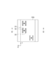
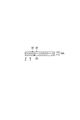
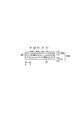
- FIG. 4 is a cross-sectional view of the laminated optical film taken along line IV-IV in FIG. 3.
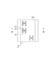
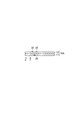
- FIG. 6 is a cross-sectional view of the laminated optical film taken along line VI-VI in FIG. 5. It is a figure for demonstrating the first marking process in the conventional defect inspection method, and is a figure which shows one main surface of the lamination
- FIG. 10 is a cross-sectional view of the laminated optical film along the line XX in FIG. 9. It is a figure which shows the defect inspection method and manufacturing method of a laminated optical film which concern on the 2nd Embodiment of this invention. It is a figure which shows the defect inspection method and manufacturing method of a laminated optical film which concern on the 2nd Embodiment of this invention. It is a figure for demonstrating the 1st marking process in the defect inspection method of the laminated optical film which concerns on the 2nd Embodiment of this invention, and is a figure which shows one main surface of a laminated optical film.
- FIG. 16 is a cross-sectional view of the laminated optical film taken along line XVI-XVI in FIG. 15.
- FIGS. 4 and 6 are views of the laminated optical film shown in FIG. 3 and FIG. It is sectional drawing. 1 to 6 show XY plane coordinates. The X direction indicates the width direction of the laminated optical film, and the Y direction indicates the longitudinal direction of the laminated optical film.
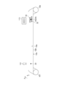
- the optical film 11 is unwound from the original fabric roll 101.
- the optical film 11 includes an optical film body having optical properties.
- the optical film 11 include a polarizing plate having polarization characteristics and a retardation plate having birefringence.
- the optical film body includes a polarizer (Polyvinyl Alcohol: PVA), and TAC (Triacetyl Cellulose) films are bonded to both sides of the main surface of the polarizer.
- PVA Polyvinyl Alcohol
- TAC Triacetyl Cellulose
- a light inspection device disposed on the one main surface 11a side of the optical film 11 by irradiating the optical film 11 with light by a light source (not shown) disposed on the other main surface 11b side of the optical film 11
- the light transmitted through the optical film 11 is received by 111, and a defect inspection of the optical film 11 is performed based on the received transmitted light (first inspection step, transmission inspection).
- the protective film 12 is unwound from the raw fabric roll 102, and the protective film 12 is laminated on the one main surface 11 a side of the optical film 11.
- a PET (Polyethylene Terephthalate) film or the like is used as the protective film 12.
- the optical film 11 and the protective film 12 are bonded together by the bonding roll 103 to generate a laminated optical film 10A.
- the protective film of the laminated optical film 10A corresponding to the defect detected in the first inspection step The surface on the 12th side is marked (first marking step).
- FIG. 4 schematically shows only one defect 20 in FIG. 3, and two linear marks 30 corresponding to the defect 20 are schematically shown.
- FIG. 1 schematically shows only one defect 20 in FIG. 3 and two linear marks 30 corresponding to the defect 20.
- the laminated optical film 10 ⁇ / b> A is wound around the original fabric roll 104.
- the laminated optical film 10 ⁇ / b> A is unwound from the original fabric roll 104, and the separate film (release film) 14 is bonded to the adhesive material 15 from the original fabric roll 105. 13 is fed out, and the adhesive film 13 with a separate film is laminated on the optical film 11 side of the laminated optical film 10A.
- PET Polyethylene Terephthalate
- the laminated optical film 10 ⁇ / b> A and the adhesive material 13 with a separate film are bonded together by the bonding roll 106 to generate a laminated optical film 10 ⁇ / b> B.
- the laminated optical film 10B is irradiated with light by a light source (not shown) arranged on the other main surface 10b side (separate film-attached adhesive material 13 side) of the laminated optical film 10B, and one side of the laminated optical film 10B.
- the light transmitted through the laminated optical film 10B is received by the inspector 115 arranged on the main surface 10a side (protective film 12 side) of the laminated optical film 10B, and defect inspection of the laminated optical film 10B is performed based on the received transmitted light (first). 2 inspection process, transmission inspection).
- the inspection device 115 is a transmission inspection device.
- the mark 30 marked in the first marking process is not detected.
- the mark 30 formed by a droplet method using an ink jet printer is usually large for a defect to be detected by inspection using a transmission inspection device.
- the inspector 115 can identify the mark 30 based on the size, for example.
- the inspector 115 may recognize the mark 30 based on the shape of the mark 30 marked in the first marking process.
- the inspector 115 may include a filter unit that excludes information related to the mark 30 from information included in the transmitted light received by the inspector 115.
- the laminated optical film 10B is subjected to the defect detected in the second inspection step. Marking is performed on the surface on the one main surface 10a side (second marking step).
- FIG. 6 schematically shows only one defect 20 in FIG. 3 and two linear marks 30 corresponding to the defect 20 as in FIG.
- FIG. 6 only one defect 21 in FIG. 5 is schematically shown, and two linear marks 31 corresponding to the defect 21 are schematically shown.
- 2 schematically shows only one defect 20 or 21 in FIG. 5 and two linear marks 30 or 31 corresponding to the defect 20 or 21 as in FIG.
- the laminated optical film 10 ⁇ / b> B is wound around the original fabric roll 107.
- FIGS. 7 and 9 are views showing one main surface of the laminated optical film in different steps of the conventional defect inspection method
- FIGS. 8 and 10 are cross-sectional views of the laminated optical film shown in FIGS. 7 and 9. It is.
- the conventional defect inspection method is different from the defect inspection method of the present embodiment in that the second inspection step does not have a function of not detecting the mark marked in the first marking step.
- the mark 30 formed in the first marking process is detected as a defect in the second inspection process.
- the second marking process corresponding to the defect 20 detected in the first inspection process and the mark 30 formed in the first marking process, these defects 20 and the mark 30 are sandwiched.
- a mark 31 is formed so as to surround the defect 20 and the mark 30.
- the defect inspection when the defect inspection is performed twice or more, in the second and subsequent inspections, the mark marked before the previous time is detected as a defect, and correspondingly, the defect is adjacent to the defect. Further, marking is performed, and as a result, the final mark size is increased, and the yield of the optical film is lowered.
- the defect inspection method and the manufacturing method of the laminated optical film of the first embodiment since the mark 30 marked in the first marking step is not detected in the second inspection step, two or more defect inspections are performed. When performing, it can prevent detecting the mark 30 corresponding to the defect detected before last time. As a result, the defect rate can be obtained with high accuracy, and the final mark size can be prevented from increasing, thereby preventing the yield of the optical film from being reduced.
- different inspections may be performed in combination on the same laminated optical film.
- the transmission inspection is suitable for detecting black foreign matters mixed inside the optical film, but it is difficult to detect small bubbles mixed on the optical film surface.
- the reflection inspection is suitable for detecting small bubbles mixed on the optical film surface, but it is difficult to detect black foreign matters mixed inside the optical film.
- a defect inspection method performed by combining different inspections on the same laminated optical film will be exemplified.
- a defect inspection method for a laminated optical film is exemplified, but the idea of the present invention can also be applied to a defect inspection method in which different inspections are performed on a single layer optical film.
- FIG. 11 and FIG. 12 are views showing a defect inspection method and a manufacturing method of a laminated optical film according to the second embodiment of the present invention.
- 13 and 15 are views showing one main surface of the laminated optical film in different steps of the defect inspection method shown in FIGS. 11 and 12, and
- FIGS. 14 and 16 are views showing the lamination shown in FIGS. It is sectional drawing of an optical film.
- the laminated optical film 10 ⁇ / b> B is fed out from the original fabric roll 101. And by the light source (not shown) arrange
- the laminated optical film 10A is subjected to the defect detected in the first inspection step. Marking is performed on the surface on the one main surface 10a side (first marking step).
- FIG. 14 only one defect 20 in FIG. 13 is schematically shown, and two linear marks 30 corresponding to the defect 20 are schematically shown.
- FIG. 11 schematically shows only one defect 20 in FIG. 13 and two linear marks 30 corresponding to the defect 20.
- the laminated optical film 10 ⁇ / b> B is wound around the original fabric roll 104.
- the laminated optical film 10 ⁇ / b> B is fed out from the original fabric roll 104.
- light was irradiated to the laminated optical film 10B by a light source (not shown) arranged on the one main surface 10a side of the laminated optical film 10B, and arranged on the one main surface 10a side of the laminated optical film 10B.
- the inspection device 115 receives the light reflected by the one main surface 10a of the laminated optical film 10B, and performs a defect inspection of the laminated optical film 10B based on the received reflected light (second inspection step, reflection inspection).
- the inspection device 115 is a reflection inspection device.
- the mark 30 marked in the first marking process is not detected. That is, in the second inspection process, the defect 25 which is not detected in the first inspection process and is detected for the first time in the second inspection process is detected (see FIGS. 15 and 16).
- the method for not detecting the mark 30 in the inspector 115 may be the same as that in the first embodiment. That is, the inspector 115 may recognize the mark 30 by its size, shape, and the like.
- the inspector 115 may include a filter unit that excludes information related to the mark 30 from information included in the received reflected light.
- the laminated optical film 10B is subjected to the defect detected in the second inspection step. Marking is performed on the surface on the one main surface 10a side (second marking step).
- FIG. 16 schematically shows only one defect 20 in FIG. 13 as well as two linear marks 30 corresponding to the defect 20, as in FIG. 14.
- FIG. 16 only one defect 25 in FIG. 15 is schematically shown, and two linear marks 31 corresponding to the defect 25 are schematically shown.
- FIG. 12 as in FIG. 11, only one defect 20 or 25 in FIG. 15 and two linear marks 30 or 31 corresponding to the defect 20 or 25 are schematically shown.
- the laminated optical film 10 ⁇ / b> B is wound up by the original fabric roll 107.
- the defect inspection method and manufacturing method of the laminated optical film of the second embodiment can also provide the same advantages as the defect inspection method and manufacturing method of the laminated optical film of the first embodiment.
- the present invention is not limited to the above-described embodiment, and various modifications can be made.
- the form in which the defect inspection is performed twice is illustrated, but the idea of the present invention can be applied to the form in which the defect inspection is performed three times or more.
- the transmission inspection and the reflection inspection are exemplified as the types of defect inspection, but the types of defect inspection are not limited thereto.
- the idea of the present invention can also be applied to a defect inspection method including a crossed Nicol inspection.
- 10A, 10B ... laminated optical film, 11 ... optical film, 12 ... protective film, 13 ... adhesive material with separate film, 14 ... separate film, 15 ... adhesive material, 20, 21, 25 ... defect, 30, 31 ... mark, 101, 102, 104, 105, 107 ... Raw fabric roll, 103, 106 ... Bonding roll, 111 ... Transmission inspection device, 113, 119 ... Inkjet printer, 115 ... Inspection device (transmission inspection device or reflection inspection device).
Landscapes
- Analytical Chemistry (AREA)
- Immunology (AREA)
- Physics & Mathematics (AREA)
- Health & Medical Sciences (AREA)
- Life Sciences & Earth Sciences (AREA)
- Chemical & Material Sciences (AREA)
- Pathology (AREA)
- General Health & Medical Sciences (AREA)
- Engineering & Computer Science (AREA)
- General Physics & Mathematics (AREA)
- Biochemistry (AREA)
- Textile Engineering (AREA)
- Computer Vision & Pattern Recognition (AREA)
- Signal Processing (AREA)
- Investigating Materials By The Use Of Optical Means Adapted For Particular Applications (AREA)
Abstract
Description
[第1の実施形態]
[第1の実施形態の変形例]
[第2の実施形態]
Claims (5)
- 光学フィルムに保護フィルム及び粘着材の少なくとも一方を貼り合せて積層光学フィルムを得ながら、前記積層光学フィルム中の欠陥を検査する方法であって、
前記光学フィルムの欠陥検査を行う第1検査工程と、
前記光学フィルムに前記保護フィルム及び前記粘着材の少なくとも一方を貼り合せて前記積層光学フィルムを生成する工程と、
前記第1検査工程において検出された欠陥に対応して前記積層光学フィルムにマーキングを行う第1マーキング工程と、
前記積層光学フィルムの欠陥検査を行う第2検査工程と、
前記第2検査工程において検出された欠陥に対応して前記積層光学フィルムにマーキングを行う第2マーキング工程と、
を含み、
前記第2検査工程では、前記第1マーキング工程においてマーキングされたマークを検出しない、
積層光学フィルムの欠陥検査方法。 - 前記第1検査工程における欠陥検査方法と前記第2検査工程における欠陥検査方法とは同一である、請求項1に記載の積層光学フィルムの欠陥検査方法。
- 前記第1検査工程における欠陥検査方法と前記第2検査工程における欠陥検査方法とは異なる、請求項1に記載の積層光学フィルムの欠陥検査方法。
- 光学フィルムの欠陥を検査する方法であって、
前記光学フィルムの欠陥検査を行う第1検査工程と、
前記第1検査工程において検出された欠陥に対応して前記光学フィルムにマーキングを行う第1マーキング工程と、
前記光学フィルムの欠陥検査であって、前記第1検査工程における欠陥検査とは異なる欠陥検査を行う第2検査工程と、
前記第2検査工程において検出された欠陥に対応して前記光学フィルムにマーキングを行う第2マーキング工程と、
を含み、
前記第2検査工程では、前記第1マーキング工程においてマーキングされたマークを検出しない、
光学フィルムの欠陥検査方法。 - 光学フィルムに保護フィルム及び粘着材の少なくとも一方を貼り合せて積層光学フィルムを製造する方法であって、
請求項1~3の何れか1項に記載の積層光学フィルムの欠陥検査方法を含む、
積層光学フィルムの製造方法。
Priority Applications (3)
| Application Number | Priority Date | Filing Date | Title |
|---|---|---|---|
| CN201680019040.8A CN107407642B (zh) | 2015-04-09 | 2016-03-28 | 层叠光学膜的缺陷检查方法以及层叠光学膜的制造方法 |
| JP2017511541A JP6749894B2 (ja) | 2015-04-09 | 2016-03-28 | 積層光学フィルムの欠陥検査方法、光学フィルムの欠陥検査方法及び積層光学フィルムの製造方法 |
| KR1020177027071A KR101898835B1 (ko) | 2015-04-09 | 2016-03-28 | 적층 광학 필름의 결함 검사 방법, 광학 필름의 결함 검사 방법 및 적층 광학 필름의 제조 방법 |
Applications Claiming Priority (2)
| Application Number | Priority Date | Filing Date | Title |
|---|---|---|---|
| JP2015080113 | 2015-04-09 | ||
| JP2015-080113 | 2015-04-09 |
Publications (1)
| Publication Number | Publication Date |
|---|---|
| WO2016163261A1 true WO2016163261A1 (ja) | 2016-10-13 |
Family
ID=57072618
Family Applications (1)
| Application Number | Title | Priority Date | Filing Date |
|---|---|---|---|
| PCT/JP2016/059934 Ceased WO2016163261A1 (ja) | 2015-04-09 | 2016-03-28 | 積層光学フィルムの欠陥検査方法、光学フィルムの欠陥検査方法及び積層光学フィルムの製造方法 |
Country Status (5)
| Country | Link |
|---|---|
| JP (1) | JP6749894B2 (ja) |
| KR (1) | KR101898835B1 (ja) |
| CN (1) | CN107407642B (ja) |
| TW (1) | TWI663391B (ja) |
| WO (1) | WO2016163261A1 (ja) |
Cited By (3)
| Publication number | Priority date | Publication date | Assignee | Title |
|---|---|---|---|---|
| CN108535259A (zh) * | 2017-03-03 | 2018-09-14 | 住友化学株式会社 | 缺陷标注方法及装置、卷料和片的制造方法及卷料和片 |
| CN112740083A (zh) * | 2018-07-30 | 2021-04-30 | 日本化药株式会社 | 标记装置、标记方法、偏振片制造方法以及偏振片 |
| WO2022149299A1 (ja) * | 2021-01-08 | 2022-07-14 | 日東電工株式会社 | 光学積層フィルムの検査方法及びフィルム製品の製造方法 |
Families Citing this family (3)
| Publication number | Priority date | Publication date | Assignee | Title |
|---|---|---|---|---|
| CN109212023A (zh) * | 2018-09-07 | 2019-01-15 | 深圳市哈德胜精密科技股份有限公司 | 一种石墨探伤方法 |
| WO2021117273A1 (ja) * | 2019-12-10 | 2021-06-17 | 日東電工株式会社 | 長尺光学積層体の検査方法及び検査システム |
| CN111452514B (zh) * | 2020-04-26 | 2021-01-12 | 杭州利珀科技有限公司 | 偏光膜整线打标系统及方法 |
Citations (4)
| Publication number | Priority date | Publication date | Assignee | Title |
|---|---|---|---|---|
| JPH06148097A (ja) * | 1992-11-13 | 1994-05-27 | Toshiba Corp | 欠陥検査装置 |
| WO2009123002A1 (ja) * | 2008-03-31 | 2009-10-08 | 住友化学株式会社 | 偏光フィルムの検査方法 |
| JP2013024868A (ja) * | 2011-07-25 | 2013-02-04 | Dongwoo Fine-Chem Co Ltd | フィルムの歩留まり予測システム及び方法 |
| JP2014130140A (ja) * | 2012-12-31 | 2014-07-10 | Dongwoo Fine-Chem Co Ltd | 測定結果検証システム |
Family Cites Families (11)
| Publication number | Priority date | Publication date | Assignee | Title |
|---|---|---|---|---|
| JP4343456B2 (ja) * | 2001-04-03 | 2009-10-14 | 大日本印刷株式会社 | シート状製品の欠陥マーキング方法および装置 |
| JP2006194721A (ja) * | 2005-01-13 | 2006-07-27 | Nagase & Co Ltd | 欠陥マーキング装置 |
| TWI366706B (en) * | 2006-07-03 | 2012-06-21 | Olympus Corp | Semiconductor substrate defects detection device and method of detection of defects |
| JP2009069142A (ja) | 2007-08-23 | 2009-04-02 | Nitto Denko Corp | 積層フィルムの欠陥検査方法およびその装置 |
| EP2295930B1 (en) * | 2008-06-04 | 2014-01-01 | Kabushiki Kaisha Kobe Seiko Sho | Tire shape inspection method and tire shape inspection device |
| JP4776739B2 (ja) | 2009-04-10 | 2011-09-21 | 日東電工株式会社 | 光学フィルムロール原反を用いた画像表示装置の製造方法 |
| KR101311497B1 (ko) * | 2011-10-20 | 2013-10-14 | 주식회사 엘지화학 | 광학 필름의 결함 검사 장치 |
| JP5944175B2 (ja) * | 2012-02-07 | 2016-07-05 | 住友ゴム工業株式会社 | タイヤ用部材の製造装置および製造方法 |
| JP6182806B2 (ja) | 2013-06-04 | 2017-08-23 | 住友化学株式会社 | 欠陥検査システム及びフィルムの製造装置 |
| JP2015049350A (ja) | 2013-08-30 | 2015-03-16 | 住友化学株式会社 | 光学部材貼合体の製造方法 |
| JP6641093B2 (ja) * | 2015-03-20 | 2020-02-05 | 住友化学株式会社 | 光学フィルム及び積層光学フィルムの欠陥検査方法 |
-
2016
- 2016-03-28 JP JP2017511541A patent/JP6749894B2/ja active Active
- 2016-03-28 KR KR1020177027071A patent/KR101898835B1/ko active Active
- 2016-03-28 WO PCT/JP2016/059934 patent/WO2016163261A1/ja not_active Ceased
- 2016-03-28 CN CN201680019040.8A patent/CN107407642B/zh active Active
- 2016-03-31 TW TW105110395A patent/TWI663391B/zh active
Patent Citations (4)
| Publication number | Priority date | Publication date | Assignee | Title |
|---|---|---|---|---|
| JPH06148097A (ja) * | 1992-11-13 | 1994-05-27 | Toshiba Corp | 欠陥検査装置 |
| WO2009123002A1 (ja) * | 2008-03-31 | 2009-10-08 | 住友化学株式会社 | 偏光フィルムの検査方法 |
| JP2013024868A (ja) * | 2011-07-25 | 2013-02-04 | Dongwoo Fine-Chem Co Ltd | フィルムの歩留まり予測システム及び方法 |
| JP2014130140A (ja) * | 2012-12-31 | 2014-07-10 | Dongwoo Fine-Chem Co Ltd | 測定結果検証システム |
Cited By (7)
| Publication number | Priority date | Publication date | Assignee | Title |
|---|---|---|---|---|
| CN108535259A (zh) * | 2017-03-03 | 2018-09-14 | 住友化学株式会社 | 缺陷标注方法及装置、卷料和片的制造方法及卷料和片 |
| JP2018146580A (ja) * | 2017-03-03 | 2018-09-20 | 住友化学株式会社 | 欠陥マーキング方法及び欠陥マーキング装置、原反の製造方法及び原反、並びにシートの製造方法及びシート |
| CN112740083A (zh) * | 2018-07-30 | 2021-04-30 | 日本化药株式会社 | 标记装置、标记方法、偏振片制造方法以及偏振片 |
| CN112740083B (zh) * | 2018-07-30 | 2023-03-14 | 日本化药株式会社 | 标记装置、标记方法、偏振片制造方法以及偏振片 |
| WO2022149299A1 (ja) * | 2021-01-08 | 2022-07-14 | 日東電工株式会社 | 光学積層フィルムの検査方法及びフィルム製品の製造方法 |
| JP2022107419A (ja) * | 2021-01-08 | 2022-07-21 | 日東電工株式会社 | 光学積層フィルムの検査方法及びフィルム製品の製造方法 |
| JP7594917B2 (ja) | 2021-01-08 | 2024-12-05 | 日東電工株式会社 | 光学積層フィルムの検査方法及びフィルム製品の製造方法 |
Also Published As
| Publication number | Publication date |
|---|---|
| TWI663391B (zh) | 2019-06-21 |
| TW201640100A (zh) | 2016-11-16 |
| CN107407642A (zh) | 2017-11-28 |
| JPWO2016163261A1 (ja) | 2018-02-08 |
| CN107407642B (zh) | 2020-04-03 |
| KR20170118933A (ko) | 2017-10-25 |
| JP6749894B2 (ja) | 2020-09-02 |
| KR101898835B1 (ko) | 2018-09-13 |
Similar Documents
| Publication | Publication Date | Title |
|---|---|---|
| JP6749894B2 (ja) | 積層光学フィルムの欠陥検査方法、光学フィルムの欠陥検査方法及び積層光学フィルムの製造方法 | |
| JP6641093B2 (ja) | 光学フィルム及び積層光学フィルムの欠陥検査方法 | |
| JP6177017B2 (ja) | 欠陥検査システム | |
| TWI766952B (zh) | 缺陷標記方法及缺陷標記裝置、原材的製造方法及原材,以及片的製造方法及片 | |
| JPWO2009128241A1 (ja) | 連続ウェブ形態の切込線入り光学フィルム積層体の連続ロール並びにその製造方法及び製造装置 | |
| JP2019053057A (ja) | 欠陥検査装置、欠陥検査方法、円偏光板又は楕円偏光板の製造方法及び位相差板の製造方法 | |
| CN101981438A (zh) | 偏光薄膜的检查方法 | |
| WO2015182541A1 (ja) | 積層偏光フィルムの欠陥検査方法、製造方法および製造装置 | |
| US9902143B2 (en) | Method and device for forming laminated substrate | |
| JP6437329B2 (ja) | 光学フィルムの欠陥検査方法 | |
| JP2017068121A (ja) | 偏光子の検査方法および偏光板の製造方法 | |
| JP2019215371A (ja) | 光学フィルム及び積層光学フィルムの欠陥検査方法 | |
| JP2018146360A (ja) | 欠陥情報読取方法、欠陥情報読取装置及び欠陥情報読取システム | |
| TW202129264A (zh) | 長條光學積層體之檢查方法及檢查系統 | |
| JP4160418B2 (ja) | フィルム層間剥離防止方法 | |
| TWI762592B (zh) | 缺陷檢查系統、膜製造裝置、膜製造方法、印字裝置及印字方法 | |
| CN114654096A (zh) | 带有标记的光学层叠体、以及带有标记的光学层叠体的制造方法 | |
| CN106471402A (zh) | 光学构件、光学显示设备的生产系统、光学显示设备的生产方法及卷料卷筒 | |
| JP2022044597A (ja) | 光学フィルム原反ロールの製造方法、および光学部材シートの製造方法 |
Legal Events
| Date | Code | Title | Description |
|---|---|---|---|
| 121 | Ep: the epo has been informed by wipo that ep was designated in this application |
Ref document number: 16776429 Country of ref document: EP Kind code of ref document: A1 |
|
| ENP | Entry into the national phase |
Ref document number: 2017511541 Country of ref document: JP Kind code of ref document: A |
|
| ENP | Entry into the national phase |
Ref document number: 20177027071 Country of ref document: KR Kind code of ref document: A |
|
| NENP | Non-entry into the national phase |
Ref country code: DE |
|
| 122 | Ep: pct application non-entry in european phase |
Ref document number: 16776429 Country of ref document: EP Kind code of ref document: A1 |