WO2016158601A1 - Ledモジュールおよびledモジュールの製造方法 - Google Patents
Ledモジュールおよびledモジュールの製造方法 Download PDFInfo
- Publication number
- WO2016158601A1 WO2016158601A1 PCT/JP2016/059128 JP2016059128W WO2016158601A1 WO 2016158601 A1 WO2016158601 A1 WO 2016158601A1 JP 2016059128 W JP2016059128 W JP 2016059128W WO 2016158601 A1 WO2016158601 A1 WO 2016158601A1
- Authority
- WO
- WIPO (PCT)
- Prior art keywords
- thin film
- sealing resin
- led module
- led chip
- light
- Prior art date
- Legal status (The legal status is an assumption and is not a legal conclusion. Google has not performed a legal analysis and makes no representation as to the accuracy of the status listed.)
- Ceased
Links
Images


Classifications
-
- H—ELECTRICITY
- H10—SEMICONDUCTOR DEVICES; ELECTRIC SOLID-STATE DEVICES NOT OTHERWISE PROVIDED FOR
- H10H—INORGANIC LIGHT-EMITTING SEMICONDUCTOR DEVICES HAVING POTENTIAL BARRIERS
- H10H20/00—Individual inorganic light-emitting semiconductor devices having potential barriers, e.g. light-emitting diodes [LED]
- H10H20/80—Constructional details
- H10H20/85—Packages
- H10H20/855—Optical field-shaping means, e.g. lenses
- H10H20/856—Reflecting means
-
- H—ELECTRICITY
- H10—SEMICONDUCTOR DEVICES; ELECTRIC SOLID-STATE DEVICES NOT OTHERWISE PROVIDED FOR
- H10H—INORGANIC LIGHT-EMITTING SEMICONDUCTOR DEVICES HAVING POTENTIAL BARRIERS
- H10H20/00—Individual inorganic light-emitting semiconductor devices having potential barriers, e.g. light-emitting diodes [LED]
- H10H20/80—Constructional details
- H10H20/85—Packages
- H10H20/852—Encapsulations
-
- H—ELECTRICITY
- H10—SEMICONDUCTOR DEVICES; ELECTRIC SOLID-STATE DEVICES NOT OTHERWISE PROVIDED FOR
- H10H—INORGANIC LIGHT-EMITTING SEMICONDUCTOR DEVICES HAVING POTENTIAL BARRIERS
- H10H20/00—Individual inorganic light-emitting semiconductor devices having potential barriers, e.g. light-emitting diodes [LED]
- H10H20/80—Constructional details
- H10H20/85—Packages
- H10H20/852—Encapsulations
- H10H20/853—Encapsulations characterised by their shape
-
- H—ELECTRICITY
- H10—SEMICONDUCTOR DEVICES; ELECTRIC SOLID-STATE DEVICES NOT OTHERWISE PROVIDED FOR
- H10H—INORGANIC LIGHT-EMITTING SEMICONDUCTOR DEVICES HAVING POTENTIAL BARRIERS
- H10H20/00—Individual inorganic light-emitting semiconductor devices having potential barriers, e.g. light-emitting diodes [LED]
- H10H20/80—Constructional details
- H10H20/85—Packages
- H10H20/857—Interconnections, e.g. lead-frames, bond wires or solder balls
-
- H—ELECTRICITY
- H10—SEMICONDUCTOR DEVICES; ELECTRIC SOLID-STATE DEVICES NOT OTHERWISE PROVIDED FOR
- H10H—INORGANIC LIGHT-EMITTING SEMICONDUCTOR DEVICES HAVING POTENTIAL BARRIERS
- H10H20/00—Individual inorganic light-emitting semiconductor devices having potential barriers, e.g. light-emitting diodes [LED]
- H10H20/80—Constructional details
- H10H20/84—Coatings, e.g. passivation layers or antireflective coatings
-
- H—ELECTRICITY
- H10—SEMICONDUCTOR DEVICES; ELECTRIC SOLID-STATE DEVICES NOT OTHERWISE PROVIDED FOR
- H10H—INORGANIC LIGHT-EMITTING SEMICONDUCTOR DEVICES HAVING POTENTIAL BARRIERS
- H10H20/00—Individual inorganic light-emitting semiconductor devices having potential barriers, e.g. light-emitting diodes [LED]
- H10H20/80—Constructional details
- H10H20/85—Packages
- H10H20/855—Optical field-shaping means, e.g. lenses
-
- H—ELECTRICITY
- H10—SEMICONDUCTOR DEVICES; ELECTRIC SOLID-STATE DEVICES NOT OTHERWISE PROVIDED FOR
- H10W—GENERIC PACKAGES, INTERCONNECTIONS, CONNECTORS OR OTHER CONSTRUCTIONAL DETAILS OF DEVICES COVERED BY CLASS H10
- H10W72/00—Interconnections or connectors in packages
- H10W72/071—Connecting or disconnecting
- H10W72/075—Connecting or disconnecting of bond wires
- H10W72/07551—Connecting or disconnecting of bond wires characterised by changes in properties of the bond wires during the connecting
- H10W72/07554—Connecting or disconnecting of bond wires characterised by changes in properties of the bond wires during the connecting changes in dispositions
-
- H—ELECTRICITY
- H10—SEMICONDUCTOR DEVICES; ELECTRIC SOLID-STATE DEVICES NOT OTHERWISE PROVIDED FOR
- H10W—GENERIC PACKAGES, INTERCONNECTIONS, CONNECTORS OR OTHER CONSTRUCTIONAL DETAILS OF DEVICES COVERED BY CLASS H10
- H10W72/00—Interconnections or connectors in packages
- H10W72/50—Bond wires
- H10W72/541—Dispositions of bond wires
- H10W72/547—Dispositions of multiple bond wires
Definitions
- the present invention relates to an LED module with improved light extraction efficiency and a method for manufacturing the same.
- LED modules in which LED chips are sealed with resin have been widely used as lighting fixtures.
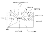
- the general structure of the LED module is that the LED chip 2 is mounted on the electrode 5 of the package substrate 1 as shown in the cross-sectional view of FIG.
- the reflector 4 that reflects light around the LED chip 2 is disposed, and the sealing resin 3 is applied to the inner peripheral surface of the reflector 4, the wire 6, the LED chip 2, and the electrode 5 of the package substrate. It has a filled structure.
- the light emitted from the LED chip 2 is reflected by the reflector 4 or travels straight through the sealing resin 3 and is emitted from the substantially flat surface of the sealing resin 3 to the atmosphere.
- the reflector 4 or travels straight through the sealing resin 3 and is emitted from the substantially flat surface of the sealing resin 3 to the atmosphere.
- Japanese Patent Application Laid-Open No. 2009-147329 discloses a textured surface of a sealing resin in order to reduce internal reflection of light at a sealing body of an LED module and reduce loss in light output to the atmosphere. What is processed is described.
- Patent Document 1 does not specifically show the textured processing method or the form of the material at the interface with the atmosphere, and is unknown.
- An object of the present invention is to embody a form for solving the problem of an output loss of light emitted to the atmosphere in an LED module.
- the present invention provides an LED module in which an LED chip is sealed with a sealing resin, the surface of the sealing resin being covered with a thin film, and the thin film is the sealing resin
- the present invention provides an LED module comprising a material having a smaller linear expansion coefficient than that of the thin film, and having an uneven surface on the surface of the thin film so that light from the LED chip is multiply reflected. .
- the angle at which the light emitted from the LED chip is internally reflected on the surface of the sealing resin is diversified and complicated (ie, multiple reflections are performed), and the probability of light emitted to the atmosphere. This improves the light extraction efficiency by reducing the output loss of light to the atmosphere.
- the thin film may have a structure in which irregularities are formed on the surface of the thin film by forming the thin film on the surface of the sealing resin under heating conditions and then returning to room temperature.
- the thin film may include an oxide film made of an inorganic material.
- the thin film may have a structure in which a buffer film made of an inorganic material is laminated between the oxide film and the sealing resin.
- the present invention provides a sealing step of sealing an LED chip mounted on a package substrate with a sealing resin, and the sealing resin under heating conditions after the sealing step.
- the present invention provides a method for manufacturing an LED module, characterized by being reflected.
- the angle at which the light emitted from the LED chip is reflected at the interface with the atmosphere is diversified and complicated (ie, multiple reflection), and the output loss of the light emitted to the atmosphere is reduced.
- the light extraction efficiency can be improved.
- an LED module in which an LED chip is sealed with a sealing resin, the surface of the sealing resin is covered with a thin film, and the thin film has a smaller linear expansion coefficient than the sealing resin.
- the LED module is made of a material, and the surface of the thin film is provided with an uneven surface so that the light from the LED chip is reflected multiple times. Thus, the light is efficiently reflected, and the output loss of the light emitted to the atmosphere can be reduced to improve the light extraction efficiency.
- the LED module is characterized in that after the film forming step, the LED module is returned to room temperature to form irregularities on the surface of the thin film so that light from the LED chip is multiply reflected.
- FIG. 1 shows a cross section of the LED module.
- the LED chip 2 is mounted on the electrode 5 of the package substrate 1, and the electrode of the LED chip 2 and the electrode 5 of the package substrate are electrically connected by a wire 6.
- a reflector 4 made of ceramic or the like is disposed around the LED chip 2 so that a part of the light emitted from the LED chip 2 is reflected and travels to the atmosphere, so that more light is emitted from the LED module. It is supposed to be.
- Example 1 the electrode of the LED chip 2 and the electrode 5 of the package substrate 1 are connected by the wire 6.
- the present invention is not necessarily limited to this, and the LED chip 2 is connected to the electrode of the package substrate 1. 5 may be flip-chip bonded and electrically connected without using the wire 6.
- the space surrounded by the reflector 4, the LED chip 2, and the package substrate 1 is filled with a sealing resin 3 made of silicone resin and sealed from the atmosphere.
- the boundary between the sealing resin 3 and the atmosphere is covered with a thin film 7 and has an uneven surface.
- the thin film 7 is configured as an oxide film made of an inorganic material.
- the thin film 7 is made of a material having a linear expansion coefficient smaller than that of the sealing resin 3. More specifically, the linear expansion coefficient of the thin film 7 is preferably 1 to 10 ppm / ° C., and the linear expansion coefficient of the sealing resin 3 is preferably 100 to 500 ppm / ° C.
- the thickness of the thin film 7 may be about 1 ⁇ m, but it may be greater than or less than this.
- the refractive index of the thin film 7 is preferably the same as that of the sealing resin 3 or a material having a value between the atmosphere and the sealing resin 3.
- the thin film 7 is formed using SiO 2 in the first embodiment, the thin film 7 is not necessarily limited to this, and may be an oxide film made of another inorganic material whose linear expansion coefficient is smaller than that of the sealing resin 3. For example, you may form using Al2O3.
- the thin film 7 By forming the thin film 7 with a material having a smaller linear expansion coefficient than that of the sealing resin 3 under heating, the expanded sealing resin 3 is pulled by the contraction when returning to room temperature, so that the thin film 7 can be wrinkled. Irregularities having a height of about 1 to 200 ⁇ m can be formed on the surface of the thin film 7 relatively easily.
- an inorganic substance is a substance excluding an organic substance, specifically, a substance having no carbon skeleton, and has a small linear expansion coefficient. That is, the inorganic substance does not include synthetic / natural resins and other compounds having a carbon skeleton (including a hydrocarbon skeleton).
- an oxide film made of an inorganic substance has a strong bonding force and a high barrier property.
- the bonding force is high, cracks are difficult to occur. That is, by forming the thin film 7 having irregularities on the surface as an oxide film made of an inorganic substance, it is possible to reduce the output loss of light emitted to the atmosphere and improve the light extraction efficiency, It is possible to prevent air from entering the sealing resin and corroding the electrode.
- the light emitted from the LED chip 2 passes through the sealing resin 3 or is reflected by the reflector and reaches the uneven surface of the thin film 7.
- the light is reflected repeatedly in various directions on the uneven surface of the thin film 7 (that is, multiple reflections), so that the internal reflection B is suppressed and more light A is emitted to the atmosphere. Can be improved.
- the manufacturing method of the LED module of this invention is demonstrated.
- the LED chip 2 is mounted on the electrode 5 of the package substrate 1 having the reflector 4, and the LED chip electrode and the substrate electrode are electrically connected by a wire 6 and sealed in a module space.
- a thin film 7 is formed on the surface of the sealing resin 3 by a plasma CVD apparatus on the LED module filled with the resin 3.
- the sealing resin 3 expands by heating the LED module.
- the sealing resin 3 having a large linear expansion coefficient contracts, so that the inorganic oxide film made of SiO2 is also pulled and contracts.
- SiO2 has a linear expansion coefficient smaller than that of the sealing resin 3, fine irregularities are formed when the lost SiO2 is wrinkled.
- FIG. 2 shows a state in which SiO2 is wrinkled and unevenness is formed.
- an uneven surface (wrinkle) as shown in FIG. 2 can be formed when the film is heated to 40 ° C. to 130 ° C. and then returned to room temperature.
- the plasma CVD is used to form the thin film 7 which is an inorganic oxide film made of SiO 2
- the present invention is not necessarily limited thereto, and the film is formed under heating, such as a sputtering apparatus or a vapor deposition apparatus. Anything can be used.
- the inorganic oxide film is not limited to SiO2, and the same manufacturing method is used to form irregularities (wrinkles) on the surface of the thin film 7 even with Al2O3 having a smaller linear expansion coefficient than the sealing resin 3 made of silicone resin. Can do.
- the LED module in Example 2 of the present invention is different from Example 1 in that the thin film 7 has a laminated structure. That is, a buffer layer, which is an insulating film made of an inorganic material, is formed on the surface of the sealing resin 3, and an oxide film made of an inorganic material is further formed on the surface. That is, a buffer layer, which is an insulating film made of an inorganic material, is laminated between the oxide film made of an inorganic material and the sealing resin 3.
- the buffer layer is a film having a lower barrier property than the oxide film but having a higher adhesion than the oxide film, and is an inorganic substance made of a material having a smaller linear expansion coefficient than the sealing resin 3.
- the buffer layer may be a silicon-based film containing H, C, and Si. More specifically, a SiCN film may be used, but the present invention is not necessarily limited thereto, and a SiN film or a SiON film may be used.
- Adhesion with the sealing resin 3 can be improved by laminating a buffer layer made of an inorganic material between the sealing resin 3 and an oxide film made of an inorganic material.
- the heating temperature during film formation that can form irregularities on the thin film 7 without generating cracks can be made higher than 130 ° C.
- Example 2 the light emitted from the LED chip 2 passes through the sealing resin 3 or is reflected by the reflector and reaches the uneven surface of the thin film 7.
- the light is reflected repeatedly in various directions on the uneven surface of the thin film 7 (that is, multiple reflections), so that the internal reflection B is suppressed and more light A is emitted to the atmosphere. Can be improved.
- the oxide film made of an inorganic substance in the thin film 7 is formed using SiO2.
- the present invention is not necessarily limited thereto, and may be an oxide film made of another inorganic material having a linear expansion coefficient smaller than that of the sealing resin 3. For example, you may form using Al2O3.
- Example 2 the buffer layer and the oxide film are stacked one by one.
- the present invention is not limited to this, and a plurality of layers may be stacked alternately. Thereby, barrier property can be made high, maintaining adhesiveness.
- the LED chip 2 is mounted on the electrode 5 of the package substrate 1 having the reflector 4, and the sealing resin 3 fills the space of the module in which the LED chip electrode and the substrate electrode 5 are electrically connected by the wire 6.
- a buffer layer which is an insulating layer made of an inorganic material, is formed on the surface of the sealing resin 3 on the surface of the sealing module 3 using a plasma CVD apparatus.
- the buffer layer can be SiCN.
- an inorganic oxide film made of SiO 2 is formed on the surface of the buffer layer in the same plasma CVD apparatus, and the thin film 7 is constituted by the buffer layer made of SiCN and the oxide film made of SiO 2.
- the sealing resin 3 made of silicone resin having a large linear expansion coefficient contracts, so that it is made of an inorganic oxide film made of SiO2 and SiCN.
- the buffer layer is also pulled and contracted by this, SiO2 and SiCN have a linear expansion coefficient smaller than that of the sealing resin 3 made of silicone resin, so that unevenness is formed when the lost SiO2 and SiCN wrinkle.
- the light emitted from the LED chip 2 passes through the sealing resin 3 or is reflected by the reflector and reaches the uneven surface of the thin film 7.
- the light is reflected repeatedly in various directions on the uneven surface of the thin film 7 (that is, multiple reflections), so that the internal reflection B is suppressed and more light A is emitted to the atmosphere. Can be improved.
- Example 2 the electrode of the LED chip 2 and the electrode 5 of the package substrate 1 are connected by the wire 6, but the present invention is not necessarily limited to this, and the LED chip 2 is connected to the electrode of the package substrate 1. 5 may be flip-chip bonded and electrically connected without using the wire 6.
- the apparatus used for forming the thin film 7 is not limited to plasma CVD, and any apparatus capable of forming a film under heating, such as a sputtering apparatus or a vapor deposition apparatus, can be used.
- the inorganic oxide film is not limited to SiO 2, and unevenness (wrinkles) can be formed on the surface of the thin film 7 by Al 2 O 3 by the same manufacturing method.
- the present invention can be widely applied to LED modules and LED module manufacturing methods.
Landscapes
- Led Device Packages (AREA)
Abstract
LEDモジュールにおいて、大気に放出される光の出力ロスが生じるという問題を解決するための形態を具体化する。具体的には、LEDチップが封止樹脂で封止されたLEDモジュールであって、当該封止樹脂の表面が薄膜で覆われており、前記薄膜は前記封止樹脂よりも線膨張係数が小さい材質からなり、前記薄膜の表面には凹凸面を備えることによって前記LEDチップからの光が多重反射するように構成した。
Description
本発明は、光の取り出し効率を向上させたLEDモジュールおよびその製造方法に関するものである。
従来から、LEDチップを樹脂で封止したLEDモジュールが照明具として広く用いられている。LEDモジュールの一般的な構造は、図3に示す断面図のようにパッケージ基板1の電極5上にLEDチップ2を搭載し、そのLEDチップ2の電極とパッケージ基板1の電極5とをワイヤー6で電気的に接続するととともに、LEDチップ2の周囲に光を反射させるリフレクター4を配置し、リフレクター4の内周面、ワイヤー6、及びLEDチップ2並びにパッケージ基板の電極5に封止樹脂3を充填した構造となっている。
LEDチップ2で発光した光は、リフレクター4で反射する光や直進する光が封止樹脂3を通過し、ほぼ平坦な封止樹脂3表面から大気に放出される。そのときに図3に示すように大気と封止樹脂3の屈折率差から封止樹脂3表面で内部反射Bする光が多く、大気に放出される光Aの出力にロスが生じるという問題があった。
特開2009-147329号公報には、LEDモジュールの封止体での光の内部反射を低減して、大気に放出される光の出力にロスを低減するために封止樹脂の表面にテクスチャード加工するものが記載されている。
しかしながら、特許文献1には、具体的なテクスチャード加工の方法や大気との界面における材質といった形態が、具体的に示されておらず不明である。
本発明は、LEDモジュールにおいて大気に放出される光の出力ロスが生じるという問題を解決するための形態を具体化することを課題とする。
上記の課題を解決するために本発明は、LEDチップが封止樹脂で封止されたLEDモジュールであって、当該封止樹脂の表面が薄膜で覆われており、前記薄膜は前記封止樹脂よりも線膨張係数が小さい材質からなり、前記薄膜の表面には凹凸面を備えることによって前記LEDチップからの光が多重反射するように構成したことを特徴とするLEDモジュールを提供するものである。
この構成により、LEDチップが発光した光が封止樹脂表面にて内部反射する角度が多様化・複雑化するようになり(すなわち、多重反射するようになり)、大気に放出される光の確率が向上し、大気への光の出力ロスを低減して光の取り出し効率を向上させることができる。
また、前記薄膜は、加熱条件下で前記封止樹脂表面に成膜した後、室温に戻すことにより前記薄膜の表面に凹凸が形成された構成としてもよい。
この構成により、線膨張係数の大きい前記封止樹脂が加熱によって膨張した状態で前記封止樹脂表面に薄膜を成膜することにより、室温に戻る際に前記封止樹脂が収縮することにより前記薄膜が引っ張られることによって、比較的簡単に前記薄膜表面に微細な凹凸が形成できる。
また、前記薄膜は、無機物からなる酸化膜を含む構成にしてもよい。
この構成により、大気に放出される光の出力ロスを低減して光の取り出し効率を向上させることができるとともに、水分や空気が封止樹脂内に入り込んで電極が腐食することを防止することができる。
また、前記薄膜は、前記酸化膜と前記封止樹脂との間に無機物からなるバッファ膜を積層する構成としてもよい。
この構成により、前記酸化膜と前記封止樹脂との密着性が向上し、成膜時の温度を高温にしてもクラックが生じることなく、より多くの凹凸を形成することができる。
また、上記の課題を解決するために本発明は、パッケージ基板に搭載されたLEDチップを封止樹脂で封止する封止工程と、該封止工程の後に、加熱条件下で前記封止樹脂の表面に薄膜を成膜する成膜工程とを有し、該成膜工程の後に前記LEDモジュールを室温に戻すことにより前記薄膜の表面に凹凸を形成して、前記LEDチップからの光が多重反射するようにしたことを特徴とするLEDモジュールの製造方法を提供するものである。
この製造方法により製造したLEDモジュールは、LEDチップが発光した光が大気との界面において反射する角度が多様化・複雑化(すなわち、多重反射)して、大気に放出される光の出力ロスを低減して光の取り出し効率を向上させることができる。
上記のように、LEDチップが封止樹脂で封止されたLEDモジュールであって、当該封止樹脂の表面が薄膜で覆われており、前記薄膜は前記封止樹脂よりも線膨張係数が小さい材質からなり、前記薄膜の表面には凹凸面を備えることによって前記LEDチップからの光が多重反射するように構成したことを特徴とするLEDモジュールにより、LEDチップが発光した光が封止樹脂表面にて多重反射するようになり、大気に放出される光の出力ロスを低減して光の取り出し効率を向上させることができる。
また、パッケージ基板に搭載されたLEDチップを封止樹脂で封止する封止工程と、該封止工程の後に、加熱条件下で前記封止樹脂の表面に薄膜を成膜する成膜工程とを有し、該成膜工程の後に前記LEDモジュールを室温に戻すことにより前記薄膜の表面に凹凸を形成して、前記LEDチップからの光が多重反射するようにしたことを特徴とするLEDモジュールの製造方法により、LEDチップが発光した光が封止樹脂表面にて多重反射するようになり、大気に放出される光の出力ロスを低減して光の取り出し効率を向上させることができる。
(LEDモジュール)
図1を用いて、本発明の実施例1におけるLEDモジュールの構成を説明する。図1はLEDモジュールの断面を示している。パッケージ基板1の電極5上にLEDチップ2が搭載され、そのLEDチップ2の電極とパッケージ基板の電極5とがワイヤー6で電気的に接続されている。また、LEDチップ2の周囲には、セラミック等からなるリフレクター4が配置されてLEDチップ2が発光した光の一部が反射して大気に向かうことにより、より多くの光がLEDモジュールから放出されるようにされている。
図1を用いて、本発明の実施例1におけるLEDモジュールの構成を説明する。図1はLEDモジュールの断面を示している。パッケージ基板1の電極5上にLEDチップ2が搭載され、そのLEDチップ2の電極とパッケージ基板の電極5とがワイヤー6で電気的に接続されている。また、LEDチップ2の周囲には、セラミック等からなるリフレクター4が配置されてLEDチップ2が発光した光の一部が反射して大気に向かうことにより、より多くの光がLEDモジュールから放出されるようにされている。
なお、実施例1においては、LEDチップ2の電極とパッケージ基板1の電極5とをワイヤー6で接続しているが、必ずしもこれに限定されるものではなく、LEDチップ2をパッケージ基板1の電極5にフリップチップボンディングして、ワイヤー6を用いることなく電気的に接続したものでもよい。
リフレクター4、LEDチップ2、パッケージ基板1に囲まれた空間には、シリコーン樹脂からなる封止樹脂3が充填されて大気から封止されている。また、封止樹脂3と大気との境界は薄膜7で覆われており、凹凸面を備えている。
薄膜7は、無機物からなる酸化膜として構成されている。また薄膜7は、線膨張係数が封止樹脂3より小さい材質からなっている。より具体的には、薄膜7の線膨張係数は1~10ppm/℃、封止樹脂3の線膨張係数は100~500ppm/℃であることが好ましい。
薄膜7の厚さは、1μm程度であってよいが、これ以上の厚さであってもこれ以下の厚さであってもよい。
また、薄膜7の屈折率は封止樹脂3と同等、又は大気と封止樹脂3の間の値をもつ材質が好ましい。
薄膜7は、実施例1においてはSiO2を用いて形成しているが、必ずしもこれに限定されるものではなく、線膨張係数が封止樹脂3より小さい他の無機物からなる酸化膜でよい。例えば、Al2O3を用いて形成してもよい。
封止樹脂3より線膨張係数が小さい材質で薄膜7を加熱下で成膜することにより、膨張していた封止樹脂3が室温に戻る際の収縮に引っ張られて薄膜7にしわができるため、比較的簡単に薄膜7の表面に高さが1~200μm程度の凹凸を形成することができる。
なお、無機物とは、有機物を除く物質であり、具体的には炭素骨格を持たない物質であり、線膨張係数が小さい。つまり無機物には、合成/天然樹脂及び炭素骨格(炭化水素骨格を含む)を有するその他化合物は含まれない。
特に、無機物からなる酸化膜は結合力が強く、バリア性が高い。また、結合力が高いためクラックが入りにくい。つまり、無機物からなる酸化膜として表面に凹凸を有する薄膜7を成膜することにより、大気に放出される光の出力ロスを低減して、光の取り出し効率を向上させることができるとともに、水分や空気が封止樹脂内に入り込んで電極が腐食することを防止することができる。
LEDチップ2から発光した光は封止樹脂3内を通過して、又はリフレクターで反射して、薄膜7の凹凸面に達する。薄膜7の凹凸面で光は多様な方向に複雑に反射を繰り返す(すなわち多重反射する)ことにより、内部反射Bが抑制されてより大気に放射される光Aが多くなるので、光の取り出し効率を向上させることができる。
(製造方法)
次に、本発明のLEDモジュールの製造方法について説明する。図1のようにリフレクター4を備えたパッケージ基板1の電極5上にLEDチップ2が搭載され、LEDチップの電極と基板の電極とがワイヤー6で電気的に接続されたモジュールの空間に封止樹脂3が充填されたLEDモジュールに対して、プラズマCVD装置により封止樹脂3の表面に薄膜7を成膜する。
次に、本発明のLEDモジュールの製造方法について説明する。図1のようにリフレクター4を備えたパッケージ基板1の電極5上にLEDチップ2が搭載され、LEDチップの電極と基板の電極とがワイヤー6で電気的に接続されたモジュールの空間に封止樹脂3が充填されたLEDモジュールに対して、プラズマCVD装置により封止樹脂3の表面に薄膜7を成膜する。
その際、LEDモジュールが加熱されることにより封止樹脂3が膨張する。その膨張した封止樹脂3の表面に線膨張係数が封止樹脂3より小さい材質であるSiO2からなる無機物の酸化膜を成膜して薄膜7とする。そしてプラズマCVD装置からLEDモジュールを取り出して室温に戻す際に、線膨張係数の大きい封止樹脂3が収縮することにより、成膜されているSiO2からなる無機物の酸化膜もこれに引っ張られて収縮するが、SiO2は線膨張係数が封止樹脂3より小さいため行き場を失ったSiO2がしわになることによって微細な凹凸が形成される。
SiO2がしわになって、凹凸が形成された状態を図2に示す。SiO2の場合は、40℃~130℃に加熱された状態で成膜した後、室温に戻すと図2のような凹凸面(しわ)を形成することができる。
SiO2の場合、加熱温度が130℃より高くなると、室温に戻る際に薄膜7にクラックが生じる。また、40℃より加熱温度が低いと凹凸が形成されない。
また、SiO2からなる無機物の酸化膜である薄膜7を成膜するために、プラズマCVDを用いたが、必ずしもこれに限定されるものではなく、スパッタ装置や蒸着装置等、加熱下で成膜するものであれば用いることができる。
また、無機物の酸化膜はSiO2に限定されず、シリコーン樹脂からなる封止樹脂3よりも線膨張係数の小さいAl2O3によっても同じ製造方法により、薄膜7表面に同様に凹凸(しわ)を形成することができる。
(LEDモジュール)
本発明の実施例2におけるLEDモジュールは、薄膜7が積層構造となっている点で実施例1と異なっている。すなわち、封止樹脂3の表面に無機物からなる絶縁膜であるバッファ層が形成され、さらにその表面に無機物からなる酸化膜が形成されている。つまり無機物からなる酸化膜と封止樹脂3との間に無機物からなる絶縁膜であるバッファ層が積層されている。
本発明の実施例2におけるLEDモジュールは、薄膜7が積層構造となっている点で実施例1と異なっている。すなわち、封止樹脂3の表面に無機物からなる絶縁膜であるバッファ層が形成され、さらにその表面に無機物からなる酸化膜が形成されている。つまり無機物からなる酸化膜と封止樹脂3との間に無機物からなる絶縁膜であるバッファ層が積層されている。
バッファ層とは、上記酸化膜よりもバリア性は低い代わりに密着性が上記酸化膜よりも高い膜であり、封止樹脂3より線膨張係数の小さい材質からなる無機物である。具体的にバッファ層は、H、C及びSiを含むシリコン系膜であってよい。より具体的には、SiCN膜でよいが、これに必ずしも限定するものではなく、SiN膜、SiON膜であってもよい。
無機物からなるバッファ層を封止樹脂3と無機物からなる酸化膜との間に積層することによって、封止樹脂3との密着性を向上させることができる。封止樹脂3との密着性を向上させることによって、クラックが発生することなく薄膜7に凹凸を形成することができる成膜時の加熱温度を130℃より高くできる。
また、実施例2においてもLEDチップ2から発光した光は封止樹脂3内を通過して、又はリフレクターで反射して、薄膜7の凹凸面に達する。薄膜7の凹凸面で光は多様な方向に複雑に反射を繰り返す(すなわち多重反射する)ことにより、内部反射Bが抑制されてより大気に放射される光Aが多くなるので、光の取り出し効率を向上させることができる。
実施例2においても、薄膜7のうち無機物からなる酸化膜はSiO2を用いて形成している。しかしながら必ずしもこれに限定されるものではなく、線膨張係数が封止樹脂3より小さい他の無機物からなる酸化膜でよい。例えば、Al2O3を用いて形成してもよい。
また実施例2では、バッファ層と酸化膜を1層ずつ積層しているが、それに限らず複数層ずつ交互に積層したものでもよい。これにより密着性を維持しながらバリア性を高いものとすることができる。
(製造方法)
リフレクター4を備えたパッケージ基板1の電極5上にLEDチップ2が搭載され、LEDチップの電極と基板の電極5とがワイヤー6で電気的に接続されたモジュールの空間に封止樹脂3が充填されたLEDモジュールに対して、プラズマCVD装置により、まず封止樹脂3の表面に無機物からなる絶縁層であるバッファ層を成膜する。バッファ層は、SiCNとすることができる。このバッファ層を形成することにより、シリコーン樹脂からなる封止樹脂3との密着性を向上させることができる。
リフレクター4を備えたパッケージ基板1の電極5上にLEDチップ2が搭載され、LEDチップの電極と基板の電極5とがワイヤー6で電気的に接続されたモジュールの空間に封止樹脂3が充填されたLEDモジュールに対して、プラズマCVD装置により、まず封止樹脂3の表面に無機物からなる絶縁層であるバッファ層を成膜する。バッファ層は、SiCNとすることができる。このバッファ層を形成することにより、シリコーン樹脂からなる封止樹脂3との密着性を向上させることができる。
次に、バッファ層の表面にSiO2からなる無機物の酸化膜を同じプラズマCVD装置内で成膜する、そして、SiCNからなるバッファ層及びSiO2からなる酸化膜によって薄膜7が構成される。
プラズマCVD装置からLEDモジュールを取り出して室温に戻す際に、線膨張係数の大きいシリコーン樹脂からなる封止樹脂3が収縮することにより、成膜されているSiO2からなる無機物の酸化膜及びSiCNからなるバッファ層もこれに引っ張られて収縮するが、SiO2及びSiCNは線膨張係数がシリコーン樹脂からなる封止樹脂3より小さいため行き場を失ったSiO2及びSiCNがしわになることによって凹凸が形成される。
これにより、LEDチップ2から発光した光は封止樹脂3内を通過して、又はリフレクターで反射して、薄膜7の凹凸面に達する。薄膜7の凹凸面で光は多様な方向に複雑に反射を繰り返す(すなわち多重反射する)ことにより、内部反射Bが抑制されてより大気に放射される光Aが多くなるので、光の取り出し効率を向上させることができる。
なお、実施例2においても、LEDチップ2の電極とパッケージ基板1の電極5とをワイヤー6で接続しているが、必ずしもこれに限定されるものではなく、LEDチップ2をパッケージ基板1の電極5にフリップチップボンディングして、ワイヤー6を用いることなく電気的に接続したものでもよい。
また、実施例2においても、薄膜7の成膜に用いる装置はプラズマCVDに限定されるものではなく、スパッタ装置や蒸着装置等、加熱下で成膜するものであれば、用いることができる。
また、無機物の酸化膜はSiO2に限定されず、Al2O3によっても同じ製造方法により薄膜7表面に凹凸(しわ)を形成することができる。
本発明は、LEDモジュールおよびLEDモジュールの製造方法に広く適用することができる。
1 パッケージ基板
2 LEDチップ
3 封止樹脂
4 リフレクター
5 電極
6 ワイヤー
7 薄膜
A 大気に放出される光
B 内部反射
2 LEDチップ
3 封止樹脂
4 リフレクター
5 電極
6 ワイヤー
7 薄膜
A 大気に放出される光
B 内部反射
Claims (5)
- LEDチップが封止樹脂で封止されたLEDモジュールであって、当該封止樹脂の表面が薄膜で覆われており、前記薄膜は前記封止樹脂よりも線膨張係数が小さい材質からなり、前記薄膜の表面には凹凸面を備えることによって前記LEDチップからの光が多重反射するように構成したことを特徴とするLEDモジュール。
- 前記薄膜は、加熱条件下で前記封止樹脂表面に成膜した後、室温に戻すことにより前記薄膜の表面に凹凸が形成された構成であることを特徴とする請求項1に記載のLEDモジュール。
- 前記薄膜は、無機物からなる酸化膜を含む構成であることを特徴とする請求項1又は2に記載のLEDモジュール。
- 前記薄膜は、前記酸化膜と前記封止樹脂との間に無機物からなるバッファ膜を積層した構成であることを特徴とする請求項3に記載のLEDモジュール。
- パッケージ基板に搭載されたLEDチップを封止樹脂で封止する封止工程と、該封止工程の後に、加熱条件下で前記封止樹脂の表面に薄膜を成膜する成膜工程とを有し、該成膜工程の後に前記LEDモジュールを室温に戻すことにより前記薄膜の表面に凹凸を形成して、前記LEDチップからの光が多重反射するようにしたことを特徴とするLEDモジュールの製造方法。
Priority Applications (2)
| Application Number | Priority Date | Filing Date | Title |
|---|---|---|---|
| CN201680015963.6A CN107408612B (zh) | 2015-03-27 | 2016-03-23 | Led模块和led模块的制造方法 |
| US15/562,024 US10333038B2 (en) | 2015-03-27 | 2016-03-23 | LED module and method for manufacturing LED module |
Applications Claiming Priority (2)
| Application Number | Priority Date | Filing Date | Title |
|---|---|---|---|
| JP2015-066031 | 2015-03-27 | ||
| JP2015066031A JP6544962B2 (ja) | 2015-03-27 | 2015-03-27 | Ledモジュールおよびledモジュールの製造方法 |
Publications (1)
| Publication Number | Publication Date |
|---|---|
| WO2016158601A1 true WO2016158601A1 (ja) | 2016-10-06 |
Family
ID=57005054
Family Applications (1)
| Application Number | Title | Priority Date | Filing Date |
|---|---|---|---|
| PCT/JP2016/059128 Ceased WO2016158601A1 (ja) | 2015-03-27 | 2016-03-23 | Ledモジュールおよびledモジュールの製造方法 |
Country Status (4)
| Country | Link |
|---|---|
| US (1) | US10333038B2 (ja) |
| JP (1) | JP6544962B2 (ja) |
| CN (1) | CN107408612B (ja) |
| WO (1) | WO2016158601A1 (ja) |
Citations (5)
| Publication number | Priority date | Publication date | Assignee | Title |
|---|---|---|---|---|
| JP2003234509A (ja) * | 2002-02-08 | 2003-08-22 | Citizen Electronics Co Ltd | 発光ダイオード |
| JP2011003870A (ja) * | 2009-05-20 | 2011-01-06 | Nitto Denko Corp | 光半導体封止用シート |
| JP2011129790A (ja) * | 2009-12-19 | 2011-06-30 | Toyoda Gosei Co Ltd | Led発光装置の製造方法 |
| JP2015002298A (ja) * | 2013-06-17 | 2015-01-05 | ヘンケルジャパン株式会社 | 発光装置、その製造のための封止フィルム積層体、および発光装置の製造方法 |
| JP2015043363A (ja) * | 2013-08-26 | 2015-03-05 | 豊田合成株式会社 | Ledランプの製造方法及び封止樹脂に対する凹凸付与装置 |
Family Cites Families (20)
| Publication number | Priority date | Publication date | Assignee | Title |
|---|---|---|---|---|
| US6728601B2 (en) * | 2001-07-19 | 2004-04-27 | International Business Machines Corporation | Multiple host power control system and method |
| JP2003298115A (ja) * | 2002-04-05 | 2003-10-17 | Citizen Electronics Co Ltd | 発光ダイオード |
| JP4590905B2 (ja) * | 2003-10-31 | 2010-12-01 | 豊田合成株式会社 | 発光素子および発光装置 |
| US20050126697A1 (en) * | 2003-12-11 | 2005-06-16 | International Business Machines Corporation | Photochemically and thermally curable adhesive formulations |
| TW200614548A (en) * | 2004-07-09 | 2006-05-01 | Matsushita Electric Industrial Co Ltd | Light-emitting device |
| EP1845133B1 (en) * | 2005-01-24 | 2015-10-14 | Momentive Performance Materials Japan LLC | Silicone composition for encapsulating luminescent element and luminescent device |
| US20060189013A1 (en) * | 2005-02-24 | 2006-08-24 | 3M Innovative Properties Company | Method of making LED encapsulant with undulating surface |
| US7720654B2 (en) * | 2005-10-15 | 2010-05-18 | Micron Technology, Inc. | Generation and manipulation of realistic signals for circuit and system verification |
| US20100155749A1 (en) * | 2007-03-19 | 2010-06-24 | Nanosys, Inc. | Light-emitting diode (led) devices comprising nanocrystals |
| JP2009070892A (ja) * | 2007-09-11 | 2009-04-02 | Citizen Holdings Co Ltd | Led光源 |
| US9431589B2 (en) | 2007-12-14 | 2016-08-30 | Cree, Inc. | Textured encapsulant surface in LED packages |
| JP2009229507A (ja) * | 2008-03-19 | 2009-10-08 | Hitachi Chem Co Ltd | 封止フィルム |
| US20100209670A1 (en) | 2009-02-17 | 2010-08-19 | Nitto Denko Corporation | Sheet for photosemiconductor encapsulation |
| JP2011018704A (ja) * | 2009-07-07 | 2011-01-27 | Toyoda Gosei Co Ltd | Ledチップを囲繞する封止部材の表面に微細凹凸を形成する方法、及びこの方法を含むledランプの製造方法 |
| EP2623285A4 (en) * | 2010-09-30 | 2016-11-02 | Mitsubishi Rayon Co | FORM WITH A FINE IRREGULAR STRUCTURE ON THE SURFACE, METHOD FOR PRODUCING A PRODUCT WITH A FINE IRREGULAR STRUCTURE ON THE SURFACE, USE OF THE PRODUCT, STACK FOR THE EXPRESSION OF HETEROCHROMY AND SURFACE-EMITTING ELEMENT |
| US10420361B2 (en) * | 2010-12-07 | 2019-09-24 | O2C Galactic, Llc | Citrus press drinking vessel |
| KR101871538B1 (ko) * | 2011-04-27 | 2018-06-26 | 제이엑스티지 에네루기 가부시키가이샤 | 유기 el 소자용의 광 취출 투명 기판 및 그것을 사용한 유기 el 소자 |
| JP6054701B2 (ja) * | 2012-10-18 | 2016-12-27 | シチズン電子株式会社 | 発光装置 |
| JP2014135322A (ja) * | 2013-01-08 | 2014-07-24 | Sharp Corp | 発光装置及び照明器具 |
| JP2014160742A (ja) * | 2013-02-19 | 2014-09-04 | Sharp Corp | 発光装置 |
-
2015
- 2015-03-27 JP JP2015066031A patent/JP6544962B2/ja active Active
-
2016
- 2016-03-23 CN CN201680015963.6A patent/CN107408612B/zh not_active Expired - Fee Related
- 2016-03-23 WO PCT/JP2016/059128 patent/WO2016158601A1/ja not_active Ceased
- 2016-03-23 US US15/562,024 patent/US10333038B2/en not_active Expired - Fee Related
Patent Citations (5)
| Publication number | Priority date | Publication date | Assignee | Title |
|---|---|---|---|---|
| JP2003234509A (ja) * | 2002-02-08 | 2003-08-22 | Citizen Electronics Co Ltd | 発光ダイオード |
| JP2011003870A (ja) * | 2009-05-20 | 2011-01-06 | Nitto Denko Corp | 光半導体封止用シート |
| JP2011129790A (ja) * | 2009-12-19 | 2011-06-30 | Toyoda Gosei Co Ltd | Led発光装置の製造方法 |
| JP2015002298A (ja) * | 2013-06-17 | 2015-01-05 | ヘンケルジャパン株式会社 | 発光装置、その製造のための封止フィルム積層体、および発光装置の製造方法 |
| JP2015043363A (ja) * | 2013-08-26 | 2015-03-05 | 豊田合成株式会社 | Ledランプの製造方法及び封止樹脂に対する凹凸付与装置 |
Also Published As
| Publication number | Publication date |
|---|---|
| CN107408612B (zh) | 2019-12-24 |
| US20180108821A1 (en) | 2018-04-19 |
| CN107408612A (zh) | 2017-11-28 |
| JP2016186974A (ja) | 2016-10-27 |
| US10333038B2 (en) | 2019-06-25 |
| JP6544962B2 (ja) | 2019-07-17 |
Similar Documents
| Publication | Publication Date | Title |
|---|---|---|
| CN102362369B (zh) | 用于光电子器件的薄层封装,其制造方法以及光电子器件 | |
| TWI610433B (zh) | 平板顯示器及其可撓性基板和製作方法 | |
| JP5984199B2 (ja) | 発光装置 | |
| KR20120018063A (ko) | 저온 본딩 공정 | |
| JP2017188571A5 (ja) | ||
| JP2009135472A5 (ja) | ||
| US20160155891A1 (en) | Optoelectronic component and method for the production thereof | |
| JP4492378B2 (ja) | 発光装置およびその製造方法 | |
| CN101253623B (zh) | 用于制造具有平面接触的半导体器件的方法以及半导体器件 | |
| CN104272432A (zh) | 放热基板及其制造方法 | |
| CN204391150U (zh) | 改良的发光二极管封装结构 | |
| CN104488095B (zh) | 封装光电器件的方法及发光二极管芯片 | |
| CN113302757A (zh) | Led封装器件及其制备方法 | |
| JP2011511446A5 (ja) | ||
| WO2016158601A1 (ja) | Ledモジュールおよびledモジュールの製造方法 | |
| CN105098099A (zh) | 有机发光二极管封装方法和封装结构及具有该结构的器件 | |
| CN102834940B (zh) | Led模块及其制造方法 | |
| CN103972346A (zh) | 顶面出光率高侧面出光率低的面光源器件 | |
| TWI564238B (zh) | 微機電封裝結構及其製作方法 | |
| JP6507007B2 (ja) | Ledモジュールおよびledモジュールの製造方法 | |
| TWI496328B (zh) | 有機發光二極體顯示裝置及其製造方法 | |
| CN102468400B (zh) | Led封装结构及其制作方法 | |
| JP2021510928A5 (ja) | ||
| CN103378246A (zh) | 发光二极管的缓冲层结构 | |
| CN107924954B (zh) | 沟槽电容器和用于制造沟槽电容器的方法 |
Legal Events
| Date | Code | Title | Description |
|---|---|---|---|
| 121 | Ep: the epo has been informed by wipo that ep was designated in this application |
Ref document number: 16772482 Country of ref document: EP Kind code of ref document: A1 |
|
| WWE | Wipo information: entry into national phase |
Ref document number: 15562024 Country of ref document: US |
|
| NENP | Non-entry into the national phase |
Ref country code: DE |
|
| 122 | Ep: pct application non-entry in european phase |
Ref document number: 16772482 Country of ref document: EP Kind code of ref document: A1 |