WO2016158182A1 - 薄膜トランジスタの製造方法、および薄膜トランジスタ - Google Patents
薄膜トランジスタの製造方法、および薄膜トランジスタ Download PDFInfo
- Publication number
- WO2016158182A1 WO2016158182A1 PCT/JP2016/056494 JP2016056494W WO2016158182A1 WO 2016158182 A1 WO2016158182 A1 WO 2016158182A1 JP 2016056494 W JP2016056494 W JP 2016056494W WO 2016158182 A1 WO2016158182 A1 WO 2016158182A1
- Authority
- WO
- WIPO (PCT)
- Prior art keywords
- conductive layer
- drain electrode
- thin film
- electrode
- film transistor
- Prior art date
- Legal status (The legal status is an assumption and is not a legal conclusion. Google has not performed a legal analysis and makes no representation as to the accuracy of the status listed.)
- Ceased
Links
Images






Classifications
-
- H—ELECTRICITY
- H10—SEMICONDUCTOR DEVICES; ELECTRIC SOLID-STATE DEVICES NOT OTHERWISE PROVIDED FOR
- H10D—INORGANIC ELECTRIC SEMICONDUCTOR DEVICES
- H10D64/00—Electrodes of devices having potential barriers
- H10D64/01—Manufacture or treatment
- H10D64/011—Manufacture or treatment of electrodes ohmically coupled to a semiconductor
-
- H—ELECTRICITY
- H10—SEMICONDUCTOR DEVICES; ELECTRIC SOLID-STATE DEVICES NOT OTHERWISE PROVIDED FOR
- H10D—INORGANIC ELECTRIC SEMICONDUCTOR DEVICES
- H10D30/00—Field-effect transistors [FET]
- H10D30/60—Insulated-gate field-effect transistors [IGFET]
- H10D30/67—Thin-film transistors [TFT]
-
- H—ELECTRICITY
- H10—SEMICONDUCTOR DEVICES; ELECTRIC SOLID-STATE DEVICES NOT OTHERWISE PROVIDED FOR
- H10D—INORGANIC ELECTRIC SEMICONDUCTOR DEVICES
- H10D84/00—Integrated devices formed in or on semiconductor substrates that comprise only semiconducting layers, e.g. on Si wafers or on GaAs-on-Si wafers
- H10D84/01—Manufacture or treatment
- H10D84/0123—Integrating together multiple components covered by H10D12/00 or H10D30/00, e.g. integrating multiple IGBTs
- H10D84/0126—Integrating together multiple components covered by H10D12/00 or H10D30/00, e.g. integrating multiple IGBTs the components including insulated gates, e.g. IGFETs
- H10D84/0165—Integrating together multiple components covered by H10D12/00 or H10D30/00, e.g. integrating multiple IGBTs the components including insulated gates, e.g. IGFETs the components including complementary IGFETs, e.g. CMOS devices
-
- H—ELECTRICITY
- H10—SEMICONDUCTOR DEVICES; ELECTRIC SOLID-STATE DEVICES NOT OTHERWISE PROVIDED FOR
- H10D—INORGANIC ELECTRIC SEMICONDUCTOR DEVICES
- H10D84/00—Integrated devices formed in or on semiconductor substrates that comprise only semiconducting layers, e.g. on Si wafers or on GaAs-on-Si wafers
- H10D84/01—Manufacture or treatment
- H10D84/02—Manufacture or treatment characterised by using material-based technologies
- H10D84/03—Manufacture or treatment characterised by using material-based technologies using Group IV technology, e.g. silicon technology or silicon-carbide [SiC] technology
- H10D84/038—Manufacture or treatment characterised by using material-based technologies using Group IV technology, e.g. silicon technology or silicon-carbide [SiC] technology using silicon technology, e.g. SiGe
-
- H—ELECTRICITY
- H10—SEMICONDUCTOR DEVICES; ELECTRIC SOLID-STATE DEVICES NOT OTHERWISE PROVIDED FOR
- H10D—INORGANIC ELECTRIC SEMICONDUCTOR DEVICES
- H10D84/00—Integrated devices formed in or on semiconductor substrates that comprise only semiconducting layers, e.g. on Si wafers or on GaAs-on-Si wafers
- H10D84/80—Integrated devices formed in or on semiconductor substrates that comprise only semiconducting layers, e.g. on Si wafers or on GaAs-on-Si wafers characterised by the integration of at least one component covered by groups H10D12/00 or H10D30/00, e.g. integration of IGFETs
- H10D84/82—Integrated devices formed in or on semiconductor substrates that comprise only semiconducting layers, e.g. on Si wafers or on GaAs-on-Si wafers characterised by the integration of at least one component covered by groups H10D12/00 or H10D30/00, e.g. integration of IGFETs of only field-effect components
- H10D84/83—Integrated devices formed in or on semiconductor substrates that comprise only semiconducting layers, e.g. on Si wafers or on GaAs-on-Si wafers characterised by the integration of at least one component covered by groups H10D12/00 or H10D30/00, e.g. integration of IGFETs of only field-effect components of only insulated-gate FETs [IGFET]
- H10D84/85—Complementary IGFETs, e.g. CMOS
-
- H—ELECTRICITY
- H10—SEMICONDUCTOR DEVICES; ELECTRIC SOLID-STATE DEVICES NOT OTHERWISE PROVIDED FOR
- H10K—ORGANIC ELECTRIC SOLID-STATE DEVICES
- H10K10/00—Organic devices specially adapted for rectifying, amplifying, oscillating or switching; Organic capacitors or resistors having potential barriers
- H10K10/40—Organic transistors
- H10K10/46—Field-effect transistors, e.g. organic thin-film transistors [OTFT]
- H10K10/462—Insulated gate field-effect transistors [IGFETs]
- H10K10/468—Insulated gate field-effect transistors [IGFETs] characterised by the gate dielectrics
-
- H—ELECTRICITY
- H10—SEMICONDUCTOR DEVICES; ELECTRIC SOLID-STATE DEVICES NOT OTHERWISE PROVIDED FOR
- H10K—ORGANIC ELECTRIC SOLID-STATE DEVICES
- H10K71/00—Manufacture or treatment specially adapted for the organic devices covered by this subclass
- H10K71/621—Providing a shape to conductive layers, e.g. patterning or selective deposition
-
- H—ELECTRICITY
- H10—SEMICONDUCTOR DEVICES; ELECTRIC SOLID-STATE DEVICES NOT OTHERWISE PROVIDED FOR
- H10P—GENERIC PROCESSES OR APPARATUS FOR THE MANUFACTURE OR TREATMENT OF DEVICES COVERED BY CLASS H10
- H10P14/00—Formation of materials, e.g. in the shape of layers or pillars
- H10P14/40—Formation of materials, e.g. in the shape of layers or pillars of conductive or resistive materials
-
- H—ELECTRICITY
- H10—SEMICONDUCTOR DEVICES; ELECTRIC SOLID-STATE DEVICES NOT OTHERWISE PROVIDED FOR
- H10W—GENERIC PACKAGES, INTERCONNECTIONS, CONNECTORS OR OTHER CONSTRUCTIONAL DETAILS OF DEVICES COVERED BY CLASS H10
- H10W20/00—Interconnections in chips, wafers or substrates
- H10W20/01—Manufacture or treatment
-
- H—ELECTRICITY
- H10—SEMICONDUCTOR DEVICES; ELECTRIC SOLID-STATE DEVICES NOT OTHERWISE PROVIDED FOR
- H10W—GENERIC PACKAGES, INTERCONNECTIONS, CONNECTORS OR OTHER CONSTRUCTIONAL DETAILS OF DEVICES COVERED BY CLASS H10
- H10W20/00—Interconnections in chips, wafers or substrates
- H10W20/40—Interconnections external to wafers or substrates, e.g. back-end-of-line [BEOL] metallisations or vias connecting to gate electrodes
-
- H—ELECTRICITY
- H10—SEMICONDUCTOR DEVICES; ELECTRIC SOLID-STATE DEVICES NOT OTHERWISE PROVIDED FOR
- H10K—ORGANIC ELECTRIC SOLID-STATE DEVICES
- H10K19/00—Integrated devices, or assemblies of multiple devices, comprising at least one organic element specially adapted for rectifying, amplifying, oscillating or switching, covered by group H10K10/00
- H10K19/10—Integrated devices, or assemblies of multiple devices, comprising at least one organic element specially adapted for rectifying, amplifying, oscillating or switching, covered by group H10K10/00 comprising field-effect transistors
-
- H—ELECTRICITY
- H10—SEMICONDUCTOR DEVICES; ELECTRIC SOLID-STATE DEVICES NOT OTHERWISE PROVIDED FOR
- H10K—ORGANIC ELECTRIC SOLID-STATE DEVICES
- H10K77/00—Constructional details of devices covered by this subclass and not covered by groups H10K10/80, H10K30/80, H10K50/80 or H10K59/80
- H10K77/10—Substrates, e.g. flexible substrates
- H10K77/111—Flexible substrates
Definitions
- the present invention relates to a thin film transistor using an organic semiconductor as a semiconductor layer.
- polymer films such as polyethylene naphthalate (PEN) and polyimide (PI) are used as base materials. Accordingly, as the semiconductor layer, an organic semiconductor that can be formed at a temperature lower than the heat resistant temperature of the film is used.
- a photolithography method or a printing method is used for manufacturing a source electrode, a drain electrode, and a gate electrode included in the thin film transistor.
- Patent Document 1 describes a thin film transistor in which a gate insulating film is used as a substrate (base material) and each electrode and a semiconductor layer are formed by a printing method.
- thermal processes such as film formation and heat treatment are repeated.
- vacuum film formation such as sputtering or vapor deposition or drying after a coating process.
- the base material may be stretched or contracted to change the dimensions of the base material.
- a heat treatment is performed at the time of forming each layer, and the dimensions of the base material are changed for each process. There was a change. For this reason, it is difficult to control the formation positions of the source electrode and the drain electrode with respect to the gate electrode. As a result, the transistor as designed cannot be manufactured, and the transistor performance varies and the product yield may deteriorate.
- an object of the present invention is to provide a method for manufacturing a thin film transistor capable of suppressing a decrease in performance and variations, and a thin film transistor.
- the first conductive layer is formed on one main surface of the base material
- the second conductive layer is formed on the other main surface of the base material.
- the method for manufacturing a thin film transistor of the present invention includes a step of forming a mask layer collectively on the first conductive layer and the second conductive layer, even if the base material is thermally stretched or contracted, the source electrode It becomes easy to maintain the positional relationship between the drain electrode and the gate electrode. As a result, it is possible to suppress degradation in the performance of the transistor due to the displacement of the gate electrode with respect to the source electrode and the drain electrode.
- the base material also serves as a gate insulating film, it is not necessary to separately provide a gate insulating film such as a silicon oxide film, and the thickness of the entire transistor can be suppressed.
- the channel length can be controlled to 10 ⁇ m or less, and the circuit can be miniaturized.
- the first conductive layer and the second conductive layer are made of Cu. This is because Cu has high electrical conductivity, is inexpensive, and has excellent heat resistance.
- the mask layer is formed of a dry film resist. Compared with the case where the mask layer is formed of a liquid resist, when the mask layer is formed of a dry film resist, it is not necessary to dry the solvent after applying the resist, so that productivity can be improved. .
- the thin film transistor of the present invention capable of achieving the above object includes a first gate electrode formed on one main surface of the substrate and a first source formed on the other main surface of the substrate.
- a first transistor having an electrode, a first drain electrode, and a first organic semiconductor layer; a second gate electrode formed on the other main surface of the substrate; and formed on the one main surface of the substrate And a second transistor having a second source electrode, a second drain electrode, and a second organic semiconductor layer.
- the base material also serves as a gate insulating film, it is not necessary to separately provide a gate insulating film such as a silicon oxide film, and the thickness of the entire transistor can be suppressed.
- the thin film transistor of the present invention there is no variation in transistor performance due to the occurrence of pinholes in the gate insulating film and variations in quality such as film thickness.
- two transistors are arranged in different directions with a base material interposed therebetween. Therefore, the arrangement interval between adjacent transistors can be reduced, and the degree of circuit integration can be increased.
- the first gate electrode, the first source electrode, the first drain electrode, the second gate electrode, the second source electrode, and the second drain electrode are formed by batch photolithography and batch wet etching. Since each electrode is formed by photolithography in the thin film transistor of the present invention, the channel length can be controlled to 10 ⁇ m or less, and the circuit can be miniaturized. In addition, since each electrode is formed by batch photolithography and batch wet etching, the positional relationship among the source electrode, the drain electrode, and the gate electrode can be easily maintained even when the base material is thermally stretched or thermally contracted. As a result, it is possible to suppress degradation in the performance of the transistor due to the displacement of the gate electrode with respect to the source electrode and the drain electrode.
- first source electrode or the first drain electrode and the second source electrode or the second drain electrode overlap with each other. Since the arrangement interval between adjacent transistors can be further reduced, the degree of circuit integration can be further increased.
- the conductivity type of the first organic semiconductor layer and the conductivity type of the second organic semiconductor layer have opposite polarities, and the first transistor and the second transistor are configured to be complementary.
- the first transistor and the second transistor can be arranged in a CMOS structure in terms of a metal oxide semiconductor (MOS).
- MOS metal oxide semiconductor
- the first drain electrode and the second drain electrode are arranged so as to overlap each other, and a through hole is formed in the base material in a region where the first drain electrode and the second drain electrode overlap, and the first drain electrode and the second drain electrode are formed through the through hole.
- a drain electrode is preferably connected. Since the first drain electrode and the second drain electrode are arranged so as to overlap the through hole, the arrangement interval between adjacent transistors can be further reduced, and the degree of circuit integration can be further increased. In addition, since the first drain electrode and the second drain electrode are connected in the through hole, the wiring length necessary for connecting the first drain electrode and the second drain electrode can be shortened, and a space for wiring is separately provided. There is no need to secure.
- the base material is formed of a polymer film and the thickness of the base material is 0.1 ⁇ m or more and 10 ⁇ m or less. If the base material is a polymer film having a film thickness of 0.1 ⁇ m or more and 10 ⁇ m or less, it becomes easy to handle the base material during production while ensuring the number of carriers that move in the channel region per unit time.
- the positional relationship among the source electrode, the drain electrode, and the gate electrode can be easily maintained even when the base material is stretched or contracted. As a result, it is possible to suppress degradation in the performance of the transistor due to the positional deviation of the gate electrode with respect to the source electrode and the drain electrode.
- the channel length can be controlled to 10 ⁇ m or less, and the circuit can be miniaturized.
- the base material also serves as a gate insulating film, it is not necessary to separately provide a gate insulating film such as a silicon oxide film, and the thickness of the entire transistor can be suppressed.
- the thin film transistor of the present invention including the first transistor and the second transistor has two transistors arranged in different directions across the base material, the arrangement interval between adjacent transistors can be reduced, and the circuit The degree of integration can be increased.
- FIG. 1 is a process sectional view of a method of manufacturing a thin film transistor according to an embodiment of the present invention.
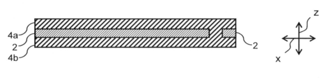
- FIG. 2 is a process cross-sectional view of the thin film transistor manufacturing method according to the embodiment of the present invention.
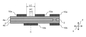
- FIG. 3 is a process cross-sectional view of the method of manufacturing the thin film transistor according to the embodiment of the present invention.
- FIG. 4 is a process sectional view of the method of manufacturing the thin film transistor according to the embodiment of the present invention.
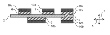
- FIG. 5 is a process cross-sectional view of the thin film transistor manufacturing method according to the embodiment of the present invention.
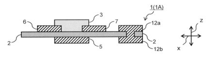
- FIG. 6 is a process cross-sectional view of the method for manufacturing the thin film transistor according to the embodiment of the present invention.
- FIG. 1 is a process sectional view of a method of manufacturing a thin film transistor according to an embodiment of the present invention.
- FIG. 2 is a process cross-sectional view of the thin film transistor manufacturing method according to the embodiment of the present invention.
- FIG. 3 is a
- FIG. 7 is a sectional view showing another example of the thin film transistor according to the embodiment of the present invention.
- FIG. 8 is a sectional view showing another example of the thin film transistor according to the embodiment of the present invention.
- FIG. 9 is a schematic diagram showing a configuration of a CMOS circuit.
- FIG. 10 is a sectional view showing another example of the thin film transistor according to the embodiment of the present invention.
- FIG. 11 is a process cross-sectional view of the method for manufacturing the thin film transistor according to the reference example.
- FIG. 12 is a process cross-sectional view of the method for manufacturing the thin film transistor according to the reference example.
- FIG. 13 is a process cross-sectional view of the method for manufacturing the thin film transistor according to the reference example.
- FIG. 11 is a process cross-sectional view of the method for manufacturing the thin film transistor according to the reference example.
- FIG. 14 is a process cross-sectional view of the method for manufacturing the thin film transistor according to the reference example.
- FIG. 15 is a process cross-sectional view of the method for manufacturing the thin film transistor according to the reference example.
- FIG. 16 is a process cross-sectional view of the method for manufacturing the thin film transistor according to the reference example.
- FIG. 17 is a process cross-sectional view of the method for manufacturing the thin film transistor according to the reference example.
- the method for producing a thin film transistor of the present invention includes (1) a step of forming a first conductive layer on one main surface of a substrate and forming a second conductive layer on the other main surface of the substrate; 2) a step of collectively forming a mask layer on the first conductive layer and the second conductive layer; and (3) a step of bringing the first conductive layer and the second conductive layer into contact with an etching solution in a lump Forming a source electrode and a drain electrode on one main surface of the base material by removing a partial region of the conductive layer and the second conductive layer, and forming a gate electrode on the other main surface of the base material And (4) forming an organic semiconductor layer on one main surface of the substrate from which the first conductive layer has been removed.
- the method for manufacturing a thin film transistor of the present invention includes a step of forming a mask layer collectively on the first conductive layer and the second conductive layer, even if the base material is thermally stretched or contracted, the source electrode It becomes easy to maintain the positional relationship between the drain electrode and the gate electrode. As a result, it is possible to suppress degradation in the performance of the transistor due to the displacement of the gate electrode with respect to the source electrode and the drain electrode.
- the base material also serves as a gate insulating film, it is not necessary to separately provide a gate insulating film such as a silicon oxide film, and the thickness of the entire transistor can be suppressed.
- the channel length can be controlled to 10 ⁇ m or less, and the circuit can be miniaturized.
- the thin film transistor of the present invention includes a first gate electrode formed on one main surface of the base material, a first source electrode, a first drain electrode formed on the other main surface of the base material, And a first transistor having a first organic semiconductor layer; a second gate electrode formed on the other main surface of the substrate; and a second source electrode formed on the one main surface of the substrate , A second transistor having a second drain electrode and a second organic semiconductor layer.
- the base material also serves as a gate insulating film, it is not necessary to separately provide a gate insulating film such as a silicon oxide film, and the thickness of the entire transistor can be suppressed.
- the thin film transistor of the present invention two transistors are arranged in different directions with a base material interposed therebetween, so that the arrangement interval between adjacent transistors can be reduced and the degree of circuit integration can be increased.
- the thin film transistor has a thickness direction and a plane direction.
- the thickness direction of the thin film transistor is a direction in which the organic semiconductor layer and the conductive layer are stacked on the substrate, and corresponds to the vertical direction in the drawing of the present application.
- the surface direction of the thin film transistor is a direction orthogonal to the thickness direction, and has a vertical direction and a horizontal direction. Note that the left-right direction in the drawing of the present application corresponds to the lateral direction of the surface direction of the thin film transistor.
- the base material also serves as a gate insulating film.
- the substrate is preferably formed from a polymer film such as polyethylene naphthalate (PEN), polyethylene terephthalate (PET), polyimide (PI), or the like. Since the mobility of the organic semiconductor is about 1 to 10 cm 2 / V ⁇ sec, the number of carriers moving between the source electrode and the drain electrode per unit time decreases if the thickness of the substrate is too large. On the other hand, if the film thickness of the base material is too small, the base material is broken or broken during the manufacture of the transistor, making it difficult to handle the base material. For this reason, the thickness of the substrate is preferably from 0.1 ⁇ m to 10 ⁇ m, more preferably from 1 ⁇ m to 7 ⁇ m, and even more preferably from 3 ⁇ m to 5 ⁇ m.
- PEN polyethylene naphthalate
- PET polyethylene terephthalate
- PI polyimide
- the organic semiconductor layer functions as a channel region of the transistor.
- a material for the organic semiconductor layer for example, pentacene, anthracene, tetracene, rubrene, polyacetylene, polythiophene, fullerene, carbon nanotube, or the like can be used.
- the first conductive layer and the second conductive layer are for forming respective electrodes such as a gate electrode, a source electrode, a drain electrode, a terminal electrode, and a via electrode constituting the transistor.
- electrodes such as a gate electrode, a source electrode, a drain electrode, a terminal electrode, and a via electrode constituting the transistor.
- the details will be described later with reference to an example of a manufacturing method.
- the first conductive layer and the second conductive layer for example, a conductive material such as Al, Ag, C, Ni, Au, or Cu can be used. Especially, it is preferable that the 1st conductive layer and the 2nd conductive layer are comprised from Cu. This is because Cu has high electrical conductivity, is inexpensive, and has excellent heat resistance.
- FIG. 1 to 6 are process cross-sectional views illustrating a part of the method of manufacturing the thin film transistor according to the present embodiment.
- Step of forming a first conductive layer on one main surface of a base material and forming a second conductive layer on the other main surface of the base material A polyimide film having a thickness of 3 ⁇ m is prepared as the base material 2 To do. As shown in FIG. 1, in order to form a terminal electrode and a via electrode, you may form the through-hole 11a which penetrates the base material 2 in the thickness direction z. Punching, laser processing, or the like can be used to form the through hole 11a.
- the first conductive layer 4 a is formed on one main surface of the substrate 2, and the second conductive layer 4 b is formed on the other main surface of the substrate 2.
- the first conductive layer 4 a is formed on the upper surface of the substrate 2 in the thickness direction z
- the second conductive layer 4 b is formed on the lower surface of the substrate 2.
- the method for forming the first conductive layer 4a and the second conductive layer 4b is not particularly limited, and for example, a vacuum deposition method or a sputtering method can be used.
- the through-hole 11a penetrating in the thickness direction z is not formed in the base material 2
- the first conductive layer 4a and the second conductive layer 4b are formed by attaching a conductive material formed in a foil shape. You can also
- Step of collectively forming a mask layer on the first conductive layer and the second conductive layer As shown in FIG. 3, a mask for determining the formation positions of the gate electrode, the source electrode, and the drain electrode
- the layers 10a and 10b are collectively formed on the first conductive layer 4a and the second conductive layer 4b, respectively.
- the mask layers 10a and 10b are formed as follows.
- a photosensitive resin such as a dry film resist or a liquid resist is applied on the first conductive layer 4a and the second conductive layer 4b.
- the photosensitive resin includes a negative type in which the exposed portion is insoluble in the developer and a positive type in which the exposed portion is soluble in the developer.
- a negative photosensitive resin is taken as an example. explain.
- a first resist is applied on the first conductive layer 4a, and a second resist is applied on the second conductive layer 4b.
- a predetermined circuit shape is drawn on the first resist and the second resist by irradiating an electron beam or light (ultraviolet rays) on the first resist and the second resist. At least the shape of the source electrode and the drain electrode is drawn on the first resist, and at least the shape of the gate electrode is drawn on the second resist.
- the center line C in the left-right direction x of the gate electrode formed by the mask layer 10b is a region between the source electrode and the drain electrode formed by the mask layer 10a. It is preferable that the channel length LC is located in the central region AC when the channel length LC is divided into three equal parts in the left-right direction x.
- the channel length LC is preferably 20 ⁇ m or less, more preferably 15 ⁇ m or less, and even more preferably 10 ⁇ m or less. The shorter the channel length LC, the higher the transistor processing speed.
- both the first resist and the second resist are exposed at once, whereby the first resist and the second resist are exposed.
- the circuit shape is transferred and baked.
- the unexposed portion of each resist is dissolved in the developer.
- the exposed portions of the first resist and the second resist remain on the first conductive layer 4a and the second conductive layer 4b as the mask layers 10a and 10b.
- the mask layer 10 (10a, 10b) can be formed of a dry film resist or a liquid resist, but is preferably formed of a dry film resist. Compared with the case where the mask layer 10 is formed of a liquid resist, it is not necessary to dry the solvent after applying the resist, so that productivity can be improved.
- the mask layers 10a and 10b are removed by bringing the mask layers 10a and 10b into contact with the stripping solution and dissolving them. As a result, as shown in FIG. 5, the source electrode 6 and the drain electrode 7 are formed on one main surface of the substrate 2, and the gate electrode 5 is formed on the other main surface of the substrate 2. Further, by removing the mask layers 10 a and 10 b, the terminal electrode 12 a is formed on one main surface of the substrate 2, and the terminal electrode 12 b is formed on the other main surface of the substrate 2.
- the terminal electrodes 12a and 12b are conductive.
- the source electrode 6, the drain electrode 7, and the gate electrode 5 are formed by batch photolithography and batch wet etching. For this reason, even if the base material 2 is thermally stretched or thermally contracted, the positional relationship among the source electrode 6, the drain electrode 7, and the gate electrode 5 can be easily maintained. As a result, the performance degradation of the thin film transistor due to the positional deviation of the gate electrode 5 with respect to the source electrode 6 and the drain electrode 7 can be suppressed.
- Step of forming an organic semiconductor layer on one main surface of the base material from which the first conductive layer has been removed As shown in FIG. 6, one main surface of the base material 2 from which the first conductive layer 4a has been removed An organic semiconductor layer 3 is formed on the surface. In FIG. 6, on one main surface of the base material 2 from which the first conductive layer 4 a has been removed, on at least some main surfaces of the source electrode 6, and on at least some main surfaces of the drain electrode 7. An organic semiconductor layer 3 is formed. As a method of forming the organic semiconductor layer 3, for example, vapor deposition, ink jet, or dispenser can be used. Through the above operation, the thin film transistor 1 (1A) is manufactured.
- FIGS. 7 to 10 are cross-sectional views of the thin film transistor in the thickness direction z.
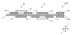
- the thin film transistor 1 (1 ⁇ / b> B) of the present invention is formed on the first main electrode 5 a formed on one main surface of the substrate 2 and on the other main surface of the substrate 2.
- a first transistor 20 having a first source electrode 6a, a first drain electrode 7a, and a first organic semiconductor layer 3a; a second gate electrode 5b formed on the other main surface of the substrate 2;
- a second transistor 21 having a second source electrode 6b, a second drain electrode 7b, and a second organic semiconductor layer 3b formed on one main surface of the substrate 2.
- the first gate electrode 5a of the first transistor 20 is formed between the first source electrode 6a and the first drain electrode 7a, and the second gate electrode 5b of the second transistor 21 is connected to the second source electrode 6b and the second source electrode 6b. It is formed between the two drain electrodes 7b.
- the thin film transistor 1B of the present invention since the first transistor 20 and the second transistor 21 are arranged in different directions with the base material 2 interposed therebetween, the arrangement interval between adjacent transistors can be reduced, The degree of circuit integration can be increased.
- the first gate electrode 5a, the first source electrode 6a, the first drain electrode 7a, the second gate electrode 5b, the second source electrode 6b, and the second drain electrode 7b are formed by batch photolithography and batch wet etching. It is preferable. Even if the substrate 2 is thermally stretched or contracted, the first gate electrode 5a, the first source electrode 6a, the first drain electrode 7a; the second gate electrode 5b, the second source electrode 6b, the second drain electrode 7b; It becomes easy to maintain each positional relationship. As a result, the displacement of the first gate electrode 5a with respect to the first source electrode 6a and the first drain electrode 7a and the displacement of the second gate electrode 5b with respect to the second source electrode 6b and the second drain electrode 7b are caused. Performance degradation can be suppressed.
- a plurality of transistors can be manufactured as in the case of manufacturing one transistor, so that productivity can be improved. it can.
- the first source electrode 6a or the first drain electrode 7a and the second source electrode 6b or the second drain electrode 7b are arranged to overlap each other.
- the first transistor 20 and the second transistor 21 in this manner, the arrangement interval between adjacent transistors can be further reduced.
- the first drain electrode 7a and the second source electrode 6b are arranged so as to overlap each other, but the first source electrode 6a and the second source electrode 6b are arranged in accordance with the conductivity type of the semiconductor and the type of circuit.
- the two source electrodes 6b may be arranged to overlap each other, the first source electrode 6a and the second drain electrode 7b may be arranged to overlap each other, or the first drain electrode 7a and the second drain electrode 7b may overlap each other. May be arranged.
- the conductivity type of the first organic semiconductor layer 3a and the conductivity type of the second organic semiconductor layer 3b have opposite polarities, and the first transistor 20 and the second transistor 21 are configured to be complementary. Thereby, the first transistor 20 and the second transistor 21 can be arranged in a CMOS structure called a metal oxide semiconductor (MOS).
- MOS metal oxide semiconductor
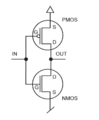
- FIG. 9 is a schematic diagram showing the configuration of a CMOS circuit.
- a CMOS has a circuit configuration in which PMOS and NMOS are paired and the operation characteristics of the PMOS and NMOS are complementarily combined, and can be operated at a low voltage, so that power consumption can be suppressed.
- G represents a gate
- S represents a source
- D represents a drain
- IN represents an input
- OUT represents an output.
- the conductivity type of the first organic semiconductor layer 3a and the conductivity type of the second organic semiconductor layer 3b may be of opposite polarities.
- the first organic semiconductor layer 3a is p-type and the second organic semiconductor layer 3b is n-type.
- the first organic semiconductor layer 3a may be n-type and the second organic semiconductor layer 3b may be p-type.
- first organic semiconductor layer 3a and the second organic semiconductor layer for example, tetracene, pentacene, anthracene, rubrene, polyacetylene, polythiophene, fullerene, carbon nanotubes and the like can be used in the same manner as the organic semiconductor layer described above.
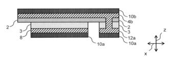
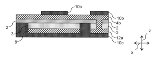
- the thin film transistor is as follows: Can also be configured. That is, as shown in FIG. 10, the thin film transistor 1 (1D) is arranged in a region where the first drain electrode 7a and the second drain electrode 7b overlap and the first drain electrode 7a and the second drain electrode 7b overlap. It is preferable that a through hole 11b is formed in the thickness direction of the material 2 and the first drain electrode 7a and the second drain electrode 7b are connected through the through hole 11b. The through hole 11b is provided separately from the through hole 11a for conducting the terminal electrodes 12a and 12b.
- the arrangement interval between the first transistor 20 and the second transistor 21 in the horizontal direction x in FIG. 10 can be reduced. Further, since the first drain electrode 5a and the second drain electrode 5b are connected in the through hole 11b, the wiring length for connecting the first drain electrode 5a and the second drain electrode 5b can be shortened. It is not necessary to secure a space for wiring. Similar to the through holes 11a for forming the terminal electrodes 12a, 12b and the via electrodes, the through holes 11b can be formed by punching, laser processing, or the like.
- FIGS. 11 to 17 are process cross-sectional views of the thin film transistor manufacturing method according to the reference example.
- the organic semiconductor layer 3 is formed on one main surface of the substrate 2, the first conductive layer 4 a is formed on the organic semiconductor layer 3, and the second conductive surface is formed on the other main surface of the substrate 2.
- Conductive layer 4b is formed.
- the organic semiconductor layer 3 is formed by a vacuum deposition method.
- the first conductive layer 4a and the second conductive layer 4b are formed by a vacuum deposition method or a sputtering method.
- Mask layers 10 (10a, 10b) are formed on the first conductive layer 4a and the second conductive layer 4b, respectively.
- the mask layer 10 is for forming an electrode. For example, after applying and drying a photoresist on the first conductive layer 4a, the circuit shape is transferred to the photoresist using an exposure device, and finally unnecessary. It is formed by dissolving and removing the resist with a developing solution. Further, the mask layer 10b is formed to cover the entire surface of the second conductive layer 4b so that the second conductive layer 4b is not etched.
- the organic semiconductor layer 3 and the first conductive layer 4a are etched using an etchant.
- the source / drain electrode 8 that is, the electrode in which the source electrode and the drain electrode are connected
- the terminal electrode 12a are formed.
- a mask layer 10 c is formed on one main surface of the source / drain electrode 8, the terminal electrode 12 a, and the base material 2.
- the circuit shape is transferred to the mask layer 10b (photoresist) using an exposure apparatus, and finally unnecessary resist is dissolved and removed with a developer (see FIG. 13).
- the second conductive layer 4b is etched using an etching solution. Thereby, as shown in FIG. 14, the gate electrode 5 and the terminal electrode 12b are formed. Since the mask layer 10c is formed on the source / drain electrode 8 and the terminal electrode 12a, these electrodes are not etched.
- the mask layers 10b and 10c are peeled and removed by bringing the mask layers 10b and 10c into contact with a stripping solution and dissolving.
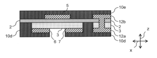
- a mask layer 10d is formed on the source / drain electrode 8 (on the first conductive layer 4a). At this time, the mask layer 10d is formed so as to cover the terminal electrode 12a so that the terminal electrode 12a is not etched.
- the mask layer 10e is formed so as to cover the gate electrode 5 and the terminal electrode 12b so that the gate electrode 5 and the terminal electrode 12b are not etched.
- a source electrode 6 and a drain electrode 7 are formed on the organic semiconductor layer 3 as shown in FIG.
- the mask layers 10d and 10e are dissolved by being brought into contact with a stripping solution, and the mask layers 10d and 10e are stripped and removed to form a thin film transistor.
- the thin film transistor manufacturing method according to the reference example is formed with a mask layer 10 b for forming the gate electrode 5 and a mask layer 10 d for forming the source electrode 6 and the drain electrode 7.
Landscapes
- Engineering & Computer Science (AREA)
- Manufacturing & Machinery (AREA)
- Thin Film Transistor (AREA)
- Electroluminescent Light Sources (AREA)
- Electrodes Of Semiconductors (AREA)
- Internal Circuitry In Semiconductor Integrated Circuit Devices (AREA)
- Metal-Oxide And Bipolar Metal-Oxide Semiconductor Integrated Circuits (AREA)
Abstract
【課題】性能の低下およびバラツキを抑えることができる薄膜トランジスタの製造方法と、薄膜トランジスタを提供する。 【解決手段】本発明の薄膜トランジスタ1(1A)の製造方法は、基材2の一方の主面上に第1導電層を形成して、基材2の他方の主面上に第2導電層を形成する工程と、第1導電層および第2導電層の上にマスク層を一括して形成する工程と、第1導電層および第2導電層を一括してエッチング液に接触させて、第1導電層および第2導電層の一部領域を除去することにより、基材2の一方の主面上にソース電極6とドレイン電極7を形成し、基材2の他方の主面上にゲート電極5を形成する工程と、第1導電層が除去された基材2の一方の主面上に有機物半導体層3を形成する工程と、を含む。
Description
本発明は、半導体層に有機物半導体を用いた薄膜トランジスタに関するものである。
近年、トランジスタの薄型化、フレキシブル化、軽量化等の要望が高まるにつれて、基材材料としてはポリエチレンナフタレート(PEN)やポリイミド(PI)等の高分子フィルムが使用されている。これに伴い、半導体層としては、当該フィルムの耐熱温度以下で成膜が可能な有機物半導体が用いられている。また、薄膜トランジスタを構成するソース電極、ドレイン電極、ゲート電極の作製には、フォトリソグラフィ法や印刷法が用いられている。
特許文献1には、ゲート絶縁膜を基板(基材)として用い、各電極や半導体層を印刷法によって形成した薄膜トランジスタが記載されている。
トランジスタの製造では成膜や熱処理などの熱プロセスが繰り返し行われる。例えば、スパッタや蒸着などの真空成膜や塗布プロセス後の乾燥などである。このような熱プロセスに伴い、基材が延伸或いは収縮して、基材の寸法が変化することがある。フォトリソグラフィ法でトランジスタを製造するときには、各層の成膜やマスク層を形成するための露光処理等を層ごとに行うため、各層の形成時にそれぞれ熱処理がなされて、基材の寸法が工程毎に変化することがあった。このため、ゲート電極に対するソース電極およびドレイン電極の形成位置を制御するのが困難であった。その結果、設計通りのトランジスタが作製できず、トランジスタの性能にバラツキが生じて製品の歩留まりが悪化することがあった。
そこで、本発明は、性能の低下およびバラツキを抑えることができる薄膜トランジスタの製造方法と、薄膜トランジスタを提供することを目的とする。
上記目的を達成し得た本発明の薄膜トランジスタの製造方法は、基材の一方の主面上に第1導電層を形成して、基材の他方の主面上に第2導電層を形成する工程と、第1導電層および第2導電層の上にマスク層を一括して形成する工程と、第1導電層および第2導電層を一括してエッチング液に接触させて、第1導電層および第2導電層の一部領域を除去することにより、基材の一方の主面上にソース電極とドレイン電極を形成し、基材の他方の主面上にゲート電極を形成する工程と、第1導電層が除去された基材の一方の主面上に有機物半導体層を形成する工程と、を含む点に要旨を有するものである。本発明の薄膜トランジスタの製造方法は、第1導電層および第2導電層の上にマスク層を一括して形成する工程を含んでいるため、基材が熱延伸或いは熱収縮しても、ソース電極、ドレイン電極、ゲート電極の位置関係を維持しやすくなる。その結果、ソース電極およびドレイン電極に対するゲート電極の位置ズレに起因するトランジスタの性能低下を抑えることができる。また、本発明の薄膜トランジスタの製造方法は、基材がゲート絶縁膜を兼ねているため、シリコン酸化膜等のゲート絶縁膜を別途設ける必要がなく、トランジスタ全体の厚みを抑えることができる。これにより、ゲート絶縁膜のピンホールの発生や膜厚などの品質のバラツキに起因するトランジスタの性能のバラツキが発生しない。さらに、本発明の薄膜トランジスタの製造方法ではフォトリソグラフィ法によってソース電極、ドレイン電極、ゲート電極を形成するため、チャネル長を10μm以下に制御することができ、回路の微細化が可能である。
本発明の薄膜トランジスタの製造方法において、第1導電層および第2導電層が、Cuから構成されていることが好ましい。Cuは高い電気伝導性を有しているとともに、安価であり、耐熱性にも優れているからである。
本発明の薄膜トランジスタの製造方法において、マスク層がドライフィルムレジストで形成されていることが好ましい。マスク層が液体レジストで形成されている場合と比較して、マスク層がドライフィルムレジストで形成されている場合にはレジストを塗布した後の溶剤乾燥が不要なため、生産性を高めることができる。
また、上記目的を達成し得た本発明の薄膜トランジスタは、基材の一方の主面上に形成されている第1ゲート電極と、基材の他方の主面上に形成されている第1ソース電極、第1ドレイン電極、および第1有機物半導体層とを有する第1トランジスタと;基材の他方の主面上に形成されている第2ゲート電極と、基材の一方の主面上に形成されている第2ソース電極、第2ドレイン電極、および第2有機物半導体層とを有する第2トランジスタと;を含む点を要旨とする。本発明の薄膜トランジスタは、基材がゲート絶縁膜を兼ねているため、シリコン酸化膜等のゲート絶縁膜を別途設ける必要がなく、トランジスタ全体の厚みを抑えることができる。また、ゲート絶縁膜のピンホールの発生や膜厚などの品質のバラツキに起因するトランジスタの性能のバラツキが発生しない。本発明の薄膜トランジスタは、基材を挟んで互いに異なる向きに2つのトランジスタが配置されているため、隣り合うトランジスタ同士の配置間隔を狭めることができ、回路の集積度を高められる。
第1ゲート電極、第1ソース電極、第1ドレイン電極と、第2ゲート電極、第2ソース電極、第2ドレイン電極が、一括したフォトリソグラフィおよび一括したウェットエッチングにより形成されていることが好ましい。本発明の薄膜トランジスタではフォトリソグラフィ法によって各電極が形成されているため、チャネル長を10μm以下に制御することができ、回路の微細化が可能である。また、各電極が一括したフォトリソグラフィおよび一括したウェットエッチングにより形成されているため、基材が熱延伸或いは熱収縮しても、ソース電極、ドレイン電極、ゲート電極の位置関係を維持しやすくなる。その結果、ソース電極およびドレイン電極に対するゲート電極の位置ズレに起因するトランジスタの性能低下を抑えることができる。
第1ソース電極または第1ドレイン電極と、第2ソース電極または第2ドレイン電極が重なって配置されていることが好ましい。隣り合うトランジスタ同士の配置間隔をさらに狭めることができるため、回路の集積度をより一層高められる。
第1有機物半導体層の導電型と第2有機物半導体層の導電型とは反対極性であり、第1トランジスタと第2トランジスタは相補型に構成されていることが好ましい。これにより、第1トランジスタと第2トランジスタを、金属酸化物半導体(MOS)でいうところのCMOS構造に配置することが可能である。
第1ドレイン電極と第2ドレイン電極が重なって配置され、第1ドレイン電極と第2ドレイン電極が重なる領域において、基材に貫通孔が形成されており、貫通孔を通じて第1ドレイン電極と第2ドレイン電極が接続されていることが好ましい。第1ドレイン電極と第2ドレイン電極が貫通孔と重なって配置されているため、隣り合うトランジスタ同士の配置間隔をさらに狭めることができ、回路の集積度をより一層高められる。また、貫通孔において、第1ドレイン電極と第2ドレイン電極が接続されているため、第1ドレイン電極と第2ドレイン電極の接続に必要な配線長を短くできるとともに、配線のための空間を別途確保する必要がない。
基材が高分子フィルムから形成されており、基材の厚みが0.1μm以上10μm以下であることが好ましい。基材が膜厚0.1μm以上10μm以下の高分子フィルムであれば、単位時間当たりにチャネル領域を移動するキャリア数を確保しつつ、製造時に基材を取り扱いやすくなる。
本発明の薄膜トランジスタの製造方法では、基材が熱延伸或いは熱収縮しても、ソース電極、ドレイン電極、ゲート電極の位置関係を維持しやすくなる。その結果、ソース電極およびドレイン電極に対するゲート電極の位置ズレに起因するトランジスタの性能低下を抑えることができる。また、本発明の薄膜トランジスタの製造方法は、チャネル長を10μm以下に制御することができ、回路の微細化が可能である。
本発明の薄膜トランジスタの製造方法および薄膜トランジスタは、基材がゲート絶縁膜を兼ねているため、シリコン酸化膜等のゲート絶縁膜を別途設ける必要がなく、トランジスタ全体の厚みを抑えることができる。これにより、ゲート絶縁膜のピンホールの発生や膜厚などの品質のバラツキに起因するトランジスタの性能のバラツキが発生しない。
さらに、第1トランジスタおよび第2トランジスタを含む本発明の薄膜トランジスタは基材を挟んで互いに異なる向きに2つのトランジスタが配置されているため、隣り合うトランジスタ同士の配置間隔を狭めることができ、回路の集積度を高められる。
本発明の薄膜トランジスタの製造方法および薄膜トランジスタは、基材がゲート絶縁膜を兼ねているため、シリコン酸化膜等のゲート絶縁膜を別途設ける必要がなく、トランジスタ全体の厚みを抑えることができる。これにより、ゲート絶縁膜のピンホールの発生や膜厚などの品質のバラツキに起因するトランジスタの性能のバラツキが発生しない。
さらに、第1トランジスタおよび第2トランジスタを含む本発明の薄膜トランジスタは基材を挟んで互いに異なる向きに2つのトランジスタが配置されているため、隣り合うトランジスタ同士の配置間隔を狭めることができ、回路の集積度を高められる。
以下、実施の形態に基づき本発明をより具体的に説明するが、本発明はもとより下記実施の形態によって制限を受けるものではなく、前・後記の趣旨に適合し得る範囲で変更を加えて実施することも勿論可能であり、それらはいずれも本発明の技術的範囲に包含される。また、図面における種々部材の寸法比は、本発明の特徴を理解に資することを優先しているため、実際の寸法比とは異なる場合がある。
本発明の薄膜トランジスタの製造方法は、(1)基材の一方の主面上に第1導電層を形成して、基材の他方の主面上に第2導電層を形成する工程と、(2)第1導電層および第2導電層の上にマスク層を一括して形成する工程と、(3)第1導電層および第2導電層を一括してエッチング液に接触させて、第1導電層および第2導電層の一部領域を除去することにより、基材の一方の主面上にソース電極とドレイン電極を形成し、基材の他方の主面上にゲート電極を形成する工程と、(4)第1導電層が除去された基材の一方の主面上に有機物半導体層を形成する工程と、を含むものである。本発明の薄膜トランジスタの製造方法は、第1導電層および第2導電層の上にマスク層を一括して形成する工程を含んでいるため、基材が熱延伸或いは熱収縮しても、ソース電極、ドレイン電極、ゲート電極の位置関係を維持しやすくなる。その結果、ソース電極およびドレイン電極に対するゲート電極の位置ズレに起因するトランジスタの性能低下を抑えることができる。また、本発明の薄膜トランジスタの製造方法は、基材がゲート絶縁膜を兼ねているため、シリコン酸化膜等のゲート絶縁膜を別途設ける必要がなく、トランジスタ全体の厚みを抑えることができる。これにより、ゲート絶縁膜のピンホールの発生や膜厚などの品質のバラツキに起因するトランジスタの性能のバラツキが発生しない。さらに、本発明の薄膜トランジスタの製造方法ではフォトリソグラフィ法によってソース電極、ドレイン電極、ゲート電極を形成するため、チャネル長を10μm以下に制御することができ、回路の微細化が可能である。
また、本発明の薄膜トランジスタは、基材の一方の主面上に形成されている第1ゲート電極と、基材の他方の主面上に形成されている第1ソース電極、第1ドレイン電極、および第1有機物半導体層とを有する第1トランジスタと;基材の他方の主面上に形成されている第2ゲート電極と、基材の一方の主面上に形成されている第2ソース電極、第2ドレイン電極、および第2有機物半導体層とを有する第2トランジスタと;を含むものである。本発明の薄膜トランジスタは、基材がゲート絶縁膜を兼ねているため、シリコン酸化膜等のゲート絶縁膜を別途設ける必要がなく、トランジスタ全体の厚みを抑えることができる。また、ゲート絶縁膜のピンホールの発生や膜厚などの品質のバラツキに起因するトランジスタの性能のバラツキが発生しない。さらに、本発明の薄膜トランジスタは、基材を挟んで互いに異なる向きに2つのトランジスタが配置されているため、隣り合うトランジスタ同士の配置間隔を狭めることができ、回路の集積度を高められる。
本発明において、薄膜トランジスタは厚み方向と面方向を有する。薄膜トランジスタの厚み方向は、基材上に有機物半導体層や導電層が積層される方向であり、本願の図の上下方向に相当する。薄膜トランジスタの面方向は、厚み方向と直交する方向であり、縦方向と横方向を有している。なお、本願の図の左右方向は、薄膜トランジスタの面方向のうち、横方向に相当する。
基材は、ゲート絶縁膜を兼ねている。基材は、ポリエチレンナフタレート(PEN)、ポリエチレンテレフタレート(PET)、ポリイミド(PI)等の高分子フィルムから形成されることが好ましい。有機物半導体の移動度は1~10cm2/V・sec程度であることから、基材の膜厚が大きすぎると単位時間当たりにソース電極とドレイン電極の間を移動するキャリア数が減少する。他方、基材の膜厚が小さすぎると、トランジスタの製造時に基材が折れたり、壊れたりするなどして、基材が取り扱いにくくなる。このため、基材の厚みは0.1μm以上10μm以下であることが好ましく、1μm以上7μm以下であることがより好ましく、3μm以上5μm以下であることがさらに好ましい。
有機物半導体層は、トランジスタのチャネル領域として機能する。有機物半導体層の材料としては、例えば、ペンタセン、アントラセン、テトラセン、ルブレン、ポリアセチレン、ポリチオフェン、フラーレン、カーボンナノチューブ等を用いることができる。
第1導電層と第2導電層は、トランジスタを構成するゲート電極、ソース電極、ドレイン電極、端子電極、ビア電極等の各電極を形成するためのものである。詳細は製造方法の例を挙げて後述するが、第1導電層および第2導電層の一部の領域をマスク層によって覆い、第1導電層および第2導電層をエッチング液に接触させることにより、各電極を形成することができる。
第1導電層と第2導電層は、例えば、Al、Ag、C、Ni、Au、Cu等の導電性材料を用いることができる。中でも、第1導電層および第2導電層は、Cuから構成されていることが好ましい。Cuは高い電気伝導性を有しているとともに、安価であり、耐熱性にも優れているからである。
以下、本実施の形態に係る薄膜トランジスタの製造方法の好ましい例について、図面を用いて詳細に説明する。図1~図6は、本実施の形態に係る薄膜トランジスタの製造方法の一部を示す工程断面図である。
(1)基材の一方の主面上に第1導電層を形成して、基材の他方の主面上に第2導電層を形成する工程
膜厚3μmのポリイミドフィルムを基材2として準備する。図1に示すように、端子電極やビア電極を形成するために、基材2を厚み方向zに貫通する貫通孔11aを形成してもよい。貫通孔11aの形成には、パンチング、レーザー加工等を用いることができる。
膜厚3μmのポリイミドフィルムを基材2として準備する。図1に示すように、端子電極やビア電極を形成するために、基材2を厚み方向zに貫通する貫通孔11aを形成してもよい。貫通孔11aの形成には、パンチング、レーザー加工等を用いることができる。
図2に示すように、基材2の一方の主面上に第1導電層4aを形成して、基材2の他方の主面上に第2導電層4bを形成する。図2においては、基材2の厚み方向zの上側の面上に第1導電層4aが形成され、基材2の下側の面上に第2導電層4bが形成されている。第1導電層4aおよび第2導電層4bを成膜する方法は特に限定されず、例えば、真空蒸着法やスパッタリング法を用いることができる。また、基材2に厚み方向zに貫通する貫通孔11aが形成されない場合には、箔状に形成された導電性材料を貼り付けることにより第1導電層4aおよび第2導電層4bを成膜することもできる。
(2)第1導電層および第2導電層の上にマスク層を一括して形成する工程
図3に示すように、ゲート電極、ソース電極、ドレイン電極の各電極の形成位置を決めるためのマスク層10a、10bをそれぞれ第1導電層4a、第2導電層4bの上に一括して形成する。
図3に示すように、ゲート電極、ソース電極、ドレイン電極の各電極の形成位置を決めるためのマスク層10a、10bをそれぞれ第1導電層4a、第2導電層4bの上に一括して形成する。
具体的には、マスク層10a、10bの形成は次のように行う。第1導電層4aおよび第2導電層4bの上に、ドライフィルムレジストや液体レジスト等の感光性樹脂を塗布する。感光性樹脂には、露光部分が現像液に対して不溶性となるネガ型と、露光部分が現像液に対して可溶性となるポジ型があるが、以下ではネガ型の感光性樹脂を例にして説明する。第1導電層4aの上には第1レジストが塗布され、第2導電層4bの上には第2レジストが塗布される。第1レジスト、第2レジストの上から電子ビームや光(紫外線)を照射して、第1レジストおよび第2レジストに所定の回路形状を描画する。第1レジストには、少なくともソース電極とドレイン電極の形状が描画され、第2レジストには少なくともゲート電極の形状が描画される。
トランジスタの性能低下を抑止するために、図3に示すように、マスク層10bが形成するゲート電極の左右方向xにおける中心線Cが、マスク層10aが形成するソース電極とドレイン電極の間の領域(チャネル長LC)を左右方向xに三等分割した場合の中央領域ACに位置していることが好ましい。
チャネル長LCは20μm以下であることが好ましく、15μm以下であることがより好ましく、10μm以下であることがさらに好ましい。チャネル長LCが短いほど、トランジスタの処理速度を高めることができる。
基材2の両面から一括して露光可能な露光装置(図示していない)を用いて、第1レジストと、第2レジストの両方を一括して露光することによって、第1レジストと第2レジストに対して回路形状の転写、焼き付けを行う。
第1レジストと第2レジストに現像液を接触させることによって、各レジストの未露光部分は現像液に対して溶解する。その結果、第1レジストと第2レジストの露光部分がマスク層10a、10bとして第1導電層4aおよび第2導電層4b上に残る。
マスク層10(10a、10b)は、ドライフィルムレジストや液体レジストで形成することができるが、ドライフィルムレジストで形成されていることが好ましい。マスク層10が液体レジストで形成されている場合と比較して、レジストを塗布した後の溶剤乾燥が不要なため、生産性を高めることができる。
(3)第1導電層および第2導電層を一括してエッチング液に接触させて、第1導電層および第2導電層の一部領域を除去することにより、基材の一方の主面上にソース電極とドレイン電極を形成し、基材の他方の主面上にゲート電極を形成する工程
次に、マスク層10aが形成された第1導電層4aと、マスク層10bが形成された第2導電層4bを一括してエッチング液に接触させる。この操作によって、図4に示すように、第1導電層4aおよび第2導電層4bの一部領域が除去される。
次に、マスク層10aが形成された第1導電層4aと、マスク層10bが形成された第2導電層4bを一括してエッチング液に接触させる。この操作によって、図4に示すように、第1導電層4aおよび第2導電層4bの一部領域が除去される。
マスク層10a、10bを剥離液に接触させて溶解することにより、マスク層10a、10bを除去する。その結果、図5に示すように、基材2の一方の主面上にソース電極6とドレイン電極7が形成され、基材2の他方の主面上にはゲート電極5が形成される。また、マスク層10a、10bを除去することにより、基材2の一方の主面上には端子電極12aが形成され、基材2の他方の主面上には端子電極12bが形成される。なお、端子電極12a、12bは導通している。
図5に示すように、本発明の薄膜トランジスタは、ソース電極6と、ドレイン電極7と、ゲート電極5が一括したフォトリソグラフィおよび一括したウェットエッチングにより形成されている。このため、基材2が熱延伸或いは熱収縮しても、ソース電極6、ドレイン電極7、ゲート電極5の位置関係を維持しやすくなる。その結果、ソース電極6およびドレイン電極7に対するゲート電極5の位置ズレに起因する薄膜トランジスタの性能低下を抑えることができる。
(4)第1導電層が除去された基材の一方の主面上に有機物半導体層を形成する工程
図6に示すように、第1導電層4aが除去された基材2の一方の主面上に有機物半導体層3を形成する。図6においては、第1導電層4aが除去された基材2の一方の主面上と、ソース電極6の少なくとも一部の主面上と、ドレイン電極7の少なくとも一部の主面上に有機物半導体層3が形成されている。有機物半導体層3を形成する方法は、例えば、蒸着、インクジェット、ディスペンサーを用いることができる。以上の操作により、薄膜トランジスタ1(1A)が製造される。
図6に示すように、第1導電層4aが除去された基材2の一方の主面上に有機物半導体層3を形成する。図6においては、第1導電層4aが除去された基材2の一方の主面上と、ソース電極6の少なくとも一部の主面上と、ドレイン電極7の少なくとも一部の主面上に有機物半導体層3が形成されている。有機物半導体層3を形成する方法は、例えば、蒸着、インクジェット、ディスペンサーを用いることができる。以上の操作により、薄膜トランジスタ1(1A)が製造される。
次に、図6に示した薄膜トランジスタとは異なる態様の薄膜トランジスタについて、図7~図10を参照しながら説明する。なお図7~図10の説明において、上記の説明と重複する部分は説明を省略する。図7、図8、図10は、薄膜トランジスタの厚み方向zの断面図を表す。
図7に示すように、本発明の薄膜トランジスタ1(1B)は、基材2の一方の主面上に形成されている第1ゲート電極5aと、基材2の他方の主面上に形成されている第1ソース電極6a、第1ドレイン電極7a、および第1有機物半導体層3aとを有する第1トランジスタ20と;基材2の他方の主面上に形成されている第2ゲート電極5bと、基材2の一方の主面上に形成されている第2ソース電極6b、第2ドレイン電極7b、および第2有機物半導体層3bとを有する第2トランジスタ21と;を含むものである。
第1トランジスタ20の第1ゲート電極5aは、第1ソース電極6aと第1ドレイン電極7aの間に形成されており、第2トランジスタ21の第2ゲート電極5bは、第2ソース電極6bと第2ドレイン電極7bの間に形成されている。
このように、本発明の薄膜トランジスタ1Bは、基材2を挟んで互いに異なる向きに第1トランジスタ20と第2トランジスタ21が配置されているため、隣り合うトランジスタ同士の配置間隔を狭めることができ、回路の集積度を高められるものである。
第1ゲート電極5a、第1ソース電極6a、第1ドレイン電極7aと、第2ゲート電極5b、第2ソース電極6b、第2ドレイン電極7bが、一括したフォトリソグラフィおよび一括したウェットエッチングにより形成されていることが好ましい。基材2が熱延伸或いは熱収縮しても、第1ゲート電極5a、第1ソース電極6a、第1ドレイン電極7a;第2ゲート電極5b、第2ソース電極6b、第2ドレイン電極7b;の位置関係をそれぞれ維持しやすくなる。その結果、第1ソース電極6aおよび第1ドレイン電極7aに対する第1ゲート電極5aの位置ズレや、第2ソース電極6bおよび第2ドレイン電極7bに対する第2ゲート電極5bの位置ズレに起因するトランジスタの性能低下を抑えることができる。
本発明では、フォトリソグラフィ法でマスク層10に描画される回路形状を変更することによって、1つのトランジスタを作製する場合と同様に複数のトランジスタを作製することができるため、生産性を高めることができる。
回路の集積度をより一層高めるために、第1ソース電極6aまたは第1ドレイン電極7aと、第2ソース電極6bまたは第2ドレイン電極7bが重なって配置されていることが好ましい。このように第1トランジスタ20と第2トランジスタ21を構成することにより、隣り合うトランジスタ同士の配置間隔をさらに狭めることができる。図8に示す薄膜トランジスタ1(1C)では、第1ドレイン電極7aと第2ソース電極6bが重なって配置されているが、半導体の導電型や回路の種類に応じて、第1ソース電極6aと第2ソース電極6bが重なって配置されていてもよいし、第1ソース電極6aと第2ドレイン電極7bが重なって配置されていてもよいし、第1ドレイン電極7aと第2ドレイン電極7bが重なって配置されていてもよい。
第1有機物半導体層3aの導電型と第2有機物半導体層3bの導電型とは反対極性であり、第1トランジスタ20と第2トランジスタ21は相補型に構成されていることが好ましい。これにより、第1トランジスタ20と第2トランジスタ21を、金属酸化物半導体(MOS)でいうところのCMOS構造に配置することが可能である。
図9はCMOS回路の構成を示す模式図である。CMOSはPMOSとNMOSを一対とし、PMOSとNMOSの動作特性を相補的に組み合わせた回路構成であり、低電圧で動作が可能であることから消費電力を抑制できるという特徴を有している。図9において、Gはゲート、Sはソース、Dはドレイン、INは入力、OUTは出力を示している。
第1有機物半導体層3aの導電型と第2有機物半導体層3bの導電型は反対極性であればよく、第1有機物半導体層3aをp型にして第2有機物半導体層3bをn型にしてもよいし、第1有機物半導体層3aをn型にして第2有機物半導体層3bをp型にしてもよい。
第1有機物半導体層3aおよび第2有機物半導体層は、上述した有機物半導体層と同様に、例えば、テトラセン、ペンタセン、アントラセン、ルブレン、ポリアセチレン、ポリチオフェン、フラーレン、カーボンナノチューブ等を用いることができる。
第1有機物半導体層3aの導電型と第2有機物半導体層3bの導電型とは反対極性であり、第1トランジスタ20と第2トランジスタ21が相補型に構成されている場合、次のように薄膜トランジスタを構成することもできる。すなわち、図10に示すように、薄膜トランジスタ1(1D)は、第1ドレイン電極7aと第2ドレイン電極7bが重なって配置され、第1ドレイン電極7aと第2ドレイン電極7bが重なる領域において、基材2の厚み方向に貫通孔11bが形成されており、貫通孔11bを通じて第1ドレイン電極7aと第2ドレイン電極7bが接続されていることが好ましい。なお、貫通孔11bは、端子電極12a、12bを導通するための貫通孔11aとは別に設けられる。第1ドレイン電極7aと第2ドレイン電極7bが重なって配置されることによって、図10の左右方向xにおける第1トランジスタ20と第2トランジスタ21の配置間隔を狭めることができる。また、貫通孔11bにおいて、第1ドレイン電極5aと第2ドレイン電極5bが接続されているため、第1ドレイン電極5aと第2ドレイン電極5bを接続するための配線長を短くすることができ、配線のための空間を別途確保する必要もない。なお、端子電極12a、12bやビア電極を形成するための貫通孔11aと同様に、貫通孔11bは、パンチング、レーザー加工等により形成することができる。
(参考例)
参考として、マスク層を片面ずつ形成する場合の薄膜トランジスタの製造方法について、図11~図17を用いて説明する。図11~図17は、参考例にかかる薄膜トランジスタの製造方法の工程断面図である。
参考として、マスク層を片面ずつ形成する場合の薄膜トランジスタの製造方法について、図11~図17を用いて説明する。図11~図17は、参考例にかかる薄膜トランジスタの製造方法の工程断面図である。
図11には、基材2の一方の主面上に有機物半導体層3が形成され、有機物半導体層3上に第1導電層4aが形成され、基材2の他方の主面上に第2導電層4bが形成されている。有機物半導体層3の形成は、真空蒸着法によって行われる。また、第1導電層4a、第2導電層4bの形成は、真空蒸着法やスパッタリング法によって行われる。第1導電層4a上と、第2導電層4b上には、マスク層10(10a、10b)がそれぞれ形成されている。マスク層10は、電極を形成するためのものであり、例えば、第1導電層4a上にフォトレジストを塗布・乾燥後に、露光装置を用いてフォトレジストに回路形状を転写し、最後に不要なレジストを現像液で溶解して除去することによって形成される。また、第2導電層4bがエッチングされないようにマスク層10bは第2導電層4b全面を覆うように形成される。
第1導電層4a上にマスク層10aが配された状態で、エッチング液を用いて、有機物半導体層3と第1導電層4aのエッチングを行う。これにより、図12に示すように、ソース・ドレイン電極8(すなわち、ソース電極とドレイン電極が繋がった状態の電極)と端子電極12aが形成される。
次に、図13に示すように、ソース・ドレイン電極8、端子電極12a、基材2の一方の主面上にマスク層10cを形成する。露光装置を用いてマスク層10b(フォトレジスト)に回路形状を転写し、最後に不要なレジストを現像液で溶解して除去する(図13参照)。
第2導電層4b上にパターン化されたマスク層10bが配された状態で、エッチング液を用いて、第2導電層4bのエッチングを行う。これにより、図14に示すように、ゲート電極5と端子電極12bが形成される。ソース・ドレイン電極8、端子電極12a上にはマスク層10cが形成されているため、これらの電極はエッチングされない。
図15に示すように、マスク層10b、10cを剥離液に接触させて溶解することにより、マスク層10b、10cを剥離して除去する。
図16に示すように、ソース電極とドレイン電極を形成するために、ソース・ドレイン電極8上(第1導電層4a上)にマスク層10dを形成する。このとき、端子電極12aがエッチングされないようにマスク層10dは端子電極12aを覆うように形成する。また、ゲート電極5と端子電極12bがエッチングされないようにマスク層10eはゲート電極5と端子電極12bを覆うように形成される。
ソース・ドレイン電極8のエッチングを行った結果、図17に示すように、有機物半導体層3上に、ソース電極6とドレイン電極7が形成される。図示はしていないが、マスク層10d、10eを剥離液に接触させて溶解し、マスク層10d、10eを剥離して除去することにより、薄膜トランジスタが形成される。
本発明の実施の形態と比べて、参考例にかかる薄膜トランジスタの製造方法は、ゲート電極5を形成するためのマスク層10bと、ソース電極6およびドレイン電極7を形成するためのマスク層10dの形成に際して、露光処理等が片面ずつ行われるため、アライメントマークを基準として露光するが、装置の合わせ精度のずれが蓄積されやすく、また基材2が熱延伸或いは熱収縮した場合に、ゲート電極5に対するソース電極6およびドレイン電極7の形成位置を制御するのが困難である。
1、1A、1B、1C、1D:薄膜トランジスタ
2:基材
3:有機物半導体層
3a:第1有機物半導体層
3b:第2有機物半導体層
4a:第1導電層
4b:第2導電層
5:ゲート電極
5a:第1ゲート電極
5b:第2ゲート電極
6:ソース電極
6a:第1ソース電極
6b:第2ソース電極
7:ドレイン電極
7a:第1ドレイン電極
7b:第2ドレイン電極
10、10a、10b、10c、10d、10e:マスク層
11a、11b:貫通孔
12a、12b:端子電極
20:第1トランジスタ
21:第2トランジスタ
2:基材
3:有機物半導体層
3a:第1有機物半導体層
3b:第2有機物半導体層
4a:第1導電層
4b:第2導電層
5:ゲート電極
5a:第1ゲート電極
5b:第2ゲート電極
6:ソース電極
6a:第1ソース電極
6b:第2ソース電極
7:ドレイン電極
7a:第1ドレイン電極
7b:第2ドレイン電極
10、10a、10b、10c、10d、10e:マスク層
11a、11b:貫通孔
12a、12b:端子電極
20:第1トランジスタ
21:第2トランジスタ
Claims (9)
- 基材の一方の主面上に第1導電層を形成して、前記基材の他方の主面上に第2導電層を形成する工程と、
前記第1導電層および前記第2導電層の上にマスク層を一括して形成する工程と、
前記第1導電層および前記第2導電層を一括してエッチング液に接触させて、前記第1導電層および前記第2導電層の一部領域を除去することにより、前記基材の一方の主面上にソース電極とドレイン電極を形成し、前記基材の他方の主面上にゲート電極を形成する工程と、
前記第1導電層が除去された前記基材の一方の主面上に有機物半導体層を形成する工程と、を含むことを特徴とする薄膜トランジスタの製造方法。 - 前記第1導電層および前記第2導電層が、Cuから構成されている請求項1に記載の薄膜トランジスタの製造方法。
- 前記マスク層がドライフィルムレジストで形成されている請求項1または2に記載の薄膜トランジスタの製造方法。
- 基材の一方の主面上に形成されている第1ゲート電極と、
前記基材の他方の主面上に形成されている第1ソース電極、第1ドレイン電極、および第1有機物半導体層とを有する第1トランジスタと;
前記基材の他方の主面上に形成されている第2ゲート電極と、
前記基材の一方の主面上に形成されている第2ソース電極、第2ドレイン電極、および第2有機物半導体層とを有する第2トランジスタと;を含むことを特徴とする薄膜トランジスタ。 - 前記第1ゲート電極、前記第1ソース電極、前記第1ドレイン電極と、前記第2ゲート電極、前記第2ソース電極、前記第2ドレイン電極が、一括したフォトリソグラフィおよび一括したウェットエッチングにより形成されている請求項4に記載の薄膜トランジスタ。
- 前記第1ソース電極または前記第1ドレイン電極と、前記第2ソース電極または前記第2ドレイン電極が重なって配置されている請求項4または5に記載の薄膜トランジスタ。
- 前記第1有機物半導体層の導電型と前記第2有機物半導体層の導電型とは反対極性であり、前記第1トランジスタと前記第2トランジスタは相補型に構成されている請求項4~6のいずれか一項に記載の薄膜トランジスタ。
- 前記第1ドレイン電極と前記第2ドレイン電極が重なって配置され、前記第1ドレイン電極と前記第2ドレイン電極が重なる領域において、前記基材に貫通孔が形成されており、該貫通孔を通じて前記第1ドレイン電極と前記第2ドレイン電極が接続されている請求項7に記載の薄膜トランジスタ。
- 前記基材が高分子フィルムから形成されており、前記基材の厚みが0.1μm以上10μm以下である請求項4~6のいずれか一項に記載の薄膜トランジスタ。
Priority Applications (2)
| Application Number | Priority Date | Filing Date | Title |
|---|---|---|---|
| US15/555,018 US20180061643A1 (en) | 2015-03-30 | 2016-03-02 | Method for producing thin film transistor and thin film transistor |
| DE112016000497.4T DE112016000497T5 (de) | 2015-03-30 | 2016-03-02 | Verfahren zum Herstellen eines Dünnfilmtransistors und Dünnfilmtransistor |
Applications Claiming Priority (2)
| Application Number | Priority Date | Filing Date | Title |
|---|---|---|---|
| JP2015-070348 | 2015-03-30 | ||
| JP2015070348A JP6005204B1 (ja) | 2015-03-30 | 2015-03-30 | 薄膜トランジスタの製造方法、および薄膜トランジスタ |
Publications (1)
| Publication Number | Publication Date |
|---|---|
| WO2016158182A1 true WO2016158182A1 (ja) | 2016-10-06 |
Family
ID=57004461
Family Applications (1)
| Application Number | Title | Priority Date | Filing Date |
|---|---|---|---|
| PCT/JP2016/056494 Ceased WO2016158182A1 (ja) | 2015-03-30 | 2016-03-02 | 薄膜トランジスタの製造方法、および薄膜トランジスタ |
Country Status (5)
| Country | Link |
|---|---|
| US (1) | US20180061643A1 (ja) |
| JP (1) | JP6005204B1 (ja) |
| DE (1) | DE112016000497T5 (ja) |
| TW (1) | TW201705303A (ja) |
| WO (1) | WO2016158182A1 (ja) |
Families Citing this family (2)
| Publication number | Priority date | Publication date | Assignee | Title |
|---|---|---|---|---|
| DE102019201792A1 (de) * | 2019-02-12 | 2020-08-13 | Evonik Operations Gmbh | Halbleiter-Schaltungsanordnung und Verfahren zu deren Herstellung |
| JP7851541B2 (ja) | 2020-10-29 | 2026-04-27 | 国立大学法人 東京大学 | 半導体装置及びその製造方法 |
Citations (3)
| Publication number | Priority date | Publication date | Assignee | Title |
|---|---|---|---|---|
| WO2009069248A1 (ja) * | 2007-11-28 | 2009-06-04 | Panasonic Corporation | フレキシブル半導体装置の製造方法およびフレキシブル半導体装置 |
| WO2010016206A1 (ja) * | 2008-08-04 | 2010-02-11 | パナソニック株式会社 | フレキシブル半導体装置の製造方法 |
| WO2010134234A1 (ja) * | 2009-05-19 | 2010-11-25 | パナソニック株式会社 | フレキシブル半導体装置の製造方法 |
Family Cites Families (5)
| Publication number | Priority date | Publication date | Assignee | Title |
|---|---|---|---|---|
| US5521406A (en) * | 1994-08-31 | 1996-05-28 | Texas Instruments Incorporated | Integrated circuit with improved thermal impedance |
| US6995473B2 (en) * | 2002-12-19 | 2006-02-07 | Matsushita Electric Industrial Co., Ltd. | Stacked semiconductor transistors |
| DE102009018364A1 (de) * | 2009-04-23 | 2010-11-25 | Micronas Gmbh | Vorrichtung zur Detektion eines Gases oder Gasgemisches und Verfahren zum Herstellen einer solchen |
| EP2317553B1 (en) * | 2009-10-28 | 2012-12-26 | STMicroelectronics Srl | Double-sided semiconductor structure and method for manufacturing the same |
| FR2982419B1 (fr) * | 2011-11-08 | 2014-07-04 | Commissariat Energie Atomique | Dispositif emetteur de rayonnement lumineux a transistors de type p et de type n tete-beche |
-
2015
- 2015-03-30 JP JP2015070348A patent/JP6005204B1/ja not_active Expired - Fee Related
-
2016
- 2016-03-02 US US15/555,018 patent/US20180061643A1/en not_active Abandoned
- 2016-03-02 DE DE112016000497.4T patent/DE112016000497T5/de not_active Withdrawn
- 2016-03-02 WO PCT/JP2016/056494 patent/WO2016158182A1/ja not_active Ceased
- 2016-03-04 TW TW105106702A patent/TW201705303A/zh unknown
Patent Citations (3)
| Publication number | Priority date | Publication date | Assignee | Title |
|---|---|---|---|---|
| WO2009069248A1 (ja) * | 2007-11-28 | 2009-06-04 | Panasonic Corporation | フレキシブル半導体装置の製造方法およびフレキシブル半導体装置 |
| WO2010016206A1 (ja) * | 2008-08-04 | 2010-02-11 | パナソニック株式会社 | フレキシブル半導体装置の製造方法 |
| WO2010134234A1 (ja) * | 2009-05-19 | 2010-11-25 | パナソニック株式会社 | フレキシブル半導体装置の製造方法 |
Also Published As
| Publication number | Publication date |
|---|---|
| TW201705303A (zh) | 2017-02-01 |
| DE112016000497T5 (de) | 2017-11-02 |
| JP2016192438A (ja) | 2016-11-10 |
| JP6005204B1 (ja) | 2016-10-12 |
| US20180061643A1 (en) | 2018-03-01 |
Similar Documents
| Publication | Publication Date | Title |
|---|---|---|
| JP5111949B2 (ja) | 薄膜トランジスタの製造方法及び薄膜トランジスタ装置 | |
| US9177821B2 (en) | Method of fabricating electronic circuit | |
| CN106463621B (zh) | 制造有机晶体管的方法和有机晶体管 | |
| CN102877022A (zh) | 蒸镀掩模及其制造方法、电子器件及其制造方法 | |
| KR20140060822A (ko) | 신축성 박막트랜지스터의 제조방법 | |
| US8357570B2 (en) | Pixel structure and method for fabricating the same | |
| CN107706198A (zh) | 阵列基板及其制造方法 | |
| EP2528126B1 (en) | Manufacture method of an organic TFT array substrate | |
| JP6129313B2 (ja) | 有機薄膜トランジスタアレイ基板及びその製造方法、並びに表示装置 | |
| CN106575607A (zh) | 正交图案化方法 | |
| JP6005204B1 (ja) | 薄膜トランジスタの製造方法、および薄膜トランジスタ | |
| CN105047677A (zh) | 显示基板及其制作方法和显示装置 | |
| JP6050414B2 (ja) | 薄膜トランジスタの製造方法、および薄膜トランジスタ | |
| TWI469224B (zh) | 有機薄膜電晶體及其製造方法 | |
| TWI662709B (zh) | 電子元件及其製作方法 | |
| WO2017056720A1 (ja) | 能動素子、および能動素子の製造方法 | |
| KR100974885B1 (ko) | 박막 트랜지스터 및 그 제조 방법 | |
| KR20130067273A (ko) | 분리된 반도체 부분을 갖는 마이크로 전자 장치 및 그 장치를 제조하는 방법 | |
| CN101611495A (zh) | 用于提供减小表面积的电极的半导体器件和方法 | |
| JP2008235780A (ja) | 薄膜トランジスタおよびその製造方法 | |
| JP6724548B2 (ja) | 薄膜トランジスタアレイ基板のパターン形成方法 | |
| WO2013042755A1 (ja) | 有機半導体素子 |
Legal Events
| Date | Code | Title | Description |
|---|---|---|---|
| 121 | Ep: the epo has been informed by wipo that ep was designated in this application |
Ref document number: 16772066 Country of ref document: EP Kind code of ref document: A1 |
|
| WWE | Wipo information: entry into national phase |
Ref document number: 112016000497 Country of ref document: DE |
|
| WWE | Wipo information: entry into national phase |
Ref document number: 15555018 Country of ref document: US |
|
| 122 | Ep: pct application non-entry in european phase |
Ref document number: 16772066 Country of ref document: EP Kind code of ref document: A1 |