WO2016158181A1 - 窒素含有Cu合金膜、積層膜、およびこれらの製造方法、ならびにCu合金スパッタリングターゲット - Google Patents
窒素含有Cu合金膜、積層膜、およびこれらの製造方法、ならびにCu合金スパッタリングターゲット Download PDFInfo
- Publication number
- WO2016158181A1 WO2016158181A1 PCT/JP2016/056491 JP2016056491W WO2016158181A1 WO 2016158181 A1 WO2016158181 A1 WO 2016158181A1 JP 2016056491 W JP2016056491 W JP 2016056491W WO 2016158181 A1 WO2016158181 A1 WO 2016158181A1
- Authority
- WO
- WIPO (PCT)
- Prior art keywords
- layer
- film
- less
- alloy
- laminated film
- Prior art date
Links
Images
Classifications
-
- B—PERFORMING OPERATIONS; TRANSPORTING
- B32—LAYERED PRODUCTS
- B32B—LAYERED PRODUCTS, i.e. PRODUCTS BUILT-UP OF STRATA OF FLAT OR NON-FLAT, e.g. CELLULAR OR HONEYCOMB, FORM
- B32B15/00—Layered products comprising a layer of metal
- B32B15/01—Layered products comprising a layer of metal all layers being exclusively metallic
-
- C—CHEMISTRY; METALLURGY
- C23—COATING METALLIC MATERIAL; COATING MATERIAL WITH METALLIC MATERIAL; CHEMICAL SURFACE TREATMENT; DIFFUSION TREATMENT OF METALLIC MATERIAL; COATING BY VACUUM EVAPORATION, BY SPUTTERING, BY ION IMPLANTATION OR BY CHEMICAL VAPOUR DEPOSITION, IN GENERAL; INHIBITING CORROSION OF METALLIC MATERIAL OR INCRUSTATION IN GENERAL
- C23C—COATING METALLIC MATERIAL; COATING MATERIAL WITH METALLIC MATERIAL; SURFACE TREATMENT OF METALLIC MATERIAL BY DIFFUSION INTO THE SURFACE, BY CHEMICAL CONVERSION OR SUBSTITUTION; COATING BY VACUUM EVAPORATION, BY SPUTTERING, BY ION IMPLANTATION OR BY CHEMICAL VAPOUR DEPOSITION, IN GENERAL
- C23C14/00—Coating by vacuum evaporation, by sputtering or by ion implantation of the coating forming material
- C23C14/06—Coating by vacuum evaporation, by sputtering or by ion implantation of the coating forming material characterised by the coating material
- C23C14/14—Metallic material, boron or silicon
-
- C—CHEMISTRY; METALLURGY
- C23—COATING METALLIC MATERIAL; COATING MATERIAL WITH METALLIC MATERIAL; CHEMICAL SURFACE TREATMENT; DIFFUSION TREATMENT OF METALLIC MATERIAL; COATING BY VACUUM EVAPORATION, BY SPUTTERING, BY ION IMPLANTATION OR BY CHEMICAL VAPOUR DEPOSITION, IN GENERAL; INHIBITING CORROSION OF METALLIC MATERIAL OR INCRUSTATION IN GENERAL
- C23C—COATING METALLIC MATERIAL; COATING MATERIAL WITH METALLIC MATERIAL; SURFACE TREATMENT OF METALLIC MATERIAL BY DIFFUSION INTO THE SURFACE, BY CHEMICAL CONVERSION OR SUBSTITUTION; COATING BY VACUUM EVAPORATION, BY SPUTTERING, BY ION IMPLANTATION OR BY CHEMICAL VAPOUR DEPOSITION, IN GENERAL
- C23C14/00—Coating by vacuum evaporation, by sputtering or by ion implantation of the coating forming material
- C23C14/22—Coating by vacuum evaporation, by sputtering or by ion implantation of the coating forming material characterised by the process of coating
- C23C14/34—Sputtering
Definitions
- the present invention relates to a nitrogen-containing Cu alloy film, a laminated film, a manufacturing method thereof, and a Cu alloy sputtering target.
- Metal material shows high conductivity but high reflectivity. Therefore, for example, metal mesh wiring has been proposed in which a metal thin film capable of realizing a resistance lower than that of an ITO thin film is processed into a mesh shape on a sensor electrode of a touch panel.
- the metal thin film has a high reflectance as described above, there is a problem that the mesh pattern of the wiring is visualized. Therefore, when a metal thin film is used for the electrode, it is required to suppress reflection from the metal thin film.
- the suppression of the reflection from the metal thin film may be hereinafter referred to as “improvement of visibility”.
- improved visibility As an electrode structure with improved visibility, for example, the techniques of Patent Documents 1 to 3 listed below can be cited.
- Patent Document 1 a plurality of conductive pattern cells spaced from each other are formed on a substrate, an insulating layer is formed on the conductive pattern cell, and a black conductive material is used on the insulating layer.
- a method of manufacturing an electrode pattern for a touch panel is described, which is characterized by forming a bridge electrode for interconnecting conductive pattern cells.
- the bridge electrode uses Al, Au, Ag, Sn, Cr, Ni, Ti, or Mg metal, and is shown to be blackened by oxidation, nitridation, and fluorination by reaction with chemicals.
- Patent Document 1 discloses a technique for reducing the reflectance of a bridge electrode by blackening a metal, but does not consider any reduction in electrical resistivity. For this reason, in the above technique, the resistance of the electrode may be increased by the metal oxide, which is not suitable for the electrode.
- Patent Document 1 includes metals that are highly reactive and difficult to handle, such as Ag nitride and Mg oxide, or that are difficult to finely process. It is.
- Patent Document 2 discloses a transparent conductive film that does not cause misalignment of the two films even in a mesh form without reducing the visibility of the display disposed under the touch panel due to the metallic gloss reflection light of the wiring portion.
- a laminate that can be applied to is shown.
- As the laminate a laminate having at least two blackening layers and one substrate is shown. Further, as the blackening layer, a layer including at least one selected from the group consisting of copper nitride, copper oxide, nickel nitride, and nickel oxide is shown.
- the blackened layer is preferably a layer having a total content of copper and nickel (based on the number of atoms) of 50 atomic% or more and 95 atomic% or less, and a total content of nitrogen and oxygen in 100 atomic% of the whole layer. It is indicated that the layer is (atomic number basis) of 5 atomic% or more and 50 atomic% or less.
- Patent Document 3 discloses a laminate that can be applied to a transparent conductive film in which the color tone of blackening does not change over time, and the visibility of a display disposed under a touch panel does not deteriorate. It is shown.
- the laminated body has a copper nitride in the blackened layer when the total number of nitrogen atoms constituting the oxide of copper nitride and nitrogen atoms constituting the non-oxide of copper nitride is 100 atomic%. It is shown that the number of nitrogen atoms constituting the copper nitride oxide is 1 atomic% or more and 50 atomic% or less.
- the present invention has been made by paying attention to the circumstances as described above, and the object thereof is to provide a low-reflection conductive film or a high-conductivity low-reflection conductive film that exhibits high conductivity and suppresses reflection from a metal thin film and improves visibility.
- An object of the present invention is to provide a laminated film useful as a low reflection wiring.
- Another object of the present invention is to provide a nitrogen-containing Cu alloy film as a single layer film having a high light absorption rate in the visible light region and useful as a light absorption film, and having excellent wiring processability. To do. Furthermore, the present invention provides a laminated film useful as a low-reflective conductive film or low-reflective wiring having the nitrogen-containing Cu alloy film, showing high conductivity, improved visibility, and excellent wiring processability. Also aimed.
- the nitrogen-containing Cu alloy film of the present invention that has solved the above problems contains at least one X element selected from Ni and Al, the balance is Cu and inevitable impurities, and a part of the film is nitrided,
- the film thickness is 50 nm
- the reflectance at a wavelength of 650 nm is 45% or less
- the light absorptance at a wavelength of 650 nm is 40% or more.
- the laminated film of the present invention that can solve the above-mentioned problems is made of Ag, Al, Cu, or an alloy based on these as the first layer and has an electric resistivity of 1.0 ⁇ 10 ⁇ .
- the visible light reflectance of the two-layer laminated film of the first layer and the second layer is 45% or less, and the sheet resistance of the two-layer laminated film is 1.0 ⁇ / ⁇ or less.
- the visible light reflectance refers to reflectances of all wavelengths of wavelengths 450 nm, 550 nm, and 650 nm, as shown in examples described later. The same applies hereinafter.
- Another laminated film of the present invention that has solved the above-mentioned problems is made of Ag, Al, Cu, or an alloy based on these as the first layer and has an electrical resistivity of 1.0 ⁇ .
- the three-layer laminated film of the third layer and the third layer is characterized in that the visible light reflectance is 30% or less, and the sheet resistance of the three-layer laminated film is 1.0 ⁇ / ⁇ or less.
- another laminated film of the present invention that has solved the above-mentioned problems is made of Ag, Al, Cu, or an alloy based on these as the first layer and has an electrical resistivity of 1.0 ⁇ . It has a film that is 10 ⁇ 5 ⁇ ⁇ cm or less and the nitrogen-containing Cu alloy film as the second layer, and the visible light reflectance of the two-layer laminated film of the first layer and the second layer is 45% or less. And the sheet resistance of the two-layer laminated film is 1.0 ⁇ / ⁇ or less.
- another laminated film of the present invention that has solved the above-mentioned problems is made of Ag, Al, Cu, or an alloy based on these as the first layer and has an electrical resistivity of 1.0 ⁇ . 10 ⁇ 5 ⁇ ⁇ cm or less, as the second layer, the nitrogen-containing Cu alloy film, and as the third layer, at least one element selected from the group consisting of In, Zn, Sn and Al.
- the visible light reflectance of the three-layer laminated film of the first layer, the second layer, and the third layer is 30% or less, and the sheet resistance of the three-layer laminated film is 1 It is characterized in that it is 0.0 ⁇ / ⁇ or less.
- the first layer is preferably a Cu alloy film containing at least one Z element selected from the group consisting of Mn, Ni, Co, Ge, Zn and Ti.
- the third layer is preferably an oxide film containing at least In.
- the thickness of the first layer is preferably 40 to 400 nm.
- the present invention may include a low-reflection conductive film or low-reflection wiring having the nitrogen-containing Cu alloy film, or a low-reflection conductive film or low-reflection wiring having the laminated film.
- the present invention also includes a display device, a touch panel sensor, and an electromagnetic wave shield that can include the nitrogen-containing Cu alloy film or the laminated film as, for example, the low-reflection conductive film or the low-reflection wiring.
- the present invention includes a Cu alloy sputtering target for forming the nitrogen-containing Cu alloy film.
- the present invention further includes a method for producing the nitrogen-containing Cu alloy film or laminated film.
- This method is characterized in that the nitrogen-containing Cu alloy film or a Cu film in which a part of the film is nitrided is formed by reactive sputtering in an atmosphere containing nitrogen gas or nitrogen-containing gas.
- a laminated film useful as a low-reflection conductive film or low-reflection wiring that exhibits high conductivity and improved visibility.
- a nitrogen-containing Cu alloy film can be provided as a single layer film having a high light absorption rate in the visible light region, useful as a light absorption film, and excellent in wiring processability.
- a low-reflective conductive film or a laminated film useful as a low-reflective wiring which has the nitrogen-containing Cu alloy film, exhibits high conductivity, has improved visibility, and has excellent wiring processability.
- the laminated film of the present invention is excellent in wiring processability as described above, even when an etching solution containing iron chloride is used by a wet etching method, a good wiring shape, for example, a submicron pattern has been obtained. Wiring can be obtained.
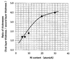
- FIG. 1 is a diagram showing the relationship between the amount of added Ni and the ratio of film thickness when the side etching width is 5.0 ⁇ m in wiring processing of a two-layer laminated film composed of a Cu—Ni—N thin film and a Cu thin film. It is.
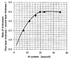
- FIG. 2 is a diagram showing the relationship between the Al addition amount and the film thickness ratio when the side etching width is 5.0 ⁇ m in the wiring processing of the two-layer laminated film composed of the Cu—Al—N thin film and the Cu thin film. It is.
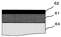
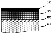
- FIG. 3 is a schematic cross-sectional view showing a structural example of the laminated film of the present invention.
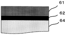
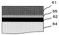
- FIG. 4 is a schematic sectional view showing another structural example of the laminated film of the present invention.
- FIG. 1 is a diagram showing the relationship between the amount of added Ni and the ratio of film thickness when the side etching width is 5.0 ⁇ m in wiring processing of a two-layer laminated film composed of a Cu—Ni—N thin film and
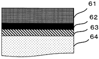
- FIG. 5 is a schematic sectional view showing another structural example of the laminated film of the present invention.
- FIG. 6 is a schematic sectional view showing another structural example of the laminated film of the present invention.
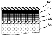
- FIG. 7 is a schematic sectional view showing another structural example of the laminated film of the present invention.
- FIG. 8 is a schematic sectional view showing another structural example of the laminated film of the present invention.
- FIG. 9 is a schematic sectional view showing another structural example of the laminated film of the present invention.
- FIG. 10 is a schematic cross-sectional view showing another structural example of the laminated film of the present invention.
- FIG. 11 is a schematic cross-sectional view showing another structural example of the laminated film of the present invention.
- FIG. 12 is a schematic cross-sectional view showing another structural example of the laminated film of the present invention.
- FIG. 13 is a schematic cross-sectional view schematically showing a configuration of a general liquid crystal display device.
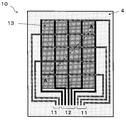
- FIG. 14 is a schematic plan view showing an example of an input device in a capacitive touch panel.
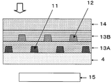
- FIG. 15 is a schematic sectional view showing an example of a sectional structure taken along the dotted line AA in FIG.
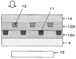
- FIG. 16 is a schematic sectional view showing another example of the sectional structure taken along the dotted line AA in FIG.
- FIG. 17 is a schematic plan view showing another example of the input device in the capacitive touch panel.
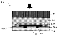
- FIG. 18 is a schematic sectional view showing an example of a sectional structure taken along the dotted line BB in FIG.
- FIG. 19 is a schematic sectional view showing another example of the sectional structure taken along the dotted line BB in FIG.
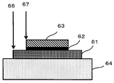
- FIG. 20 is a schematic cross-sectional view illustrating the side etching in the example.
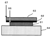
- FIG. 21 is a schematic cross-sectional view illustrating eaves in the example.
- the inventors of the present invention have made extensive studies to solve the above problems.
- the laminated film of the present invention is made of Ag, Al, Cu, or an alloy based on these as the first layer and has an electrical resistivity of 1.0 ⁇ 10 ⁇ 5 ⁇ ⁇ cm or less.
- the present invention further includes an oxide film containing at least one element selected from the group consisting of In, Zn, Sn and Al as the third layer in addition to the first layer and the second layer,
- the visible light reflectance of the three-layer laminated film of the first layer, the second layer, and the third layer is 30% or less, and the sheet resistance of the three-layer laminated film is 1.0 ⁇ / ⁇ or less.
- a laminated film is also included.
- the nitrogen-containing Cu alloy film having a reflectance of 45% or less at a wavelength of 650 nm and a light absorptance of 40% or more at a wavelength of 650 nm when the film thickness is 50 nm Contributes to improved workability.
- the two-layer laminated film and the three-layer laminated film containing the nitrogen-containing Cu alloy film as the second layer exhibit low electrical resistance, improve visibility, and have excellent wiring processability. And found that it can be applied to low reflection wiring.
- the first layer of the present invention is used as a conductive film, for example. Therefore, the first layer can be used as long as it is a metal material having an electric resistivity of 10 ⁇ ⁇ cm or less, and a material made of Ag, Al, Cu, or an alloy based on these can be used. . Among these, it is preferable to use either a Cu film or a Cu alloy film which is low in resistance and inexpensive.
- the electrical resistivity of the first layer is preferably 5.0 ⁇ ⁇ cm or less.
- the electrical resistivity of the first layer is as follows: electrical resistivity of the second layer serving as a light absorption layer: about 1 m ⁇ ⁇ cm, electrical resistivity of the third layer serving as an optical adjustment layer: about several hundreds Since it is smaller than ⁇ ⁇ cm, the current mainly passes through the first layer. Therefore, the sheet resistance of the laminated film itself is a value close to the electrical resistivity of the first layer that is the conductive film.
- the first layer is preferably a Cu alloy film containing at least one Z element selected from the group consisting of Mn, Ni, Co, Ge, Zn and Ti. By including the Z element, adhesion between the first layer and the substrate or another layer can be enhanced. Examples of the Cu alloy film in the first layer include those containing the Z element with the balance being Cu and inevitable impurities.
- the film thickness of the first layer is preferably 40 nm or more in order to achieve a sheet resistance value of the laminated film: 1.0 ⁇ / ⁇ or less.
- the film thickness of the first layer is more preferably 70 nm or more.
- the thickness of the first layer is preferably 400 nm or less, more preferably 300 nm or less.
- the second layer is stacked on the first layer, which is a conductive layer, to absorb incident light and to serve as a light absorption layer that suppresses reflected light.
- the second layer serving as a light absorbing layer As the second layer serving as a light absorbing layer like this, in the present invention, (I) Cu film having a reflectance of 45 nm or less at a wavelength of 650 nm at a film thickness of 50 nm and having a light absorption rate of 40% or more at a wavelength of 650 nm, or a partially nitrided Cu film; or (ii) a film thickness of 50 nm
- a Cu alloy film having a part of the nitrided film, which will be described in detail below, has a reflectance of 45% or less at a wavelength of 650 nm and a light absorption of 40% or more at a wavelength of 650 nm.
- the film (i) may be referred to as a “nitrogen-containing Cu film” or a “CuN film”.
- the “part of the film is nitrided” means that at least nitrogen is contained in the Cu film or the Cu alloy film described later, and it is not necessarily limited to only the nitride of Cu having a stoichiometric composition. There is no need to be configured. That is, when the Cu nitride is expressed as Cu—Ny, for example, y may be 0.1 at%.
- the nitrogen concentration in the second layer may be constant in the second layer or may have a concentration distribution.
- the second layer basically serves only as an optical adjustment of the laminated structure, and as long as it has a prescribed reflectance and light absorption rate, the nitrogen content in the second layer and its Distribution is not a problem.
- the second layer has a reflectance of 45% at a wavelength of 650 nm in the case of a film thickness of 50 nm so as to serve as a light absorption layer as described above.
- the light absorptance at a wavelength of 650 nm needs to satisfy 40% or more.
- the reflectance is preferably 40% or less, more preferably 35% or less.
- the light absorption rate is preferably 45% or more.
- the laminated film of the present invention when used as a low reflection wiring, it is also required to have excellent wiring workability.
- the wiring processability of the laminated film is mainly determined by the etching rate difference between the first layer and the second layer.
- the second layer has a higher etching rate than the first layer, and is evaluated in the examples described later.
- Side etching width or eaves width tends to increase. Therefore, in order to obtain a good wiring shape, the etching rates of the first layer and the second layer need to be close to each other.
- the inventors of the present invention have intensively studied to obtain a film having low electrical resistance, low reflection, and good wiring workability. As a result, excellent wiring processability can be easily obtained if the film contains at least one X element selected from Ni and Al, the remainder being Cu and inevitable impurities, and a part of the film is nitrided. I found.
- this partially nitrided Cu alloy film may be referred to as “nitrogen-containing Cu alloy film” or “Cu—XN film”.
- X of the “Cu—X—N film” is one or more of Ni and Al.
- the etching rate can be made slower than the case where the X element is not included, and as a result, the wiring processability can be improved.
- These elements may be used alone or in combination of two kinds.
- a nitrogen component containing Ni as an X element and the balance being Cu and inevitable impurities or a nitrogen containing Cu alloy film in which the metal component contains Al as an X element and the balance being Cu and inevitable impurities An alloy film is mentioned.
- Ni and Al are preferable to contain both Ni and Al as the X element.
- a nitrogen-containing Cu alloy film in which the metal component contains both Ni and Al as the X element and the balance is Cu and inevitable impurities is preferably used.
- the preferable content of the X element is preferably 5 atomic% or more, more preferably 10 atomic% or more, and further preferably 20 atomic% or more. Even if Ni is contained excessively, the effect of improving the wiring workability is saturated. On the other hand, since Ni is expensive, when there is much content, it will lead to the increase in material cost. Further, since Ni is an element having magnetism, when the content is large, there is a problem that DC discharge becomes difficult and the process time increases in the sputtering method optimal as the method for forming this nitrogen-containing Cu alloy film. Therefore, the upper limit of the Ni content is preferably 70 atomic percent or less, and more preferably 50 atomic percent or less.
- the Al content is preferably 3 atomic% or more, more preferably 4.5 atomic% or more, further preferably 7 atomic% or more, particularly preferably 15 It is at least atomic percent.
- the upper limit can be set to 40 atomic%.
- the film thickness of the second layer can be, for example, in the range of 10 nm to 300 nm in both cases (i) and (ii).
- the visible light reflectance of the two-layer laminated film of the first layer and the second layer is 45% or less, and the sheet resistance of the two-layer laminated film is 1. 0 ⁇ / ⁇ or less.
- the laminated film is useful as a low reflective conductive film.
- the wiring workability can be improved by controlling the ratio between the thickness of the first layer and the thickness of the second layer.
- the first layer thickness / second layer thickness is preferably 1.4 or less.
- a more preferable first layer thickness / second layer thickness is 1.0 or less.
- the etching rate is slowed by the addition of an alloy element such as Ni or Al, thereby improving the wiring workability.
- it is effective to control the laminated structure, specifically, the ratio of the film thickness of the first layer and the film thickness of the second layer, as described below, in order to ensure excellent wiring processability.
- FIG. 1 shows the amount of Ni and the ratio of the film thickness of the first layer and the film thickness of the second layer when the absolute value of the side etching width is 5.0 ⁇ m when the wiring is processed by the method of the embodiment described later. That is, the relationship between the first layer thickness / second layer thickness is shown by plots and approximate curves.
- the Ni amount is shown as the Ni addition amount.
- the area below the approximate curve is an area where the absolute value of the side etching width is less than 5.0 ⁇ m, and the area above the approximate curve is an absolute value of the side etching width of more than 5.0 ⁇ m. It is an area.
- FIG. 2 shows the amount of Al and the ratio of the thickness of the first layer to the thickness of the second layer when the side etching width becomes 5.0 ⁇ m when the wiring is processed, that is, the thickness of the first layer / the first layer.
- the relationship with the two-layer film thickness is shown by plots and approximate curves.
- the Al amount is shown as the Al addition amount.
- the region below the approximate curve is a region where the side etching width is less than 5 ⁇ m
- the region above the approximate curve is a region where the side etching width is greater than 5 ⁇ m.
- the first layer thickness / The two-layer film thickness needs to be 1.0 or less. If the film thickness of the first layer is reduced to satisfy this ratio, the conductivity of the laminated film tends to decrease. On the other hand, if the film thickness of the second layer is increased, the film formation time increases and the process cost increases. Tend to. For these reasons, the amount of Al is preferably 3 atomic% or more as described above.
- the third layer of the present invention is used as an optical adjustment layer, for example, and contributes to the realization of a low reflectance together with the second layer described above.
- This third layer is an oxide film containing at least one element selected from the group consisting of In, Zn, Sn, and Al.
- An oxide film containing at least In is preferable.
- ITO As In—Sn—O, IZO as In—Zn—O, ZnO, ZTO as Zn—Sn—O, ZAO as Zn—Al—O, or the like is preferably used.
- the film thickness of the third layer can be in the range of 10 nm to 300 nm, for example.
- the laminated film of the present invention essentially includes the first layer and the second layer, and further includes the third layer as necessary.
- the laminated film of the present invention may further have other layers.
- a film made of general Mo, Ni, Ti, Cr or an alloy based on these, preferably a Mo film may be formed as the adhesion layer.
- a Mo film can be formed on at least one surface of the second layer.
- the thickness of the adhesion layer can be set to, for example, 5 to 30 nm.
- the three-layer laminated film of the present invention including the first layer, the second layer, and the third layer has a visible light reflectance of 30% of the three-layer laminated film including the first layer, the second layer, and the third layer.
- the sheet resistance of the three-layer laminated film is 1.0 ⁇ / ⁇ or less. This three-layer-containing laminated film is useful as a low reflection conductive film or a low reflection wiring.
- FIG. 3 is a schematic sectional view showing a structural example of the laminated film of the present invention.
- a first layer 61 and a second layer 62 are sequentially laminated on a substrate 64 which is a transparent substrate.
- the said transparent substrate is normally used for the technical field of this invention, and will not be specifically limited if it has transparency, A glass substrate and a resin substrate can be used.
- the transparent substrate may be simply referred to as “substrate”.
- FIG. 4 is a diagram showing another structural example of the laminated film of the present invention.
- a structure pattern opposite to that in FIG. 3, that is, a structure in which the second layer 62 and the first layer 61 are sequentially laminated on the substrate 64 may be used.
- the position of the second layer 62 provided as the light absorption layer is for the purpose of controlling the reflection of the first layer 61 which is a metal thin film. Therefore, the second layer 62 is formed on the light incident side of the first layer 61. That's fine.
- an adhesion layer 65 may be formed on at least one surface of the first layer 61.
- the material of the adhesion layer 65 include a film made of Mo, Ni, Ti, Cr, or an alloy based on these, and preferably a Mo film.
- an adhesion layer 65 can be provided between the substrate 64 and the first layer 61 or between the first layer 61 and the second layer 62.
- FIG. 8 is a schematic sectional view showing another structural example of the laminated film of the present invention.
- a structure in which a first layer 61, a second layer 62, and a third layer 63 are sequentially stacked on a substrate 64 may be employed.
- FIG. 9 is a schematic sectional view showing another structural example of the laminated film of the present invention.
- a structure pattern opposite to that shown in FIG. 8, that is, a structure in which a third layer 63, a second layer 62, and a first layer 61 are sequentially stacked on a substrate 64 may be used.
- the position of the second layer 62 provided as the light absorption layer is for the purpose of controlling the reflection of the first layer 61 which is a metal thin film. Therefore, the second layer 62 is formed on the light incident side of the first layer 61. That's fine.
- FIG. 10 to FIG. 12 are diagrams showing other structural examples of the laminated film of the present invention.
- an adhesion layer 65 may be formed on at least one surface of the first layer 61.
- an adhesion layer 65 can be provided between the substrate 64 and the first layer 61 or between the first layer 61 and the second layer 62.
- the three-layer-containing laminated film of the present invention has a visible light reflectance of 30% or less and a sheet resistance of the laminated film of 1.0 ⁇ / ⁇ or less. In order to ensure the characteristics, for example, it is recommended to control the film thickness of the first layer as described above.
- the nitrogen-containing Cu alloy film or laminated film of the present invention is useful as a low reflection conductive film or low reflection wiring. Moreover, the nitrogen-containing Cu alloy film and laminated film of the present invention can be applied to an electromagnetic wave shield as well as a display device and an input device including a touch panel sensor. Below, the specific structure in the case of utilizing the laminated film of this invention for the wiring electrode of a touch panel, for example is demonstrated.
- liquid crystal display device part in the touch panel structure will be described.
- the present invention will be described using a liquid crystal display device as an example of the display device.
- the present invention is not limited to this, and can be applied to other display devices such as an organic EL display device.
- FIG. 13 is a schematic cross-sectional view schematically showing a configuration of a general liquid crystal display device.
- a liquid crystal display device 1 shown in FIG. 13 includes a thin film transistor (hereinafter referred to as TFT) substrate 2.
- the TFT substrate 2 is, for example, a TFT array substrate.
- a counter substrate 3 is disposed opposite to the TFT substrate 2. In FIG. 13, a thick arrow indicates the viewing direction.
- the counter substrate 3 is, for example, a color filter (CF, Color Filter) substrate 4 and is disposed on the side to be visually recognized.
- CF color filter
- BM black matrix
- BM black matrix
- a liquid crystal layer 7 into which liquid crystal is introduced is sandwiched between the TFT substrate 2 and the counter substrate 3, and the liquid crystal layer 7 is sealed with a liquid crystal sealing material 8. Furthermore, although not shown, a polarizing plate and a retardation plate are provided on the outer surface of the counter substrate 3. Further, although not shown, a backlight unit or the like is disposed on the non-viewing side of the liquid crystal display panel, that is, below the TFT substrate 2 in FIG.
- the input device including the electrode of the present invention is disposed above the color filter substrate 4 of the liquid crystal display device 1, that is, on the operation surface side.
- an electrode that can use the laminated film of the present invention from a transparent conductive film or the like, it may be referred to as a “metal electrode”.
- FIG. 14 is a schematic plan view showing an example of an input device in a capacitive touch panel.
- the wiring has a lattice shape. More specifically, a plurality of driving metal electrodes arranged in the X direction for each row, that is, the driving electrodes 11 are arranged on the color filter substrate 4 which is a kind of transparent substrate; and arranged in the Y direction for each column. And a plurality of metal electrodes for detection, that is, detection electrodes 12 are provided.
- the drive electrode 11 and the detection electrode 12 are provided in different layers, and are insulated from each other by the insulating layer 13.
- a voltage is applied to the electrodes, and when the user touches the surface of the input device, the capacitance between the drive electrode 11 and the detection electrode 12 changes to generate a current. . By detecting this current with the drive electrode 11 and the detection electrode 12, the touch position of the user is detected.
- This configuration uses a metal electrode having a low resistance as the driving electrode 11 and the detection electrode 12, so that each electrode can be formed as a narrow wiring. Therefore, it has a feature that the transmittance of the active area can be sufficiently increased.
- the driving electrode 11 and the detection electrode 12 can be configured with narrow wiring, and high detection sensitivity and light transmittance can be secured at the same time.
- FIG. 15 and FIG. 16 show examples of the sectional structure taken along the dotted line AA in FIG. 15 and 16 are schematic sectional views showing an example of a structure in which the input device 10 of FIG. 14 is mounted on the color filter substrate 4 of the liquid crystal display device 1 shown in FIG.
- a thick arrow indicates the direction of incident external light.
- a plurality of first metal electrodes 11 arranged in the X direction for each row are arranged on the same layer on the color filter substrate 4. Further, a plurality of second metal electrodes 12 arranged in the Y direction for each column are arranged in a different layer from the first metal electrode 11.
- the plurality of first metal electrodes 11 and second metal electrodes 12 are preferably arranged immediately above the black matrix, although not shown, in order not to deteriorate the visibility of the display device.
- the first insulating layer 13A Between the plurality of first metal electrodes 11, between the plurality of second metal electrodes 12, and between the first metal electrode 11 and the second metal electrode 12, the first insulating layer 13A, A second insulating layer 13B is disposed.
- first insulating layer 13A and the second insulating layer 13B for example, a known translucent insulating resin can be used. And the cover glass 14 is provided so that the surface in which the 2nd insulating layer 13B was provided may be covered.
- reference numeral 15 denotes a backlight.
- a metal electrode having excellent conductivity and low reflectivity is proposed. it can.
- FIG. 17 is a schematic plan view showing another example of the input device in the capacitive touch panel.
- the electrode is a diamond-shaped transparent electrode.
- the transparent substrate 33, a plurality of first electrode patterns 31A having a diamond shape arranged in the X direction for each row, and the first transparent electrode 31A are connected to the upper portion of the transparent substrate 33.
- One bridge electrode 31B, a plurality of second electrode patterns 32A having a diamond shape arranged in the Y direction for each column, and a second bridge electrode 32B for connecting the second transparent electrodes 32A are provided.
- the first transparent electrode composed of the first electrode pattern 31A and the bridge electrode 31B and the second transparent electrode composed of the second electrode pattern 32A and the bridge electrode 32B are insulated from each other by an insulating layer (not shown).
- Each electrode pattern is connected to a control unit (not shown) via the outer peripheral wiring 31C or 32C.
- a transparent conductive material is generally used for the first electrode pattern 31A and the second electrode pattern 32A.
- a metal oxide such as ITO that is In—Sn—O or IZO that is In—Zn—O can be given.
- An input device with high detection sensitivity is produced by using the laminated film of the present invention for the bridge electrodes 31B and 32B that connect the electrode patterns of the touch panel with this configuration and the outer peripheral wirings 31C and 32C of the input device. Can do.
- This configuration can be applied to an external input device type in which a cover glass, a touch panel, and a liquid crystal cell are individually manufactured and bonded, that is, an out-cell structure type liquid crystal display device.
- the out-cell structure has a simple manufacturing method and is widely used in liquid crystal display devices.
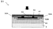
- FIGS. 18 and 19 Examples of the cross-sectional structure taken along the dotted line BB in FIG. 17 are shown in FIGS.
- the thick arrows in FIGS. 18 and 19 indicate the viewing direction.
- a first transparent electrode 52A arranged in parallel to the X direction and a parallel to the Y direction are arranged on the color filter substrate 4 which is the first transparent substrate.
- a second transparent electrode 53 is provided on the color filter substrate 4 which is the first transparent substrate.
- the first transparent electrodes 52A, the second transparent electrodes 53, and the first transparent electrodes 52A and the second transparent electrodes 53 are separated from each other by the insulating layer 54 so that they do not contact each other.
- metal electrodes are provided as the transparent electrodes 52A and 53, the insulating layer 54, and the first bridge electrode 52B on the second transparent substrate, that is, the back surface side of the cover glass 41. This is different from FIG.
- the user's touch position is detected by detecting a current generated by a change in capacitance.
- the first bridge electrode 52B electrically connects the first transparent electrodes 52A.
- the adhesive layer 44 in FIGS. 18 and 19 is a layer that joins the cover glass 41, the color filter substrate 4, and the respective transparent electrodes, bridge electrodes, and the like.
- the adhesive layer is a transparent adhesive layer such as OCA (Optically Clear Adhesive, transparent adhesive sheet) or OCR (Optically Clear Resin, optical transparent resin), and an acrylic adhesive is used.
- the laminated film of the present invention can be suitably used as the first bridge electrode 52B in FIG. 18 or FIG.
- the bridge electrode 52B includes the two-layer-containing laminated film of any of FIGS. 3 to 7 including the second layer 62 and the first layer 61, or the third layer 63, the second layer 62, and the first layer 61.
- a metal electrode having excellent conductivity and low reflectance can be proposed.
- the laminated film of the present invention has a low sheet resistance and a low reflectance. Therefore, it can be applied not only to the electrodes used in the input region of the input device but also to the wiring on the outer periphery of the panel by extending the electrodes, and there is an advantage that the manufacturing process can be simplified.
- the two-layer-containing laminated film having the first layer and the second layer or the three-layer-containing laminated film having the first layer, the second layer, and the third layer is processed by wiring, and used as a metal electrode.
- the input device including the above is applied to a so-called on-cell structure formed between a liquid crystal color filter and a cover glass
- the present invention is not limited to this.
- a so-called out-cell structure in which an input device in which the sensor electrode of the touch panel is formed of a transparent conductive film and the bridge wiring between the transparent conductive films is formed of a metal electrode is formed separately from the liquid crystal cell.
- the present invention is not limited to this.
- the laminated film of the present invention can be applied to a so-called in-cell structure, for example, in a liquid crystal display device, for example, a liquid crystal display device in which an electrode of an input device is incorporated between a TFT substrate and a color filter substrate.
- a liquid crystal display device for example, a liquid crystal display device in which an electrode of an input device is incorporated between a TFT substrate and a color filter substrate.
- the input device to which the electrode using the laminated film of the present invention is applied includes an input device having an input means in a display device such as a touch panel or an input device having no display device such as a touch pad. Both are included. Specifically, an input device for operating the device by combining the above various display devices and position input means and pressing a display on the screen, or a display device separately installed corresponding to the input position on the position input means
- the laminated film of the present invention can also be used for an electrode of an input device for operation.
- sputtering is performed because of thinning, uniformity of alloy components in the film, easy control of the amount of added elements, high throughput during production, etc. It is preferable to form a film by a sputtering method using a target.
- the second layer in the laminated film of the present invention that is, the nitrogen-containing Cu film or the nitrogen-containing Cu alloy film
- a pure Cu sputtering target or a Cu alloy sputtering target having a desired alloy composition The method of forming by reactive sputtering method in the atmosphere containing nitrogen gas or nitrogen-containing gas is mentioned.
- two or more pure metal targets or alloy targets having different compositions may be used in place of the alloy sputtering target, and these may be discharged simultaneously to form the second layer.
- the sputtering target itself may be a material containing a Cu nitrogen compound or a Cu alloy nitrogen compound.
- the conditions of the reactive sputtering method for forming the second layer may be appropriately controlled according to the film thickness, film quality, and nitrogen concentration to be introduced. For example, in order to obtain a second layer satisfying a prescribed visible light reflectance or light absorption rate, it is possible to control the gas pressure during film formation.
- the shape of the sputtering target is not particularly limited, and an arbitrary shape such as a square plate shape, a circular plate shape, a donut plate shape, or a cylindrical shape can be used according to the shape or structure of the sputtering apparatus.
- the method for producing a nitrogen-containing Cu alloy film or laminated film of the present invention is particularly characterized by the film formation conditions for the second layer.
- a method for forming each layer other than the second layer that is, the first layer, the third layer, and other layers such as an adhesion layer included as necessary, a method usually used in the technical field of the present invention is appropriately adopted. Can do.
- a non-alkali glass plate having a thickness of 0.7 mm and a diameter of 4 inches was prepared, and the layers shown in Tables 1 to 5 were formed on the non-alkali glass plate by DC magnetron sputtering.
- a film was formed.
- Table 1 a sample was prepared in which a pure metal film or alloy film shown as the first layer in Tables 2 to 5 was formed on the alkali glass plate.
- Tables 2 and 3 a Cu film, an Al film or an Ag film is formed as the first layer on the alkali glass plate, and a CuN film or a Cu—X—N film shown in Table 2 or Table 3 is formed as the second layer in this order.
- a sample in which an IZO film, that is, an In—Zn—O film was formed as the second layer was also prepared as a comparative example.
- Tables 4 and 5 on the alkali glass plate, the Cu film, Cu alloy film, Al film or Ag film shown in Table 4 or Table 5 as the first layer, and the CuN film shown in Table 4 or Table 5 as the second layer.
- a sample was prepared in which a Cu—X—N film and an oxide film shown in Table 4 or 5 were formed as the third layer.
- IZO is In—Zn—O
- ITO is In—Sn—O
- ZTO is Zn—Sn—O
- ZAO Zn—Al—O.
- a sample was prepared in which the second layer CuN film or Cu—X—N film shown in Tables 2 to 5 was formed to a thickness of 50 nm on the alkali glass plate.
- the atmosphere in the chamber was once adjusted to an ultimate vacuum of 3 ⁇ 10 ⁇ 6 Torr before film formation, and then each layer was formed as shown below using a disk-type sputtering target having a diameter of 4 inches. A sample was obtained by sputtering.
- the film formation of the first layer was performed under the following conditions using a pure metal or alloy sputtering target having the same component composition as each of the first layers shown in Tables 1 to 5.
- Sputtering conditions Film forming method: Sputtering method Film forming apparatus: CS-200 manufactured by ULVAC Substrate temperature: room temperature Deposition gas: Ar gas Gas pressure: 2 mTorr Sputtering power: 10W to 500W Degree of vacuum: 1 ⁇ 10 -6 Torr or less
- Second Layer When a CuN film was formed as the second layer, a CuN film was formed by a reactive sputtering method using a pure Cu target and a mixed gas of Ar gas and N 2 gas. In the case where a Cu—X—N film was formed as the second layer, a plurality of sputtering targets containing an X element were used, the film formation power was adjusted so as to have a desired composition, and the film was formed by co-sputtering. In either case, the sputtering conditions are as follows.
- Film forming method Sputtering method
- Film forming apparatus CS-200 manufactured by ULVAC Substrate temperature: room temperature
- Deposition gas Ar gas and N 2 gas mixture gas pressure: 1 mTorr to 5 mTorr
- Sputter power 500 W in the case of film formation using one target having a desired composition.
- each target was set to an arbitrary power so as to have a desired composition.
- Degree of vacuum 1 ⁇ 10 -6 Torr or less
- the third layer is formed by a reactive sputtering method using an oxide target having the same component composition as the oxide film shown in Table 4 or Table 5, and using a mixed gas of Ar gas and O 2 gas. Filmed. Details of the oxide target and sputtering conditions are shown below.
- the electric resistivity of Cu film, Cu alloy film, Al film and Ag film used as the first layer of the laminated film in the present invention is as follows. Measured as follows. That is, the electrical resistivity was measured by a four-terminal method using a sample in which only the first layer was formed on the substrate by the above method. In this example, a material having an electric resistivity of 1.0 ⁇ 10 ⁇ 5 ⁇ ⁇ cm or less is accepted as a material suitable for the first layer, and the electric resistivity is 1.0 ⁇ 10 ⁇ 5 ⁇ ⁇ cm. Exceeded was rejected. The results are shown in Table 1. In Table 1, for example, No. “3.0E-06” of 1 means 3.0 ⁇ 10 ⁇ 6 . The same applies to the electrical resistivity shown in Tables 2 to 5 below.
- the electrical resistivity of the Cu film, Cu alloy film, Al film, and Ag film used as the first layer in this example was 1.0 ⁇ 10 ⁇ 5 ⁇ ⁇ cm or less.
- the reflectance and light absorption rate were measured with a spectrophotometer: V-570 manufactured by JASCO Corporation using a sample in which a CuN film or Cu—XN film formed as the second layer was formed to a thickness of 50 nm.
- V-570 manufactured by JASCO Corporation
- a reflectance at a wavelength of 650 nm of 45% or less and a light absorption at a wavelength of 650 nm of 40% or more was suitable as a light absorption layer.
- the visible light reflectance and sheet resistance of the two-layer laminated film of the first layer and the second layer, or the visible light reflection of the three-layer laminated film of the first layer, the second layer, and the third layer are used.
- Rate and sheet resistance were measured, but not limited to the above laminated structure, between the substrate and the first layer, between the first layer and the second layer, or between the second layer and the third layer, such as an adhesion layer Even when other layers are included, it has been separately confirmed that the visible light reflectance and sheet resistance satisfy the above acceptance criteria.
- the wiring workability of the laminated film was evaluated as follows. That is, using the sample of the above-mentioned two-layer laminated film or three-layer laminated film, wet etching processing was performed using an etching solution obtained by diluting Pure etch F108 made of Hayashi Pure Chemical Industries, Ltd. containing iron chloride 10 times with pure water. .
- the cross-sectional shape and planar shape of the sample subjected to the etching process were observed using an electron microscope S-4000 manufactured by Hitachi Power Solutions. Then, in the cross-sectional observation image, as schematically shown in FIG. 20, the one having the first layer end 66 longer than the second layer end 67 was determined as “side etching”. Further, as schematically shown in FIG. 21, a case where the first layer end 66 is shorter than the second layer end 67 is determined to be “eave”. Then, from the plane observation image, the side etching width and the eave width were measured, and the side etching width was determined as a negative number, and the eave width was determined as a positive number. The results are shown in the “wiring processability” column of Tables 2-5.
- the absolute value of the side etching width or the eave width is 5.0 ⁇ m or less, and it is shown as “A” in Tables 2 to 5 because it is excellent in the wiring processability of the laminated film and is passed. It was. On the other hand, in the cases where the absolute value is more than 5.0 ⁇ m, the wiring processability of the laminated film is inferior and is rejected.
- Tables 2 and 3 show the characteristics of the first layer and the two-layer laminated film in which the second layer is formed on the light incident side of the first layer.
- No. 1 is an example in which an IZO film having a reflectance of 45% or less as a second layer but having an absorptivity at a wavelength of 650 nm significantly lower than 40% is laminated.
- the visible light reflectance of the laminated film including this IZO film was also increased. In this way, No.
- the laminated film 1 does not have sufficient spectral characteristics and is not suitable as a low reflection conductive film or low reflection wiring.
- Nos. 3 to 7 are examples in which a CuN film having a reflectance of 45% or less and an absorptance of 40% or more is laminated as the second layer. In this way, the No. including the second layer having sufficient spectral characteristics.
- Each of the laminated films 3 to 7 has a low visible light reflectance and a low sheet resistance, and is suitable as a low reflection conductive film.
- No. 2 and No. No. 4 has the same film thickness as the component of the second layer and different optical characteristics because the gas pressure at the time of forming the second layer is different between the two.
- the first layer thickness / second layer thickness is preferably 1.4 or less, and more preferably 1.0 or less.
- Examples 8 to 16 are examples in which a Cu—Ni—N film having a reflectance of 45% or less and an absorptance of 40% or more is laminated as the second layer. In this way, the No. including the second layer having sufficient spectral characteristics. Any of the laminated films 8 to 16 has low visible light reflectance and low sheet resistance, and is suitable as a low reflective conductive film.
- the first layer thickness / second layer thickness or component composition is controlled. It turns out that it is good to do. That is, from the comparison with FIG. 1 described above, in order to ensure excellent wiring processability, the first layer thickness / second layer thickness is 1.4 or less when the Ni amount is 5.0 atomic%. When the Ni content is 7.0 atomic%, it is 1.4 or less, when the Ni content is 10.0 atomic%, it is 1.8 or less, and when the Ni content is 20.0 atomic%, it is 3 .6 or less is good. In addition, from the viewpoint of expanding the allowable film thickness range of the first layer and the second layer, the amount of Ni is preferably 5 atomic% or more, and more preferably 10 atomic% or more.
- Reference numerals 17 to 25 are examples in which a Cu—Al—N film having a reflectance of 45% or less and an absorption of 40% or more is laminated as the second layer. In this way, the No. including the second layer having sufficient spectral characteristics.
- the laminated films 17 to 25 all have low visible light reflectance and low sheet resistance, and are suitable as low reflection conductive films.
- the first layer thickness / second layer thickness or the composition of the components is controlled. It turns out that is good. That is, from the comparison with FIG. 2 described above, in order to ensure excellent wiring processability, the first layer thickness / second layer thickness is 2.0 or less when the Al amount is 7.2 atomic%. It can be seen that, when the Al content is 11.7 atomic%, it is preferably 3.0 or less, and when the Al content is 16.4 atomic%, it is preferable to set it to 3.6 or less.
- the Al content is preferably 3 atomic% or more, more preferably 7 atomic% or more, and further preferably 15 atomic% or more.
- No. in Table 3 Nos. 26 to 34 are examples in which a Cu—Ni—Al—N film having a reflectance of 45% or less and an absorptance of 40% or more is laminated as the second layer. In this way, the No. including the second layer having sufficient spectral characteristics.
- the laminated films 26 to 34 all have low visible light reflectance and low sheet resistance, and are suitable as low reflection conductive films. No.
- the laminated films 26 to 34 have excellent wiring processability and are useful as low reflection wiring. As described above, it is considered that the inclusion of both Ni and Al slows the etching rate and improves the wiring workability.
- Reference numerals 35 and 36 show examples in which an Al film or an Ag film is used for the first layer. If the second layer is a film defined by the present invention, it can be seen that even if an Al film or an Ag film is used for the first layer, the obtained laminated film satisfies the characteristics required for a low reflective conductive film.
- Tables 4 and 5 show the characteristics of the first layer and the three-layer laminated film in which the second layer and the third layer are sequentially formed on the light incident side of the first layer.
- No. in Table 4 1 is an example in which a CuN film having a reflectivity at a wavelength of 650 nm of more than 45% and an absorptivity at a wavelength of 650 nm of less than 40% is stacked as the second layer.
- No. in Table 4 Nos. 2 to 7 are examples in which a CuN film having a reflectance of 45% or less and an absorption rate of 40% or more is laminated as the second layer. In this way, the No. including the second layer having sufficient spectral characteristics. Any of the laminated films 2 to 6 has low visible light reflectance and low sheet resistance, and is suitable as a low reflective conductive film. No. No. 7 had a high sheet resistance because the first layer was thin. In order to sufficiently reduce the sheet resistance of the laminated film, the film thickness of the first layer is, for example, 70 nm or more.
- the first layer thickness / second layer thickness is preferably 1.3 or less, and more preferably 1.0 or less.
- Examples 8 to 16 are examples in which a Cu—Ni—N film having a reflectance of 45% or less and an absorptance of 40% or more is laminated as the second layer. In this way, the No. including the second layer having sufficient spectral characteristics. Any of the laminated films 8 to 16 has low visible light reflectance and low sheet resistance, and is suitable as a low reflective conductive film.
- the first layer thickness / second layer thickness or component composition is controlled. It turns out that it is good to do. That is, from the above comparison, in order to ensure excellent wiring processability, the first layer thickness / second layer thickness should be 1.2 or less when the Ni content is 5.0 atomic%. When the Ni content is 7.0 atomic%, it is 1.6 or less, when the Ni content is 10.0 atomic%, it is 2.0 or less, and when the Ni content is 20.0 atomic%, it is 3.6 or less. You can see that it is good.
- the amount of Ni is preferably 5 atomic% or more, and more preferably 10 atomic% or more.
- Reference numerals 17 to 25 are examples in which a Cu—Al—N film having a reflectance of 45% or less and an absorption of 40% or more is laminated as the second layer. In this way, the No. including the second layer having sufficient spectral characteristics.
- the laminated films 17 to 25 all have low visible light reflectance and low sheet resistance, and are suitable as low reflection conductive films.
- the first layer thickness / second layer thickness or the composition of the components is controlled. It turns out that is good. That is, from the above comparison, in order to ensure excellent wiring processability, the first layer thickness / second layer thickness should be about 1.8 or less when the Al content is 7.2 atomic%. It is well understood that when the Al content is 11.7 atomic%, it is good to set it to 2.8 or less, and when the Al content is 16.4 atomic%, it should be 3.6 or less.
- the Al content is preferably 7 atomic% or more, and more preferably 15 atomic% or more.
- No. in Table 5 Nos. 26 to 34 are examples in which a Cu—Ni—Al—N film having a reflectance of 45% or less and an absorptance of 40% or more is laminated as the second layer. In this way, the No. including the second layer having sufficient spectral characteristics.
- the laminated films 26 to 34 all have low visible light reflectance and low sheet resistance, and are suitable as low reflection conductive films. No.
- the laminated films 26 to 34 have excellent wiring processability and are useful as low reflection wiring. As described above, it is considered that the inclusion of both Ni and Al slows the etching rate and improves the wiring workability.
- No. in Table 5 35 to 46 show examples in which various Cu alloy films are used for the first layer.
- the excellent optical characteristics required for the laminated film are low even if a Cu alloy film having any alloy composition shown in Table 5 is used as the first layer. It can be seen that the sheet resistance and excellent wiring processability are all satisfied.
- Table 5 47 and 48 show examples in which an Al film or an Ag film is used for the first layer. If the second layer is a film defined by the present invention, it can be seen that even if an Al film or an Ag film is used for the first layer, the obtained laminated film satisfies the characteristics required for a low reflective conductive film.
- Reference numerals 49 to 52 are examples in which the third layer acting as the optical adjustment layer is an ITO film, a ZnO film, a ZTO film, or a ZAO film. This No. From the results of 49 to 52, even when any of the above oxide films is laminated, all of the excellent optical characteristics, low sheet resistance and excellent wiring processability required for the laminated film are satisfied. I understand.
Landscapes
- Chemical & Material Sciences (AREA)
- Chemical Kinetics & Catalysis (AREA)
- Engineering & Computer Science (AREA)
- Materials Engineering (AREA)
- Mechanical Engineering (AREA)
- Metallurgy (AREA)
- Organic Chemistry (AREA)
- Laminated Bodies (AREA)
- Physical Vapour Deposition (AREA)
- Conductive Materials (AREA)
- Non-Insulated Conductors (AREA)
Applications Claiming Priority (2)
| Application Number | Priority Date | Filing Date | Title |
|---|---|---|---|
| JP2015069999A JP2016191967A (ja) | 2015-03-30 | 2015-03-30 | 窒素含有Cu合金膜、積層膜、およびこれらの製造方法、ならびにCu合金スパッタリングターゲット |
| JP2015-069999 | 2015-03-30 |
Publications (1)
| Publication Number | Publication Date |
|---|---|
| WO2016158181A1 true WO2016158181A1 (ja) | 2016-10-06 |
Family
ID=57005605
Family Applications (1)
| Application Number | Title | Priority Date | Filing Date |
|---|---|---|---|
| PCT/JP2016/056491 WO2016158181A1 (ja) | 2015-03-30 | 2016-03-02 | 窒素含有Cu合金膜、積層膜、およびこれらの製造方法、ならびにCu合金スパッタリングターゲット |
Country Status (3)
| Country | Link |
|---|---|
| JP (1) | JP2016191967A (zh) |
| TW (1) | TW201641699A (zh) |
| WO (1) | WO2016158181A1 (zh) |
Cited By (3)
| Publication number | Priority date | Publication date | Assignee | Title |
|---|---|---|---|---|
| CN109504942A (zh) * | 2019-01-18 | 2019-03-22 | 黄饶 | 一种金属膜层表面超低反射率的加工工艺 |
| CN113481467A (zh) * | 2021-06-01 | 2021-10-08 | 北京科技大学 | 抑制Al-Ni纳米多层膜相变过程有序金属间化合物生成的方法 |
| CN114309586A (zh) * | 2021-12-31 | 2022-04-12 | 西安稀有金属材料研究院有限公司 | 一种高熵合金/炭黑复合电磁吸波材料及其制备方法 |
Families Citing this family (1)
| Publication number | Priority date | Publication date | Assignee | Title |
|---|---|---|---|---|
| JP7339016B2 (ja) * | 2019-04-24 | 2023-09-05 | 株式会社アルバック | 表示装置、配線膜、配線膜製造方法 |
Citations (3)
| Publication number | Priority date | Publication date | Assignee | Title |
|---|---|---|---|---|
| JP2010206062A (ja) * | 2009-03-05 | 2010-09-16 | Toray Ind Inc | 導電性フィルムおよびディスプレイ用フィルター |
| WO2014035196A1 (ko) * | 2012-08-31 | 2014-03-06 | 주식회사 엘지화학 | 금속 구조체 및 이의 제조방법 |
| KR20150029561A (ko) * | 2013-09-10 | 2015-03-18 | 히타치 긴조쿠 가부시키가이샤 | 적층 배선막 및 그 제조 방법 및 Ni 합금 스퍼터링 타깃재 |
Family Cites Families (2)
| Publication number | Priority date | Publication date | Assignee | Title |
|---|---|---|---|---|
| JP5938290B2 (ja) * | 2012-07-31 | 2016-06-22 | 小川 倉一 | 透明導電膜及びその製造方法 |
| JP2015007263A (ja) * | 2013-06-24 | 2015-01-15 | 株式会社日立ハイテクノロジーズ | 有機デバイス製造装置および有機デバイスの製造方法 |
-
2015
- 2015-03-30 JP JP2015069999A patent/JP2016191967A/ja active Pending
-
2016
- 2016-03-02 WO PCT/JP2016/056491 patent/WO2016158181A1/ja active Application Filing
- 2016-03-17 TW TW105108227A patent/TW201641699A/zh unknown
Patent Citations (3)
| Publication number | Priority date | Publication date | Assignee | Title |
|---|---|---|---|---|
| JP2010206062A (ja) * | 2009-03-05 | 2010-09-16 | Toray Ind Inc | 導電性フィルムおよびディスプレイ用フィルター |
| WO2014035196A1 (ko) * | 2012-08-31 | 2014-03-06 | 주식회사 엘지화학 | 금속 구조체 및 이의 제조방법 |
| KR20150029561A (ko) * | 2013-09-10 | 2015-03-18 | 히타치 긴조쿠 가부시키가이샤 | 적층 배선막 및 그 제조 방법 및 Ni 합금 스퍼터링 타깃재 |
Cited By (5)
| Publication number | Priority date | Publication date | Assignee | Title |
|---|---|---|---|---|
| CN109504942A (zh) * | 2019-01-18 | 2019-03-22 | 黄饶 | 一种金属膜层表面超低反射率的加工工艺 |
| CN113481467A (zh) * | 2021-06-01 | 2021-10-08 | 北京科技大学 | 抑制Al-Ni纳米多层膜相变过程有序金属间化合物生成的方法 |
| CN113481467B (zh) * | 2021-06-01 | 2022-07-22 | 北京科技大学 | 抑制Al-Ni纳米多层膜相变过程有序金属间化合物生成的方法 |
| CN114309586A (zh) * | 2021-12-31 | 2022-04-12 | 西安稀有金属材料研究院有限公司 | 一种高熵合金/炭黑复合电磁吸波材料及其制备方法 |
| CN114309586B (zh) * | 2021-12-31 | 2024-01-26 | 西安稀有金属材料研究院有限公司 | 一种高熵合金/炭黑复合电磁吸波材料及其制备方法 |
Also Published As
| Publication number | Publication date |
|---|---|
| TW201641699A (zh) | 2016-12-01 |
| JP2016191967A (ja) | 2016-11-10 |
Similar Documents
| Publication | Publication Date | Title |
|---|---|---|
| US9845529B2 (en) | Electrode and method for producing same | |
| TWI536403B (zh) | 導電結構體及其製造方法 | |
| JP6021030B2 (ja) | 構造体、タッチパネル及びディスプレイ | |
| WO2017212970A1 (ja) | 積層膜、表示装置及び入力装置 | |
| KR101656581B1 (ko) | 전도성 구조체 및 이의 제조방법 | |
| WO2017016237A1 (en) | Conductive layer in a semiconductor apparatus, display substrate and display apparatus having the same, and fabricating method thereof | |
| KR101987263B1 (ko) | 전도성 구조체 및 이의 제조방법 | |
| CN104838344B (zh) | 触摸面板、触摸面板的制造方法、光学薄膜基板及其制造方法 | |
| WO2016158181A1 (ja) | 窒素含有Cu合金膜、積層膜、およびこれらの製造方法、ならびにCu合金スパッタリングターゲット | |
| KR20160035998A (ko) | 전도성 구조체 및 이의 제조방법 | |
| US20160224151A1 (en) | Electrode to be used in input device and method for producing same | |
| JP6190792B2 (ja) | 電極およびその製造方法 | |
| JP6228530B2 (ja) | 電極およびその製造方法 | |
| JP2019098565A (ja) | 積層体 | |
| JP7326918B2 (ja) | 積層体 | |
| TWI647599B (zh) | 觸控面板、觸控面板之製造方法、顯示裝置及顯示裝置之製造方法 | |
| CN110872687B (zh) | 层叠体及靶材 | |
| JP6157424B2 (ja) | 電極およびその製造方法 | |
| JP2017068219A (ja) | 電極構造 |
Legal Events
| Date | Code | Title | Description |
|---|---|---|---|
| 121 | Ep: the epo has been informed by wipo that ep was designated in this application |
Ref document number: 16772065 Country of ref document: EP Kind code of ref document: A1 |
|
| NENP | Non-entry into the national phase |
Ref country code: DE |
|
| 122 | Ep: pct application non-entry in european phase |
Ref document number: 16772065 Country of ref document: EP Kind code of ref document: A1 |
