WO2016157952A1 - 誘電体材料の製造方法 - Google Patents
誘電体材料の製造方法 Download PDFInfo
- Publication number
- WO2016157952A1 WO2016157952A1 PCT/JP2016/051855 JP2016051855W WO2016157952A1 WO 2016157952 A1 WO2016157952 A1 WO 2016157952A1 JP 2016051855 W JP2016051855 W JP 2016051855W WO 2016157952 A1 WO2016157952 A1 WO 2016157952A1
- Authority
- WO
- WIPO (PCT)
- Prior art keywords
- slurry
- dielectric material
- powder
- organic acid
- metal salt
- Prior art date
- Legal status (The legal status is an assumption and is not a legal conclusion. Google has not performed a legal analysis and makes no representation as to the accuracy of the status listed.)
- Ceased
Links
Images

Classifications
-
- C—CHEMISTRY; METALLURGY
- C04—CEMENTS; CONCRETE; ARTIFICIAL STONE; CERAMICS; REFRACTORIES
- C04B—LIME, MAGNESIA; SLAG; CEMENTS; COMPOSITIONS THEREOF, e.g. MORTARS, CONCRETE OR LIKE BUILDING MATERIALS; ARTIFICIAL STONE; CERAMICS; REFRACTORIES; TREATMENT OF NATURAL STONE
- C04B35/00—Shaped ceramic products characterised by their composition; Ceramics compositions; Processing powders of inorganic compounds preparatory to the manufacturing of ceramic products
- C04B35/01—Shaped ceramic products characterised by their composition; Ceramics compositions; Processing powders of inorganic compounds preparatory to the manufacturing of ceramic products based on oxide ceramics
- C04B35/46—Shaped ceramic products characterised by their composition; Ceramics compositions; Processing powders of inorganic compounds preparatory to the manufacturing of ceramic products based on oxide ceramics based on titanium oxides or titanates
- C04B35/462—Shaped ceramic products characterised by their composition; Ceramics compositions; Processing powders of inorganic compounds preparatory to the manufacturing of ceramic products based on oxide ceramics based on titanium oxides or titanates based on titanates
- C04B35/465—Shaped ceramic products characterised by their composition; Ceramics compositions; Processing powders of inorganic compounds preparatory to the manufacturing of ceramic products based on oxide ceramics based on titanium oxides or titanates based on titanates based on alkaline earth metal titanates
- C04B35/468—Shaped ceramic products characterised by their composition; Ceramics compositions; Processing powders of inorganic compounds preparatory to the manufacturing of ceramic products based on oxide ceramics based on titanium oxides or titanates based on titanates based on alkaline earth metal titanates based on barium titanates
-
- C—CHEMISTRY; METALLURGY
- C04—CEMENTS; CONCRETE; ARTIFICIAL STONE; CERAMICS; REFRACTORIES
- C04B—LIME, MAGNESIA; SLAG; CEMENTS; COMPOSITIONS THEREOF, e.g. MORTARS, CONCRETE OR LIKE BUILDING MATERIALS; ARTIFICIAL STONE; CERAMICS; REFRACTORIES; TREATMENT OF NATURAL STONE
- C04B35/00—Shaped ceramic products characterised by their composition; Ceramics compositions; Processing powders of inorganic compounds preparatory to the manufacturing of ceramic products
- C04B35/622—Forming processes; Processing powders of inorganic compounds preparatory to the manufacturing of ceramic products
- C04B35/626—Preparing or treating the powders individually or as batches ; preparing or treating macroscopic reinforcing agents for ceramic products, e.g. fibres; mechanical aspects section B
-
- H—ELECTRICITY
- H01—ELECTRIC ELEMENTS
- H01G—CAPACITORS; CAPACITORS, RECTIFIERS, DETECTORS, SWITCHING DEVICES, LIGHT-SENSITIVE OR TEMPERATURE-SENSITIVE DEVICES OF THE ELECTROLYTIC TYPE
- H01G4/00—Fixed capacitors; Processes of their manufacture
- H01G4/002—Details
- H01G4/018—Dielectrics
- H01G4/06—Solid dielectrics
- H01G4/08—Inorganic dielectrics
- H01G4/12—Ceramic dielectrics
Definitions
- the present invention relates to a method for manufacturing a dielectric material.
- MLCC multilayer ceramic capacitor
- Patent Document 1 a hydrophobic metal salt, a silane coupling agent as a silicon compound, and a basic powder are mixed in an organic solvent so that the metal element to be added is uniformly dispersed in the basic powder. Techniques to do this are disclosed.
- Patent Document 2 discloses a technique for producing a dielectric material powder by preparing an aqueous slurry using silica sol as a silicon compound.
- Patent Document 1 since an organic solvent is used, an explosion-proof device and an explosion-proof facility are required for manufacturing the dielectric material, and it is difficult to reduce the manufacturing cost.
- an inexpensive Si alkoxide soluble in an organic solvent such as tetraethoxysilane (TEOS) used as a silane coupling agent is volatilized when dried, so it is necessary to add an organic substance for stabilization as a sol. .
- TEOS tetraethoxysilane
- a heat treatment step for decomposing and removing organic substances in the dielectric material powder is provided before molding.
- the heat treatment there is a problem that sintering is promoted by heat generated in the decomposition of the organic matter, coarse particles are easily generated, and the dispersibility of the produced dielectric material particles is deteriorated.
- silica sol is used as a silicon compound.
- the particle size of silica sol is usually about 5 to 20 nm, and the dispersion is stable only in a certain pH range. For this reason, there is a problem that silicon compounds agglomerate when various metal salts are added, and it becomes difficult to perform micro-uniform coating.
- many organic substances are contained in order to stabilize the silica sol. Therefore, there is a problem that sintering is promoted by heat generation in the decomposition of the organic substance during heat treatment, coarse particles are easily generated, and the dispersibility of the manufactured dielectric material particles is deteriorated.
- the present invention has been made to solve the above problems, and provides a method for producing a dielectric material in which a metal element and a Si component are uniformly distributed on the surface of a dielectric powder using an aqueous slurry. With the goal.
- a method for producing a dielectric material of the present invention comprises: It is a metal salt of at least one organic acid selected from the group consisting of dielectric powder, water, monocarboxylic acid having 6 or less carbon atoms, dicarboxylic acid, trivalent or higher polyvalent carboxylic acid and hydroxycarboxylic acid.
- Si- (OR) 4 (1) In general formula (1), R is a methyl group or an ethyl group, and four Rs may be the same or different.
- an organic solvent is not required as much as possible, so that an explosion-proof device and an explosion-proof facility are unnecessary, and the dielectric material can be produced safely at a reduced production cost.
- a small amount of an organic solvent or an organic substance for surface activity may be added to the slurry within a range where an explosion-proof device and explosion-proof equipment are not required.
- the organic acid metal salt which is a metal salt soluble in water is used in preparing the slurry, the metal element can be dissolved in the aqueous slurry in the form of metal ions. Therefore, the metal element can be more uniformly distributed on the surface of the particles of the dielectric powder, and a highly reliable dielectric material having uniform characteristics can be manufactured.
- alkoxysilane represented by General formula (1) is used as a silicon compound
- alkoxysilane is hard to melt
- an organic acid metal salt is used, and an organic acid ion ionized in an aqueous slurry is used as a catalyst to promote hydrolysis of alkoxysilane.
- the silicon compound obtained by hydrolyzing alkoxysilane has at least one hydroxyl group, and has higher solubility in water than alkoxysilane. Therefore, the silicon compound can be adsorbed on the surface of the particles of the dielectric powder in a state where at least a part of the silicon compound derived from alkoxysilane is dispersed in the aqueous medium.
- an aqueous slurry containing the dielectric powder and in which both the metal element and the silicon compound derived from alkoxysilane can be prepared can be prepared.
- the metal element and the Si component are mixed with the dielectric powder. It is possible to manufacture a dielectric material that is uniformly distributed on the surface.
- the dielectric material obtained through the drying process is heat-treated, an amorphous film in which the metal element and the Si component are uniformly distributed is formed on the surface of the dielectric material.
- the metal element can be uniformly dissolved in a short time in the crystal particles constituting the dielectric powder during sintering in the production process of the multilayer ceramic capacitor.
- the organic acid contained in the organic acid metal salt can be removed by firing, the organic acid does not remain in the ceramic capacitor produced by firing the dielectric material produced in the present invention, and the electrical characteristics Will not be adversely affected.
- the slurry is prepared as an alkaline slurry in the preparation step.
- the alkaline slurry is used, hydrolysis of the alkoxysilane is promoted, so that the treatment time for hydrolyzing the alkoxysilane is shortened, and the production efficiency of the dielectric material can be improved.
- the above alkoxysilane and an alkaline aqueous solution are mixed to prepare an alkaline alkoxysilane solution, It is preferable to prepare the alkaline slurry by mixing the alkaline alkoxysilane solution with the dielectric powder, the water, and the organic acid metal salt.
- the alkaline slurry As a method of preparing an alkaline slurry, when alkoxysilane and an alkaline aqueous solution are mixed and hydrolysis of the alkoxysilane proceeds, until it is mixed with dielectric powder, water and organic acid metal salt, it becomes an aqueous slurry. The processing time can be shortened.
- the dielectric powder, the water, the organic acid metal salt, and the alkoxysilane are mixed to prepare a slurry, and an alkaline aqueous solution is added to prepare the alkaline slurry. It is preferable to do.
- an alkaline aqueous solution is added after mixing dielectric powder, water, organic acid metal salt and alkoxysilane, hydrolysis of alkoxysilane can be promoted by addition of the alkaline aqueous solution, The processing time until the aqueous slurry is made can be shortened.
- the drying method in the drying step is preferably spray drying.
- the drying method is preferably spray drying.
- the dielectric powder is preferably a barium titanate powder or a barium titanate powder in which a part of barium in the barium titanate is replaced with calcium.
- a dielectric material formed from such a dielectric powder can be suitably used for forming a dielectric layer of a multilayer ceramic capacitor.
- the metal element contained in the organic acid metal salt is Dy, Gd, Y, Mn, Mg, Sr, Nb, Nd, V, Co, Ni, Ce, Er, Ca. , Ba and Li are preferably at least one.
- the organic acid is preferably acetic acid. Since the metal acetate is generally highly soluble in water, it is suitable as a raw material for dissolving the metal element in the aqueous slurry.
- FIG. 1A, FIG. 1B, and FIG. 1C are STEM-EDX mapping images of the surface of the dielectric material produced in Example 2, Comparative Example 2, and Comparative Example 3, respectively.
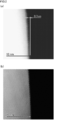
- FIG. 2A is an STEM image of the dielectric material produced in Example 2
- FIG. 2B is an STEM image of the dielectric powder before the processing in Example 2.
- the manufacturing method of the dielectric material of this invention is demonstrated.
- the present invention is not limited to the following configurations, and can be applied with appropriate modifications without departing from the scope of the present invention.
- Each embodiment shown below is an illustration, and it cannot be overemphasized that a partial substitution or combination of composition shown in a different embodiment is possible.
- a combination of two or more of the individual preferable configurations of the present invention described below is also the present invention.
- a dielectric powder, water, an organic acid metal salt, and an alkoxysilane are mixed to prepare a slurry.
- a powder made of a perovskite type compound containing Ba and Ti is preferable.
- the general formula ABO 3 (A site is Ba and may contain at least one selected from the group consisting of Sr and Ca in addition to Ba, and the B site is Ti, In addition to Ti, at least one selected from the group consisting of Zr and Hf may be included, and O is oxygen).
- barium titanate compounds in which barium titanate (that is, BaTiO 3 ) or barium titanate (BaTiO 3 ) is partially substituted with calcium are exemplified. It is done.
- the average particle size of the dielectric powder is preferably 20 nm or more and 300 nm or less. According to the method of the present invention, the metal element and the Si component can be evenly distributed on the surface of the dielectric powder even in such a fine particle size dielectric powder. In the conventional method, it is difficult to uniformly distribute the metal element and the Si component on the surface of the dielectric powder with respect to the dielectric powder having such a fine particle size.
- distilled water ion exchange water, pure water, ultrapure water, or the like is preferably used.
- organic acid metal salt a metal salt soluble in water is used.
- soluble in water means that the organic acid metal salt corresponding to the amount of the metal element added as an additive has a solubility enough to dissolve in water. Since the amount of the metal element added to the dielectric powder is usually a very small amount, the solubility of the organic acid metal salt does not need to be so high. Therefore, even if it is an organic acid metal salt classified as a “slightly soluble salt” in the usual definition, it may be used as an “acid-soluble” organic acid metal salt in this specification.
- the organic acid metal salt is an organic metal salt of at least one organic acid selected from the group consisting of monocarboxylic acids having 6 or less carbon atoms, dicarboxylic acids, trivalent or higher polyvalent carboxylic acids, and hydroxycarboxylic acids.
- An acid metal salt is mentioned. Only one type of organic acid metal salt can be used, or a plurality of types can be used in combination. For example, two or more metal salts of monocarboxylic acids having 6 or less carbon atoms may be combined, or a metal salt of monocarboxylic acids having 6 or less carbon atoms and a metal salt of hydroxycarboxylic acid may be combined.
- organic acid metal salts when two or more kinds of organic acid metal salts are combined, a combination of two or more kinds of organic acid metal salts having different kinds of organic acids and the same kind of metal element may be used. It may be a combination of two or more organic acid metal salts that are the same and have different types of metal elements.
- organic acid the following organic acids are preferable.
- monocarboxylic acid having 6 or less carbon atoms formic acid, acetic acid and propionic acid are preferable, and acetic acid is more preferable.
- the dicarboxylic acid a dicarboxylic acid having 6 or less carbon atoms is preferable, and oxalic acid, malonic acid, succinic acid, fumaric acid, maleic acid and glutaric acid are more preferable.
- the polyvalent carboxylic acid is preferably a polyvalent carboxylic acid having 6 or less carbon atoms.
- hydroxycarboxylic acid a hydroxycarboxylic acid having 6 or less carbon atoms is preferable, and lactic acid, citric acid, malic acid, tartaric acid and gluconic acid are more preferable.
- those having one carboxy group lactic acid, gluconic acid
- those having two carboxy groups malic acid, tartaric acid
- those having three or more carboxy groups are polyvalent carboxylic acids.
- the metal element contained in the organic acid metal salt is at least one of Dy, Gd, Y, Mn, Mg, Sr, Nb, Nd, V, Co, Ni, Ce, Er, Ca, Ba, and Li. It is preferable. By adding these metal elements as additives, the electrical properties and sinterability of the dielectric material are improved. Among these, at least one of Dy, Mn, and Mg is more preferable.
- any combination of the organic acid and the metal element contained in the organic acid metal salt is possible.
- Preferred combinations include dysprosium acetate, manganese acetate, and magnesium acetate.
- Alkoxysilane as a silicon compound has four alkoxy groups.
- the alkoxysilane is represented by the general formula (1).
- Si- (OR) 4 (1) (In general formula (1), R is a methyl group or an ethyl group, and four Rs may be the same or different.)
- Preferred alkoxysilanes include tetraethoxysilane (TEOS) in which all four R are ethyl groups, and tetramethoxysilane (TMOS) in which all four R are methyl groups, and tetraethoxysilane (TEOS) is more preferable. .
- alkoxysilanes are not dissolved in water as they are, but silicon compounds obtained by hydrolyzing at least one of the four alkoxy groups can be dissolved in water.
- a silicon compound obtained by hydrolyzing at least one of four alkoxy groups of alkoxysilane is represented by the following general formula (2).
- n is an integer of 1 or more and 4 or less.
- R is a methyl group or an ethyl group.
- the silicon compound has a plurality of Rs. In this case, R may be the same or different.
- the number n of hydrolyzed alkoxy groups does not have to be the same, and n may be different.
- the aqueous slurry is preferably an alkaline slurry.
- the alkaline slurry is used, hydrolysis of the alkoxysilane is promoted, so that the treatment time for hydrolyzing the alkoxysilane is shortened, and the production efficiency of the dielectric material can be improved.
- the pH of the slurry is preferably 10 or more and 13 or less. It is preferable for the pH to be in the above range because the hydrolysis is promoted and the condensation reaction does not proceed so much, so that the SiO 2 particles hardly precipitate.
- the method for preparing the alkaline slurry is not particularly limited as long as the dielectric powder, water, organic acid metal salt, alkoxysilane and the alkali component can be mixed, and the mixing order of the components is also not limited. It is not particularly limited.
- As the alkaline component an alkaline aqueous solution can be used, and aqueous ammonia can be preferably used. When ammonia water is used, ammonia easily volatilizes, so that it is possible to suppress the alkaline component from remaining in the dielectric material and degrading the characteristics of the dielectric material.
- an alkoxysilane and an alkaline aqueous solution are mixed to prepare an alkaline alkoxysilane solution, and the alkaline alkoxysilane solution is mixed with dielectric powder, water, and an organic acid metal salt.
- a method of preparing an alkaline slurry (alkaline slurry preparing method 1).
- the method (alkaline slurry preparation method 2) which mixes dielectric powder, water, organic acid metal salt, and alkoxysilane, prepares a slurry, and also prepares an alkaline slurry by adding alkaline aqueous solution is also mentioned.
- hydrolysis of the alkoxysilane can be promoted by addition of the alkaline aqueous solution, so that the treatment time until the aqueous slurry is made can be shortened.
- the retention time from mixing the alkoxysilane and the alkaline aqueous solution to preparing the alkaline alkoxysilane solution and mixing with the other components is preferably 20 minutes or less. It is more preferable that When the holding time is 20 minutes or less, the condensation reaction is prevented from occurring following the hydrolysis, and the slurry can be prevented from becoming clouded.
- the drying step the slurry is dried to obtain a dielectric powder.
- the organic acid metal salt contained in the slurry and the silicon compound obtained by hydrolyzing the alkoxysilane are uniformly attached.
- a dielectric material in which the metal element and the Si component are uniformly distributed on the surface of the dielectric powder can be manufactured.
- drying method in the drying process is not particularly limited, but drying using a rotary evaporator that dries the slurry while stirring, thin film drying using a drum dryer or the like that instantaneously dries, and fine droplets Spray drying such as drying is preferred. Among these, spray drying is more preferable. Moreover, when drying while heating, it is preferable that drying temperature is 40 degreeC or more and 250 degrees C or less.
- the dielectric material manufactured by the dielectric material manufacturing method of the present invention is suitable as a raw material powder for the dielectric layer of the multilayer ceramic capacitor.
- an organic binder, a plasticizer and an organic solvent are added to the dielectric material produced by the dielectric material production method of the present invention, if necessary, and mixed using a ball mill or the like. Prepare the rally.
- a ceramic green sheet using the ceramic slurry formation of a conductive paste film to be an internal electrode layer, lamination and firing of the ceramic green sheet formed with the conductive paste film, A laminated body having a plurality of internal electrode layers is obtained.
- a multilayer ceramic capacitor can be manufactured by forming external electrodes on both end faces of the multilayer body.
- known techniques and process conditions can be used.
- the firing conditions after the lamination of the ceramic green sheets are 1150 ° C. or more and 1350 ° C. or less, and a reduction consisting of H 2 —N 2 —H 2 O gas having an oxygen partial pressure of 10 ⁇ 9 MPa or less and 10 ⁇ 12 MPa or more.
- a method for forming the external electrode a method may be mentioned in which a conductive paste layer to be an external electrode is applied and formed before firing the ceramic green sheet, and the conductive paste layer is baked in accordance with the firing of the laminate.
- Example 1 1.76 g of dysprosium acetate and 0.53 g of manganese acetate were added to 300 g of water and mixed and stirred to prepare an aqueous solution in which dysprosium acetate and manganese acetate were dissolved in water.
- a slurry was prepared by adding 100 g of barium titanate particles (hereinafter referred to as BT particles) having an average particle diameter of 150 nm to this aqueous solution.
- BT particles barium titanate particles
- TEOS tetraethoxysilane
- the slurry was allowed to stand, but separation of TEOS was not confirmed, and it was confirmed that TEOS hydrolysis proceeded.
- the slurry is then evaporated to dryness with a spray dryer and heat treated at 500 ° C. to decompose dysprosium acetate and manganese acetate, and this powder is subjected to scanning transmission electron microscope-energy dispersive X-ray spectroscopy (STEM-EDX). As a result of confirmation, it was confirmed that Si, Dy, and Mn were uniformly distributed on the surface of the BT particles.
- STEM-EDX scanning transmission electron microscope-energy dispersive X-ray spectroscopy
- Example 2 1.76 g of dysprosium acetate and 0.53 g of manganese acetate were added to 230 g of water and mixed and stirred to prepare an aqueous solution in which dysprosium acetate and manganese acetate were dissolved in water. 100 g of BT particles having an average particle size of 150 nm were added to this aqueous solution to prepare a slurry of BT particles. Separately, 1.9 g of TEOS was added to 70 g of 1N ammonia water while stirring, and the mixture stirred for 10 minutes was mixed with the previously prepared slurry of BT particles and stirred for 30 minutes. And evaporated to dryness.
- the obtained powder was put into a hexametaphosphoric acid aqueous solution so as to be 0.6 g / L and dispersed with a 300 W ultrasonic disperser, and image analysis was performed using a wet flow type particle size / shape analyzer.
- the coarsening rate was 0.16%.
- dysprosium octylate and manganese octylate are insoluble in water, they could not be uniformly coated on the surface of the BT particles.
- TEOS seemed to remain separated without being fully hydrolyzed. This is probably because TEOS is water-insoluble and the hydrolysis rate is slow in the aqueous slurry.
- the slurry was evaporated and dried by a rotary evaporator, and further heat-treated at 500 ° C.
- the distribution of Si, Dy, and Mn on the surface of this powder was confirmed by STEM-EDX.
- the obtained powder was image-analyzed in the same manner as in Example 2 and the proportion of coarse particles having a particle size of 1 ⁇ m or more (coarseness rate) was confirmed.
- the coarsening rate was as high as 0.25%. .
- the slurry was evaporated to dryness with a spray dryer and further heat-treated at 500 ° C.
- the distribution of Si, Dy, and Mn on the surface of this powder was confirmed by STEM-EDX.
- the obtained powder was subjected to image analysis in the same manner as in Example 2 and the proportion of coarse particles having a particle size of 1 ⁇ m or more (coarseness rate) was confirmed.
- the coarseness rate was 0.30%, It was quite expensive. This is because the metal sol (that is, the water-soluble dysprosium sol and the water-soluble manganese sol) uses an organic substance for stabilizing the particles. The rate seems to have increased.
- FIG. 1A, FIG. 1B, and FIG. 1C are STEM-EDX mapping images of the surface of the dielectric material produced in Example 2, Comparative Example 2, and Comparative Example 3, respectively.
- STEM “JEM-2200FS” manufactured by JEOL Ltd. is used, and the acceleration voltage is 200 kV.
- Detector EDX (EDS) the Japan Electronics Co., Ltd. "JED-2300T” is used, using the SDD detector of 60mm 2 caliber, EDX system, Thermo Fisher Scientific, Inc. "Noran System 7" is used .
- Example 2 shown in FIG. 1B Comparative Example 2 shown in FIG. 1B is slightly inferior in uniformity (particularly Dy) as compared to Example 2. Further, since ethanol and toluene, which are organic solvents, are used as solvents, this is also a disadvantageous method.
- the comparative example 3 shown in FIG.1 (c) is largely inferior in uniformity for each element. This is due to the use of sol as each element source.
- FIG. 2A is an STEM image of the dielectric material produced in Example 2
- FIG. 2B is an STEM image of the dielectric powder before the processing in Example 2.
- the STEM image was taken at an acceleration voltage of 200 kV using an ARM-200F manufactured by JEOL. From this photograph, it was confirmed that an amorphous layer having a thickness of about 0.7 nm was uniformly formed on the surface of the BT particles.
Landscapes
- Engineering & Computer Science (AREA)
- Chemical & Material Sciences (AREA)
- Ceramic Engineering (AREA)
- Manufacturing & Machinery (AREA)
- Materials Engineering (AREA)
- Structural Engineering (AREA)
- Organic Chemistry (AREA)
- Inorganic Chemistry (AREA)
- Power Engineering (AREA)
- Microelectronics & Electronic Packaging (AREA)
- Ceramic Capacitors (AREA)
- Inorganic Insulating Materials (AREA)
Abstract
本発明の誘電体材料の製造方法は、誘電体粉末と、水と、炭素数6以下のモノカルボン酸、ジカルボン酸、3価以上の多価カルボン酸及びヒドロキシカルボン酸からなる群から選択された少なくとも1種の有機酸の金属塩である有機酸金属塩と、下記一般式(1)で表されるアルコキシシランとを混合してスラリーを準備する準備工程と、上記スラリーを乾燥して誘電体粉末を得る乾燥工程と、を含むことを特徴とする。 Si-(OR)4 (1) (一般式(1)中、Rはメチル基又はエチル基であり、4つのRは同一であっても異なっていてもよい。)
Description
本発明は、誘電体材料の製造方法に関する。
積層セラミックコンデンサ(以下、MLCCとも表記)の誘電体層を形成するための誘電体材料の製造方法としては、チタン酸バリウムなどの基本粉末に種々の金属化合物を混合し、分散させることが知られている。これらの金属化合物は、誘電体材料の電気特性や焼結性を向上するために混合されている。金属化合物は、金属の炭酸塩及び金属酸化物を含む。
近年のMLCCは小型化しており、誘電体層は薄層化が要求されている。そのため、誘電体材料の微粒化が必要となっているが、基本粉末と微量の金属化合物とを粉末同士で混合させてもミクロに均一分散させることは困難となっている。
近年のMLCCは小型化しており、誘電体層は薄層化が要求されている。そのため、誘電体材料の微粒化が必要となっているが、基本粉末と微量の金属化合物とを粉末同士で混合させてもミクロに均一分散させることは困難となっている。
特許文献1には、有機溶媒中で、疎水性金属塩と、ケイ素化合物としてのシランカップリング剤と、基本粉末とを混合することにより、添加する金属元素を基本粉末に均一に分散させるようにする技術が開示されている。
特許文献2には、ケイ素化合物としてシリカゾルを用いて水系スラリーを調製し、誘電体材料粉末を製造する技術が開示されている。
特許文献1に記載された技術では、有機溶媒を用いるため、誘電体材料の製造にあたり防爆装置、防爆施設が必要であり、製造コストを抑えることが困難となっている。
また、シランカップリング剤として用いているテトラエトキシシラン(TEOS)などの有機溶媒に可溶な安価なSiアルコキシドは、乾燥時に揮発するため、ゾルとして安定化させるための有機物を添加する必要がある。
上記有機物を添加すると、上記有機物を含んだ粉末を成形し焼成する際に成形用バインダーとの反応による成形体への不具合や有機物の分解による焼結体へのクラックの発生などの不具合を引き起こすため、成形する前に誘電体材料粉末中の有機物を分解除去する熱処理工程が設けられることが一般的である。この熱処理時に有機物の分解における発熱で焼結が促進され、粗大粒子が生成しやすくなり、製造された誘電体材料粒子の分散性が悪化するなどの問題がある。
また、シランカップリング剤として用いているテトラエトキシシラン(TEOS)などの有機溶媒に可溶な安価なSiアルコキシドは、乾燥時に揮発するため、ゾルとして安定化させるための有機物を添加する必要がある。
上記有機物を添加すると、上記有機物を含んだ粉末を成形し焼成する際に成形用バインダーとの反応による成形体への不具合や有機物の分解による焼結体へのクラックの発生などの不具合を引き起こすため、成形する前に誘電体材料粉末中の有機物を分解除去する熱処理工程が設けられることが一般的である。この熱処理時に有機物の分解における発熱で焼結が促進され、粗大粒子が生成しやすくなり、製造された誘電体材料粒子の分散性が悪化するなどの問題がある。
特許文献2では、ケイ素化合物としてシリカゾルが用いられている。シリカゾルの粒子径は通常は5~20nm程度であり、あるpH領域でのみ分散安定な状態となる。そのため、各種金属塩の添加の際にケイ素化合物の凝集が起こり、ミクロな均一コーティングが困難となるなどの問題がある。
また、シリカゾルの安定化のために各種有機物が多く含有されている。そのため、熱処理時に有機物の分解における発熱で焼結が促進され、粗大粒子が生成しやすくなり、製造された誘電体材料粒子の分散性が悪化するなどの問題がある。
また、シリカゾルの安定化のために各種有機物が多く含有されている。そのため、熱処理時に有機物の分解における発熱で焼結が促進され、粗大粒子が生成しやすくなり、製造された誘電体材料粒子の分散性が悪化するなどの問題がある。
本発明は上記の課題を解決するためになされたものであり、水系スラリーを用いて、金属元素とSi成分を誘電体粉末の表面に均一分布させた誘電体材料を製造する方法を提供することを目的とする。
上記目的を達成するための、本発明の誘電体材料の製造方法は、
誘電体粉末と、水と、炭素数6以下のモノカルボン酸、ジカルボン酸、3価以上の多価カルボン酸及びヒドロキシカルボン酸からなる群から選択された少なくとも1種の有機酸の金属塩である有機酸金属塩と、下記一般式(1)で表されるアルコキシシランとを混合してスラリーを準備する準備工程と、
上記スラリーを乾燥して誘電体粉末を得る乾燥工程と、を含むことを特徴とする。
Si-(OR)4 (1)
(一般式(1)中、Rはメチル基又はエチル基であり、4つのRは同一であっても異なっていてもよい。)
誘電体粉末と、水と、炭素数6以下のモノカルボン酸、ジカルボン酸、3価以上の多価カルボン酸及びヒドロキシカルボン酸からなる群から選択された少なくとも1種の有機酸の金属塩である有機酸金属塩と、下記一般式(1)で表されるアルコキシシランとを混合してスラリーを準備する準備工程と、
上記スラリーを乾燥して誘電体粉末を得る乾燥工程と、を含むことを特徴とする。
Si-(OR)4 (1)
(一般式(1)中、Rはメチル基又はエチル基であり、4つのRは同一であっても異なっていてもよい。)
本発明の誘電体材料の製造方法では、有機溶剤を極力必要としないため、防爆装置、防爆施設が不要であり、製造コストを抑えて安全に誘電体材料の製造を行うことができる。なお、防爆装置、防爆設備が不要な範囲内で、スラリーに有機溶剤や界面活性のための有機物を少量加えてもよい。
また、スラリーを準備するにあたり、水に可溶な金属塩である有機酸金属塩を用いているため、金属元素を金属イオンの形で水系スラリー中に溶解させることができる。そのため、誘電体粉末の粒子の表面に金属元素をより均一に分布させることができ、均一な特性を有する信頼性の高い誘電体材料を製造することができる。
また、ケイ素化合物として一般式(1)で表されるアルコキシシランを使用しているが、アルコキシシランはそのままでは水に溶解しにくい。本発明では、有機酸金属塩を使用しており、有機酸金属塩が水系スラリー中で電離した有機酸イオンを触媒として利用し、アルコキシシランの加水分解を促進している。アルコキシシランを加水分解して得られたケイ素化合物は少なくとも一つのヒドロキシル基を有しており、アルコキシシランよりも水に対する溶解度が高い。そのため、水媒質中でアルコキシシランに由来するケイ素化合物の少なくとも一部が分散した状態で、ケイ素化合物を誘電体粉末の粒子の表面に吸着させることができる。
上記のとおり、誘電体粉末を含み、金属元素とアルコキシシラン由来のケイ素化合物とがともに溶解した水系スラリーを調製することができるので、このスラリーを乾燥することによって金属元素とSi成分を誘電体粉末の表面に均一に分布させた誘電体材料を製造することができる。
乾燥工程を経て得られた誘電体材料を熱処理すると、誘電体材料の表面には金属元素とSi成分とが均一に分布したアモルファス膜が形成されている。この材料を用いれば、積層セラミックコンデンサの製造工程における焼結時において、誘電体粉末を構成する結晶粒子内に金属元素を均一に短時間で固溶させることができる。
その結果、信頼性に優れ、かつ、耐電圧特性のバラツキの少ない積層セラミックコンデンサを得ることができる。
また、有機酸金属塩に含まれる有機酸は焼成により除去することができるので、本発明で製造した誘電体材料を焼成して作製したセラミックコンデンサ内に有機酸が残留することがなく、電気特性に悪影響を与えない。
また、スラリーを準備するにあたり、水に可溶な金属塩である有機酸金属塩を用いているため、金属元素を金属イオンの形で水系スラリー中に溶解させることができる。そのため、誘電体粉末の粒子の表面に金属元素をより均一に分布させることができ、均一な特性を有する信頼性の高い誘電体材料を製造することができる。
また、ケイ素化合物として一般式(1)で表されるアルコキシシランを使用しているが、アルコキシシランはそのままでは水に溶解しにくい。本発明では、有機酸金属塩を使用しており、有機酸金属塩が水系スラリー中で電離した有機酸イオンを触媒として利用し、アルコキシシランの加水分解を促進している。アルコキシシランを加水分解して得られたケイ素化合物は少なくとも一つのヒドロキシル基を有しており、アルコキシシランよりも水に対する溶解度が高い。そのため、水媒質中でアルコキシシランに由来するケイ素化合物の少なくとも一部が分散した状態で、ケイ素化合物を誘電体粉末の粒子の表面に吸着させることができる。
上記のとおり、誘電体粉末を含み、金属元素とアルコキシシラン由来のケイ素化合物とがともに溶解した水系スラリーを調製することができるので、このスラリーを乾燥することによって金属元素とSi成分を誘電体粉末の表面に均一に分布させた誘電体材料を製造することができる。
乾燥工程を経て得られた誘電体材料を熱処理すると、誘電体材料の表面には金属元素とSi成分とが均一に分布したアモルファス膜が形成されている。この材料を用いれば、積層セラミックコンデンサの製造工程における焼結時において、誘電体粉末を構成する結晶粒子内に金属元素を均一に短時間で固溶させることができる。
その結果、信頼性に優れ、かつ、耐電圧特性のバラツキの少ない積層セラミックコンデンサを得ることができる。
また、有機酸金属塩に含まれる有機酸は焼成により除去することができるので、本発明で製造した誘電体材料を焼成して作製したセラミックコンデンサ内に有機酸が残留することがなく、電気特性に悪影響を与えない。
本発明の誘電体材料の製造方法では、上記準備工程において、上記スラリーをアルカリ性スラリーとして準備することが好ましい。
アルカリ性スラリーとすると、アルコキシシランの加水分解が促進されるため、アルコキシシランを加水分解するための処理時間が短縮され、誘電体材料の製造効率を向上させることができる。
アルカリ性スラリーとすると、アルコキシシランの加水分解が促進されるため、アルコキシシランを加水分解するための処理時間が短縮され、誘電体材料の製造効率を向上させることができる。
本発明の誘電体材料の製造方法では、上記アルコキシシランとアルカリ性水溶液を混合してアルカリ性アルコキシシラン溶液を調製し、
上記アルカリ性アルコキシシラン溶液を、上記誘電体粉末、上記水及び上記有機酸金属塩と混合することによって、上記アルカリ性スラリーを準備することが好ましい。
アルカリ性スラリーを準備する方法として、アルコキシシランとアルカリ性水溶液を混合しておき、アルコキシシランの加水分解を進めておくと、誘電体粉末、水及び有機酸金属塩と混合した場合に水系スラリーとするまでの処理時間を短くすることができる。
上記アルカリ性アルコキシシラン溶液を、上記誘電体粉末、上記水及び上記有機酸金属塩と混合することによって、上記アルカリ性スラリーを準備することが好ましい。
アルカリ性スラリーを準備する方法として、アルコキシシランとアルカリ性水溶液を混合しておき、アルコキシシランの加水分解を進めておくと、誘電体粉末、水及び有機酸金属塩と混合した場合に水系スラリーとするまでの処理時間を短くすることができる。
また、本発明の誘電体材料の製造方法では、上記誘電体粉末、上記水、上記有機酸金属塩及び上記アルコキシシランを混合してスラリーを調製し、さらにアルカリ性水溶液を加えて上記アルカリ性スラリーを準備することが好ましい。
アルカリ性スラリーを準備する方法として、誘電体粉末、水、有機酸金属塩及びアルコキシシランを混合した後にアルカリ性水溶液を加えても、アルカリ性水溶液の添加によりアルコキシシランの加水分解を促進させることができるため、水系スラリーとするまでの処理時間を短くすることができる。
アルカリ性スラリーを準備する方法として、誘電体粉末、水、有機酸金属塩及びアルコキシシランを混合した後にアルカリ性水溶液を加えても、アルカリ性水溶液の添加によりアルコキシシランの加水分解を促進させることができるため、水系スラリーとするまでの処理時間を短くすることができる。
本発明の誘電体材料の製造方法では、上記乾燥工程における乾燥方法が噴霧乾燥であることが好ましい。
乾燥方法を噴霧乾燥とすることにより、乾燥時に金属元素とSi成分が誘電体粉末の粒子間で偏析することを抑制することができる。
乾燥方法を噴霧乾燥とすることにより、乾燥時に金属元素とSi成分が誘電体粉末の粒子間で偏析することを抑制することができる。
本発明の誘電体材料の製造方法では、上記誘電体粉末が、チタン酸バリウム粉末、又は、チタン酸バリウムのバリウムの一部がカルシウムで置換されたチタン酸バリウム系粉末であることが好ましい。
このような誘電体粉末から形成される誘電体材料は、積層セラミックコンデンサの誘電体層を形成するために好適に使用することができる。
このような誘電体粉末から形成される誘電体材料は、積層セラミックコンデンサの誘電体層を形成するために好適に使用することができる。
本発明の誘電体材料の製造方法では、上記有機酸金属塩に含まれる金属元素が、Dy、Gd、Y、Mn、Mg、Sr、Nb、Nd、V、Co、Ni、Ce、Er、Ca、Ba及びLiのうち少なくとも1種であることが好ましい。
これらの金属元素を添加物として加えることにより、誘電体材料の電気特性や焼結性が向上する。
これらの金属元素を添加物として加えることにより、誘電体材料の電気特性や焼結性が向上する。
本発明の誘電体材料の製造方法では、上記有機酸が酢酸であることが好ましい。
酢酸金属塩は、一般的に水への溶解性が高いので、水系スラリー中に金属元素を溶解させるための原料として適している。
酢酸金属塩は、一般的に水への溶解性が高いので、水系スラリー中に金属元素を溶解させるための原料として適している。
この発明によれば、金属元素とSi成分を誘電体粉末の表面に均一に分布させた誘電体材料を製造することができる。
以下、本発明の誘電体材料の製造方法について説明する。
しかしながら、本発明は、以下の構成に限定されるものではなく、本発明の要旨を変更しない範囲において適宜変更して適用することができる。
以下に示す各実施形態は例示であり、異なる実施形態で示した構成の部分的な置換又は組み合わせが可能であることは言うまでもない。
以下において記載する本発明の個々の好ましい構成を2つ以上組み合わせたものもまた本発明である。
しかしながら、本発明は、以下の構成に限定されるものではなく、本発明の要旨を変更しない範囲において適宜変更して適用することができる。
以下に示す各実施形態は例示であり、異なる実施形態で示した構成の部分的な置換又は組み合わせが可能であることは言うまでもない。
以下において記載する本発明の個々の好ましい構成を2つ以上組み合わせたものもまた本発明である。
(1)スラリーを準備する準備工程
まず、誘電体粉末と、水と、有機酸金属塩と、アルコキシシランとを混合してスラリーを準備する。
誘電体粉末としては、Ba及びTiを含むペロブスカイト型化合物からなる粉末が好ましい。具体的には、一般式ABO3(AサイトはBaであって、Ba以外にSr及びCaからなる群より選ばれる少なくとも1種を含んでいてもよく、また、BサイトはTiであって、Ti以外にZr及びHfからなる群より選ばれる少なくとも1種を含んでいてもよく、Oは酸素)で表されるペロブスカイト型化合物が挙げられる。
そして、上記ぺロブスカイト型化合物の好ましい例としては、チタン酸バリウム(つまり、BaTiO3)、又は、チタン酸バリウム(BaTiO3)のバリウムの一部がカルシウムで置換されたチタン酸バリウム系化合物が挙げられる。
まず、誘電体粉末と、水と、有機酸金属塩と、アルコキシシランとを混合してスラリーを準備する。
誘電体粉末としては、Ba及びTiを含むペロブスカイト型化合物からなる粉末が好ましい。具体的には、一般式ABO3(AサイトはBaであって、Ba以外にSr及びCaからなる群より選ばれる少なくとも1種を含んでいてもよく、また、BサイトはTiであって、Ti以外にZr及びHfからなる群より選ばれる少なくとも1種を含んでいてもよく、Oは酸素)で表されるペロブスカイト型化合物が挙げられる。
そして、上記ぺロブスカイト型化合物の好ましい例としては、チタン酸バリウム(つまり、BaTiO3)、又は、チタン酸バリウム(BaTiO3)のバリウムの一部がカルシウムで置換されたチタン酸バリウム系化合物が挙げられる。
誘電体粉末の平均粒径は20nm以上、300nm以下であることが好ましい。
本発明の方法であると、このような微細な粒径の誘電体粉末に対しても金属元素とSi成分を誘電体粉末の表面に均一に分布させることができる。
従来の方法ではこのような微細な粒径の誘電体粉末に対して金属元素とSi成分を誘電体粉末の表面に均一に分布させることは難しい。
本発明の方法であると、このような微細な粒径の誘電体粉末に対しても金属元素とSi成分を誘電体粉末の表面に均一に分布させることができる。
従来の方法ではこのような微細な粒径の誘電体粉末に対して金属元素とSi成分を誘電体粉末の表面に均一に分布させることは難しい。
水としては、蒸留水、イオン交換水、純水、超純水等を使用することが好ましい。
有機酸金属塩としては、水に可溶な金属塩を使用する。本明細書における「水に可溶」とは、添加物として加える金属元素の量に相当する有機酸金属塩が水に溶解できる程度の溶解度を有することを意味する。
誘電体粉末に対して加える金属元素の量は通常は微量であるので、有機酸金属塩の溶解度としてはそれほど高い値である必要はない。そのため、通常の定義では「難溶性塩」に分類される有機酸金属塩であっても、本明細書における「水に可溶」の有機酸金属塩として使用できる場合はある。
誘電体粉末に対して加える金属元素の量は通常は微量であるので、有機酸金属塩の溶解度としてはそれほど高い値である必要はない。そのため、通常の定義では「難溶性塩」に分類される有機酸金属塩であっても、本明細書における「水に可溶」の有機酸金属塩として使用できる場合はある。
有機酸金属塩としては、炭素数6以下のモノカルボン酸、ジカルボン酸、3価以上の多価カルボン酸及びヒドロキシカルボン酸からなる群から選択された少なくとも1種の有機酸の金属塩である有機酸金属塩が挙げられる。
有機酸金属塩は1種類のみを使用することもでき、複数の種類を組み合わせて使用することもできる。例えば、炭素数6以下のモノカルボン酸の金属塩を2種類以上組み合わせてもよいし、炭素数6以下のモノカルボン酸の金属塩とヒドロキシカルボン酸の金属塩を組み合わせてもよい。
また、有機酸金属塩を2種類以上組み合わせる際には、有機酸の種類が異なり金属元素の種類が同一である2種類以上の有機酸金属塩の組み合わせであってもよく、有機酸の種類が同一で金属元素の種類が異なる2種類以上の有機酸金属塩の組み合わせであってもよい。
有機酸金属塩は1種類のみを使用することもでき、複数の種類を組み合わせて使用することもできる。例えば、炭素数6以下のモノカルボン酸の金属塩を2種類以上組み合わせてもよいし、炭素数6以下のモノカルボン酸の金属塩とヒドロキシカルボン酸の金属塩を組み合わせてもよい。
また、有機酸金属塩を2種類以上組み合わせる際には、有機酸の種類が異なり金属元素の種類が同一である2種類以上の有機酸金属塩の組み合わせであってもよく、有機酸の種類が同一で金属元素の種類が異なる2種類以上の有機酸金属塩の組み合わせであってもよい。
有機酸としては、以下の有機酸が好ましい。
炭素数6以下のモノカルボン酸としては、ギ酸、酢酸及びプロピオン酸が好ましく、酢酸がより好ましい。
炭素数6以下のモノカルボン酸としては、ギ酸、酢酸及びプロピオン酸が好ましく、酢酸がより好ましい。
ジカルボン酸としては、炭素数6以下のジカルボン酸が好ましく、シュウ酸、マロン酸、コハク酸、フマル酸、マレイン酸及びグルタル酸がより好ましい。多価カルボン酸としては、炭素数6以下の多価カルボン酸が好ましい。
ヒドロキシカルボン酸としては、炭素数6以下のヒドロキシカルボン酸が好ましく、乳酸、クエン酸、リンゴ酸、酒石酸及びグルコン酸がより好ましい。
また、上記ヒドロキシカルボン酸のうち、カルボキシ基が1つのもの(乳酸、グルコン酸)は炭素数6以下のモノカルボン酸でもあり、カルボキシ基が2つのもの(リンゴ酸、酒石酸)はジカルボン酸でもあり、カルボキシ基が3つ以上のもの(クエン酸)は多価カルボン酸であるともいえる。
また、上記ヒドロキシカルボン酸のうち、カルボキシ基が1つのもの(乳酸、グルコン酸)は炭素数6以下のモノカルボン酸でもあり、カルボキシ基が2つのもの(リンゴ酸、酒石酸)はジカルボン酸でもあり、カルボキシ基が3つ以上のもの(クエン酸)は多価カルボン酸であるともいえる。
有機酸金属塩に含まれる金属元素としては、Dy、Gd、Y、Mn、Mg、Sr、Nb、Nd、V、Co、Ni、Ce、Er、Ca、Ba及びLiのうち少なくとも1種であることが好ましい。これらの金属元素を添加物として加えることにより、誘電体材料の電気特性や焼結性が向上する。
これらの中でも、Dy、Mn及びMgのうち少なくとも1種であることがより好ましい。
これらの中でも、Dy、Mn及びMgのうち少なくとも1種であることがより好ましい。
また、有機酸金属塩に含まれる有機酸と金属元素の組み合わせとしては、上記有機酸と上記金属元素のいずれの組み合わせも可能である。好ましい組み合わせとして、酢酸ディスプロシウム、酢酸マンガン、酢酸マグネシウムが挙げられる。
ケイ素化合物としてのアルコキシシランは、アルコキシ基を4つ有する。アルコキシシランは一般式(1)で表される。
Si-(OR)4 (1)
(一般式(1)中、Rはメチル基又はエチル基であり、4つのRは同一であっても異なっていてもよい。)
好ましいアルコキシシランとしては、4つのRが全てエチル基であるテトラエトキシシラン(TEOS)、4つのRが全てメチル基であるテトラメトキシシラン(TMOS)が挙げられ、テトラエトキシシラン(TEOS)がより好ましい。
これらのアルコキシシランはそのままでは水に溶解しないが、4つのアルコキシ基のうち少なくとも1つを加水分解して得られるケイ素化合物は水に溶解することができる。
アルコキシシランの4つのアルコキシ基のうち少なくとも1つを加水分解して得られるケイ素化合物は、以下の一般式(2)で表される。
(HO)n-Si-(OR)4-n (2)
一般式(2)中、nは1以上4以下の整数である。Rはメチル基又はエチル基である。nが1又は2の場合、ケイ素化合物は複数のRを有する。この場合、Rは同一であっても異なっていてもよい。さらに加水分解したアルコキシ基の数nはすべてが同一である必要はなく、nが異なる状態でもよい。
Si-(OR)4 (1)
(一般式(1)中、Rはメチル基又はエチル基であり、4つのRは同一であっても異なっていてもよい。)
好ましいアルコキシシランとしては、4つのRが全てエチル基であるテトラエトキシシラン(TEOS)、4つのRが全てメチル基であるテトラメトキシシラン(TMOS)が挙げられ、テトラエトキシシラン(TEOS)がより好ましい。
これらのアルコキシシランはそのままでは水に溶解しないが、4つのアルコキシ基のうち少なくとも1つを加水分解して得られるケイ素化合物は水に溶解することができる。
アルコキシシランの4つのアルコキシ基のうち少なくとも1つを加水分解して得られるケイ素化合物は、以下の一般式(2)で表される。
(HO)n-Si-(OR)4-n (2)
一般式(2)中、nは1以上4以下の整数である。Rはメチル基又はエチル基である。nが1又は2の場合、ケイ素化合物は複数のRを有する。この場合、Rは同一であっても異なっていてもよい。さらに加水分解したアルコキシ基の数nはすべてが同一である必要はなく、nが異なる状態でもよい。
中性領域ではアルコキシ基の加水分解速度が遅いため、水系スラリーをアルカリ性スラリーとすることが好ましい。
アルカリ性スラリーとすると、アルコキシシランの加水分解が促進されるため、アルコキシシランを加水分解するための処理時間が短縮され、誘電体材料の製造効率を向上させることができる。
アルコキシシランの加水分解を促進するためには、スラリーのpHを10以上13以下にすることが好ましい。
pHが上記範囲内であると、加水分解が促進され、かつ、縮合反応がそれほど進まないのでSiO2粒子が析出しにくいために好ましい。
アルカリ性スラリーとすると、アルコキシシランの加水分解が促進されるため、アルコキシシランを加水分解するための処理時間が短縮され、誘電体材料の製造効率を向上させることができる。
アルコキシシランの加水分解を促進するためには、スラリーのpHを10以上13以下にすることが好ましい。
pHが上記範囲内であると、加水分解が促進され、かつ、縮合反応がそれほど進まないのでSiO2粒子が析出しにくいために好ましい。
アルカリ性スラリーを準備する方法としては、誘電体粉末、水、有機酸金属塩、アルコキシシランと、アルカリ成分を混合することのできる方法であれば特に限定されるものではなく、各成分の混合順序も特に限定されるものではない。
アルカリ成分としては、アルカリ性水溶液を使用することができ、アンモニア水を好適に使用することができる。
アンモニア水を使用した場合、アンモニアは揮発しやすいため、アルカリ成分が誘電体材料に残留して誘電体材料の特性を低下させることを抑制することができる。また、アンモニア水を使用した場合、焼成時に発熱することが少なく、局所的な発熱による粒子同士の焼結を抑制することができ、粗粒が少なく平均粒径の小さい誘電体材料の粉末を得ることができる。
アルカリ成分としては、アルカリ性水溶液を使用することができ、アンモニア水を好適に使用することができる。
アンモニア水を使用した場合、アンモニアは揮発しやすいため、アルカリ成分が誘電体材料に残留して誘電体材料の特性を低下させることを抑制することができる。また、アンモニア水を使用した場合、焼成時に発熱することが少なく、局所的な発熱による粒子同士の焼結を抑制することができ、粗粒が少なく平均粒径の小さい誘電体材料の粉末を得ることができる。
アルカリ性スラリーを準備する方法の具体例としては、アルコキシシランとアルカリ性水溶液を混合してアルカリ性アルコキシシラン溶液を調製し、アルカリ性アルコキシシラン溶液を、誘電体粉末、水及び有機酸金属塩と混合することによって、アルカリ性スラリーを準備する方法(アルカリ性スラリー準備方法1)が挙げられる。
また、誘電体粉末、水、有機酸金属塩及びアルコキシシランを混合してスラリーを調製し、さらにアルカリ性水溶液を加えてアルカリ性スラリーを準備する方法(アルカリ性スラリー準備方法2)も挙げられる。
アルカリ性スラリー準備方法1、2のいずれの方法であっても、アルカリ性水溶液の添加によりアルコキシシランの加水分解を促進させることができるため、水系スラリーとするまでの処理時間を短くすることができる。
また、誘電体粉末、水、有機酸金属塩及びアルコキシシランを混合してスラリーを調製し、さらにアルカリ性水溶液を加えてアルカリ性スラリーを準備する方法(アルカリ性スラリー準備方法2)も挙げられる。
アルカリ性スラリー準備方法1、2のいずれの方法であっても、アルカリ性水溶液の添加によりアルコキシシランの加水分解を促進させることができるため、水系スラリーとするまでの処理時間を短くすることができる。
上記アルカリ性スラリー準備方法1において、アルコキシシランとアルカリ性水溶液を混合してアルカリ性アルコキシシラン溶液を調製してから、他の成分と混合するまでの保持時間は20分以下であることが好ましく、10分以下であることがより好ましい。
上記保持時間が20分以下であると、加水分解に続いて縮合反応が生じることが防止され、スラリーが白濁化することを抑制することができる。
上記保持時間が20分以下であると、加水分解に続いて縮合反応が生じることが防止され、スラリーが白濁化することを抑制することができる。
(2)乾燥工程
乾燥工程では、スラリーを乾燥して誘電体粉末を得る。
乾燥工程で乾燥させる誘電体粉末の表面には、スラリー中に含まれる有機酸金属塩とアルコキシシランを加水分解して得られたケイ素化合物とが均一に付着している。
この誘電体粉末を乾燥することによって、金属元素とSi成分を誘電体粉末の表面に均一に分布させた誘電体材料を製造することができる。
乾燥工程では、スラリーを乾燥して誘電体粉末を得る。
乾燥工程で乾燥させる誘電体粉末の表面には、スラリー中に含まれる有機酸金属塩とアルコキシシランを加水分解して得られたケイ素化合物とが均一に付着している。
この誘電体粉末を乾燥することによって、金属元素とSi成分を誘電体粉末の表面に均一に分布させた誘電体材料を製造することができる。
また、乾燥工程における乾燥方法は特に限定されるものではないが、スラリーを撹拌しながら乾燥するロータリーエバポレータ等を用いた乾燥や、瞬時に乾燥するドラムドライヤー等を用いた薄膜乾燥や、微粒液滴乾燥等の噴霧乾燥であることが好ましい。これらのなかでも噴霧乾燥がより好ましい。
また、加熱しながら乾燥を行う場合は、乾燥温度は40℃以上、250℃以下であることが好ましい。
また、加熱しながら乾燥を行う場合は、乾燥温度は40℃以上、250℃以下であることが好ましい。
本発明の誘電体材料の製造方法で製造された誘電体材料は、積層セラミックコンデンサの誘電体層の原料粉末として適している。
積層セラミックコンデンサを製造する場合、本発明の誘電体材料の製造方法で製造された誘電体材料に、必要に応じて有機バインダー、可塑剤及び有機溶剤を加えてボールミル等を用いて混合し、セラミックスラリーを調製する。
積層セラミックコンデンサを製造する場合、本発明の誘電体材料の製造方法で製造された誘電体材料に、必要に応じて有機バインダー、可塑剤及び有機溶剤を加えてボールミル等を用いて混合し、セラミックスラリーを調製する。
その後、上記セラミックスラリーを用いたセラミックグリーンシートの作製、内部電極層となるべき導電性ペースト膜の形成、導電性ペースト膜を形成したセラミックグリーンシートの積層及び焼成を行い、誘電体セラミック層と複数の内部電極層とを有する積層体を得る。
最後に、積層体の両端面に外部電極を形成することにより積層セラミックコンデンサを製造することができる。
これらの各工程においては公知の技術及び工程条件を使用することができる。
なお、セラミックグリーンシートの積層後の焼成条件は、1150℃以上、1350℃以下で、酸素分圧10-9MPa以下、10-12MPa以上のH2-N2-H2Oガスからなる還元性雰囲気中で行うことが好ましい。
また、外部電極の形成方法としては、セラミックグリーンシートの焼成前に外部電極となる導電性ペースト層を塗布形成しておき、積層体の焼成時に合わせて導電性ペースト層を焼き付ける方法も挙げられる。
最後に、積層体の両端面に外部電極を形成することにより積層セラミックコンデンサを製造することができる。
これらの各工程においては公知の技術及び工程条件を使用することができる。
なお、セラミックグリーンシートの積層後の焼成条件は、1150℃以上、1350℃以下で、酸素分圧10-9MPa以下、10-12MPa以上のH2-N2-H2Oガスからなる還元性雰囲気中で行うことが好ましい。
また、外部電極の形成方法としては、セラミックグリーンシートの焼成前に外部電極となる導電性ペースト層を塗布形成しておき、積層体の焼成時に合わせて導電性ペースト層を焼き付ける方法も挙げられる。
以下、本発明の誘電体材料の製造方法をより具体的に開示した実施例を示す。なお、本発明は、これらの実施例のみに限定されるものではない。
(実施例1)
水300g中に1.76gの酢酸ディスプロシウム、0.53gの酢酸マンガンを添加して混合攪拌させ、酢酸ディスプロシウム及び酢酸マンガンが水に溶解した水溶液を調製した。この水溶液に平均粒径150nmのチタン酸バリウムの粒子(以下、BT粒子と称する)100gを添加してスラリーを調製した。調製したスラリー中に、攪拌しながら1.9gのテトラエトキシシラン(以下、TEOSと称する)を添加し、8時間攪拌を実施した。その後スラリーを静置したが、TEOSの分離は確認されず、TEOSの加水分解が進んだことを確認した。その後、スラリーを噴霧乾燥器で蒸発乾燥し、500℃で熱処理し酢酸ディスプロシウム及び酢酸マンガンを分解させ、この粉末を走査透過型電子顕微鏡-エネルギー分散型X線分光法(STEM-EDX)で確認したところBT粒子表面にSi,Dy,Mnが均一に分布している様子を確認できた。
さらに波長分散型蛍光X線分析(WDX)のマッピングにて粒子間でのDy,Mn,Siの分布も確認したが、これらDy,Mn,Siの偏析は確認されなかった。ICP発光分光分析法を用いて組成分析を行ったところ、分析されたSi,Dy,Mnの量が、各投入量と誤差10%以内で一致した。
水300g中に1.76gの酢酸ディスプロシウム、0.53gの酢酸マンガンを添加して混合攪拌させ、酢酸ディスプロシウム及び酢酸マンガンが水に溶解した水溶液を調製した。この水溶液に平均粒径150nmのチタン酸バリウムの粒子(以下、BT粒子と称する)100gを添加してスラリーを調製した。調製したスラリー中に、攪拌しながら1.9gのテトラエトキシシラン(以下、TEOSと称する)を添加し、8時間攪拌を実施した。その後スラリーを静置したが、TEOSの分離は確認されず、TEOSの加水分解が進んだことを確認した。その後、スラリーを噴霧乾燥器で蒸発乾燥し、500℃で熱処理し酢酸ディスプロシウム及び酢酸マンガンを分解させ、この粉末を走査透過型電子顕微鏡-エネルギー分散型X線分光法(STEM-EDX)で確認したところBT粒子表面にSi,Dy,Mnが均一に分布している様子を確認できた。
さらに波長分散型蛍光X線分析(WDX)のマッピングにて粒子間でのDy,Mn,Siの分布も確認したが、これらDy,Mn,Siの偏析は確認されなかった。ICP発光分光分析法を用いて組成分析を行ったところ、分析されたSi,Dy,Mnの量が、各投入量と誤差10%以内で一致した。
(実施例2)
水230g中に1.76gの酢酸ディスプロシウム、0.53gの酢酸マンガンを添加して混合攪拌させ、酢酸ディスプロシウム及び酢酸マンガンが水に溶解した水溶液を調製した。この水溶液に平均粒径150nmのBT粒子100gを添加してBT粒子のスラリーを調製した。別途1Nのアンモニア水70g中に攪拌しながら1.9gのTEOSを添加し、10分攪拌したものを、先に調製したBT粒子のスラリーと混合して30分攪拌し、直後に、噴霧乾燥器で蒸発乾燥した。そして、500℃で熱処理し酢酸ディスプロシウム及び酢酸マンガンを分解させた。この粉末をSTEM-EDXで確認したところBT粒子表面にSi,Dy,Mnが均一に分布しており、Si,Dy,Mnを含んだアモルファス膜が形成されている様子を確認できた(図2(a)も参照)。
さらにWDXのマッピングにて粒子間でのDy,Mn,Siの分布も確認したが、これらDy,Mn,Siの偏析は確認できなかった。ICP発光分光分析法で組成分析を行った結果、各元素の投入量と誤差10%以内で一致した。
得られた粉末をヘキサメタリン酸水溶液中に0.6g/Lとなるように投入し300Wの超音波分散機で分散させ、湿式フロー式粒子径・形状分析装置を用いて画像解析を行い、粒径が1μm以上の粗粒の割合(これを、粗粒化率と定義する)を確認したところ、粗粒化率は0.16%であった。
水230g中に1.76gの酢酸ディスプロシウム、0.53gの酢酸マンガンを添加して混合攪拌させ、酢酸ディスプロシウム及び酢酸マンガンが水に溶解した水溶液を調製した。この水溶液に平均粒径150nmのBT粒子100gを添加してBT粒子のスラリーを調製した。別途1Nのアンモニア水70g中に攪拌しながら1.9gのTEOSを添加し、10分攪拌したものを、先に調製したBT粒子のスラリーと混合して30分攪拌し、直後に、噴霧乾燥器で蒸発乾燥した。そして、500℃で熱処理し酢酸ディスプロシウム及び酢酸マンガンを分解させた。この粉末をSTEM-EDXで確認したところBT粒子表面にSi,Dy,Mnが均一に分布しており、Si,Dy,Mnを含んだアモルファス膜が形成されている様子を確認できた(図2(a)も参照)。
さらにWDXのマッピングにて粒子間でのDy,Mn,Siの分布も確認したが、これらDy,Mn,Siの偏析は確認できなかった。ICP発光分光分析法で組成分析を行った結果、各元素の投入量と誤差10%以内で一致した。
得られた粉末をヘキサメタリン酸水溶液中に0.6g/Lとなるように投入し300Wの超音波分散機で分散させ、湿式フロー式粒子径・形状分析装置を用いて画像解析を行い、粒径が1μm以上の粗粒の割合(これを、粗粒化率と定義する)を確認したところ、粗粒化率は0.16%であった。
(比較例1)
水230gに10.5gのオクチル酸ディスプロシウムのキシレン溶液(溶液のディスプロシウム濃度は7.8wt%)、1.55gのオクチル酸マンガンのミネラルスピリット溶液(溶液のマンガン濃度は8.04wt%)を添加して液を調製し、この液と平均粒径150nmのBT粒子100gとを混合し、BT粒子のスラリーを調製した。さらに、スラリーに1.9gのTEOSを添加し、30分攪拌を実施した。しかしながら、オクチル酸ディスプロシウム及びオクチル酸マンガンは水に不溶のため均一にBT粒子の表面にコーティングできなかった。また、TEOSも充分に加水分解されず分離したままのようであった。これは、TEOSが非水溶性であり、水系スラリー中では加水分解速度が遅いためだと思われる。
水230gに10.5gのオクチル酸ディスプロシウムのキシレン溶液(溶液のディスプロシウム濃度は7.8wt%)、1.55gのオクチル酸マンガンのミネラルスピリット溶液(溶液のマンガン濃度は8.04wt%)を添加して液を調製し、この液と平均粒径150nmのBT粒子100gとを混合し、BT粒子のスラリーを調製した。さらに、スラリーに1.9gのTEOSを添加し、30分攪拌を実施した。しかしながら、オクチル酸ディスプロシウム及びオクチル酸マンガンは水に不溶のため均一にBT粒子の表面にコーティングできなかった。また、TEOSも充分に加水分解されず分離したままのようであった。これは、TEOSが非水溶性であり、水系スラリー中では加水分解速度が遅いためだと思われる。
(比較例2)
エタノール32gとトルエン128gの混合溶剤中に10.5gのオクチル酸ディスプロシウムのキシレン溶液(溶液のディスプロシウム濃度は7.8wt%)と、1.55gのオクチル酸マンガンのミネラルスピリット溶液(溶液のマンガン濃度は8.04wt%)とを添加して溶液を調製した。この溶液に平均粒径150nmのBT粒子100gを加えて撹拌しBT粒子のスラリーを調製した。スラリーに1.9gのTEOSを添加し、30分攪拌を実施した。その後、スラリーをロータリーエバポレータで蒸発乾燥し、さらに、500℃で熱処理した。
この粉末の表面のSi,Dy,Mnの分布をSTEM-EDXで確認した。
得られた粉末を実施例2と同じ方法で画像解析をして粒径が1μm以上の粗粒の割合(粗粒化率)を確認したところ、粗粒化率は0.25%と高かった。
エタノール32gとトルエン128gの混合溶剤中に10.5gのオクチル酸ディスプロシウムのキシレン溶液(溶液のディスプロシウム濃度は7.8wt%)と、1.55gのオクチル酸マンガンのミネラルスピリット溶液(溶液のマンガン濃度は8.04wt%)とを添加して溶液を調製した。この溶液に平均粒径150nmのBT粒子100gを加えて撹拌しBT粒子のスラリーを調製した。スラリーに1.9gのTEOSを添加し、30分攪拌を実施した。その後、スラリーをロータリーエバポレータで蒸発乾燥し、さらに、500℃で熱処理した。
この粉末の表面のSi,Dy,Mnの分布をSTEM-EDXで確認した。
得られた粉末を実施例2と同じ方法で画像解析をして粒径が1μm以上の粗粒の割合(粗粒化率)を確認したところ、粗粒化率は0.25%と高かった。
(比較例3)
水300g中に9.59gの水溶性ディスプロシウムゾル(ゾル中のディスプロシウム濃度は7.22wt%)と、2.12gの水溶性マンガンゾル(ゾル中のマンガン濃度は5.52wt%)を添加した。このようにして得られた液に、平均粒径150nmのBT粒子100gを加えて撹拌しBT粒子のスラリーを調製した。スラリー中に、1.69gのシリカゾル(ゾル中のシリカ濃度はSiO2換算で30.39wt%)を添加し、30分攪拌を実施した。その後、スラリーを噴霧乾燥機で蒸発乾燥し、さらに、500℃で熱処理した。
この粉末の表面のSi,Dy,Mnの分布をSTEM-EDXで確認した。
得られた粉末を実施例2と同じ方法で画像解析をして粒径が1μm以上の粗粒の割合(粗粒化率)を確認したところ、粗粒化率は0.30%であり、かなり高かった。
これは、金属ゾル(つまり、水溶性ディスプロシウムゾルおよび水溶性マンガンゾル)には粒子を安定化させるための有機物を使用しているので、熱処理時に有機物が分解により発熱し、粒子同士が結合する割合が高くなったものと思われる。
水300g中に9.59gの水溶性ディスプロシウムゾル(ゾル中のディスプロシウム濃度は7.22wt%)と、2.12gの水溶性マンガンゾル(ゾル中のマンガン濃度は5.52wt%)を添加した。このようにして得られた液に、平均粒径150nmのBT粒子100gを加えて撹拌しBT粒子のスラリーを調製した。スラリー中に、1.69gのシリカゾル(ゾル中のシリカ濃度はSiO2換算で30.39wt%)を添加し、30分攪拌を実施した。その後、スラリーを噴霧乾燥機で蒸発乾燥し、さらに、500℃で熱処理した。
この粉末の表面のSi,Dy,Mnの分布をSTEM-EDXで確認した。
得られた粉末を実施例2と同じ方法で画像解析をして粒径が1μm以上の粗粒の割合(粗粒化率)を確認したところ、粗粒化率は0.30%であり、かなり高かった。
これは、金属ゾル(つまり、水溶性ディスプロシウムゾルおよび水溶性マンガンゾル)には粒子を安定化させるための有機物を使用しているので、熱処理時に有機物が分解により発熱し、粒子同士が結合する割合が高くなったものと思われる。
(STEM-EDXマッピング)
図1(a)、図1(b)及び図1(c)は、それぞれ実施例2、比較例2及び比較例3で作製した誘電体材料の表面のSTEM-EDXマッピング画像である。
STEMは、日本電子社(JEOL)製「JEM-2200FS」が用いられ、加速電圧は200kVとされる。検出器EDX(EDS)は、日本電子社製「JED-2300T」が用いられ、60mm2口径のSDD検出器を用い、EDXシステムは、サーモフィッシャーサイエンティフィック社製「Noran System 7」が用いられる。
図1(a)、図1(b)及び図1(c)は、それぞれ実施例2、比較例2及び比較例3で作製した誘電体材料の表面のSTEM-EDXマッピング画像である。
STEMは、日本電子社(JEOL)製「JEM-2200FS」が用いられ、加速電圧は200kVとされる。検出器EDX(EDS)は、日本電子社製「JED-2300T」が用いられ、60mm2口径のSDD検出器を用い、EDXシステムは、サーモフィッシャーサイエンティフィック社製「Noran System 7」が用いられる。
この結果から、図1(a)に示す実施例2ではSi,Dy,Mnが均一に分布していることが分かる。
図1(b)に示す比較例2は均一性(特にDy)が実施例2に比べやや劣っている。また、有機溶媒であるエタノール及びトルエンを溶媒として使用しているのでその点でも不利な方法である。
図1(c)に示す比較例3は各元素につき均一性が大きく劣っている。これは各元素源としてゾルを使用していることに起因している。
図1(b)に示す比較例2は均一性(特にDy)が実施例2に比べやや劣っている。また、有機溶媒であるエタノール及びトルエンを溶媒として使用しているのでその点でも不利な方法である。
図1(c)に示す比較例3は各元素につき均一性が大きく劣っている。これは各元素源としてゾルを使用していることに起因している。
(処理前後のSTEM像)
図2(a)は実施例2で作製した誘電体材料のSTEM像であり、図2(b)は実施例2での処理を行う前の誘電体粉末のSTEM像である。ここでのSTEM像の撮影は日本電子社(JEOL)製のARM-200Fを用いて加速電圧200kVで行ったものである。
この写真から、約0.7nmの厚さのアモルファス層がBT粒子の表面に均一に形成されていることが確認された。
図2(a)は実施例2で作製した誘電体材料のSTEM像であり、図2(b)は実施例2での処理を行う前の誘電体粉末のSTEM像である。ここでのSTEM像の撮影は日本電子社(JEOL)製のARM-200Fを用いて加速電圧200kVで行ったものである。
この写真から、約0.7nmの厚さのアモルファス層がBT粒子の表面に均一に形成されていることが確認された。
Claims (8)
- 誘電体粉末と、水と、炭素数6以下のモノカルボン酸、ジカルボン酸、3価以上の多価カルボン酸及びヒドロキシカルボン酸からなる群から選択された少なくとも1種の有機酸の金属塩である有機酸金属塩と、下記一般式(1)で表されるアルコキシシランとを混合してスラリーを準備する準備工程と、
前記スラリーを乾燥して誘電体粉末を得る乾燥工程と、を含むことを特徴とする誘電体材料の製造方法。
Si-(OR)4 (1)
(一般式(1)中、Rはメチル基又はエチル基であり、4つのRは同一であっても異なっていてもよい。) - 前記準備工程において、前記スラリーをアルカリ性スラリーとして準備する請求項1に記載の誘電体材料の製造方法。
- 前記アルコキシシランとアルカリ性水溶液を混合してアルカリ性アルコキシシラン溶液を調製し、
前記アルカリ性アルコキシシラン溶液を、前記誘電体粉末、前記水及び前記有機酸金属塩と混合することによって、前記アルカリ性スラリーを準備する請求項2に記載の誘電体材料の製造方法。 - 前記誘電体粉末、前記水、前記有機酸金属塩及び前記アルコキシシランを混合してスラリーを調製し、さらにアルカリ性水溶液を加えて前記アルカリ性スラリーを準備する請求項2に記載の誘電体材料の製造方法。
- 前記乾燥工程における乾燥方法が噴霧乾燥である請求項1~4のいずれかに記載の誘電体材料の製造方法。
- 前記誘電体粉末が、チタン酸バリウム粉末、又は、チタン酸バリウムのバリウムの一部がカルシウムで置換されたチタン酸バリウム系粉末である請求項1~5のいずれかに記載の誘電体材料の製造方法。
- 前記有機酸金属塩に含まれる金属元素が、Dy、Gd、Y、Mn、Mg、Sr、Nb、Nd、V、Co、Ni、Ce、Er、Ca、Ba及びLiのうち少なくとも1種である請求項1~6のいずれかに記載の誘電体材料の製造方法。
- 前記有機酸が酢酸である請求項1~7のいずれかに記載の誘電体材料の製造方法。
Applications Claiming Priority (2)
| Application Number | Priority Date | Filing Date | Title |
|---|---|---|---|
| JP2015-067162 | 2015-03-27 | ||
| JP2015067162 | 2015-03-27 |
Publications (1)
| Publication Number | Publication Date |
|---|---|
| WO2016157952A1 true WO2016157952A1 (ja) | 2016-10-06 |
Family
ID=57004132
Family Applications (1)
| Application Number | Title | Priority Date | Filing Date |
|---|---|---|---|
| PCT/JP2016/051855 Ceased WO2016157952A1 (ja) | 2015-03-27 | 2016-01-22 | 誘電体材料の製造方法 |
Country Status (1)
| Country | Link |
|---|---|
| WO (1) | WO2016157952A1 (ja) |
Citations (5)
| Publication number | Priority date | Publication date | Assignee | Title |
|---|---|---|---|---|
| JP2000203942A (ja) * | 1999-01-13 | 2000-07-25 | Murata Mfg Co Ltd | 誘電体セラミック原料粉体の製造方法 |
| JP2005015275A (ja) * | 2003-06-26 | 2005-01-20 | Matsushita Electric Ind Co Ltd | 耐還元性誘電体組成物およびこれを用いたセラミック電子部品 |
| JP2005213126A (ja) * | 2004-02-02 | 2005-08-11 | Matsushita Electric Ind Co Ltd | 耐還元性誘電体組成物及びそれを用いたセラミック電子部品 |
| JP2007145675A (ja) * | 2005-11-30 | 2007-06-14 | Asahi Glass Co Ltd | 複合微粒子及びその製造方法 |
| JP2010024098A (ja) * | 2008-07-18 | 2010-02-04 | Nippon Chem Ind Co Ltd | 改質ペロブスカイト型複合酸化物、その製造方法及び複合誘電体材料 |
-
2016
- 2016-01-22 WO PCT/JP2016/051855 patent/WO2016157952A1/ja not_active Ceased
Patent Citations (5)
| Publication number | Priority date | Publication date | Assignee | Title |
|---|---|---|---|---|
| JP2000203942A (ja) * | 1999-01-13 | 2000-07-25 | Murata Mfg Co Ltd | 誘電体セラミック原料粉体の製造方法 |
| JP2005015275A (ja) * | 2003-06-26 | 2005-01-20 | Matsushita Electric Ind Co Ltd | 耐還元性誘電体組成物およびこれを用いたセラミック電子部品 |
| JP2005213126A (ja) * | 2004-02-02 | 2005-08-11 | Matsushita Electric Ind Co Ltd | 耐還元性誘電体組成物及びそれを用いたセラミック電子部品 |
| JP2007145675A (ja) * | 2005-11-30 | 2007-06-14 | Asahi Glass Co Ltd | 複合微粒子及びその製造方法 |
| JP2010024098A (ja) * | 2008-07-18 | 2010-02-04 | Nippon Chem Ind Co Ltd | 改質ペロブスカイト型複合酸化物、その製造方法及び複合誘電体材料 |
Similar Documents
| Publication | Publication Date | Title |
|---|---|---|
| KR101274408B1 (ko) | 유전체 자기 조성물 및 세라믹 전자 부품 | |
| JP4525788B2 (ja) | 誘電体粒子の製造方法 | |
| WO1991013043A1 (en) | Improved ceramic dielectric compositions and method for enhancing dielectric properties | |
| CN1219721C (zh) | 粗陶瓷粉及其制造方法、用粗陶瓷粉制造的介电陶瓷,和使用介电陶瓷的单片陶瓷电子元件 | |
| JP2008262916A (ja) | 導電ペースト用銀粉及びその銀粉を用いた導電ペースト | |
| JP2010067418A (ja) | 導体ペーストおよびその製造方法 | |
| JP2003137649A (ja) | 誘電体組成物 | |
| WO2019111586A1 (ja) | ペロブスカイト型チタン酸バリウム粉末の製造方法 | |
| JP6481755B2 (ja) | 誘電体材料の製造方法 | |
| WO2016157952A1 (ja) | 誘電体材料の製造方法 | |
| WO2016157953A1 (ja) | 誘電体材料の製造方法 | |
| JP3376468B2 (ja) | セラミックス材料粉末の製造方法 | |
| JP6769105B2 (ja) | セリア粒子の製造方法 | |
| JP3550498B2 (ja) | セラミック粉末の製造方法 | |
| JP3306614B2 (ja) | セラミック材料粉末の製造方法 | |
| JP5029717B2 (ja) | セラミック電子部品およびセラミック原料粉体の製造方法 | |
| JP2007091549A (ja) | シェル成分含有ペロブスカイト型複合酸化物粉末およびその製造方法 | |
| JP2006199578A (ja) | ペロブスカイト型チタン含有複合酸化物およびその製造方法並びにコンデンサ | |
| JP4930149B2 (ja) | 積層型電子部品の製造方法 | |
| WO2021010368A1 (ja) | Me元素置換有機酸バリウムチタニル、その製造方法及びチタン系ペロブスカイト型セラミック原料粉末の製造方法 | |
| JP2007204315A (ja) | セラミック粉末の製造方法、セラミック粉末、および積層セラミック電子部品 | |
| JP7438867B2 (ja) | Me元素置換有機酸バリウムチタニル、その製造方法及びチタン系ペロブスカイト型セラミック原料粉末の製造方法 | |
| JP2011225425A (ja) | チタン酸バリウム粉末およびその製造方法 | |
| JP2004323320A (ja) | 積層セラミック部品の製造方法とそれを用いた積層セラミック部品及びこれに用いるグリーンシート | |
| JP3371640B2 (ja) | 誘電体セラミック用原料粉体の製造方法 |
Legal Events
| Date | Code | Title | Description |
|---|---|---|---|
| 121 | Ep: the epo has been informed by wipo that ep was designated in this application |
Ref document number: 16771838 Country of ref document: EP Kind code of ref document: A1 |
|
| NENP | Non-entry into the national phase |
Ref country code: DE |
|
| NENP | Non-entry into the national phase |
Ref country code: JP |
|
| 122 | Ep: pct application non-entry in european phase |
Ref document number: 16771838 Country of ref document: EP Kind code of ref document: A1 |