WO2016157393A1 - 半導体装置およびその製造方法 - Google Patents
半導体装置およびその製造方法 Download PDFInfo
- Publication number
- WO2016157393A1 WO2016157393A1 PCT/JP2015/060023 JP2015060023W WO2016157393A1 WO 2016157393 A1 WO2016157393 A1 WO 2016157393A1 JP 2015060023 W JP2015060023 W JP 2015060023W WO 2016157393 A1 WO2016157393 A1 WO 2016157393A1
- Authority
- WO
- WIPO (PCT)
- Prior art keywords
- region
- gate electrode
- film
- insulating film
- semiconductor device
- Prior art date
- Legal status (The legal status is an assumption and is not a legal conclusion. Google has not performed a legal analysis and makes no representation as to the accuracy of the status listed.)
- Ceased
Links
Images












Classifications
-
- H—ELECTRICITY
- H10—SEMICONDUCTOR DEVICES; ELECTRIC SOLID-STATE DEVICES NOT OTHERWISE PROVIDED FOR
- H10D—INORGANIC ELECTRIC SEMICONDUCTOR DEVICES
- H10D30/00—Field-effect transistors [FET]
- H10D30/60—Insulated-gate field-effect transistors [IGFET]
- H10D30/69—IGFETs having charge trapping gate insulators, e.g. MNOS transistors
- H10D30/694—IGFETs having charge trapping gate insulators, e.g. MNOS transistors characterised by the shapes, relative sizes or dispositions of the gate electrodes
- H10D30/696—IGFETs having charge trapping gate insulators, e.g. MNOS transistors characterised by the shapes, relative sizes or dispositions of the gate electrodes having at least one additional gate, e.g. program gate, erase gate or select gate
-
- H—ELECTRICITY
- H10—SEMICONDUCTOR DEVICES; ELECTRIC SOLID-STATE DEVICES NOT OTHERWISE PROVIDED FOR
- H10B—ELECTRONIC MEMORY DEVICES
- H10B43/00—EEPROM devices comprising charge-trapping gate insulators
- H10B43/30—EEPROM devices comprising charge-trapping gate insulators characterised by the memory core region
-
- H—ELECTRICITY
- H10—SEMICONDUCTOR DEVICES; ELECTRIC SOLID-STATE DEVICES NOT OTHERWISE PROVIDED FOR
- H10B—ELECTRONIC MEMORY DEVICES
- H10B43/00—EEPROM devices comprising charge-trapping gate insulators
- H10B43/30—EEPROM devices comprising charge-trapping gate insulators characterised by the memory core region
- H10B43/35—EEPROM devices comprising charge-trapping gate insulators characterised by the memory core region with cell select transistors, e.g. NAND
-
- H—ELECTRICITY
- H10—SEMICONDUCTOR DEVICES; ELECTRIC SOLID-STATE DEVICES NOT OTHERWISE PROVIDED FOR
- H10D—INORGANIC ELECTRIC SEMICONDUCTOR DEVICES
- H10D30/00—Field-effect transistors [FET]
- H10D30/01—Manufacture or treatment
- H10D30/021—Manufacture or treatment of FETs having insulated gates [IGFET]
- H10D30/0413—Manufacture or treatment of FETs having insulated gates [IGFET] of FETs having charge-trapping gate insulators, e.g. MNOS transistors
-
- H—ELECTRICITY
- H10—SEMICONDUCTOR DEVICES; ELECTRIC SOLID-STATE DEVICES NOT OTHERWISE PROVIDED FOR
- H10D—INORGANIC ELECTRIC SEMICONDUCTOR DEVICES
- H10D30/00—Field-effect transistors [FET]
- H10D30/60—Insulated-gate field-effect transistors [IGFET]
- H10D30/69—IGFETs having charge trapping gate insulators, e.g. MNOS transistors
-
- H—ELECTRICITY
- H10—SEMICONDUCTOR DEVICES; ELECTRIC SOLID-STATE DEVICES NOT OTHERWISE PROVIDED FOR
- H10D—INORGANIC ELECTRIC SEMICONDUCTOR DEVICES
- H10D62/00—Semiconductor bodies, or regions thereof, of devices having potential barriers
- H10D62/10—Shapes, relative sizes or dispositions of the regions of the semiconductor bodies; Shapes of the semiconductor bodies
- H10D62/124—Shapes, relative sizes or dispositions of the regions of semiconductor bodies or of junctions between the regions
-
- H—ELECTRICITY
- H10—SEMICONDUCTOR DEVICES; ELECTRIC SOLID-STATE DEVICES NOT OTHERWISE PROVIDED FOR
- H10D—INORGANIC ELECTRIC SEMICONDUCTOR DEVICES
- H10D64/00—Electrodes of devices having potential barriers
- H10D64/01—Manufacture or treatment
- H10D64/031—Manufacture or treatment of data-storage electrodes
- H10D64/037—Manufacture or treatment of data-storage electrodes comprising charge-trapping insulators
-
- H—ELECTRICITY
- H10—SEMICONDUCTOR DEVICES; ELECTRIC SOLID-STATE DEVICES NOT OTHERWISE PROVIDED FOR
- H10D—INORGANIC ELECTRIC SEMICONDUCTOR DEVICES
- H10D64/00—Electrodes of devices having potential barriers
- H10D64/20—Electrodes characterised by their shapes, relative sizes or dispositions
- H10D64/27—Electrodes not carrying the current to be rectified, amplified, oscillated or switched, e.g. gates
- H10D64/311—Gate electrodes for field-effect devices
- H10D64/411—Gate electrodes for field-effect devices for FETs
- H10D64/511—Gate electrodes for field-effect devices for FETs for IGFETs
- H10D64/517—Gate electrodes for field-effect devices for FETs for IGFETs characterised by the conducting layers
- H10D64/519—Gate electrodes for field-effect devices for FETs for IGFETs characterised by the conducting layers characterised by their top-view geometrical layouts
-
- H—ELECTRICITY
- H10—SEMICONDUCTOR DEVICES; ELECTRIC SOLID-STATE DEVICES NOT OTHERWISE PROVIDED FOR
- H10P—GENERIC PROCESSES OR APPARATUS FOR THE MANUFACTURE OR TREATMENT OF DEVICES COVERED BY CLASS H10
- H10P14/00—Formation of materials, e.g. in the shape of layers or pillars
- H10P14/60—Formation of materials, e.g. in the shape of layers or pillars of insulating materials
- H10P14/63—Formation of materials, e.g. in the shape of layers or pillars of insulating materials characterised by the formation processes
- H10P14/6302—Non-deposition formation processes
- H10P14/6304—Formation by oxidation, e.g. oxidation of the substrate
- H10P14/6306—Formation by oxidation, e.g. oxidation of the substrate of the semiconductor materials
-
- H—ELECTRICITY
- H10—SEMICONDUCTOR DEVICES; ELECTRIC SOLID-STATE DEVICES NOT OTHERWISE PROVIDED FOR
- H10P—GENERIC PROCESSES OR APPARATUS FOR THE MANUFACTURE OR TREATMENT OF DEVICES COVERED BY CLASS H10
- H10P50/00—Etching of wafers, substrates or parts of devices
-
- H—ELECTRICITY
- H10—SEMICONDUCTOR DEVICES; ELECTRIC SOLID-STATE DEVICES NOT OTHERWISE PROVIDED FOR
- H10P—GENERIC PROCESSES OR APPARATUS FOR THE MANUFACTURE OR TREATMENT OF DEVICES COVERED BY CLASS H10
- H10P50/00—Etching of wafers, substrates or parts of devices
- H10P50/20—Dry etching; Plasma etching; Reactive-ion etching
- H10P50/28—Dry etching; Plasma etching; Reactive-ion etching of insulating materials
- H10P50/282—Dry etching; Plasma etching; Reactive-ion etching of insulating materials of inorganic materials
- H10P50/283—Dry etching; Plasma etching; Reactive-ion etching of insulating materials of inorganic materials by chemical means
-
- H—ELECTRICITY
- H10—SEMICONDUCTOR DEVICES; ELECTRIC SOLID-STATE DEVICES NOT OTHERWISE PROVIDED FOR
- H10P—GENERIC PROCESSES OR APPARATUS FOR THE MANUFACTURE OR TREATMENT OF DEVICES COVERED BY CLASS H10
- H10P50/00—Etching of wafers, substrates or parts of devices
- H10P50/60—Wet etching
- H10P50/64—Wet etching of semiconductor materials
- H10P50/642—Chemical etching
-
- H—ELECTRICITY
- H10—SEMICONDUCTOR DEVICES; ELECTRIC SOLID-STATE DEVICES NOT OTHERWISE PROVIDED FOR
- H10P—GENERIC PROCESSES OR APPARATUS FOR THE MANUFACTURE OR TREATMENT OF DEVICES COVERED BY CLASS H10
- H10P50/00—Etching of wafers, substrates or parts of devices
- H10P50/69—Etching of wafers, substrates or parts of devices using masks for semiconductor materials
- H10P50/691—Etching of wafers, substrates or parts of devices using masks for semiconductor materials for Group V materials or Group III-V materials
- H10P50/693—Etching of wafers, substrates or parts of devices using masks for semiconductor materials for Group V materials or Group III-V materials characterised by their size, orientation, disposition, behaviour or shape, in horizontal or vertical plane
- H10P50/695—Etching of wafers, substrates or parts of devices using masks for semiconductor materials for Group V materials or Group III-V materials characterised by their size, orientation, disposition, behaviour or shape, in horizontal or vertical plane characterised by the process involved to create the mask, e.g. lift-off masks or sidewalls or to modify the mask
Definitions
- the present invention relates to a semiconductor device and a manufacturing method thereof, and can be suitably used for, for example, a semiconductor device including a semiconductor element formed on a semiconductor substrate and a manufacturing method thereof.
- a semiconductor device having a memory cell region in which a memory cell such as a nonvolatile memory is formed on a semiconductor substrate is widely used.
- a memory cell composed of a split gate type cell using a MONOS (Metal-Oxide-Nitride-Oxide-Semiconductor) film may be formed.
- the memory cell is formed by two MISFETs (Metal Insulator Semiconductor Field Effect Transistor) of a control transistor having a control gate electrode and a memory transistor having a memory gate electrode.
- This memory gate electrode is formed by leaving a conductive film in the shape of a sidewall spacer on the side surface of the control gate electrode via an insulating film.
- an insulating film having a charge storage portion is formed between the memory gate electrode and the control gate electrode and between the memory gate electrode and the semiconductor substrate.
- Patent Document 1 is a semiconductor device having a nonvolatile memory element formed on a semiconductor substrate, and the nonvolatile memory element is adjacent to the control gate electrode and the control gate electrode. And a memory gate electrode provided.
- data is written by injecting electrons into, for example, a charge storage portion inside the insulating film.
- data is erased by injecting holes into the charge storage portion inside the insulating film.
- the distribution of electrons injected into the charge storage unit when data is written differs from the distribution of holes injected into the charge storage unit when data is erased. There is. In such a case, when the write operation and the erase operation are repeated many times, the number of holes remaining in the insulating film including the charge storage portion increases, the retention characteristics of the memory cell deteriorate, and the characteristics of the semiconductor device improve. I can't let you.
- the semiconductor substrate includes a third region disposed between the first region and the second region, the control gate electrode is formed on the first upper surface of the first region, and the memory The gate electrode is formed on the second upper surface of the second region.
- the second upper surface is lower than the first upper surface, and the third region has a connection surface that connects the first upper surface and the second upper surface.
- a gate insulating film having a charge storage portion is formed between the memory gate electrode and the control gate electrode, between the memory gate electrode and the second upper surface, and between the memory gate electrode and the connection surface.
- the first end portion on the second upper surface side of the connection surface is disposed on the memory gate electrode side with respect to the second end portion on the first upper surface side of the connection surface, and is disposed below the second end portion. Yes.
- a semiconductor substrate including a third region disposed between a first region and a second region is prepared.
- a control gate electrode is formed on the first upper surface of the first region.
- the second upper surface of the second region is made lower than the first upper surface, and the connection connecting the first upper surface and the second upper surface to the third region.
- an insulating film having a charge storage portion is formed on the semiconductor substrate and on the surface of the control gate electrode, and a conductive film is formed on the insulating film.
- the conductive film is etched back to form a memory gate electrode on the second upper surface, between the memory gate electrode and the control gate electrode, between the memory gate electrode and the second upper surface, and the memory gate.
- a gate insulating film made of an insulating film between the electrode and the connection surface is formed.
- the first end portion on the second upper surface side of the connection surface is disposed on the memory gate electrode side with respect to the second end portion on the first upper surface side of the connection surface, and is disposed below the second end portion.
- the performance of the semiconductor device can be improved.
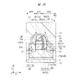
- FIG. 10 is a main-portion cross-sectional view of the semiconductor device of Example 3;
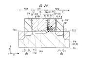
- FIG. 10 is a cross-sectional view of main parts of a semiconductor device according to Example 4.
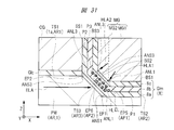
- FIG. 10 is a main part sectional view of a semiconductor device according to Example 5;
- the constituent elements are not necessarily indispensable unless otherwise specified and apparently essential in principle. Needless to say.
- the shapes, positional relationships, etc. of the components, etc. when referring to the shapes, positional relationships, etc. of the components, etc., the shapes are substantially the same unless otherwise specified, or otherwise apparent in principle. And the like are included. The same applies to the above numerical values and ranges.
- hatching may be omitted even in a cross-sectional view for easy viewing of the drawings.
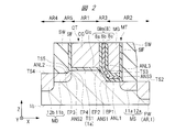
- FIG. 1 to 4 are cross-sectional views of main parts of the semiconductor device according to the embodiment.
- 2 to 4 are enlarged views of a region RG1 surrounded by a two-dot chain line in the cross-sectional view shown in FIG. 2 to 4, illustration of the n ⁇ type semiconductor region VMG, the metal silicide layer 13, the insulating film 14, and the interlayer insulating film 15 is omitted.
- two directions intersecting each other, preferably orthogonal, in the main surface 1 a of the semiconductor substrate 1 are defined as an X-axis direction and a Y-axis direction, and are perpendicular to the main surface 1 a of the semiconductor substrate 1.
- the direction, that is, the vertical direction is defined as the Z-axis direction.
- the term “when viewed from a direction perpendicular to the main surface 1 a of the semiconductor substrate 1” is meant.
- the semiconductor device has a semiconductor substrate 1.
- the semiconductor substrate 1 is a semiconductor wafer made of p-type single crystal silicon having a specific resistance of, for example, about 1 to 10 ⁇ cm.
- the semiconductor substrate 1 has a main surface 1a and a main surface 1b opposite to the main surface 1a.
- the semiconductor substrate 1 has an active region AR as a region on the main surface 1a side.
- the active region AR is defined, that is, partitioned by an element isolation region (not shown), and is electrically isolated from other active regions by this element isolation region.
- a p-type well PW is formed in the active region AR.
- the p-type well PW has a p-type conductivity type.
- a memory cell MC including a memory transistor MT and a control transistor CT is formed in the p-type well PW.
- a plurality of memory cells MC are formed in an array.
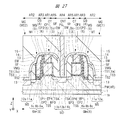
- FIG. 27 described later shows a cross section of two memory cells MC.
- the memory cell MC is a split gate type memory cell. That is, as shown in FIG. 1, the memory cell MC includes a control transistor CT having a control gate electrode CG, and a memory transistor MT connected to the control transistor CT and having a memory gate electrode MG.
- the memory cell MC includes an n-type semiconductor region MS, an n-type semiconductor region MD, a control gate electrode CG, and a memory gate electrode MG.
- the n-type semiconductor region MS and the n-type semiconductor region MD have an n-type conductivity type that is a conductivity type opposite to the p-type conductivity type.
- the control gate electrode CG is formed on the main surface 1 a of the semiconductor substrate 1, and the memory gate electrode MG is formed on the semiconductor substrate 1.
- the memory cell MC has cap insulating films CP1 and CP2 formed over the control gate electrode CG.
- the memory cell MC includes a gate insulating film GIc formed between the control gate electrode CG and the semiconductor substrate 1, between the memory gate electrode MG and the semiconductor substrate 1, and between the memory gate electrode MG and the control gate electrode. And a gate insulating film GIm formed between the CG and the CG.
- the control gate electrode CG and the memory gate electrode MG extend along the main surface 1a of the semiconductor substrate 1 in a state where the gate insulating film GIm is interposed between the opposing side surfaces, that is, the side walls, and are arranged side by side. Has been.
- the extending direction of the control gate electrode CG and the memory gate electrode MG is a direction perpendicular to the paper surface of FIG. 1 (Y-axis direction of FIG. 1).
- the control gate electrode CG is formed on the portion of the p-type well PW located between the semiconductor region MD and the semiconductor region MS, that is, on the semiconductor substrate 1 via the gate insulating film GIc.
- the memory gate electrode MG is formed on the p-type well PW located between the semiconductor region MD and the semiconductor region MS, that is, on the semiconductor substrate 1 via the gate insulating film GIm. Further, the memory gate electrode MG is disposed on the semiconductor region MS side, and the control gate electrode CG is disposed on the semiconductor region MD side.
- the control gate electrode CG, the gate insulating film GIc, the memory gate electrode MG, and the gate insulating film GIm form a memory cell MC, that is, a memory as a nonvolatile memory.
- the control gate electrode CG and the memory gate electrode MG are adjacent to each other with the gate insulating film GIm interposed therebetween.
- the memory gate electrode MG is formed on the side surface of the control gate electrode CG, that is, on the side wall. It is formed in a side wall spacer shape through GIm.
- the gate insulating film GIm is formed between the memory gate electrode MG and the semiconductor substrate 1, that is, the p-type well PW, and between the memory gate electrode MG and the control gate electrode CG.
- the gate insulating film GIc formed between the control gate electrode CG and the p-type well PW functions as a gate insulating film of the control transistor CT. Further, the gate insulating film GIm formed between the memory gate electrode MG and the p-type well PW functions as a gate insulating film of the memory transistor MT.
- the memory gate electrode MG is formed on the side surface of the control gate electrode CG, that is, on the side wall.
- the memory gate electrode MG is formed on the side surface of the control gate electrode CG, that is, the side wall.
- the memory gate electrode MG is formed on the side surface of the control gate electrode CG, that the memory gate electrode MG is formed in contact with the side surface of the control gate electrode CG, or This means that the memory gate electrode MG is formed on the opposite side of the control gate electrode CG across the side surface of the control gate electrode CG.
- the gate insulating film GIc is made of the insulating film 3.
- the insulating film 3 is made of a silicon oxide film, a silicon nitride film or a silicon oxynitride film, or a high dielectric constant film having a higher relative dielectric constant than the silicon nitride film, that is, a so-called High-k film.
- a high-k film or a high dielectric constant film means a film having a higher dielectric constant (relative dielectric constant) than silicon nitride.
- a metal oxide film such as a hafnium oxide film, a zirconium oxide film, an aluminum oxide film, a tantalum oxide film, or a lanthanum oxide film can be used.
- the gate insulating film GIm is made of the insulating film 8.
- the insulating film 8 is composed of a laminated film including, for example, a silicon oxide film 8a, a silicon nitride film 8b as a charge storage portion on the silicon oxide film 8a, and a silicon oxide film 8c on the silicon nitride film 8b.
- the gate insulating film GIm between the memory gate electrode MG and the p-type well PW functions as the gate insulating film of the memory transistor MT as described above.
- the gate insulating film GIm between the memory gate electrode MG and the control gate electrode CG functions as an insulating film for insulating, that is, electrically separating, the memory gate electrode MG and the control gate electrode CG.
- the silicon nitride film 8b is an insulating film for accumulating charges and functions as a charge accumulating portion. That is, the silicon nitride film 8 b is a trapping insulating film formed in the insulating film 8. Therefore, the insulating film 8 can be regarded as an insulating film having a charge storage portion therein.
- the silicon oxide film 8c and the silicon oxide film 8a located above and below the silicon nitride film 8b can function as a charge blocking layer for confining charges.
- charge can be accumulated in the silicon nitride film 8b.
- the silicon oxide film 8a, the silicon nitride film 8b, and the silicon oxide film 8c can also be regarded as ONO (Oxide-Nitride-Oxide) films.
- the control gate electrode CG is made of the conductive film 4.
- the conductive film 4 is made of silicon, for example, an n-type polysilicon film which is a polycrystalline silicon film into which an n-type impurity is introduced.
- the control gate electrode CG is made of a patterned conductive film 4.
- the memory gate electrode MG is made of a conductive film 9.
- the conductive film 9 is made of silicon, for example, an n-type polysilicon film which is a polycrystalline silicon film into which an n-type impurity is introduced.
- the memory gate electrode MG is formed by anisotropically etching, that is, etching back, the conductive film 9 formed on the semiconductor substrate 1 so as to cover the control gate electrode CG, and the insulating film 8 is interposed on the side wall of the control gate electrode CG. It is formed by leaving the conductive film 9. For this reason, the memory gate electrode MG is formed on the side wall of the control gate electrode CG in the shape of a side wall spacer via the insulating film 8.
- the cap insulating film CP1 is made of an insulating film 5 containing silicon and oxygen
- the cap insulating film CP2 is made of an insulating film 6 containing silicon and nitrogen.
- the cap insulating films CP1 and CP2 are protective films that protect the control gate electrode CG, and are hard mask films when the conductive film 4 is patterned to form the control gate electrode CG.
- the cap insulating films CP1 and CP2 are cap films for adjusting the height of each upper surface of the memory gate electrode MG when the conductive film 9 is etched back to form the memory gate electrode MG.
- the length of the cap insulating film CP2 in the X-axis direction may be shorter than the length of the control gate electrode CG in the X-axis direction, ie, the gate length direction.
- the gate length of the control gate electrode CG intersects the direction in which the control gate electrode CG extends (Y-axis direction in FIG. 1), preferably orthogonally cross (X-axis in FIG. 1). (Direction) means the length of the control gate electrode CG.
- the semiconductor region MS is a semiconductor region that functions as one of a source region or a drain region
- the semiconductor region MD is a semiconductor region that functions as the other of a source region or a drain region
- the semiconductor region MS is a semiconductor region that functions as a source region, for example
- the semiconductor region MD is a semiconductor region that functions as a drain region, for example.
- Each of the semiconductor regions MS and MD is composed of a semiconductor region into which an n-type impurity is introduced and has an LDD (Lightly doped drain) structure.
- the source semiconductor region MS includes an n ⁇ type semiconductor region 11a and an n + type semiconductor region 12a having an impurity concentration higher than that of the n ⁇ type semiconductor region 11a.
- the drain semiconductor region MD includes an n ⁇ type semiconductor region 11b and an n + type semiconductor region 12b having an impurity concentration higher than that of the n ⁇ type semiconductor region 11b.
- the n + type semiconductor region 12a has a deeper junction depth and a higher impurity concentration than the n ⁇ type semiconductor region 11a, and the n + type semiconductor region 12b has a junction depth higher than that of the n ⁇ type semiconductor region 11b. Is deep and the impurity concentration is high.
- a side wall spacer SW made of an insulating film such as a silicon oxide film, a silicon nitride film, or a laminated film thereof is formed. Sidewall spacers SW are formed in portions adjacent to the control gate electrode CG on the opposite side of the memory gate electrode MG across the control gate electrode CG. A side wall spacer SW is formed in a portion adjacent to the memory gate electrode MG on the opposite side of the control gate electrode CG across the memory gate electrode MG.
- an insulating film SIF made of, for example, silicon oxide is interposed between the control gate electrode CG and the sidewall spacer SW and between the memory gate electrode MG and the sidewall spacer SW. It may be.
- the n ⁇ type semiconductor region 11a is formed in a self-aligned manner with respect to the side surface of the memory gate electrode MG, and the n + type semiconductor region 12a is self-aligned with respect to the side surface of the sidewall spacer SW on the side surface of the memory gate electrode MG. It is formed consistently. For this reason, the low concentration n ⁇ type semiconductor region 11a is formed under the sidewall spacer SW on the side surface of the memory gate electrode MG, and the high concentration n + type semiconductor region 12a is a low concentration n ⁇ type semiconductor region. It is formed outside the region 11a. Therefore, the high concentration n + type semiconductor region 12a is formed so as to be in contact with the low concentration n ⁇ type semiconductor region 11a.
- the n ⁇ type semiconductor region 11b is formed in a self-aligned manner with respect to the side surface of the control gate electrode CG, and the n + type semiconductor region 12b is self-aligned with respect to the side surface of the sidewall spacer SW on the side surface of the control gate electrode CG. It is formed consistently. Therefore, the low concentration n ⁇ type semiconductor region 11b is formed under the sidewall spacer SW on the side surface of the control gate electrode CG, and the high concentration n + type semiconductor region 12b is a low concentration n ⁇ type semiconductor region. It is formed outside the region 11b. Therefore, the high concentration n + type semiconductor region 12b is formed so as to be in contact with the low concentration n ⁇ type semiconductor region 11b. As will be described later with reference to FIG. 27, two adjacent memory cells MC share a high concentration n + type semiconductor region 12b.
- a channel region of the control transistor CT is formed in the upper layer portion of the p-type well PW located below the gate insulating film GIc below the control gate electrode CG.
- n ⁇ type semiconductor region VMG is formed in the upper layer portion of the portion of the p-type well PW located below the gate insulating film GIm below the memory gate electrode MG.
- the n ⁇ type semiconductor region VMG is for adjusting the threshold voltage Vth of the memory transistor MT, and is formed so as to be in contact with the n ⁇ type semiconductor region 11a.
- the n-type impurity concentration in the n ⁇ -type semiconductor region VMG is lower than the n-type impurity concentration in the n ⁇ -type semiconductor region 11a.
- a metal silicide layer 13 is formed on each of the n + -type semiconductor regions 12a and 12b, that is, each of the upper surface of the n + -type semiconductor regions 12a and 12b, a salicide (Salicide: Self Aligned Silicide) technique or the like.
- the metal silicide layer 13 is made of, for example, a cobalt silicide layer, a nickel silicide layer, or a platinum-added nickel silicide layer.
- the metal silicide layer 13 can reduce diffusion resistance and contact resistance.
- the metal silicide layer 13 may be formed on the memory gate electrode MG.
- An insulating film 14 is formed on the semiconductor substrate 1 so as to cover the control gate electrode CG, the cap insulating film CP2, the memory gate electrode MG, and each sidewall spacer SW.
- the insulating film 14 is made of, for example, a silicon nitride film.
- An interlayer insulating film 15 is formed on the insulating film 14.
- the interlayer insulating film 15 is made of a single film of a silicon oxide film or a laminated film of a silicon nitride film and a silicon oxide film.
- the upper surface of the interlayer insulating film 15 is planarized.
- a contact hole CNT may be formed in the interlayer insulating film 15, and a conductive plug PG may be embedded as a conductor portion in the contact hole CNT.
- the active region AR as the region on the main surface 1a side includes the regions AR1 to AR3. That is, the semiconductor substrate 1 includes regions AR1 to AR3 as regions on the main surface 1a side.
- the region AR2 is disposed on the positive side in the X-axis direction with respect to the region AR1 in plan view, and is adjacent to the region AR1, and the region AR3 is disposed between the region AR1 and the region AR2.
- the control gate electrode CG is formed on the upper surface TS1 of the region AR1.
- the memory gate electrode MG and the sidewall spacer SW on the side surface of the memory gate electrode MG are formed on the upper surface TS2 of the region AR2.
- the gate insulating film GIm is formed between the memory gate electrode MG and the control gate electrode CG, and between the memory gate electrode MG and the upper surface TS2.
- the n ⁇ type semiconductor region 11a and the n + type semiconductor region 12a are formed in the upper layer portion of the region AR2.
- the upper surface TS2 of the area AR2 is lower than the upper surface TS1 of the area AR1. That is, the upper surface TS2 of the region AR2 is disposed on the main surface 1b side with respect to the upper surface TS1 of the region AR1 in the Z-axis direction.
- the region AR3 has a connection surface TS3 that connects the upper surface TS1 of the region AR1 and the upper surface TS2 of the region AR2.
- the gate insulating film GIm is also formed between the memory gate electrode MG and the connection surface TS3. That is, the gate insulating film GIm is formed on the connection surface TS3 and the upper surface TS2.
- the end portion EP1 of the connection surface TS3 is connected to the upper surface TS2 of the region AR2, and the end portion EP2 opposite to the end portion EP1 of the connection surface TS3 is connected to the upper surface TS1 of the region AR1.
- the end portion EP1 of the connection surface TS3 is arranged on the positive side in the X-axis direction with respect to the end portion EP2 of the connection surface TS3 in the X-axis direction, and is below the end portion EP2 of the connection surface TS3, that is, In the Z-axis direction, it is arranged on the main surface 1b side with respect to the end portion EP2.
- connection surface TS3 has the upper surface TS2 such that the end portion EP1 is located on the positive side in the X-axis direction with respect to the end portion EP2 and is located below the end portion EP2 in the Z-axis direction.
- the YZ plane ie, the plane perpendicular to the X-axis direction.
- the upper surface TS1 of the region AR1 is the same surface as the main surface 1a of the semiconductor substrate 1.
- the active area AR as the area on the main surface 1a side includes areas AR4 and AR5. That is, semiconductor substrate 1 includes regions AR4 and AR5 as regions on the main surface 1a side.
- the area AR4 is arranged on the negative side in the X-axis direction, that is, on the opposite side to the positive side in the X-axis direction with respect to the area AR1 in plan view, and is adjacent to the area AR1, and the area AR5 is the area AR1. It arrange
- the sidewall spacer SW on the side surface of the control gate electrode CG is formed on the upper surface TS4 of the region AR4.
- the n ⁇ type semiconductor region 11b and the n + type semiconductor region 12b are formed in the upper layer portion of the region AR4.
- the upper surface TS4 of the region AR4 is lower than the upper surface TS1 of the region AR1. That is, the upper surface TS4 of the region AR4 is arranged on the main surface 1b side with respect to the upper surface TS1 of the region AR1 in the Z-axis direction.
- the region AR5 has a connection surface TS5 that connects the upper surface TS1 of the region AR1 and the upper surface TS4 of the region AR4.
- the end portion EP3 of the connection surface TS5 is connected to the upper surface TS4 of the region AR4, and the end portion EP4 opposite to the end portion EP3 of the connection surface TS5 is connected to the upper surface TS1 of the region AR1.
- the end portion EP3 of the connection surface TS5 is disposed on the negative side in the X-axis direction with respect to the end portion EP4 of the connection surface TS5, and is lower than the end portion EP4 of the connection surface TS5, that is, in the Z-axis direction. It arrange
- connection surface TS5 has an upper surface TS4 such that the end portion EP3 is located on the negative side in the X-axis direction with respect to the end portion EP4 and is located below the end portion EP4 in the Z-axis direction. It is inclined with respect to both the YZ plane and the YZ plane.
- the upper surface TS2 of the region AR2 is lower than the upper surface TS4 of the region AR4. That is, the upper surface TS2 of the region AR2 is arranged on the main surface 1b side with respect to the upper surface TS4 of the region AR4 in the Z-axis direction.
- the upper surface TS4 of the region AR4 can be disposed at almost the same height as the upper surface TS1 of the region AR1. Therefore, the distribution of the n ⁇ -type semiconductor region 11b and the n + -type semiconductor region 12b is hardly changed compared to the case where the upper surface TS4 of the region AR4 is arranged at the same height as the upper surface TS1 of the region AR1. It is possible to prevent or suppress a decrease in flowing on-current.
- an angle formed by the connection surface TS3 and the upper surface TS2 is defined as an angle ANS1 as an acute angle.
- an obtuse angle between the connection surface TS3 and the upper surface TS2 is represented by an angle ANL1.
- the sum of the angle ANS1 and the angle ANL1 is equal to 180 °.
- the angle ANS1 is greater than 0 ° and less than 90 °. In other words, the angle ANL1 is less than 180 ° and greater than 90 °.
- connection surface TS5 and the upper surface TS4 an angle formed by the connection surface TS5 and the upper surface TS4 is defined as an angle ANS2 as an acute angle.
- an obtuse angle between the connection surface TS5 and the upper surface TS4 is represented by an angle ANL2.
- the sum of the angle ANS2 and the angle ANL2 is equal to 180 °.
- an acute angle ANS1 formed by the connection surface TS3 and the upper surface TS2 is larger than an acute angle ANS2 formed by the connection surface TS5 and the upper surface TS4.
- This also makes it possible to arrange the upper surface TS4 of the region AR4 at almost the same height as the upper surface TS1 of the region AR1. Therefore, the distribution of the n ⁇ -type semiconductor region 11b and the n + -type semiconductor region 12b is hardly changed compared to the case where the upper surface TS4 of the region AR4 is arranged at the same height as the upper surface TS1 of the region AR1. It is possible to prevent or suppress a decrease in flowing on-current.
- connection surface TS3 no corner is formed between the portion on the upper surface TS2 side of the connection surface TS3 and the portion on the connection surface TS3 side of the upper surface TS2, and the portion on the upper surface TS2 side of the connection surface TS3, and The portion on the connection surface TS3 side of the upper surface TS2 may form the same curved surface.
- a virtual plane TS31 formed by extending a portion of the connection surface TS3 on the upper surface TS1 side as the same plane to the upper surface TS2 side is opposite to the connection surface TS3 side of the upper surface TS2.
- An angle formed with a virtual plane TS21 formed by extending the portion as the same plane toward the connection surface TS3 is defined as an angle ANS1 as an acute angle.
- the angle ANL1 is an obtuse angle between the plane TS31 and the plane TS21, and is an angle such that the sum of the angle ANS1 and the angle ANL1 is equal to 180 °.
- the end portion EP11 opposite to the end portion EP2 of the plane TS31 is connected to the plane TS21.
- a corner is not formed between the portion of the connection surface TS5 on the upper surface TS4 side and the portion of the upper surface TS4 on the connection surface TS5 side, and the portion of the connection surface TS5 on the upper surface TS4 side.
- the portion of the upper surface TS4 on the connection surface TS5 side forms the same curved surface.
- a virtual plane formed by extending the portion on the upper surface TS1 side of the connection surface TS5 to the upper surface TS4 side as the same plane is the upper surface TS4.
- An angle formed with a virtual plane formed by extending the portion opposite to the connection surface TS5 side to the connection surface TS5 side as the same plane can be defined as an angle ANS2 as an acute angle.
- the angle ANL2 is an obtuse angle between the respective virtual planes, and is an angle such that the sum of the angle ANS2 and the angle ANL2 is equal to 180 °.
- the memory gate electrode MG includes an electrode part MG1 formed on the upper surface TS2, and an electrode part MG2 formed on the control gate electrode CG side with respect to the electrode part MG1.
- the electrode portion MG2 has a connection surface BS2 as a lower surface that connects the lower surface BS1 of the electrode portion MG1 and the side surface BS3 of the electrode portion MG2 on the control gate electrode CG side. As shown in FIG.
- the end portion EP5 of the connection surface BS2 of the electrode portion MG2 is connected to the lower surface BS1 of the electrode portion MG1, and the end portion EP6 opposite to the end portion EP5 of the connection surface BS2 of the electrode portion MG2 is It is connected to the side surface BS3 of the electrode part MG2.
- the end portion EP5 is disposed on the positive side in the X-axis direction with respect to the end portion EP6, and is disposed below the end portion EP6 in the Z-axis direction.
- corner AP1 is formed by the lower surface BS1 and the connection surface BS2
- corner AP2 is formed by the connection surface BS2 and the side surface BS3.
- a corner is not formed between the portion on the lower surface BS1 side of the connection surface BS2 and the portion on the connection surface BS2 side of the lower surface BS1, and a portion on the lower surface BS1 side of the connection surface BS2;
- the portion of the lower surface BS1 on the connection surface BS2 side may form the same curved surface.
- the virtual plane BS21 formed by extending the side surface BS3 side portion of the connection surface BS2 to the lower surface BS1 side as the same plane is the same as the portion of the lower surface BS1 opposite to the connection surface BS2 side.
- An angle formed with a virtual plane BS11 formed by extending the connection plane BS2 as a plane can be defined as an angle ANS1 as an acute angle.
- the angle ANL1 is an obtuse angle between the plane BS21 and the plane BS11, and is an angle such that the sum of the angle ANS1 and the angle ANL1 is equal to 180 °.
- an end EP51 opposite to the end EP6 of the plane BS21 is connected to the plane BS11.
- a region RG2 surrounded by a two-dot chain line is enlarged.
- injection of electrons into the silicon nitride film 8b, which is a charge storage portion in the insulating film 8 of the memory transistor, is defined as “writing”, and injection of holes, that is, holes, is defined as “erasing”. To do. Further, the power supply voltage Vdd is set to 1.5V.
- the writing method hot electron writing called a source side injection (SSI) method can be used.
- the voltage Vd applied to the semiconductor region MD is, for example, about the power supply voltage Vdd
- the voltage Vcg applied to the control gate electrode CG is, for example, about 1 V
- the voltage Vmg applied to the memory gate electrode MG is For example, it is about 12V.
- the voltage Vs applied to the semiconductor region MS is set to about 6 V, for example
- the voltage Vb applied to the p-type well PW is set to about 0 V, for example. Then, each voltage described above is applied to each part of the memory cell MC to be written.
- an electron EL is injected into the silicon nitride film 8b in the gate insulating film GIm of the memory cell MC, and data is written into the memory cell MC.
- Hot electrons are generated mainly in a channel region located below the memory gate electrode MG via the gate insulating film GIm, and injected into the silicon nitride film 8b which is a charge storage portion in the gate insulating film GIm.
- the injected hot electrons are captured by the trap level in the silicon nitride film 8b in the gate insulating film GIm, and as a result, the threshold voltage of the memory transistor increases.
- a method of injecting holes as hot holes by band-to-band tunneling (BTBT) phenomenon can be used for erasing, but direct tunneling phenomenon, that is, Fowler Nordheim (Fowler) It is preferable to use an erasing method by hole injection utilizing the -Nordheim: FN) type tunnel phenomenon.
- FN -Nordheim
- erasing is performed by injecting holes into the charge storage portion, that is, the silicon nitride film 8b in the gate insulating film GIm by the direct tunnel phenomenon.
- the voltage Vd is, for example, about 0 V
- the voltage Vcg is, for example, about 0 V
- the voltage Vmg is, for example, about 12 V
- the voltage Vs is, for example, about 0 V
- the voltage Vb is, for example, about 0 V.
- holes HL are injected from the memory gate electrode MG side into the charge storage portion, that is, the silicon nitride film 8b by the direct tunneling phenomenon through the silicon oxide film 8c. Erasing is performed by canceling out the electrons in the film 8b. Alternatively, erasing is performed by the holes injected into the silicon nitride film 8b being captured by trap levels in the silicon nitride film 8b. As a result, the threshold voltage of the memory transistor is lowered and the memory transistor enters an erased state.
- the voltage Vd is, for example, about the power supply voltage Vdd
- the voltage Vcg is, for example, about the power supply voltage Vdd
- the voltage Vmg is, for example, about 0 V
- the voltage Vs is, for example, about 0,
- the voltage Vb is, for example, about 0 V.
- Each voltage described above is applied to each part of the memory cell MC to be read.
- 5 and 6 are process flowcharts showing a part of the manufacturing process of the semiconductor device of the embodiment.
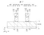
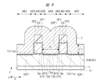
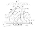
- 7 to 27 are fragmentary cross-sectional views of the semiconductor device of the embodiment during the manufacturing process.
- FIG. 7 to 27 are sectional views showing manufacturing steps for forming the memory cells MC1 and MC2 as the two memory cells MC shown in FIG.
- the arrangement of the memory cell MC1 is the same as the arrangement of the memory cell MC shown in FIG. 1, but the arrangement of the memory cell MC2 is opposite to the arrangement of the memory cell MC1.
- Arrangement. That is, the memory cells MC1 and MC2 are arranged symmetrically with respect to the YZ plane between the memory cell MC1 and the memory cell MC2.
- a manufacturing process for mainly forming the memory cell MC1 out of the two memory cells MC1 and MC2 will be described.
- a semiconductor substrate 1 is prepared as a semiconductor wafer made of p-type single crystal silicon having a specific resistance of about 1 to 10 ⁇ cm, for example (step S1 in FIG. 5).
- the semiconductor substrate 1 has a main surface 1a and a main surface 1b opposite to the main surface 1a.
- the semiconductor substrate 1 has an active region AR as a region on the main surface 1a side.
- the active region AR is defined, that is, partitioned by an element isolation region (not shown), and is electrically isolated from other active regions by this element isolation region.
- a p-type well PW is formed in the active region AR.
- the p-type well PW has a p-type conductivity type.
- the active area AR as the area on the main surface 1a side includes areas AR1 to AR5. That is, in step S1, the semiconductor substrate 1 including the regions AR1 to AR5 as the region on the main surface 1a side is prepared. In the region where the memory cell MC1 (see FIG. 27 described later) is formed, the region AR2 is disposed on the positive side in the X-axis direction with respect to the region AR1 in plan view, and is adjacent to the region AR1. AR3 is arranged between the area AR1 and the area AR2.
- the area AR4 is arranged on the negative side in the X-axis direction, that is, on the opposite side to the positive side in the X-axis direction with respect to the area AR1 in plan view, and is adjacent to the area AR1, and the area AR5 is the area AR1. It arrange
- a p-type well PW is formed in the active region AR (step S2 in FIG. 5).
- the p-type well PW can be formed by introducing a p-type impurity such as boron (B) into the semiconductor substrate 1 by an ion implantation method or the like.
- the p-type well PW is formed from the main surface 1a of the semiconductor substrate 1 to a predetermined depth.
- the natural oxide film on the surface of the semiconductor substrate 1 is removed by, for example, wet etching using a hydrofluoric acid (HF) aqueous solution, and the surface of the semiconductor substrate 1 is cleaned to clean the surface of the semiconductor substrate 1. .
- HF hydrofluoric acid
- the insulating film 3, the conductive film 4, and the insulating films 5 and 6 are formed over the entire main surface 1a of the semiconductor substrate 1 (step S3 in FIG. 5).
- an insulating film 3 is formed on the main surface 1a of the semiconductor substrate 1 as shown in FIG.
- a silicon oxide film, a silicon nitride film or a silicon oxynitride film, or a high-k film, that is, a high dielectric constant film can be used as the insulating film 3, and examples of materials that can be used as the insulating film 3 are as follows.
- the insulating film 3 can be formed using a thermal oxidation method, a sputtering method, an atomic layer deposition (ALD) method, a chemical vapor deposition (CVD) method, or the like.
- a conductive film 4 is formed on the entire main surface 1a of the semiconductor substrate 1, that is, on the insulating film 3.
- the conductive film 4 is made of a polycrystalline silicon film, that is, a silicon film such as a polysilicon film.
- a conductive film 4 can be formed using a CVD method or the like.
- the film thickness of the conductive film 4 can be set to a sufficient thickness so as to cover the insulating film 3.
- the conductive film 4 can be formed as an amorphous silicon film during film formation, and the amorphous silicon film can be converted into a polycrystalline silicon film by subsequent heat treatment.
- a conductive film 4 having a low resistivity by introducing an n-type impurity such as phosphorus (P) or arsenic (As) or a p-type impurity such as boron (B). Impurities can be introduced during or after the formation of the conductive film 4.
- the conductive film 4 into which the impurities are introduced can be formed by adding a doping gas to the gas for forming the conductive film 4.
- the conductive film 4 into which impurities are introduced can be formed.
- an insulating film 5 is formed on the entire main surface 1a of the semiconductor substrate 1, that is, on the conductive film 4.
- the insulating film 5 made of a silicon oxide film can be formed by thermally oxidizing the surface of the conductive film 4 made of a silicon film.
- the insulating film 5 made of a silicon oxide film can be formed using a CVD method.
- the material of the insulating film 5 an insulating film made of other materials can be used instead of the silicon oxide film.
- the insulating film 6 can be formed directly on the conductive film 4 without forming the insulating film 5.
- an insulating film 6 containing silicon and nitrogen is formed on the entire main surface 1a of the semiconductor substrate 1, that is, on the insulating film 5.
- the insulating film 6 made of a silicon nitride film can be formed using, for example, a CVD method.
- step S4 the insulating films 6 and 5 and the conductive film 4 are patterned (step S4 in FIG. 5).
- the insulating films 6 and 5 and the conductive film 4 are patterned using, for example, photolithography and etching.
- a resist film (not shown) is formed on the insulating film 6.
- an opening that penetrates the resist film and reaches the insulating film 6 is formed in a region other than the region where the control gate electrode CG is to be formed, and a resist pattern (not shown) is made of the resist film in which the opening is formed. ).
- the portion of the insulating film 6 disposed in the region where the control gate electrode CG is to be formed is covered with a resist film.
- the insulating films 6 and 5 and the conductive film 4 are etched and patterned by, for example, dry etching.
- control gate electrode CG made of the conductive film 4 is formed on the main surface 1 a of the semiconductor substrate 1, and between the control gate electrode CG and the semiconductor substrate 1, between the control gate electrode CG and the semiconductor substrate 1.
- a gate insulating film GIc made of the insulating film 3 is formed. Specifically, the control gate electrode CG is formed on the upper surface TS1 of the region AR1.
- the portion of the insulating film 3 that is not covered with the control gate electrode CG can be removed by performing dry etching in step S4 or by performing wet etching after the dry etching in step S4. Then, in the portion where the control gate electrode CG is not formed, the p-type well PW of the semiconductor substrate 1 is exposed.
- a sacrificial oxide film SOF1 is formed (step S5 in FIG. 5).
- the main surface 1a of the semiconductor substrate 1 and the side surfaces of the control gate electrode CG are oxidized to form a sacrificial oxide film SOF1.
- the sacrificial oxide film SOF1 is an etching stopper film when the film 7 is etched.
- the sacrificial oxide film SOF1 can be formed by, for example, a thermal oxidation method or an ISSG (In Situ Steam Generation) oxidation method, or by using a combination of a thermal oxidation method and an ISSG oxidation method.
- the upper surface TS4 of the region AR4 is made lower than the upper surface TS1 of the region AR1 by oxidizing the surface of the region AR4. Then, a connection surface TS5 that connects the upper surface TS1 of the region AR1 and the upper surface TS4 of the region AR4 is formed in the region AR5 arranged between the region AR1 and the region AR4.
- the sacrificial oxide film SOF1 When the sacrificial oxide film SOF1 is formed, oxygen is sufficiently supplied at the time of oxidation in a region where there is no pattern such as the region AR4, that is, in a region away from the control gate electrode CG, the surface of the region AR4 Is oxidized with a substantially constant thickness.
- the region AR5 adjacent to the pattern of the control gate electrode CG since the pattern of the control gate electrode CG exists on the semiconductor substrate 1, the closer to the control gate electrode CG, the more the oxide is compared with the case where there is no pattern nearby. The supply of oxygen at the time decreases, and therefore the progress of oxidation is delayed. Accordingly, in the region AR5, the connection surface TS5 that is inclined from the end on the region AR4 side to the end on the control gate electrode CG side is formed.
- the end portion EP3 of the connection surface TS5 is connected to the upper surface TS4 of the region AR4, and the end portion EP4 opposite to the end portion EP3 of the connection surface TS5 is connected to the upper surface TS1 of the region AR1. Further, the end portion EP3 of the connection surface TS5 is disposed on the opposite side to the region AR2 side in the X-axis direction with respect to the end portion EP4 of the connection surface TS5, and the end portion EP4 of the connection surface TS5 in the Z-axis direction. It is arranged below.
- connection surface TS5 the end portion EP3 is located on the opposite side to the region AR2 side in the X-axis direction with respect to the end portion EP4, and is located below the end portion EP4 in the Z-axis direction.
- it inclines with respect to both upper surface TS4 and YZ plane.
- a film 7 is formed on the semiconductor substrate 1 so as to cover the control gate electrode CG (step S6 in FIG. 5).
- the sacrificial oxide film SOF1 is an etching stopper film when the film 7 is etched.
- the film 7 is made of, for example, a polycrystalline silicon film, that is, a silicon film such as a polysilicon film.
- a film 7 can be formed using a CVD method or the like.
- the film 7 may be formed as an amorphous silicon film at the time of film formation, and the amorphous silicon film may be converted into a polycrystalline silicon film by subsequent heat treatment.
- the film 7 is formed between the two adjacent control gate electrodes CG even when the film 7 is etched back by the thickness of the film 7. It is preferable that the film thickness be embedded. Therefore, it is preferable that the film thickness FT1 of the film 7 is, for example, one half or more of the interval IT1 between the side surfaces facing each other of the adjacent control gate electrodes CG.
- the film 7 is etched back using an anisotropic etching technique to form a spacer SP11 as a side wall (step S7 in FIG. 5).
- the film 7 is etched back by the thickness of the film 7, thereby leaving the film 7 in the shape of a sidewall spacer on both side surfaces of the control gate electrode CG via the sacrificial oxide film SOF1, for example.
- the film 7 is placed on the side wall spacer on the side surface opposite to the side where the memory gate electrode MG (see FIG. 19 described later) adjacent to the control gate electrode CG is disposed, on both side surfaces of the control gate electrode CG.
- a spacer SP11 made of the remaining film 7 is formed.
- a memory gate electrode MG adjacent to the one control gate electrode CG is disposed on the opposite side of the other control gate electrode CG across the one control gate electrode CG.
- the film 7 is buried between the two adjacent control gate electrodes CG.
- each of the two side surfaces of the two adjacent control gate electrodes CG is formed on the side surface opposite to the side where the memory gate electrode MG adjacent to the control gate electrode CG is disposed.
- the two spacers SP11 are arranged without being spaced from each other. That is, the two spacers SP11 are integrally formed.
- the remaining film 7 A spacer SP12 made of is formed.
- step S8 in FIG. 5 the spacer SP12 is removed.
- a resist pattern R1 that covers the spacer SP11 and exposes the spacer SP12 is formed on the semiconductor substrate using photolithography.
- a resist film RF1 as a mask film is formed on the sacrificial oxide film SOF1, that is, on the semiconductor substrate 1, so as to cover the spacers SP11 and SP12.
- the resist film RF1 is patterned to form a resist pattern R1 as a mask pattern made of the resist film RF1 covering the spacer SP11, and the spacer SP12 is exposed from the resist film RF1.
- the spacer SP12 is removed by dry etching using the formed resist pattern R1 as an etching mask.
- the spacer SP11 is covered with the resist pattern R1, it remains without being etched.
- step S8 the resist pattern R1 is thereafter removed as shown in FIG.
- step S9 the sacrificial oxide film SOF1 is removed (step S9 in FIG. 5).
- step S9 the sacrificial oxide film SOF1 exposed from the control gate electrode CG and the spacer SP11 is removed by etching, for example, by dry etching. Thereby, the main surface 1a of the semiconductor substrate 1 is exposed in the regions AR2 and AR3.
- step S10 the surface of the semiconductor substrate 1 is etched (step S10 in FIG. 5).
- the surface of each of the regions AR2 and AR3 in the semiconductor substrate 1 is etched by dry etching using the control gate electrode CG, the cap insulating film CP2 on the control gate electrode CG, and the spacer SP11 as an etching mask. To do.
- the upper surface TS2 of the region AR2 is made lower than the upper surface TS1 of the region AR1, and the upper surface TS1 of the region AR1 and the upper surface TS2 of the region AR2 are arranged in the region AR3 arranged between the region AR1 and the region AR2.
- a connection surface TS3 to be connected is formed. Note that the upper surface TS2 of the region AR2 is set lower than the upper surface TS4 of the region AR4.
- connection surface TS3 is connected to the upper surface TS2 of the region AR2, and the end portion EP2 opposite to the end portion EP1 of the connection surface TS3 is connected to the upper surface TS1 of the region AR1. Further, the end portion EP1 of the connection surface TS3 is disposed on the opposite side to the region AR4 side in the X-axis direction with respect to the end portion EP2 of the connection surface TS3, and the end portion EP2 of the connection surface TS3 in the Z-axis direction. It is arranged below.
- connection surface TS3 the end portion EP1 is located on the opposite side to the region AR4 side in the X-axis direction with respect to the end portion EP2, and is located below the end portion EP2 in the Z-axis direction.
- it inclines with respect to both upper surface TS2 and YZ plane.
- the etching conditions in this step S10 are the selection ratio between the cap insulating film CP2 made of the insulating film 6 such as a silicon nitride film and the semiconductor substrate 1 made of silicon, for example, the etching rate of the cap insulating film CP2. It is desirable that the ratio of the etching rate of the semiconductor substrate 1 with respect to is as high as possible.
- the step of actually depositing the deposit on the surface and the step of etching the surface are repeated, and the deposit is deposited in an amount to be etched.
- Etching proceeds when the amount exceeds the predetermined amount.
- the amount of deposits is larger than the amount of etching due to the presence of the side surfaces of the control gate electrode CG.
- the connection surface TS3 that is inclined from the end on the control gate electrode CG side to the end on the region AR2 side is formed.
- the inclination angle of the connection surface TS3 can be adjusted within a certain range by changing the balance between the amount of deposits deposited under the etching conditions and the amount etched.
- step S10 since the upper part of the spacer SP11 is slightly etched, the upper surface of the spacer SP11 after performing step S10 is lower than the upper surface of the spacer SP11 before performing step S10.
- the acute angle ANS1 formed by the connection surface TS3 and the upper surface TS2 is larger than the acute angle ANS2 formed by the connection surface TS5 and the upper surface TS4.
- step S11 in FIG. 5 the spacer SP11 is removed.
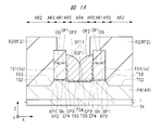
- step S11 first, as shown in FIG. 14, a resist pattern R2 that covers the regions AR2 and AR3 and exposes the spacer SP11 is formed on the semiconductor substrate 1 using photolithography.
- a resist film RF2 as a mask film is formed on the semiconductor substrate 1 so as to cover the spacer SP11.
- the resist film RF2 is patterned to form a resist pattern R2 made of a resist film RF2 covering the regions AR2 and AR3, and the spacer SP11 is exposed from the resist film RF2.
- step S11 next, as shown in FIG. 15, the spacer SP11 is removed by dry etching using the formed resist pattern R2 as an etching mask. On the other hand, since the regions AR2 and AR3 are covered with the resist pattern R2, they are left without being etched.
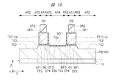
- an n ⁇ type semiconductor region VMG is formed (step S12 in FIG. 6).
- the side surface of the main surface 1a of the semiconductor substrate 1 and the side surface of the control gate electrode CG on the side where the sacrificial oxide film SOF1 is not formed is oxidized and sacrificed.
- An oxide film SOF2 is formed.
- the sacrificial oxide film SOF2 can be formed, for example, by a thermal oxidation method or an ISSG oxidation method, or by using a combination of a thermal oxidation method and an ISSG oxidation method.
- the p-type well PW is formed, for example, with the cap insulating film CP2 and the control gate electrode CG having the sacrificial oxide films SOF1 and SOF2 formed on the side surfaces as masks.
- An n-type impurity such as (P) or arsenic (As) is introduced by an ion implantation method.
- the upper portion of the p-type well PW located on the side where the memory gate electrode MG (see FIG. 19 described later) is arranged with respect to the control gate electrode CG, that is, the upper portion of each of the regions AR2 and AR3.
- N ⁇ type semiconductor region VMG is formed.
- the sacrifice is caused on the upper surface of the p-type well PW in the portion located on the side where the memory gate electrode MG (see FIG. 19 described later) adjacent to the control gate electrode CG is arranged.
- An oxide film SOF2 is formed. Therefore, when the n-type impurity is introduced into the p-type well PW by the ion implantation method, it is possible to prevent the upper surface of the p-type well PW from being damaged.
- the upper surface TS2 of the region AR2 is lower than the upper surface TS1 of the region AR1, and the connection surface TS3 that connects the upper surface TS1 and the upper surface TS2 is formed between the upper surface TS1 and the upper surface TS2. Further, the end portion EP1 on the upper surface TS2 side of the connection surface TS3 is disposed on the opposite side to the control gate electrode CG with respect to the end portion EP2 on the upper surface TS1 side of the connection surface TS3, and the end portion EP2 in the Z-axis direction. It is arranged below.
- impurity ions implanted by ion implantation are introduced to the p-type well PW located below the control gate electrode CG across the connection surface TS3, so that the n ⁇ type semiconductor region VMG is formed in a desired region. Can be formed with good shape accuracy.
- the n ⁇ type semiconductor region VMG may be formed on the opposite side of the control gate electrode CG from the side where the memory gate electrode MG adjacent to the control gate electrode CG is disposed.
- the illustration of the n ⁇ type semiconductor region formed on the opposite side of the control gate electrode CG from the side where the memory gate electrode MG adjacent to the control gate electrode CG is arranged is omitted.
- the n ⁇ type semiconductor region VMG is also formed in the upper layer portion of each of the regions AR4 and AR5, but is not shown in FIG.
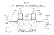
- the cap insulating film CP2 is slimmed (step S13 in FIG. 6).
- the sacrificial oxide films SOF1 and SOF2 and the cap insulating film CP1 are silicon oxide films and the cap insulating film CP2 is a silicon nitride film
- phosphoric acid having a temperature of about 140 to 170 ° C., that is, hot phosphoric acid, for example. Is etched using as an etchant.
- the ratio of the etching rate of the cap insulating film CP2 to the etching rate of the sacrificial oxide films SOF1 and SOF2 and the cap insulating film CP1 that is, the selection ratio can be sufficiently increased, so that the cap insulating film CP2 is selectively etched. can do.
- the length of the cap insulating film CP2 in the X-axis direction, that is, the gate length direction can be made shorter than the length of the control gate electrode CG in the X-axis direction, that is, the gate length direction. That is, the cap insulating film CP2 can be slimmed.
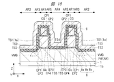
- an insulating film 8 is formed on the entire main surface 1a of the semiconductor substrate 1 (step S14 in FIG. 6).
- the insulating film 8 is formed on the exposed portion of the semiconductor substrate 1, that is, on the upper surface TS2 and the connection surface TS3, and on the surface of the control gate electrode CG and the surface of the cap insulating film CP2. That is, in step S14, the insulating film 8 is formed on the semiconductor substrate 1 so as to cover the control gate electrode CG and the cap insulating film CP2.
- the insulating film 8 is an insulating film having a charge storage portion therein, and is composed of a stacked film of a silicon oxide film 8a, a silicon nitride film 8b, and a silicon oxide film 8c formed in this order from the bottom.
- the silicon oxide film 8a can be formed by, for example, a thermal oxidation method or an ISSG oxidation method.
- the silicon nitride film 8b of the insulating film 8 can be formed by, for example, a CVD method.
- the silicon oxide film 8c of the insulating film 8 can be formed by, for example, a CVD method or an ISSG oxidation method.
- the silicon oxide film 8a is formed on the exposed main surface 1a of the semiconductor substrate 1, the side surface of the control gate electrode CG, and the upper surface and side surfaces of the cap insulating film CP2, for example, by thermal oxidation or ISSG oxidation.
- the thickness of the silicon oxide film 8a can be about 4 nm, for example.
- the silicon oxide film 8a can be formed by the ALD method.
- a silicon nitride film 8b is formed on the silicon oxide film 8a by, for example, a CVD method, and a silicon oxide film 8c is formed on the silicon nitride film 8b by, for example, a CVD method, an ISSG oxidation method, or both.
- the insulating film 8 composed of a laminated film of the silicon oxide film 8a, the silicon nitride film 8b, and the silicon oxide film 8c can be formed.
- the insulating film 8 functions as a gate insulating film of the memory gate electrode MG (see FIG. 19 described later) and has a charge holding function.
- the insulating film 8 has a structure in which a silicon nitride film 8b as a charge storage portion is sandwiched between a silicon oxide film 8a and a silicon oxide film 8c as charge blocking layers. Then, the potential barrier height of the charge block layer made of the silicon oxide films 8a and 8c is higher than the potential barrier height of the charge storage portion made of the silicon nitride film 8b.
- the silicon nitride film 8b is used as the insulating film having a trap level.
- the use of the silicon nitride film 8b is preferable in terms of reliability.
- the insulating film having a trap level is not limited to a silicon nitride film, and a high dielectric constant having a higher dielectric constant than a silicon nitride film, such as an aluminum oxide (alumina) film, a hafnium oxide film, or a tantalum oxide film.
- a membrane can be used.
- a conductive film 9 is formed on the entire main surface 1a of the semiconductor substrate 1, that is, on the insulating film 8 (step S15 in FIG. 6).
- the conductive film 9 is made of a silicon film such as a polycrystalline silicon film, that is, a polysilicon film.
- a conductive film 9 can be formed using a CVD method or the like.
- the conductive film 9 can be formed as an amorphous silicon film during film formation, and the amorphous silicon film can be converted into a polycrystalline silicon film by subsequent heat treatment.
- the conductive film 9 it is preferable to use a conductive film having a low resistivity by introducing an n-type impurity such as phosphorus (P) or arsenic (As) or a p-type impurity such as boron (B).
- Impurities can be introduced during or after the formation of the conductive film 9.
- Impurities can be introduced into the conductive film 9 by ion implantation after the formation of the conductive film 9, but impurities can also be introduced into the conductive film 9 when the conductive film 9 is formed.
- the conductive film 9 into which the impurity is introduced can be formed by adding a doping gas to the gas for forming the conductive film 9.
- the conductive film 9 is etched back using an anisotropic etching technique to form the memory gate electrode MG (step S16 in FIG. 6).
- the conductive film 9 is etched back by the thickness of the conductive film 9, thereby leaving the conductive film 9 in the form of sidewall spacers on both sides of the control gate electrode CG via the insulating film 8.
- the conductive film 9 in other regions is removed.
- a conductive film is formed on both sides of the control gate electrode CG on the side where the memory gate electrode MG adjacent to the control gate electrode CG is disposed via the insulating film 8.
- a memory gate electrode MG made of the remaining conductive film 9 is formed.
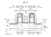
- the memory gate electrode MG is formed on the upper surface TS2 of the region AR2.
- the conductive film 9 is placed on the side surface of the control gate electrode CG on the side opposite to the side where the memory gate electrode MG adjacent to the control gate electrode CG is disposed via the insulating film 8.
- the spacer SP21 made of the remaining conductive film 9 is formed by leaving it in a shape.
- the memory gate electrode MG is formed so as to be adjacent to the control gate electrode CG through the insulating film 8.
- the memory gate electrode MG and the spacer SP21 are formed on the side surfaces opposite to each other of the control gate electrode CG.
- a cap insulating film CP2 is formed on the control gate electrode CG. Therefore, the memory gate electrode MG is formed on the side surface of the cap insulating film CP2 on the side where the memory gate electrode MG adjacent to the control gate electrode CG is disposed via the insulating film 8 so as to form a sidewall spacer shape.
- the conductive film 9 is left.
- the spacer SP21 is a sidewall spacer on the side surface opposite to the side where the memory gate electrode MG adjacent to the control gate electrode CG is disposed, on both sides of the cap insulating film CP2.
- the conductive film 9 is left in the shape.
- An insulating film 8 is interposed between the memory gate electrode MG formed in step S16 and the p-type well PW of the semiconductor substrate 1 and between the memory gate electrode MG and the control gate electrode CG.
- the gate electrode MG is made of a conductive film 9 in contact with the insulating film 8.
- step S16 the portion of the insulating film 8 that is not covered by either the memory gate electrode MG or the spacer SP21 is exposed.
- the insulating film 8 under the memory gate electrode MG becomes a gate insulating film GIm (see FIG. 22 described later) of the memory transistor MT.
- step S17 in FIG. 6 the spacer SP21 is removed.
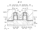
- step S17 first, as shown in FIG. 20, using photolithography, a resist pattern R3 is formed on the semiconductor substrate 1 so that the memory gate electrode MG is covered and the spacer SP21 is exposed.
- a resist film RF3 as a mask film is formed on the insulating film 8 so as to cover the memory gate electrode MG and the spacer SP21.
- the resist film RF3 is patterned to form a resist pattern R3 made of a resist film RF3 that covers the memory gate electrode MG. Then, the spacer SP21 is exposed from the resist film RF3.
- step S17 next, as shown in FIG. 21, the spacer SP21 is removed by dry etching using the formed resist pattern R3 as an etching mask.
- the memory gate electrode MG was covered with the resist pattern R3, it remains without being etched.
- step S18 in FIG. 6 the portion of the insulating film 8 not covered with the memory gate electrode MG is removed by etching.
- portions of the insulating film 8 located between the memory gate electrode MG and the p-type well PW and between the memory gate electrode MG and the control gate electrode CG are left without being removed, and other regions The portion of the insulating film 8 located at is removed.
- a gate insulating film GIm composed of the insulating film 8 between the memory gate electrode MG and the p-type well PW, that is, the semiconductor substrate 1 and between the memory gate electrode MG and the control gate electrode CG is formed.
- step S18 etching can be performed so that the silicon oxide film 8c and the silicon nitride film 8b are removed from the insulating film 8 and the silicon oxide film 8a is left without being removed.
- n ⁇ type semiconductor regions 11a and 11b are formed using an ion implantation method or the like (step S19 in FIG. 6).
- n-type impurities such as arsenic (As) or phosphorus (P) are introduced into the p-type well PW of the semiconductor substrate 1 using the control gate electrode CG and the memory gate electrode MG as a mask.
- n ⁇ type semiconductor regions 11a and 11b are formed in the upper layer portion of p type well PW.
- the n ⁇ type semiconductor region 11a is formed in self alignment with the side surface of the memory gate electrode MG, and the n ⁇ type semiconductor region 11b is formed in self alignment with the side surface of the control gate electrode CG.
- the conductive film is formed in a peripheral circuit region (not shown) different from the memory cell region in which the memory cell MC is formed using, for example, photolithography and etching. 4 (see FIG. 7) may be patterned to form a gate electrode (not shown) made of the conductive film 4.
- the main surface 1a of the semiconductor substrate 1 is made of, for example, a silicon oxide film in the memory cell region.
- An insulating film SIF and a silicon nitride film may be formed.
- the silicon nitride film may be removed.
- the insulating film SIF is formed so as to cover the control gate electrode CG, the cap insulating film CP2, and the memory gate electrode MG in the memory cell region. (See FIG. 24 described later).
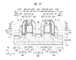
- sidewall spacers SW are formed on the side surface of the control gate electrode CG and the side surface of the memory gate electrode MG (step S20 in FIG. 6).
- an insulating film for the sidewall spacer SW is formed on the entire main surface 1a of the semiconductor substrate 1, and the formed insulating film is etched back by anisotropic etching, for example.
- the sidewall spacer SW is formed by leaving the insulating film in the portion adjacent to the control gate electrode CG on the opposite side of the memory gate electrode MG across the control gate electrode CG. Further, the sidewall spacer SW is formed by leaving the insulating film in a portion adjacent to the memory gate electrode MG on the opposite side of the control gate electrode CG across the memory gate electrode MG.
- These sidewall spacers SW are made of an insulating film such as a silicon oxide film, a silicon nitride film, or a laminated film thereof.
- an insulating film SIF made of, for example, silicon oxide is interposed between the control gate electrode CG and the sidewall spacer SW and between the memory gate electrode MG and the sidewall spacer SW. ing.
- n + -type semiconductor regions 12a and 12b are formed by ion implantation or the like (step S21 in FIG. 6).
- an n-type impurity such as arsenic (As) or phosphorus (P) is used as a semiconductor substrate by using the control gate electrode CG and the memory gate electrode MG and the side wall spacer SW adjacent thereto as a mask. 1 p-type well PW.
- n + type semiconductor regions 12a and 12b are formed in the upper layer portion of p type well PW.
- the n + type semiconductor region 12a is formed in self-alignment with the side wall spacer SW on the side surface of the memory gate electrode MG, and the n + type semiconductor region 12b is formed on the side wall spacer on the side surface of the control gate electrode CG. It is formed in self-alignment with SW.
- the n ⁇ type semiconductor region MS having the LDD structure and functioning as the source region of the memory transistor MT is formed by the n ⁇ type semiconductor region 11a and the n + type semiconductor region 12a having a higher impurity concentration. It is formed.
- the n ⁇ type semiconductor region 11b and the n + type semiconductor region 12b having a higher impurity concentration than the n ⁇ type semiconductor region 11b form an n type semiconductor region MD having an LDD structure and functioning as a drain region of the control transistor CT. .
- activation annealing which is a heat treatment for activating impurities introduced into n ⁇ type semiconductor regions 11a and 11b, n + type semiconductor regions 12a and 12b, and the like is performed.
- the control transistor CT and the memory transistor MT are formed, and the memory cell MC as the nonvolatile memory is formed by the control transistor CT and the memory transistor MT. That is, the control gate electrode CG, the gate insulating film GIc, the memory gate electrode MG, and the gate insulating film GIm form a memory cell MC as a nonvolatile memory. Note that memory cells MC1 and MC2 as two adjacent memory cells MC share the n + -type semiconductor region 12b.
- a metal silicide layer 13, an insulating film 14, an interlayer insulating film 15, and a plug PG are formed (step S22 in FIG. 6).
- a metal film is formed on the entire main surface 1a of the semiconductor substrate 1 so as to cover the cap insulating film CP2, the memory gate electrode MG, and the sidewall spacer SW.
- the metal film is made of, for example, a cobalt (Co) film, a nickel (Ni) film, or a nickel platinum alloy film, and can be formed using a sputtering method or the like.
- heat treatment is performed on the semiconductor substrate 1 to cause the upper layers of the n + type semiconductor regions 12a and 12b and the memory gate electrode MG to react with the metal film.
- metal silicide layers 13 are formed on the n + type semiconductor regions 12a and 12b and the memory gate electrode MG, respectively.
- the metal silicide layer 13 can be, for example, a cobalt silicide layer, a nickel silicide layer, or a platinum-added nickel silicide layer. Thereafter, the unreacted metal film is removed. By performing such a so-called salicide process, the metal silicide layer 13 can be formed on each of the n + type semiconductor regions 12a and 12b and the memory gate electrode MG, as shown in FIG.
- the insulating film 14 is formed so as to cover the cap insulating film CP2, the gate insulating film GIm, the memory gate electrode MG, and the sidewall spacer SW.
- the insulating film 14 is made of, for example, a silicon nitride film.
- the insulating film 14 can be formed by, for example, a CVD method.
- an interlayer insulating film 15 is formed on the insulating film.
- the interlayer insulating film 15 is made of a single film of a silicon oxide film or a laminated film of a silicon nitride film and a silicon oxide film. After the interlayer insulating film 15 is formed by, for example, the CVD method, the upper surface of the interlayer insulating film 15 is planarized.
- step S22 next, as shown in FIG. 27, a plug PG penetrating the interlayer insulating film 15 is formed.
- contact holes CNT are formed in the interlayer insulating film 15 by dry etching the interlayer insulating film 15 using a resist pattern (not shown) formed on the interlayer insulating film 15 by photolithography as an etching mask.
- a conductive plug PG made of tungsten (W) or the like is formed as a conductor portion in the contact hole CNT.
- a barrier conductor film made of, for example, a titanium (Ti) film, a titanium nitride (TiN) film, or a laminated film thereof is formed on the interlayer insulating film 15 including the inside of the contact hole CNT.
- a main conductor film made of tungsten (W) film or the like is formed on the barrier conductor film so as to fill the contact hole CNT, and unnecessary main conductor films and barrier conductor films on the interlayer insulating film 15 are formed by CMP (Chemical Remove by mechanical polishing method or etch back method.
- CMP Chemical Remove by mechanical polishing method or etch back method.
- the contact hole CNT and the plug PG embedded therein are formed on the n + type semiconductor region 12b and the like.
- the metal silicide layer 13 on the n + type semiconductor region 12b is exposed.
- the plug PG embedded in the contact hole CNT is brought into contact with the n + -type semiconductor region 12b on the metal silicide layer 13 formed, n + -type semiconductor region 12b and are electrically connected.
- the plug PG may be electrically connected to the n + type semiconductor region 12a.
- the semiconductor device of the present embodiment is manufactured.
- a wiring having, for example, copper (Cu) as a main conductive film can be formed on the interlayer insulating film 15 in which the plug PG is embedded using, for example, a damascene technique, but the description thereof is omitted here. .
- 28 and 29 are cross-sectional views of a main part of a semiconductor device of a comparative example. 29 is an enlarged view of region RG101 surrounded by a two-dot chain line in the cross-sectional view shown in FIG.
- the semiconductor substrate 1 under the memory gate electrode MG is not dug, and the upper surface TS2 of the region AR2 is the same height as the upper surface TS1 of the region AR1. Placed in position. Further, the area AR3 (see FIG. 1) is not disposed between the area AR1 and the area AR2, and the connection surface TS3 (see FIG. 1) that connects the upper surface TS1 and the upper surface TS2 is not formed.
- the upper surface TS4 of the region AR4 is also arranged at the same height as the upper surface TS1 of the region AR1. Further, the area AR5 (see FIG. 1) is not arranged between the area AR1 and the area AR4, and the connection surface TS5 (see FIG. 1) that connects the upper surface TS1 and the upper surface TS4 is not formed.
- all of the silicon nitride film 8b located between the memory gate electrode MG and the p-type well PW is parallel to the upper surface of the semiconductor substrate 1. Therefore, when data is written by injecting electrons as hot electrons into the silicon nitride film 8b which is a charge storage portion in the insulating film 8 of the memory transistor by using the SSI method, the electrons are stored in the memory gate electrode. It is easy to uniformly inject the silicon nitride film 8b in a portion located between the MG and the p-type well PW. That is, as shown by an arrow ELA in FIG.
- the electron EL is a portion on the semiconductor region MD side as a drain region in a portion of the silicon nitride film 8b located between the memory gate electrode MG and the p-type well PW. In addition to this, it is easy to be injected into a portion on the semiconductor region MS side as a source region.
- the semiconductor device of the comparative example when data is erased by injecting holes into the silicon nitride film 8b by using the above-described FN type tunnel phenomenon, the data between the memory gate electrode MG and the p type well PW is removed. This electric field concentrates on the end portion EP106 on the control gate electrode CG side of the lower surface of the memory gate electrode MG. Therefore, as shown by an arrow HLA in FIG. 29, the holes HL are formed on the p-type well PW side, that is, on the lower side of the silicon nitride film 8b located between the memory gate electrode MG and the control gate electrode CG. Easy to be injected into the part.
- the distribution of electrons injected into the silicon nitride film 8b when writing data is different from the distribution of holes injected into the silicon nitride film 8b when erasing data. Or separated from each other. Therefore, when the writing operation and the erasing operation are repeated many times, the number of holes remaining in the gate insulating film GIm including the silicon nitride film 8b increases, and the retention characteristics (retention characteristics) of the memory cells are reduced. The device characteristics cannot be improved.
- the retention characteristic of a memory cell is a memory when a writing operation and an erasing operation are repeated many times, for example, about 1000 times, and then left at a temperature higher than room temperature, for example, about 150 ° C. for a long time, for example, about 100 hours. It can be evaluated by the change with time of the threshold voltage of the transistor.
- the erase method using the FN type tunnel phenomenon is compared with the erase method using the BTBT phenomenon. As a result, the effect of reducing current consumption becomes significant.
- the erasing method based on the FN type tunnel phenomenon is used, the distribution of holes injected into the silicon nitride film 8b when erasing data is changed into the silicon nitride film 8b when data is written. The problem of being different from the distribution of injected electrons becomes significant. Therefore, the nonvolatile memory cannot be easily miniaturized.
- the upper surface TS2 is lower than the upper surface TS1, and the connection surface TS3 that connects the upper surface TS1 and the upper surface TS2 is formed between the upper surface TS1 and the upper surface TS2.
- the end portion EP1 on the upper surface TS2 side of the connection surface TS3 is disposed on the memory gate electrode MG side in the X-axis direction with respect to the end portion EP2 on the upper surface TS1 side of the connection surface TS3, and the end portion EP2 in the Z-axis direction. It is arranged below.
- a portion of the silicon nitride film 8b located between the memory gate electrode MG and the p-type well PW is connected to a portion P1 (see FIG. 4) formed along the upper surface TS2.
- the electron EL is easily injected into a portion of the silicon nitride film 8b located between the memory gate electrode MG and the p-type well PW on the semiconductor region MD side as a drain region, but as a source region. It is difficult to be injected into the portion on the semiconductor region MS side.
- the memory gate electrode MG includes the electrode part MG1 formed on the upper surface TS2, and the control gate electrode with respect to the electrode part MG1. And an electrode part MG2 formed on the CG side.
- the electrode portion MG2 has a connection surface BS2 as a lower surface that connects the lower surface BS1 of the electrode portion MG1 and the side surface BS3 of the electrode portion MG2 on the control gate electrode CG side.
- the end portion EP5 of the connection surface BS2 of the electrode portion MG2 is connected to the lower surface BS1 of the electrode portion MG1, and the end portion EP6 of the connection surface BS2 of the electrode portion MG2 is connected to the side surface BS3 of the electrode portion MG2.
- the end portion EP5 is disposed on the positive side in the X-axis direction with respect to the end portion EP6, and is disposed below the end portion EP6 in the Z-axis direction.
- corner AP1 is formed by the lower surface BS1 and the connection surface BS2
- corner AP2 is formed by the connection surface BS2 and the side surface BS3.
- the electric field between the memory gate electrode MG and the p type well PW is: Although it concentrates also on edge part EP6, it also concentrates on edge part EP5. Therefore, as indicated by the arrow HLA in FIG. 4, the holes HL are located on the p-type well PW side of the silicon nitride film 8b in the portion located between the memory gate electrode MG and the control gate electrode CG, that is, in the portion P3. That is, in addition to the lower portion, the portion P2 is also injected.
- the semiconductor device of this embodiment even when data is written, electrons are injected into the portion P2 of the silicon nitride film 8b, and even when data is erased, the portion P2 of the silicon nitride film 8b is erased. Holes are injected into the. Therefore, in the semiconductor device of the present embodiment, the distribution of electrons injected into the silicon nitride film 8b when writing data and the distribution of holes injected into the silicon nitride film 8b when erasing data are: Approach each other or be the same.
- the number of holes remaining in the gate insulating film GIm including the silicon nitride film 8b does not increase, so that the retention characteristic (retention characteristic) of the memory cell is deteriorated. This can be prevented or suppressed, and the characteristics of the semiconductor device can be improved.
- the semiconductor substrate has a first surface and a second surface lower than the first surface in the depth direction from the first surface.
- the gate electrode is provided on the first surface
- the memory gate electrode is provided on the second surface.
- the connection surface between the first surface and the second surface is perpendicular to both the first surface and the second surface.
- the technique disclosed in Patent Document 1 described above is a technique for solving the problem that when the width of the memory gate electrode is reduced, the channel length under the memory gate electrode is also shortened and the off-leakage current is increased. It is. Therefore, in the technique disclosed in Patent Document 1, the second surface side end of the connection surface is positioned on the positive side in the X-axis direction with respect to the first surface side end of the connection surface, In addition, it is difficult to incline the connection surface so as to be positioned below the end portion of the connection surface on the first surface side. This is because the channel length under the memory gate electrode is shortened, making it difficult to solve the problem in Patent Document 1.
- FIG. 30 is a main-portion cross-sectional view of the semiconductor device of the first embodiment
- FIG. 31 is a main-portion cross-sectional view of the semiconductor device of the second embodiment
- FIG. 32 is a main-portion cross-section of the semiconductor device of the third embodiment
- FIG. 33 is a fragmentary cross-sectional view of the semiconductor device of Example 4. 30 to 33 show an enlarged view of the periphery of the connection surface TS3 in the cross-sectional view shown in FIG.
- an angle formed by the connection surface TS3 and the upper surface TS2 is defined as an angle ANS1 as an acute angle.
- an obtuse angle between the connection surface TS3 and the upper surface TS2 is represented by an angle ANS1.
- the sum of the angle ANS1 and the angle ANL1 is equal to 180 °.
- connection surface TS3 and the positive side surface SS1 in the X-axis direction of the control gate electrode CG is defined as an acute angle ANS3.
- an obtuse angle between the connection surface TS3 and the side surface SS1 of the control gate electrode CG is represented by an angle ANL3.
- the sum of the angle ANS3 and the angle ANL3 is equal to 180 °.
- the angle ANS1 is equal to the angle formed by the connection surface TS3 and the YZ plane.
- Example 1 shown in FIG. 30 the angle ANS3 is larger than the angle ANS1 (ANS3> ANS1), that is, the angle ANL3 is smaller than the angle ANL1 (ANL3 ⁇ ANL1).
- the angle ANS3 is smaller than the angle ANS1 (ANS3 ⁇ ANS1), that is, the angle ANL3 is larger than the angle ANL1 (ANS3> ANS1).
- Example 1 shown in FIG. 30 when data is written by injecting electrons as hot electrons into the silicon nitride film 8b using the SSI method, the electron EL is as shown by an arrow ELA in FIG. It is easy to be injected into the portion P2 across the connection surface TS3. Further, in the first embodiment shown in FIG. 30, the center in the X-axis direction of the portion P2 is the positive side in the X-axis direction, that is, the memory gate electrode, compared to the second embodiment shown in FIG. 31 and the third embodiment shown in FIG. Located on the MG side. Therefore, although the electron EL is more easily injected into a portion of the silicon nitride film 8b on the semiconductor region MD (see FIG. 4) side as compared with the comparative example, the semiconductor EL is compared with the second and third embodiments. It is difficult to inject into the MD (see FIG. 4) side portion.
- Example 1 shown in FIG. 30 when erasing data by injecting holes into the silicon nitride film 8b using the above-described FN type tunnel phenomenon, the memory gate electrode MG and the p type well PW are erased. Most of the electric field between the two is concentrated on the end EP6, that is, the corner AP2, but a part is also concentrated on the end EP5, that is, the corner AP1. Therefore, as shown by an arrow HLA2 in FIG. 30, most of the holes HL are injected into a portion of the silicon nitride film 8b located around the corner AP2, but some of the holes HL It is also injected into a portion of the silicon nitride film 8b located around the AP1.
- Example 1 shown in FIG. 30 the distribution of electrons injected into the silicon nitride film 8b when writing data and the distribution of holes injected into the silicon nitride film 8b when erasing data are: Although they are closer to each other than the comparative example, they are farther from each other than the second and third embodiments.
- Example 2 shown in FIG. 31 when data is written by injecting electrons as hot electrons into the silicon nitride film 8b using the SSI method, the electron EL is transferred to the arrow ELA in FIG. As shown, it is easy to be injected into the portion P2 across the connection surface TS3. Further, in the second embodiment shown in FIG. 31, compared to the third embodiment shown in FIG. 32, the center in the X-axis direction of the portion P2 is located on the positive side in the X-axis direction, that is, on the memory gate electrode MG side. Compared to Example 1 shown in FIG.
- the center of the portion P3 in the X-axis direction is located on the negative side in the X-axis direction, that is, on the control gate electrode CG side. Therefore, although the electron EL is likely to be injected into the portion of the silicon nitride film 8b on the semiconductor region MD (see FIG. 4) side as compared to the first embodiment, the semiconductor region MD (see FIG. It is difficult to inject into the portion on the side 4).
- Example 2 shown in FIG. 31 when erasing data by injecting holes into the silicon nitride film 8b using the above-described FN type tunnel phenomenon, the memory gate electrode MG and the p type well PW are erased. Are concentrated at the end portion EP5, that is, the corner portion AP1, and the end portion EP6, that is, the corner portion AP2, at substantially the same level. Therefore, of the holes injected into the silicon nitride film 8b, as indicated by the arrow HLA1 in FIG. 31, the ratio of the holes HL injected into the silicon nitride film 8b in the portion located around the corner AP1 is The number is larger than that of the first embodiment, but is smaller than that of the third embodiment.
- the ratio of the holes HL injected into the silicon nitride film 8b in the portion located around the corner AP2 is The number is smaller than that of the first embodiment, but is larger than that of the third embodiment.
- Example 2 shown in FIG. 31 the distribution of electrons injected into the silicon nitride film 8b when writing data and the distribution of holes injected into the silicon nitride film 8b when erasing data are: Although they are closer to each other than the first embodiment, they are far from each other as compared to the third embodiment.
- Example 3 shown in FIG. 32 when data is written by injecting electrons as hot electrons into the silicon nitride film 8b using the SSI method, the electron EL is transferred to the arrow ELA in FIG. As shown, it is easy to be injected into the portion P2 across the connection surface TS3. Also, in the third embodiment shown in FIG. 32, compared to the first embodiment shown in FIG. 30 and the second embodiment shown in FIG. 31, the center in the X-axis direction of the portion P2 is the negative side in the X-axis direction, that is, the control gate. Located on the electrode CG side. Therefore, the electron EL is more likely to be injected into the portion of the silicon nitride film 8b on the semiconductor region MD (see FIG. 4) side as compared with both the first and second embodiments.
- Example 3 shown in FIG. 32 when erasing data by injecting holes into the silicon nitride film 8b using the above-described FN type tunnel phenomenon, the memory gate electrode MG and the p type well PW are erased. The electric field between them is not concentrated on the end EP6, that is, the corner AP2, but concentrated on the end EP5, that is, the corner AP1. Therefore, although some holes HL are injected into a portion of the silicon nitride film 8b located around the corner AP2, most of the holes HL are present at the corner AP1 as indicated by an arrow HLA1 in FIG. Is implanted into a portion of the silicon nitride film 8b located in the periphery of the substrate.
- Example 3 shown in FIG. 32 the distribution of electrons EL injected into the silicon nitride film 8b when data is written and the distribution of holes HL injected into the silicon nitride film 8b when data is erased. are closer to each other or the same as each other as compared to both the first and second embodiments.
- the distribution of electrons injected into the silicon nitride film 8b when writing data and the injection into the silicon nitride film 8b when erasing data are compared.
- the distribution of the generated holes is closer to each other in the order of Example 1, Example 2, and Example 3. Therefore, in the order of the first embodiment, the second embodiment, and the third embodiment, the effect of preventing or suppressing the deterioration of the retention characteristics of the memory cell increases, and the effect of improving the characteristics of the semiconductor device increases.
- the angle ANS3 is 0 °, that is, when the connection surface TS3 is parallel to the YZ plane, the on-current of the control gate transistor decreases. Therefore, it is desirable that the angle ANS3 is greater than zero. That is, it is desirable that the end portion EP1 is disposed on the memory gate electrode MG side in the X-axis direction with respect to the end portion EP2, and is disposed below the end portion EP2 in the Z-axis direction.
- the distribution of electrons injected into the silicon nitride film 8b when writing data and the injection into the silicon nitride film 8b when erasing data are compared.
- the ratio of the part located in the gate electrode CG side increases. Further, when the position of the corner portion AP1 and the position of the corner portion AP2 approach each other, the end portion EP1 is positioned not under the memory gate electrode MG but under the gate insulating film GIm.
- the portion P1 formed along the upper surface TS2 in the silicon nitride film 8b can be increased.
- the thickness of the insulating film 8 on any portion that is, the silicon oxide film 8a, the silicon nitride
- the film thickness of the film 8b and the silicon oxide film 8c can also be made substantially uniform. Therefore, the lower surface BS1 of the electrode portion MG1 is substantially parallel to the upper surface TS2 of the region AR2, and the connection surface BS2 of the electrode portion MG2 is substantially parallel to the connection surface TS3 of the region AR3.
- the shapes of the corner portions AP1 and AP2 of the memory gate electrode MG can be controlled by adjusting the shapes of the step portions formed by the upper surface TS1, the upper surface TS2, and the connection surface TS3. Then, by controlling the shapes of the corners AP1 and AP2 of the memory gate electrode MG, the distribution of electrons injected into the silicon nitride film 8b when writing data and the injection into the silicon nitride film 8b when erasing data are performed. The distribution of generated holes can be made closer to each other.
- the angle ANS1 as an acute angle is defined as the angle formed by the connection surface BS2 with the lower surface BS1
- the angle ANS3 as the acute angle is defined as an angle formed between the connection surface BS2 and the side surface BS3. Even in this case, the same tendency can be obtained between Example 1 and Example 3. That is, the distribution of electrons injected into the silicon nitride film 8b when writing data and the distribution of holes injected into the silicon nitride film 8b when erasing data are shown in the first, second, and second embodiments. In the order of Example 3, they are closer together.
- Example 4 shown in FIG. 33 the upper end portion of the side surface SS1 of the control gate electrode CG is positioned opposite to the memory gate electrode MG with respect to the lower end portion of the side surface SS1 in the X-axis direction.
- an angle formed by the connection surface TS3 and the upper surface TS2 is defined as an acute angle ANL1
- an angle formed by the connection surface TS3 and the side surface SS1 of the control gate electrode CG is defined as an acute angle ANS3.
- the angle ANS3 is smaller than the angle ANS1 (ANS3 ⁇ ANS1), that is, the angle ANL3 is larger than the angle ANL1 (ANL3> ANL1). Show the case.
- Example 4 shown in FIG. 33 the angle ANS3 is further reduced by the angle AS compared to the case where the side surface SS1 of the control gate electrode CG is parallel to the YZ plane. Therefore, the condition of the third embodiment which is the most preferable condition described with reference to FIG. 32, that is, the angle ANS3 ⁇ angle ANS1 is easily satisfied, and the distribution of electrons injected into the silicon nitride film 8b when data is written The distribution of holes injected into the silicon nitride film 8b when erasing data is closer to each other. Therefore, it is possible to further prevent or suppress the remaining of holes in the charge storage portion, and to further improve the retention characteristics of the memory cell.
- FIG. 34 is a cross-sectional view of a principal part of the semiconductor device of Example 5. 34 shows an enlarged view of the periphery of the connection surface TS3 in the cross-sectional view shown in FIG.
- the length L1 is longer than the length L2 in the X-axis direction of the upper surface TS2 of the portion located under the gate insulating film GIm.
- the ratio of the portion P2 in the silicon nitride film 8b that intersects the direction in which electrons injected as hot electrons move using the SSI method moves.
- the ratio can be increased as compared with the ratio of the portion P1, which is a portion parallel to the direction of coming. Therefore, by injecting electrons into the silicon nitride film 8b by using the SSI method, electrons are easily injected into the portion P2 across the connection surface TS3 when writing data. That is, from the viewpoint of adjusting the distribution of electrons injected in the data write operation, the length L1 of the connection surface TS3 is made longer than the length L2 of the upper surface TS2 of the portion located under the gate insulating film GIm. Is preferred.
- the gate length of the memory gate electrode MG can be easily shortened. This is advantageous for memory miniaturization.
- a length L3 as a distance between the end portion EP6 and the end portion EP6 is shorter than a length L4 of the lower surface BS1 of the electrode portion MG1 in the X-axis direction.
- the corner portion AP1 and the corner portion AP2 which are portions where the electric field between the memory gate electrode MG and the p-type well PW is concentrated, can be brought close to each other. Therefore, by injecting holes into the silicon nitride film 8b using the FN type tunnel phenomenon, holes can be reliably injected into the portion P2 of the silicon nitride film 8b when erasing data. That is, from the viewpoint of adjusting the distribution of holes injected in the data erasing operation, it is preferable that the length L3 of the connection surface BS2 is shorter than the length L4 of the lower surface BS1.
- the length L1 is set to the end EP2 and the end EP11 (see FIG. 3).
- the length L2 can be defined as the distance in the X-axis direction between the end of the gate insulating film GIm opposite to the control gate electrode CG side and the end EP11.
- the length L3 is set to the end EP6 and the end EP51 (see FIG. 3).
- the length L4 can be defined as the distance in the X-axis direction between the end portion of the memory gate electrode MG opposite to the control gate electrode CG side and the end portion EP51.
- the semiconductor substrate includes a region AR3 arranged between the region AR1 and the region AR2, the control gate electrode CG is formed on the upper surface TS1 of the region AR1, and the memory gate electrode MG Is formed on the upper surface TS2 of the region AR2.
- the upper surface TS2 is lower than the upper surface TS1, and the region AR3 has a connection surface TS3 that connects the upper surface TS1 and the upper surface TS2.
- Gate insulating films GIm are formed between the memory gate electrode MG and the control gate electrode CG, between the memory gate electrode MG and the upper surface TS2, and between the memory gate electrode MG and the connection surface TS3.
- the end portion EP1 on the upper surface TS2 side of the connection surface TS3 is disposed on the memory gate electrode MG side with respect to the end portion EP2 on the upper surface TS1 side of the connection surface TS3, and is disposed below the end portion EP2.
- the distribution of electrons injected into the silicon nitride film 8b when writing data and the distribution of holes injected into the silicon nitride film 8b when erasing data are close to each other or the same. become. Therefore, even when the write operation and the erase operation are repeated many times, the number of holes remaining in the gate insulating film GIm including the silicon nitride film 8b does not increase, so that the retention characteristics of the memory cell can be improved. The characteristics of the semiconductor device can be improved.
Landscapes
- Non-Volatile Memory (AREA)
- Semiconductor Memories (AREA)
- Chemical & Material Sciences (AREA)
- Chemical Kinetics & Catalysis (AREA)
- General Chemical & Material Sciences (AREA)
Abstract
Description
<半導体装置の構造>
初めに、本実施の形態の半導体装置の構造について説明する。図1~図4は、実施の形態の半導体装置の要部断面図である。図2~図4に示す断面図は、図1に示す断面図のうち二点鎖線で囲まれた領域RG1を拡大して示す。なお、図2~図4では、n-型半導体領域VMG、金属シリサイド層13、絶縁膜14および層間絶縁膜15の図示を省略する。
次に、本実施の形態の半導体装置の製造方法について説明する。図5および図6は、実施の形態の半導体装置の製造工程の一部を示すプロセスフロー図である。図7~図27は、実施の形態の半導体装置の製造工程中の要部断面図である。
次に、電荷蓄積部としての窒化シリコン膜8bに注入された電子および正孔の分布について、比較例と対比しながら説明する。
次に、接続面TS3の傾斜角の好適な範囲について、実施例1~実施例4を比較しながら説明する。図30は、実施例1の半導体装置の要部断面図であり、図31は、実施例2の半導体装置の要部断面図であり、図32は、実施例3の半導体装置の要部断面図であり、図33は、実施例4の半導体装置の要部断面図である。図30~図33に示す断面図は、図4に示す断面図のうち、接続面TS3の周辺を拡大して示す。
次に、接続面TS3の長さおよびメモリゲート電極MGの下面の長さの好適な範囲について、実施例5を参照しながら説明する。図34は、実施例5の半導体装置の要部断面図である。図34に示す断面図は、図4に示す断面図のうち、接続面TS3の周辺を拡大して示す。
本実施の形態の半導体装置では、半導体基板は、領域AR1と領域AR2との間に配置された領域AR3を含み、制御ゲート電極CGは、領域AR1の上面TS1上に形成され、メモリゲート電極MGは、領域AR2の上面TS2上に形成されている。上面TS2は、上面TS1よりも低く、領域AR3は、上面TS1と上面TS2とを接続する接続面TS3を有する。メモリゲート電極MGと制御ゲート電極CGとの間、メモリゲート電極MGと上面TS2との間、および、メモリゲート電極MGと接続面TS3との間には、ゲート絶縁膜GImが形成されている。接続面TS3の上面TS2側の端部EP1が、接続面TS3の上面TS1側の端部EP2に対してメモリゲート電極MG側に配置され、端部EP2よりも下方に配置されている。
1a 主面
3、5、6、8、14 絶縁膜
4、9 導電膜
7 膜
8a、8c 酸化シリコン膜
8b 窒化シリコン膜
11a、11b n-型半導体領域
12a、12b n+型半導体領域
13 金属シリサイド層
15 層間絶縁膜
ANL1~ANL3、ANS1~ANS3、AS 角度
AP1、AP2 角部
AR 活性領域
AR1~AR5 領域
BS1 下面
BS11、BS21 平面
BS2 接続面
BS3 側面
CG 制御ゲート電極
CNT コンタクトホール
CP1、CP2 キャップ絶縁膜
CT 制御トランジスタ
EL 電子
ELA、HLA、HLA1、HLA2 矢印
EP1、EP11、EP2~EP5、EP51、EP6 端部
FT1 膜厚
GIc、GIm ゲート絶縁膜
HL 正孔
IT1 間隔
L1~L4 長さ
MC、MC1、MC2 メモリセル
MD、MS 半導体領域
MG メモリゲート電極
MG1、MG2 電極部
MT メモリトランジスタ
P1~P3 部分
PG プラグ
PW p型ウェル
R1~R3 レジストパターン
RF1~RF3 レジスト膜
RG1、RG2 領域
SIF 絶縁膜
SOF1、SOF2 犠牲酸化膜
SP11、SP12、SP21 スペーサ
SS1 側面
SW サイドウォールスペーサ
TS1、TS2、TS4 上面
TS21、TS31 平面
TS3、TS5 接続面
VMG n-型半導体領域
Claims (15)
- 半導体基板と、
前記半導体基板の主面上に形成された第1ゲート電極と、
前記第1ゲート電極と前記半導体基板との間に形成された第1ゲート絶縁膜と、
前記半導体基板上に形成され、前記第1ゲート電極と隣り合う第2ゲート電極と、
前記第2ゲート電極と前記半導体基板との間、および、前記第2ゲート電極と前記第1ゲート電極との間に形成され、内部に電荷蓄積部を有する第2ゲート絶縁膜と、
を有し、
前記半導体基板は、前記主面側の第1領域、第2領域および第3領域を含み、
前記第2領域は、平面視において、前記第1領域に対して第1方向における第1の側に配置され、
前記第3領域は、前記第1領域と前記第2領域との間に配置され、
前記第1ゲート電極は、前記第1領域の第1上面上に形成され、
前記第2ゲート電極は、前記第2領域の第2上面上に形成され、
前記第2上面は、前記第1上面よりも低く、
前記第3領域は、前記第1上面と前記第2上面とを接続する第1接続面を有し、
前記第2ゲート絶縁膜は、前記第1接続面上、および、前記第2上面上に形成され、
前記第1接続面の第1端部は、前記第2上面と接続され、
前記第1接続面の前記第1端部と反対側の第2端部は、前記第1上面と接続され、
前記第1端部は、前記第2端部に対して前記第1方向における前記第1の側に配置され、かつ、前記第2端部よりも下方に配置されている、半導体装置。 - 請求項1記載の半導体装置において、
前記半導体基板は、前記主面側の第4領域を含み、
前記第4領域は、平面視において、前記第1領域に対して前記第1方向における前記第1の側と反対側に配置され、
前記第4領域の第3上面は、前記第1上面よりも低く、
前記第2上面は、前記第3上面よりも低い、半導体装置。 - 請求項2記載の半導体装置において、
前記半導体基板は、前記主面側の第5領域を含み、
前記第5領域は、前記第1領域と前記第4領域との間に配置され、
前記第5領域は、前記第1上面と前記第3上面とを接続する第2接続面を有し、
前記第2接続面の第3端部は、前記第3上面と接続され、
前記第2接続面の前記第3端部と反対側の第4端部は、前記第1上面と接続され、
前記第3端部は、前記第4端部に対して前記第1方向における前記第1の側と反対側に配置され、かつ、前記第4端部よりも下方に配置されている、半導体装置。 - 請求項3記載の半導体装置において、
前記第1接続面が前記第2上面となす鋭角の角度は、前記第2接続面が前記第3上面となす鋭角の角度よりも大きい、半導体装置。 - 請求項1記載の半導体装置において、
前記第1接続面が、前記第1ゲート電極の前記第1方向における前記第1の側の第1側面となす鋭角の角度は、前記第1接続面が前記第2上面となす鋭角の角度よりも小さい、半導体装置。 - 請求項1記載の半導体装置において、
前記第1ゲート電極は、平面視において、前記第1方向と直交する第2方向に延在し、
前記第2方向に垂直な断面において、前記第1端部と前記第2端部との距離は、前記第2ゲート絶縁膜下に位置する部分の前記第2上面の、前記第1方向における長さよりも長い、半導体装置。 - 請求項1記載の半導体装置において、
前記第2ゲート電極は、
前記第2上面上に形成された第1電極部と、
前記第1電極部に対して前記第1ゲート電極側に形成された第2電極部と、
を含み、
前記第2電極部は、前記第1電極部の第1下面と、前記第2電極部の前記第1ゲート電極側の第2側面とを接続する第2下面を有し、
前記第2下面の第5端部は、前記第1電極部の前記第1下面と接続され、
前記第2下面の前記第5端部と反対側の第6端部は、前記第2側面と接続され、
前記第5端部は、前記第6端部に対して前記第1方向における前記第1の側に配置され、かつ、前記第6端部よりも下方に配置されており、
前記第1ゲート電極は、平面視において、前記第1方向と直交する第3方向に延在し、
前記第3方向に垂直な断面において、前記第2下面に平行な方向における前記第2下面の長さは、前記第1方向における前記第1下面の長さよりも短い、半導体装置。 - 請求項1記載の半導体装置において、
前記第1ゲート電極と前記第1ゲート絶縁膜と前記第2ゲート電極と前記第2ゲート絶縁膜とによりメモリが形成されている、半導体装置。 - (a)半導体基板を用意する工程、
(b)前記半導体基板の主面上に第1ゲート電極を形成し、前記第1ゲート電極と前記半導体基板との間に第1ゲート絶縁膜を形成する工程、
(c)前記半導体基板上、および、前記第1ゲート電極の表面に、内部に電荷蓄積部を有する絶縁膜を形成する工程、
(d)前記絶縁膜上に、導電膜を形成する工程、
(e)前記導電膜をエッチバックすることにより、平面視において、前記第1ゲート電極の第1方向における第1の側の第1側面に前記絶縁膜を介して前記導電膜を残して第2ゲート電極を形成し、前記第2ゲート電極と前記半導体基板との間、および、前記第2ゲート電極と前記第1ゲート電極との間の前記絶縁膜からなる第2ゲート絶縁膜を形成する工程、
を有し、
前記(a)工程では、前記主面側の第1領域、第2領域および第3領域を含む前記半導体基板を用意し、
前記第2領域は、平面視において、前記第1領域に対して前記第1方向における前記第1の側に配置され、
前記第3領域は、前記第1領域と前記第2領域との間に配置され、
前記(b)工程では、前記第1領域の第1上面上に前記第1ゲート電極を形成し、
前記(c)工程は、
(c1)前記第2領域および前記第3領域をエッチングすることにより、前記第2領域の第2上面を、前記第1上面よりも低くし、前記第3領域に、前記第1上面と前記第2上面とを接続する第1接続面を形成する工程、
(c2)前記(c1)工程の後、前記第2上面上、前記第1接続面上、および、前記第1ゲート電極の表面に、前記絶縁膜を形成する工程、
を含み、
前記(e)工程では、前記第2上面上に前記第2ゲート電極を形成し、
前記第1接続面の第1端部は、前記第2上面と接続され、
前記第1接続面の前記第1端部と反対側の第2端部は、前記第1上面と接続され、
前記第1端部は、前記第2端部に対して前記第1方向における前記第1の側に配置され、かつ、前記第2端部よりも下方に配置される、半導体装置の製造方法。 - 請求項9記載の半導体装置の製造方法において、
(f)前記(b)工程の後、前記(c)工程の前に、前記第1ゲート電極の前記第1側面と反対側の第2側面に第1側壁部を形成する工程、
を有し、
前記(f)工程は、
(f1)前記半導体基板上に、前記第1ゲート電極を覆うように、第1膜を形成する工程、
(f2)前記第1膜をエッチバックすることにより、前記第1ゲート電極の前記第2側面に前記第1膜を残して前記第1側壁部を形成する工程、
を含み、
前記(c1)工程では、前記第1ゲート電極および前記第1側壁部をマスクとして前記第2領域および前記第3領域をエッチングすることにより、前記第2上面を、前記第1上面よりも低くし、
前記(c)工程は、さらに、
(c3)前記(c2)工程の後、前記第1側壁部を除去する工程、
を含む、半導体装置の製造方法。 - 請求項10記載の半導体装置の製造方法において、
前記(f2)工程では、前記第1膜をエッチバックすることにより、前記第1ゲート電極の前記第2側面に前記第1側壁部を形成し、前記第1ゲート電極の前記第1側面に前記第1膜を残して第2側壁部を形成し、
前記(f)工程は、さらに、
(f3)前記半導体基板上に、前記第1側壁部および前記第2側壁部を覆うように、マスク膜を形成する工程、
(f4)前記マスク膜をパターニングし、前記第1側壁部を覆う前記マスク膜からなるマスクパターンを形成し、前記第2側壁部を前記マスク膜から露出させる工程、
(f5)前記(f4)工程の後、前記第2側壁部を除去する工程、
(f6)前記(f5)工程の後、前記マスクパターンを除去する工程、
を含む、半導体装置の製造方法。 - 請求項9記載の半導体装置の製造方法において、
前記(a)工程では、前記主面側の第4領域を含む前記半導体基板を用意し、
前記第4領域は、平面視において、前記第1領域に対して前記第1方向における前記第1の側と反対側に配置され、
前記半導体装置の製造方法は、さらに、
(g)前記(b)工程の後、前記(c)工程の前に、前記第4領域の表面を酸化することにより、前記第4領域の第3上面を、前記第1領域の前記第1上面よりも低くする工程、
を有し、
前記(c1)工程では、前記第2領域および前記第3領域をエッチングすることにより、前記第2上面を、前記第3上面よりも低くする、半導体装置の製造方法。 - 請求項12記載の半導体装置の製造方法において、
前記(a)工程では、前記主面側の第5領域を含む前記半導体基板を用意し、
前記第5領域は、前記第1領域と前記第4領域との間に配置され、
前記(g)工程では、前記第5領域に、前記第1上面と前記第3上面とを接続する第2接続面を形成し、
前記第2接続面の第3端部は、前記第3上面と接続され、
前記第2接続面の前記第3端部と反対側の第4端部は、前記第1上面と接続され、
前記第3端部は、前記第4端部に対して前記第1方向における前記第1の側と反対側に配置され、かつ、前記第4端部よりも下方に配置される、半導体装置の製造方法。 - 請求項13記載の半導体装置の製造方法において、
前記第1接続面が前記第2上面となす鋭角の角度は、前記第2接続面が前記第3上面となす鋭角の角度よりも大きい、半導体装置の製造方法。 - 請求項9記載の半導体装置の製造方法において、
前記(b)工程では、前記第1ゲート電極上にキャップ絶縁膜を形成し、
前記(c1)工程では、前記キャップ絶縁膜をマスクとして前記第2領域および前記第3領域をエッチングすることにより、前記第2上面を、前記第1上面よりも低くする、半導体装置の製造方法。
Priority Applications (6)
| Application Number | Priority Date | Filing Date | Title |
|---|---|---|---|
| KR1020177001980A KR20170130344A (ko) | 2015-03-30 | 2015-03-30 | 반도체 장치 및 그 제조 방법 |
| CN201580051068.5A CN106716637A (zh) | 2015-03-30 | 2015-03-30 | 半导体器件及其制造方法 |
| US15/512,475 US10192965B2 (en) | 2015-03-30 | 2015-03-30 | Semiconductor device including first and second gate electrodes and method for manufacturing the same |
| PCT/JP2015/060023 WO2016157393A1 (ja) | 2015-03-30 | 2015-03-30 | 半導体装置およびその製造方法 |
| JP2017508910A JP6275920B2 (ja) | 2015-03-30 | 2015-03-30 | 半導体装置およびその製造方法 |
| TW104143240A TW201707149A (zh) | 2015-03-30 | 2015-12-22 | 半導體裝置及其製造方法 |
Applications Claiming Priority (1)
| Application Number | Priority Date | Filing Date | Title |
|---|---|---|---|
| PCT/JP2015/060023 WO2016157393A1 (ja) | 2015-03-30 | 2015-03-30 | 半導体装置およびその製造方法 |
Publications (1)
| Publication Number | Publication Date |
|---|---|
| WO2016157393A1 true WO2016157393A1 (ja) | 2016-10-06 |
Family
ID=57004826
Family Applications (1)
| Application Number | Title | Priority Date | Filing Date |
|---|---|---|---|
| PCT/JP2015/060023 Ceased WO2016157393A1 (ja) | 2015-03-30 | 2015-03-30 | 半導体装置およびその製造方法 |
Country Status (6)
| Country | Link |
|---|---|
| US (1) | US10192965B2 (ja) |
| JP (1) | JP6275920B2 (ja) |
| KR (1) | KR20170130344A (ja) |
| CN (1) | CN106716637A (ja) |
| TW (1) | TW201707149A (ja) |
| WO (1) | WO2016157393A1 (ja) |
Families Citing this family (2)
| Publication number | Priority date | Publication date | Assignee | Title |
|---|---|---|---|---|
| US10991704B2 (en) * | 2018-12-27 | 2021-04-27 | Globalfoundries Singapore Pte. Ltd. | Memory device and a method for forming the memory device |
| CN110783461B (zh) * | 2019-09-18 | 2023-08-25 | 北京元芯碳基集成电路研究院 | 晶体管及其制造方法 |
Citations (5)
| Publication number | Priority date | Publication date | Assignee | Title |
|---|---|---|---|---|
| JP2001148434A (ja) * | 1999-10-12 | 2001-05-29 | New Heiro:Kk | 不揮発性メモリセルおよびその使用方法、製造方法ならびに不揮発性メモリアレイ |
| JP2001168219A (ja) * | 1999-09-29 | 2001-06-22 | Sony Corp | 不揮発性半導体記憶装置およびその駆動方法 |
| JP2004303918A (ja) * | 2003-03-31 | 2004-10-28 | Renesas Technology Corp | 半導体装置の製造方法および半導体装置 |
| JP2008053498A (ja) * | 2006-08-25 | 2008-03-06 | Renesas Technology Corp | 半導体装置およびその製造方法 |
| WO2008059768A1 (en) * | 2006-11-14 | 2008-05-22 | Nec Corporation | Semiconductor device |
Family Cites Families (8)
| Publication number | Priority date | Publication date | Assignee | Title |
|---|---|---|---|---|
| US6388293B1 (en) * | 1999-10-12 | 2002-05-14 | Halo Lsi Design & Device Technology, Inc. | Nonvolatile memory cell, operating method of the same and nonvolatile memory array |
| US6469935B2 (en) * | 1999-08-05 | 2002-10-22 | Halo Lsi Design & Device Technology, Inc. | Array architecture nonvolatile memory and its operation methods |
| JP2003078041A (ja) * | 2001-08-31 | 2003-03-14 | Matsushita Electric Ind Co Ltd | 半導体記憶装置及びその製造方法 |
| TW527652B (en) * | 2002-02-06 | 2003-04-11 | Taiwan Semiconductor Mfg | Manufacturing method of selection gate for the split gate flash memory cell and its structure |
| JP5014591B2 (ja) | 2005-05-24 | 2012-08-29 | ルネサスエレクトロニクス株式会社 | 半導体装置及びその製造方法 |
| JP5402633B2 (ja) * | 2007-08-09 | 2014-01-29 | 日本電気株式会社 | 不揮発性半導体記憶装置 |
| JP5164520B2 (ja) * | 2007-10-19 | 2013-03-21 | ルネサスエレクトロニクス株式会社 | 不揮発性半導体メモリ及びデータプログラム/消去方法 |
| US9331160B2 (en) * | 2013-08-20 | 2016-05-03 | Freescale Semiconductor, Inc. | Split-gate non-volatile memory cells having gap protection zones |
-
2015
- 2015-03-30 WO PCT/JP2015/060023 patent/WO2016157393A1/ja not_active Ceased
- 2015-03-30 KR KR1020177001980A patent/KR20170130344A/ko not_active Abandoned
- 2015-03-30 CN CN201580051068.5A patent/CN106716637A/zh active Pending
- 2015-03-30 US US15/512,475 patent/US10192965B2/en active Active
- 2015-03-30 JP JP2017508910A patent/JP6275920B2/ja active Active
- 2015-12-22 TW TW104143240A patent/TW201707149A/zh unknown
Patent Citations (5)
| Publication number | Priority date | Publication date | Assignee | Title |
|---|---|---|---|---|
| JP2001168219A (ja) * | 1999-09-29 | 2001-06-22 | Sony Corp | 不揮発性半導体記憶装置およびその駆動方法 |
| JP2001148434A (ja) * | 1999-10-12 | 2001-05-29 | New Heiro:Kk | 不揮発性メモリセルおよびその使用方法、製造方法ならびに不揮発性メモリアレイ |
| JP2004303918A (ja) * | 2003-03-31 | 2004-10-28 | Renesas Technology Corp | 半導体装置の製造方法および半導体装置 |
| JP2008053498A (ja) * | 2006-08-25 | 2008-03-06 | Renesas Technology Corp | 半導体装置およびその製造方法 |
| WO2008059768A1 (en) * | 2006-11-14 | 2008-05-22 | Nec Corporation | Semiconductor device |
Also Published As
| Publication number | Publication date |
|---|---|
| US20170278938A1 (en) | 2017-09-28 |
| TW201707149A (zh) | 2017-02-16 |
| CN106716637A (zh) | 2017-05-24 |
| KR20170130344A (ko) | 2017-11-28 |
| JPWO2016157393A1 (ja) | 2017-06-01 |
| US10192965B2 (en) | 2019-01-29 |
| JP6275920B2 (ja) | 2018-02-07 |
Similar Documents
| Publication | Publication Date | Title |
|---|---|---|
| JP5592214B2 (ja) | 半導体装置の製造方法 | |
| US10600799B2 (en) | Memory device and low breakdown voltage transistor | |
| US10043814B2 (en) | Semiconductor substrate with a single protruding portion with multiple different widths and insulation thickness | |
| US9349743B2 (en) | Method of manufacturing semiconductor device | |
| US9905429B2 (en) | Semiconductor device and a manufacturing method thereof | |
| CN103035650A (zh) | 半导体装置以及半导体装置的制造方法 | |
| JP6998267B2 (ja) | 半導体装置およびその製造方法 | |
| US10192879B2 (en) | Semiconductor device and manufacturing method thereof | |
| JP2018195718A (ja) | 半導体装置およびその製造方法 | |
| CN109994542A (zh) | 半导体器件及其制造方法 | |
| JP6275920B2 (ja) | 半導体装置およびその製造方法 | |
| JP6594198B2 (ja) | 半導体装置およびその製造方法 | |
| TW201841348A (zh) | 半導體裝置及其製造方法 | |
| US10312254B2 (en) | Semiconductor device and a manufacturing method thereof | |
| JP2012069652A (ja) | 半導体装置およびその製造方法 | |
| JP2012094790A (ja) | 半導体装置およびその製造方法 | |
| JP2016157728A (ja) | 半導体装置の製造方法 | |
| JP2022082914A (ja) | 半導体装置およびその製造方法 |
Legal Events
| Date | Code | Title | Description |
|---|---|---|---|
| 121 | Ep: the epo has been informed by wipo that ep was designated in this application |
Ref document number: 15887546 Country of ref document: EP Kind code of ref document: A1 |
|
| ENP | Entry into the national phase |
Ref document number: 20177001980 Country of ref document: KR Kind code of ref document: A |
|
| ENP | Entry into the national phase |
Ref document number: 2017508910 Country of ref document: JP Kind code of ref document: A |
|
| WWE | Wipo information: entry into national phase |
Ref document number: 15512475 Country of ref document: US |
|
| NENP | Non-entry into the national phase |
Ref country code: DE |
|
| 122 | Ep: pct application non-entry in european phase |
Ref document number: 15887546 Country of ref document: EP Kind code of ref document: A1 |