WO2016149961A1 - 不等行驱动宽度的液晶面板的源极驱动器及源极驱动方法 - Google Patents
不等行驱动宽度的液晶面板的源极驱动器及源极驱动方法 Download PDFInfo
- Publication number
- WO2016149961A1 WO2016149961A1 PCT/CN2015/075850 CN2015075850W WO2016149961A1 WO 2016149961 A1 WO2016149961 A1 WO 2016149961A1 CN 2015075850 W CN2015075850 W CN 2015075850W WO 2016149961 A1 WO2016149961 A1 WO 2016149961A1
- Authority
- WO
- WIPO (PCT)
- Prior art keywords
- data signal
- output channel
- signal output
- electrically connected
- thin film
- Prior art date
- Legal status (The legal status is an assumption and is not a legal conclusion. Google has not performed a legal analysis and makes no representation as to the accuracy of the status listed.)
- Ceased
Links
Images

Classifications
-
- G—PHYSICS
- G09—EDUCATION; CRYPTOGRAPHY; DISPLAY; ADVERTISING; SEALS
- G09G—ARRANGEMENTS OR CIRCUITS FOR CONTROL OF INDICATING DEVICES USING STATIC MEANS TO PRESENT VARIABLE INFORMATION
- G09G3/00—Control arrangements or circuits, of interest only in connection with visual indicators other than cathode-ray tubes
- G09G3/20—Control arrangements or circuits, of interest only in connection with visual indicators other than cathode-ray tubes for presentation of an assembly of a number of characters, e.g. a page, by composing the assembly by combination of individual elements arranged in a matrix no fixed position being assigned to or needed to be assigned to the individual characters or partial characters
- G09G3/34—Control arrangements or circuits, of interest only in connection with visual indicators other than cathode-ray tubes for presentation of an assembly of a number of characters, e.g. a page, by composing the assembly by combination of individual elements arranged in a matrix no fixed position being assigned to or needed to be assigned to the individual characters or partial characters by control of light from an independent source
- G09G3/36—Control arrangements or circuits, of interest only in connection with visual indicators other than cathode-ray tubes for presentation of an assembly of a number of characters, e.g. a page, by composing the assembly by combination of individual elements arranged in a matrix no fixed position being assigned to or needed to be assigned to the individual characters or partial characters by control of light from an independent source using liquid crystals
- G09G3/3611—Control of matrices with row and column drivers
- G09G3/3685—Details of drivers for data electrodes
- G09G3/3688—Details of drivers for data electrodes suitable for active matrices only
-
- G—PHYSICS
- G09—EDUCATION; CRYPTOGRAPHY; DISPLAY; ADVERTISING; SEALS
- G09G—ARRANGEMENTS OR CIRCUITS FOR CONTROL OF INDICATING DEVICES USING STATIC MEANS TO PRESENT VARIABLE INFORMATION
- G09G2310/00—Command of the display device
- G09G2310/02—Addressing, scanning or driving the display screen or processing steps related thereto
- G09G2310/0232—Special driving of display border areas
-
- G—PHYSICS
- G09—EDUCATION; CRYPTOGRAPHY; DISPLAY; ADVERTISING; SEALS
- G09G—ARRANGEMENTS OR CIRCUITS FOR CONTROL OF INDICATING DEVICES USING STATIC MEANS TO PRESENT VARIABLE INFORMATION
- G09G2310/00—Command of the display device
- G09G2310/02—Addressing, scanning or driving the display screen or processing steps related thereto
- G09G2310/0264—Details of driving circuits
- G09G2310/0297—Special arrangements with multiplexing or demultiplexing of display data in the drivers for data electrodes, in a pre-processing circuitry delivering display data to said drivers or in the matrix panel, e.g. multiplexing plural data signals to one D/A converter or demultiplexing the D/A converter output to multiple columns
-
- G—PHYSICS
- G09—EDUCATION; CRYPTOGRAPHY; DISPLAY; ADVERTISING; SEALS
- G09G—ARRANGEMENTS OR CIRCUITS FOR CONTROL OF INDICATING DEVICES USING STATIC MEANS TO PRESENT VARIABLE INFORMATION
- G09G2310/00—Command of the display device
- G09G2310/06—Details of flat display driving waveforms
-
- G—PHYSICS
- G09—EDUCATION; CRYPTOGRAPHY; DISPLAY; ADVERTISING; SEALS
- G09G—ARRANGEMENTS OR CIRCUITS FOR CONTROL OF INDICATING DEVICES USING STATIC MEANS TO PRESENT VARIABLE INFORMATION
- G09G2310/00—Command of the display device
- G09G2310/08—Details of timing specific for flat panels, other than clock recovery
-
- G—PHYSICS
- G09—EDUCATION; CRYPTOGRAPHY; DISPLAY; ADVERTISING; SEALS
- G09G—ARRANGEMENTS OR CIRCUITS FOR CONTROL OF INDICATING DEVICES USING STATIC MEANS TO PRESENT VARIABLE INFORMATION
- G09G2330/00—Aspects of power supply; Aspects of display protection and defect management
- G09G2330/02—Details of power systems and of start or stop of display operation
- G09G2330/021—Power management, e.g. power saving
Definitions
- the present invention relates to the field of display technologies, and in particular, to a source driver and a source driving method for a liquid crystal panel having unequal row driving widths.
- LCDs liquid crystal displays
- Various consumer electronic products such as digital assistants, digital cameras, notebook computers, and desktop computers have become mainstream in display devices.
- the active matrix liquid crystal display includes a plurality of horizontally extending scan lines and data lines extending in a vertical direction, and multiple scans. A plurality of pixel regions are intersected by the line and the plurality of data lines, and each pixel region is provided with one pixel, and each pixel has a Thin Film Transistor (TFT).
- TFT Thin Film Transistor
- the source driver 2 includes first and second shift registers 211 and 212, first and second main latch circuits 221 and 222, First and second latch circuits 231, 232, first and second potential converting circuits 241, 242, first and second digital to analog converting circuits 251, 252, first and second output buffer circuits 261, 262 And first and second output circuits 271, 272.
- the first shift register 211, the first main latch circuit 221, the first latch circuit 231, the first potential conversion circuit 241, the first digital to analog conversion circuit 251, the first output buffer circuit 261, and the first An output circuit 271 constitutes a signal path 281, and the source drive signal generated by the signal path 281 is transmitted to the corresponding pixel through the data line, so that the pixel emits light.
- the above-mentioned existing source drivers have the same row driving width for each scan, and cannot be dynamically adjusted, and are only applicable to a conventional rectangular display.
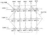
- FIG. 2 is a schematic diagram of a pixel arrangement of an irregular display panel, the irregular display panel comprising a total of 15 pixels from a pixel pixel (1, 1) to a pixel (3, 5), wherein the display pixel is located in the display area.
- the remaining pixels are not display pixels, input data signals to the non-display pixels will cause waste of energy, so the source driver needs to be able to adjust the number of display pixels required for each row Line drive width to save energy.
- Another object of the present invention is to provide a source driving method for a liquid crystal panel having unequal row driving widths, which can dynamically adjust a row driving width in each line scanning so that data signals are transmitted only in pixels that need to be displayed in each row, and It is not transmitted to pixels that do not need to be displayed in each line. It is suitable for non-rectangular display and can reduce the output power consumption of the LCD panel.
- the present invention first provides a source driver for a liquid crystal panel having unequal row driving widths, comprising: an input signal decoding control unit, and a plurality of data signals electrically connected to the input signal decoding control unit Output channel
- the input signal decoding control unit receives a data signal output channel start address signal, a data signal output channel abort address signal, and a data signal input timing control signal;
- the input signal decoding control unit outputs a data signal output timing control signal
- the input signal decoding control unit adjusts the row driving width for each scan according to the received data signal output channel start address signal and the data signal output channel stop address signal control start data signal output channel.
- the input signal decoding control unit includes a composite switch module, and the composite switch module includes a first thin film transistor, a second thin film transistor, and a third reverse thin film transistor;
- the gate of the first thin film transistor is electrically connected to the data signal output channel start address signal, the source is electrically connected to the data signal input timing control signal, and the drain is electrically connected to the data signal output channel corresponding to the start address.
- the gate of the second thin film transistor is electrically connected to the data signal output channel stop address signal, the source is electrically connected to the data signal output timing control signal, and the drain is electrically connected to the data signal output channel corresponding to the stop address.
- the gate of the third reverse thin film transistor is electrically connected to the data signal output channel start address signal, the source is electrically connected to the drain of the first thin film transistor, and the drain is electrically connected to the drain of the second thin film transistor. pole.
- the data signal output channel start address signal and the data signal output channel stop address signal are encoded in a packet of the data signal transmission, and are transmitted together with the data signal.
- a length setting mode is added by modifying a decoding extension of the mini-LVDS transmission protocol for transmitting a data signal output channel start address signal and a data signal output channel abort address signal.
- the channel start address signal and the data signal output channel abort address signal are decoded by a 3-wire to 8-line decoding circuit for the data signal encoded in the packet of the data signal transmission.
- the data signal output channel includes: a shift register electrically connected to the input signal decoding control unit, a main latch circuit, a secondary latch circuit electrically connected to the main latch circuit, and a secondary latch circuit electrically connected a potential conversion circuit, a digital to analog conversion circuit electrically connected to the potential conversion circuit, an output buffer circuit electrically connected to the digital to analog conversion circuit, and an output circuit electrically connected to the output buffer circuit.
- the present invention also provides a source driver for a liquid crystal panel having an unequal row drive width, comprising: an input signal decoding control unit; and a plurality of data signal output channels electrically connected to the input signal decoding control unit;
- the input signal decoding control unit receives a data signal output channel start address signal, a data signal output channel abort address signal, and a data signal input timing control signal;
- the input signal decoding control unit outputs a data signal output timing control signal
- the input signal decoding control unit adjusts the row driving width at each scan according to the received data signal output channel start address signal and the data signal output channel stop address signal control start data signal output channel;
- the input signal decoding control unit includes a composite switch module, and the composite switch module includes a first thin film transistor, a second thin film transistor, and a third reverse thin film transistor;
- the gate of the first thin film transistor is electrically connected to the data signal output channel start address signal, the source is electrically connected to the data signal input timing control signal, and the drain is electrically connected to the data signal output channel corresponding to the start address.
- the gate of the second thin film transistor is electrically connected to the data signal output channel stop address signal, the source is electrically connected to the data signal output timing control signal, and the drain is electrically connected to the data signal output channel corresponding to the stop address.
- the gate of the third reverse thin film transistor is electrically connected to the data signal output channel start address signal, the source is electrically connected to the drain of the first thin film transistor, and the drain is electrically connected to the second thin The drain of the film transistor;
- the data signal output channel includes: a shift register electrically connected to the input signal decoding control unit, a main latch circuit, a secondary latch circuit electrically connected to the main latch circuit, and a secondary latch circuit electrical a connected potential conversion circuit, a digital to analog conversion circuit electrically connected to the potential conversion circuit, an output buffer circuit electrically connected to the digital to analog conversion circuit, and an output circuit electrically connected to the output buffer circuit.
- the invention also provides a source driving method for a liquid crystal panel with unequal row driving width, comprising the following steps:
- Step 1 Providing a source driver of a liquid crystal panel having an unequal row driving width
- the source driver of the liquid crystal panel of the unequal row driving width comprises: an input signal decoding control unit; and a plurality of data signal output channels electrically connected to the input signal decoding control unit;
- Step 2 inputting a data signal output channel start address signal, a data signal output channel abort address signal, and a data signal input timing control signal to the input signal decoding control unit;
- Step 3 The input signal decoding control unit decodes the received data signal output channel start address signal, and the data signal output channel abort address signal, and sets a data signal output channel start address and a data signal output channel abort address;
- Step 4 Input a data signal to a data signal channel corresponding to the data signal output channel start address and the data signal output channel abort address, and transmit the data signal to a corresponding pixel.
- the input signal decoding control unit includes a composite switch module, and the composite switch module includes a first thin film transistor, a second thin film transistor, and a third reverse thin film transistor;
- the gate of the first thin film transistor is electrically connected to the data signal output channel start address signal, the source is electrically connected to the data signal input timing control signal, and the drain is electrically connected to the data signal output channel corresponding to the start address.
- the gate of the second thin film transistor is electrically connected to the data signal output channel stop address signal, the source is electrically connected to the data signal output timing control signal, and the drain is electrically connected to the data signal output channel corresponding to the stop address.
- the gate of the third reverse thin film transistor is electrically connected to the data signal output channel start address signal, the source is electrically connected to the drain of the first thin film transistor, and the drain is electrically connected to the drain of the second thin film transistor. pole.
- the data signal output channel start address signal and the data signal output channel stop address signal in the step 2 are encoded in a packet of the data signal transmission, and are transmitted together with the data signal.
- the step 2 increases a length by modifying the decoding extension of the mini-LVDS transmission protocol.
- the mode is set for transmitting a data signal output channel start address signal and a data signal output channel abort address signal.
- the present invention provides a source driver and a source driving method for a liquid crystal panel having unequal row driving widths, by providing an input signal decoding control unit electrically connected to a plurality of data signal output channels, and The data signal output channel start address signal and the data signal output channel suspension address signal are encoded in a packet of the data signal transmission, and sent to the input signal decoding control unit, and the input signal decoding control unit outputs the channel according to the received data signal.
- the start address signal and the data signal output channel stop address signal control start the number of data signal output channels to adjust the row drive width per scan, and can dynamically adjust the row drive width of each line scan, so that the data signal is only Each row needs to be transmitted in the displayed pixels, and is not transmitted to the pixels in each row that need not be displayed. It is suitable for non-rectangular display, reducing the output power consumption of the liquid crystal panel, and the liquid crystal panel of the unequal row driving width
- the source driver is designed based on the existing drive architecture and has a simple structure.
- Figure 1 is a schematic structural view of a conventional source driver
- FIG. 2 is a schematic view showing a pixel arrangement of an irregular liquid crystal panel
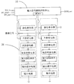
- FIG. 3 is a schematic structural view of a source driver of a liquid crystal panel of unequal row driving width according to the present invention
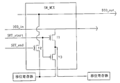
- FIG. 4 is a circuit diagram of a composite switch module in a source driver of a liquid crystal panel of unequal row driving width according to the present invention
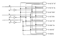
- FIG. 5 is a circuit diagram of a decoding circuit in a source driver of a liquid crystal panel of unequal row driving width according to the present invention
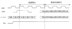
- FIG. 6 is a waveform diagram of a conventional mini-LVDS transmission protocol
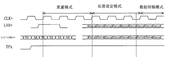
- FIG. 7 is a waveform diagram of an improved mini-LVDS transmission protocol according to the present invention.
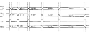
- Figure 8 is a diagram showing output waveforms when transmitted according to the mini-LVDS transmission protocol shown in Figure 7;
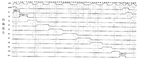
- Figure 9 is a waveform diagram showing the row drive width of the source driver of the liquid crystal panel of the unequal row drive width of the present invention.
- the present invention first provides a source driver for a liquid crystal panel having unequal row driving widths, including: an input signal decoding control unit 10, and a plurality of electrical connection with the input signal decoding control unit 10; Data signal output channel 20.
- the input signal decoding control unit 10 receives a data signal output channel start address signal SET_start, a data signal output channel abort address signal SET_end, and a data signal input timing control signal DIO_in; the input signal decoding control unit 10 outputs a data signal output timing Control signal DIO_out; the input signal decoding control unit 10 adjusts each scan according to the received data signal output channel start address signal SET_start and the data signal output channel stop address signal SET_end control start data signal output channel 20 The row drive width.
- the data signal output channel 20 includes: a shift register electrically connected to the input signal decoding control unit 10, a main latch circuit, a secondary latch circuit electrically connected to the main latch circuit, and a secondary latch a potential conversion circuit electrically connected to the circuit, a digital to analog conversion circuit electrically connected to the potential conversion circuit, an output buffer circuit electrically connected to the digital to analog conversion circuit, and an output circuit electrically connected to the output buffer circuit.
- the input signal decoding control unit 10 includes a composite switch module SW_MUX, and the composite switch module SW_MUX includes a first thin film transistor T1, a second thin film transistor T2, and a third reverse thin film transistor T3.
- the gate of the first thin film transistor T1 is electrically connected to the data signal output channel start address signal SET_start, the source is electrically connected to the data signal input timing control signal DIO_in, and the drain is electrically connected to the data corresponding to the start address.
- a shift register of the signal output channel and a source of the third reverse thin film transistor T3 a gate of the second thin film transistor T2 is electrically connected to the data signal output channel stop address signal SET_end, and the source is electrically connected to the data signal Output timing control signal DIO_out, the drain is electrically connected to the shift register of the data signal output channel corresponding to the stop address and the drain of the third reverse thin film transistor T3; the gate electrical property of the third reverse thin film transistor T3
- the signal is connected to the data signal output channel start address signal SET_start, the source is electrically connected to the drain of the first thin film transistor T1, and the drain is electrically connected to the drain of the second thin film transistor T2.
- the data signal output channel start address signal SET_start and the data signal output channel stop address signal SET_end are encoded in a packet of the data signal Data transmission, and are transmitted together with the data signal Data.
- the number is transmitted by improving the mini-LVDS transmission protocol According to the signal output channel start address signal SET_start, the data signal output channel stop address signal SET_end, and the data signal.
- the mini-LVDS transmission mode is generally divided into two types: reset RESET and data transmission DataSampling.
- the present invention improves the mini-LVDS transmission mode in the usual sense by modifying the mini-LVDS transmission protocol.
- the decoding topology is added to a length setting mode LENGTH DEFINE for transmitting the data signal output channel start address signal SET_start and the data signal output channel abort address signal SET_end.
- the data signal output channel start address signal SET_start encoded in the packet transmitted by the data signal Data is decoded by a decoding circuit, and the data signal output channel abort address signal SET_end is decoded to obtain a data signal output channel start address and a data signal output channel. Abort the address.
- FIG. 5 is a circuit diagram of a 3-wire to 8-wire decoding circuit according to the present invention.
- the input end of the decoding circuit includes first, second, and third input channels, and each channel is divided into positive The channel and the reverse channel, that is, the first, second, and third forward input channels D0, D1, D2, the first, second, and third inverting input channels D0', D1', D2'.
- the output end of the decoding circuit includes first to eighth output channels Y0 to Y7, and each output channel is from the first, second, and third forward input channels D0, D1, D2 and the first and second, Three of the six reverse input channels D0', D1', D2' receive input signals, and the combinations of the three channels of the input signals received by each output channel are different.
- the signals transmitted from the first, second, and third inverting input channels D0', D1', and D2' are all "1"
- the signals input to the first, second, and third input channels are all "0.”
- the input signals of the decoding circuit are the data signal output channel start address signal SET_start, and the data signal output channel abort address.
- Signal SET_end is the data signal output channel start address signal SET_start.
- the present invention further provides a source driving method of the liquid crystal panel with unequal row driving width, comprising the following steps:
- Step 1 Please refer to FIG. 3 and FIG. 4 simultaneously to provide a source driver of a liquid crystal panel having an unequal row driving width.
- the source driver of the liquid crystal panel of the unequal row driving width includes an input signal decoding control unit 10 and a plurality of data signal output channels 20 electrically connected to the input signal decoding control unit 10.
- the data signal output channel 20 includes: a shift register electrically connected to the input signal decoding control unit 10, a main latch circuit, a secondary latch circuit electrically connected to the main latch circuit, and a secondary latch circuit electrical a connected potential conversion circuit, a digital to analog conversion circuit electrically connected to the potential conversion circuit, an output buffer circuit electrically connected to the digital to analog conversion circuit, and an output circuit electrically connected to the output buffer circuit.
- the input signal decoding control unit 10 includes a composite switch module SW_MUX, and the composite switch module SW_MUX includes a first thin film transistor T1, a second thin film transistor T2, and a third reverse thin film transistor T3.
- the gate of the first thin film transistor T1 is electrically connected to the data signal output channel start address signal SET_start, the source is electrically connected to the data signal input timing control signal DIO_in, and the drain is electrically connected to the data corresponding to the start address.
- a shift register of the signal output channel and a source of the third reverse thin film transistor T3 a gate of the second thin film transistor T2 is electrically connected to the data signal output channel stop address signal SET_end, and the source is electrically connected to the data signal Output timing control signal DIO_out, the drain is electrically connected to the shift register of the data signal output channel corresponding to the stop address and the drain of the third reverse thin film transistor T3; the gate electrical property of the third reverse thin film transistor T3
- the signal is connected to the data signal output channel start address signal SET_start, the source is electrically connected to the drain of the first thin film transistor T1, and the drain is electrically connected to the drain of the second thin film transistor T2.
- Step 2 The input signal decoding control unit 10 inputs a data signal output channel start address signal SET_start, a data signal output channel abort address signal SET_end, and a data signal input timing control signal DIO_in.
- the data signal output channel start address signal SET_start and the data signal output channel stop address signal SET_end are encoded in the packet of the data signal Data transmission, and the number According to the signal Data transmission.
- a length setting mode LENGTH DEFINE is added by modifying a decoding extension of the mini-LVDS transmission protocol, and the length setting mode LENGTH DEFINE is used to transmit a data signal output channel start address signal SET_start, and a data signal output channel.
- the address signal SET_end is aborted.
- Step 3 The input signal decoding control unit 10 decodes the received data signal output channel start address signal SET_start, and the data signal output channel suspension address signal SET_end, sets the data signal output channel start address and the data signal output channel. Abort the address.
- the data signal output channel start address signal SET_start encoded in the packet encoded by the data signal Data is decoded by a 3-wire to 8-line decoding circuit as shown in FIG. 5, and the data signal output channel abort address signal SET_end is decoded. , get the data signal output channel start address and data signal output channel stop address.
- Step 4 Input a data signal Data to the data signal channel 20 corresponding to the data signal output channel start address and the data signal output channel abort address, and transmit the data signal Data to the corresponding pixel.
- FIG. 8 is an output waveform diagram when transmitting by the mini-LVDS transmission protocol improved by the present invention
- FIG. 9 is a waveform diagram of the row driving width of the source driver of the present invention.
- the row drive width of the output of the present invention changes with the change of the start address of the data signal output channel and the stop address of the data signal output channel, thereby realizing dynamic adjustment of the row drive width in each line scan.
- the source driver and the source driving method of the liquid crystal panel of the unequal row driving width of the present invention decode the control unit by setting an input signal electrically connected to the plurality of data signal output channels, and output the data signal.
- the channel start address signal and the data signal output channel stop address signal are encoded in the packet of the data signal transmission, and sent to the input signal decoding control unit, and the input signal decoding control unit outputs the channel start address signal according to the received data signal.
- the number of data signal output channels controlled by the data signal output channel abort address signal control to adjust the row drive width for each scan, and can dynamically adjust the row drive width of each line scan so that the data signal needs to be displayed only in each line.
- the pixels are transmitted without being transmitted to each row of pixels that need not be displayed, suitable for non-rectangular display, reducing the output power consumption of the liquid crystal panel, and the source driver of the liquid crystal panel of the unequal row drive width is based on
- the existing drive architecture design has a simple structure.
Landscapes
- Engineering & Computer Science (AREA)
- Chemical & Material Sciences (AREA)
- Crystallography & Structural Chemistry (AREA)
- Physics & Mathematics (AREA)
- Computer Hardware Design (AREA)
- General Physics & Mathematics (AREA)
- Theoretical Computer Science (AREA)
- Control Of Indicators Other Than Cathode Ray Tubes (AREA)
- Liquid Crystal Display Device Control (AREA)
- Liquid Crystal (AREA)
Abstract
一种不等行驱动宽度的液晶面板的源极驱动器(2)及源极驱动方法,通过设置与多个数据信号输出通道(20)电性连接的输入信号解码控制单元(10),并将数据信号输出通道起始地址信号(SET_start)、与数据信号输出通道中止地址信号(SET_end)编码于数据信号(Data)传输的封包中,发送给输入信号解码控制单元(10),输入信号解码控制单元(10)根据接收到的数据信号输出通道起始地址信号(SET_start)、与数据信号输出通道中止地址信号(SET_end)控制启动的数据信号输出通道(20)的数量来调整每次扫描时的行驱动宽度,能够动态调整每一行扫描时的行驱动宽度,使得数据信号(Data)仅在每一行需要显示的像素中传输,适用于非矩形显示,减少了液晶面板的输出功耗;且该不等行驱动宽度的液晶面板的源极驱动器(2)基于现有驱动架构设计,结构简单。
Description
本发明涉及显示技术领域,尤其涉及一种不等行驱动宽度的液晶面板的源极驱动器及源极驱动方法。
随着显示技术的发展,液晶显示器(Liquid Crystal Display,LCD)等平面显示装置因具有高画质、省电、机身薄及应用范围广等优点,而被广泛的应用于手机、电视、个人数字助理、数字相机、笔记本电脑、台式计算机等各种消费性电子产品,成为显示装置中的主流。
主动矩阵式液晶显示器(Active Matrix Liquid Crystal Display,AMLCD)是目前最常用的显示装置,所述主动矩阵式液晶显示器包含多条水平方向延伸的扫描线和沿垂直方向延伸的数据线,多条扫描线与多条数据线的交叉出多个像素区域,每一像素区域内设有一个像素,每个像素具有一个薄膜晶体管(Thin Film Transistor,TFT)。所述扫描线电性连接于栅极驱动器,用于传输扫描信号,所述数据线电性连接于源极驱动器,用于传输数据信号。如果在水平方向的某一扫描线上施加足够的正电压,则会使得该条扫描线上的所有TFT打开,此时该条扫描线上的像素电极会与垂直方向的数据线连接,将数据线上的所加载的数据信号电压写入像素中,从而显示画面。
图1为现有的源极驱动器的结构示意图,如图1所示,源极驱动器2包含有第一、第二移位寄存器211、212、第一、第二主栓锁电路221、222、第一、第二次栓锁电路231、232、第一、第二电位转换电路241、242、第一、第二数字至模拟转换电路251、252、第一、第二输出缓冲电路261、262、及第一、第二输出电路271、272。其中,第一移位寄存器211、第一主栓锁电路221、第一次栓锁电路231、第一电位转换电路241、第一数字至模拟转换电路251、第一输出缓冲电路261、及第一输出电路271构成信号通道281,信号通道281所生成的源极驱动信号通过数据线传输到对应像素,使得像素发光。上述现有的源极驱动器每次扫描时行驱动宽度均相同,无法动态调整,仅适用于传统的矩形显示器。
然而,随着显示技术的不断发展,用户对非矩形显示器的需求也越来越多,在非矩形显示器中,由于其显示形状不规则,所以其一行进行显示
的像素数量也不相同。以图2所示为一种不规则显示面板的像素排列示意图,该不规则显示面板包括像素pixel(1,1)至pixel(3,5)共15颗像素,其中位于显示区域内的显示像素为第一行的pixel(1,2)至pixel(1,4)三颗,第二行的pixel(2,1)至pixel(2,5)五颗,第三行的pixel(3,2)至pixel(3,4)三颗,其余像素均为不显示像素,向不显示像素输入数据信号将造成能耗的浪费,因此需要源极驱动器能够根据每一行所需的显示像素数量调整其行驱动宽度,以节省能耗。
发明内容
本发明的目的在于提供一种不等行驱动宽度的液晶面板的源极驱动器,能够动态调整每一行扫描时的行驱动宽度,使得数据信号仅在每一行需要显示的像素中传输,而不会传输到每一行不需要显示的像素中,适用于非矩形显示,并能够减少液晶面板的输出功耗。
本发明的目的还在于提供一种不等行驱动宽度的液晶面板的源极驱动方法,能够动态调整每一行扫描时的行驱动宽度,使得数据信号仅在每一行需要显示的像素中传输,而不会传输到每一行不需要显示的像素中,适用于非矩形显示,并能够减少液晶面板的输出功耗。
为实现上述目的,本发明首先提供一种不等行驱动宽度的液晶面板的源极驱动器,包括:一输入信号解码控制单元、及与所述输入信号解码控制单元电性连接的多个数据信号输出通道;
所述输入信号解码控制单元接收数据信号输出通道起始地址信号、数据信号输出通道中止地址信号、及数据信号输入时序控制信号;
所述输入信号解码控制单元输出数据信号输出时序控制信号;
所述输入信号解码控制单元根据接收到的数据信号输出通道起始地址信号、及数据信号输出通道中止地址信号控制启动的数据信号输出通道的数量来调整每次扫描时的行驱动宽度。
所述输入信号解码控制单元包括一复合开关模块,所述复合开关模块包括第一薄膜晶体管、第二薄膜晶体管、及第三反向薄膜晶体管;
所述第一薄膜晶体管的栅极电性连接于数据信号输出通道起始地址信号,源极电性连接于数据信号输入时序控制信号,漏极电性连接于对应起始地址的数据信号输出通道的移位寄存器及第三反向薄膜晶体管的源极;
所述第二薄膜晶体管的栅极电性连接于数据信号输出通道中止地址信号,源极电性连接于数据信号输出时序控制信号,漏极电性连接于对应中止地址的数据信号输出通道的移位寄存器及第三反向薄膜晶体管的漏极;
所述第三反向薄膜晶体管的栅极电性连接于数据信号输出通道起始地址信号,源极电性连接于第一薄膜晶体管的漏极,漏极电性连接于第二薄膜晶体管的漏极。
所述数据信号输出通道起始地址信号、及数据信号输出通道中止地址信号编码于数据信号传输的封包中,与数据信号共同传输。
通过修改mini-LVDS传输协议的解码拓谱来增加一长度设定模式,所述长度设定模式用于传输数据信号输出通道起始地址信号、与数据信号输出通道中止地址信号。
通过一3线至8线解码电路对编码于数据信号传输的封包中的数据信号输出通道起始地址信号、与数据信号输出通道中止地址信号进行解码。
所述数据信号输出通道包括:与输入信号解码控制单元电性连接的移位寄存器及主栓锁电路、与主栓锁电路电性连接的次栓锁电路、与次栓锁电路电性连接的电位转换电路、与电位转换电路电性连接的数字至模拟转换电路、与数字至模拟转换电路电性连接的输出缓冲电路、及与输出缓冲电路电性连接的输出电路。
本发明还提供一种不等行驱动宽度的液晶面板的源极驱动器,包括:一输入信号解码控制单元、及与所述输入信号解码控制单元电性连接的多个数据信号输出通道;
所述输入信号解码控制单元接收数据信号输出通道起始地址信号、数据信号输出通道中止地址信号、及数据信号输入时序控制信号;
所述输入信号解码控制单元输出数据信号输出时序控制信号;
所述输入信号解码控制单元根据接收到的数据信号输出通道起始地址信号、及数据信号输出通道中止地址信号控制启动的数据信号输出通道的数量来调整每次扫描时的行驱动宽度;
其中,所述输入信号解码控制单元包括一复合开关模块,所述复合开关模块包括第一薄膜晶体管、第二薄膜晶体管、及第三反向薄膜晶体管;
所述第一薄膜晶体管的栅极电性连接于数据信号输出通道起始地址信号,源极电性连接于数据信号输入时序控制信号,漏极电性连接于对应起始地址的数据信号输出通道的移位寄存器及第三反向薄膜晶体管的源极;
所述第二薄膜晶体管的栅极电性连接于数据信号输出通道中止地址信号,源极电性连接于数据信号输出时序控制信号,漏极电性连接于对应中止地址的数据信号输出通道的移位寄存器及第三反向薄膜晶体管的漏极;
所述第三反向薄膜晶体管的栅极电性连接于数据信号输出通道起始地址信号,源极电性连接于第一薄膜晶体管的漏极,漏极电性连接于第二薄
膜晶体管的漏极;
其中,所述数据信号输出通道包括:与输入信号解码控制单元电性连接的移位寄存器及主栓锁电路、与主栓锁电路电性连接的次栓锁电路、与次栓锁电路电性连接的电位转换电路、与电位转换电路电性连接的数字至模拟转换电路、与数字至模拟转换电路电性连接的输出缓冲电路、及与输出缓冲电路电性连接的输出电路。
本发明还提供一种不等行驱动宽度的液晶面板的源极驱动方法,包括如下步骤:
步骤1、提供一不等行驱动宽度的液晶面板的源极驱动器;
该不等行驱动宽度的液晶面板的源极驱动器包括:一输入信号解码控制单元、及与所述输入信号解码控制单元电性连接的多个数据信号输出通道;
步骤2、向所述输入信号解码控制单元输入数据信号输出通道起始地址信号、数据信号输出通道中止地址信号、及数据信号输入时序控制信号;
步骤3、所述输入信号解码控制单元解码所接收到的数据信号输出通道起始地址信号、与数据信号输出通道中止地址信号,设定数据信号输出通道起始地址和数据信号输出通道中止地址;
步骤4、向对应所述数据信号输出通道起始地址和数据信号输出通道中止地址之间的数据信号通道输入数据信号,并将所述数据信号传输到对应的像素。
所述输入信号解码控制单元包括一复合开关模块,所述复合开关模块包括第一薄膜晶体管、第二薄膜晶体管、及第三反向薄膜晶体管;
所述第一薄膜晶体管的栅极电性连接于数据信号输出通道起始地址信号,源极电性连接于数据信号输入时序控制信号,漏极电性连接于对应起始地址的数据信号输出通道的移位寄存器及第三反向薄膜晶体管的源极;
所述第二薄膜晶体管的栅极电性连接于数据信号输出通道中止地址信号,源极电性连接于数据信号输出时序控制信号,漏极电性连接于对应中止地址的数据信号输出通道的移位寄存器及第三反向薄膜晶体管的漏极;
所述第三反向薄膜晶体管的栅极电性连接于数据信号输出通道起始地址信号,源极电性连接于第一薄膜晶体管的漏极,漏极电性连接于第二薄膜晶体管的漏极。
所述步骤2中数据信号输出通道起始地址信号、及数据信号输出通道中止地址信号编码于数据信号传输的封包中,与数据信号共同传输。
所述步骤2通过修改mini-LVDS传输协议的解码拓谱来增加一长度设
定模式,所述长度设定模式用于传输数据信号输出通道起始地址信号、与数据信号输出通道中止地址信号。
本发明的有益效果:本发明提供的一种不等行驱动宽度的液晶面板的源极驱动器及源极驱动方法,通过设置与多个数据信号输出通道电性连接的输入信号解码控制单元,并将数据信号输出通道起始地址信号、与数据信号输出通道中止地址信号编码于数据信号传输的封包中,发送给输入信号解码控制单元,所述输入信号解码控制单元根据接收到的数据信号输出通道起始地址信号、与数据信号输出通道中止地址信号控制启动的数据信号输出通道的数量来调整每次扫描时的行驱动宽度,能够动态调整每一行扫描时的行驱动宽度,使得数据信号仅在每一行需要显示的像素中传输,而不会传输到每一行不需显示的像素中,适用于非矩形显示,减少了液晶面板的输出功耗,且所述不等行驱动宽度的液晶面板的源极驱动器基于现有驱动架构设计,结构简单。
为了能更进一步了解本发明的特征以及技术内容,请参阅以下有关本发明的详细说明与附图,然而附图仅提供参考与说明用,并非用来对本发明加以限制。
下面结合附图,通过对本发明的具体实施方式详细描述,将使本发明的技术方案及其它有益效果显而易见。
附图中,
图1现有的源极驱动器的结构示意图;
图2为一种不规则液晶面板的像素排列示意图;
图3为本发明的不等行驱动宽度的液晶面板的源极驱动器的结构示意图;
图4为本发明的不等行驱动宽度的液晶面板的源极驱动器中复合开关模块的电路图;
图5为本发明的不等行驱动宽度的液晶面板的源极驱动器中一种解码电路的电路图;
图6为现有的mini-LVDS传输协议的波形图;
图7为本发明对mini-LVDS传输协议进行改进后的波形图;
图8为根据图7所示mini-LVDS传输协议传输时的输出波形图;
图9为本发明的不等行驱动宽度的液晶面板的源极驱动器的行驱动宽度波形图。
为更进一步阐述本发明所采取的技术手段及其效果,以下结合本发明的优选实施例及其附图进行详细描述。
请参阅图3,本发明首先提供一种不等行驱动宽度的液晶面板的源极驱动器,包括:一输入信号解码控制单元10、及与所述输入信号解码控制单元10电性连接的多个数据信号输出通道20。
所述输入信号解码控制单元10接收数据信号输出通道起始地址信号SET_start、数据信号输出通道中止地址信号SET_end、及数据信号输入时序控制信号DIO_in;所述输入信号解码控制单元10输出数据信号输出时序控制信号DIO_out;所述输入信号解码控制单元10根据接收到的数据信号输出通道起始地址信号SET_start、及数据信号输出通道中止地址信号SET_end控制启动的数据信号输出通道20的数量来调整每次扫描时的行驱动宽度。
具体地,所述数据信号输出通道20包括:与输入信号解码控制单元10电性连接的移位寄存器及主栓锁电路、与主栓锁电路电性连接的次栓锁电路、与次栓锁电路电性连接的电位转换电路、与电位转换电路电性连接的数字至模拟转换电路、与数字至模拟转换电路电性连接的输出缓冲电路、及与输出缓冲电路电性连接的输出电路。
请参阅图4,所述输入信号解码控制单元10包括一复合开关模块SW_MUX,所述复合开关模块SW_MUX包括第一薄膜晶体管T1、第二薄膜晶体管T2、及第三反向薄膜晶体管T3。所述第一薄膜晶体管T1的栅极电性连接于数据信号输出通道起始地址信号SET_start,源极电性连接于数据信号输入时序控制信号DIO_in,漏极电性连接于对应起始地址的数据信号输出通道的移位寄存器及第三反向薄膜晶体管T3的源极;所述第二薄膜晶体管T2的栅极电性连接于数据信号输出通道中止地址信号SET_end,源极电性连接于数据信号输出时序控制信号DIO_out,漏极电性连接于对应中止地址的数据信号输出通道的移位寄存器及第三反向薄膜晶体管T3的漏极;所述第三反向薄膜晶体管T3的栅极电性连接于数据信号输出通道起始地址信号SET_start,源极电性连接于第一薄膜晶体管T1的漏极,漏极电性连接于第二薄膜晶体管T2的漏极。
进一步地,所述数据信号输出通道起始地址信号SET_start、及数据信号输出通道中止地址信号SET_end编码于数据信号Data传输的封包中,与数据信号Data共同传输。优选的,通过改进mini-LVDS传输协议来传输数
据信号输出通道起始地址信号SET_start、数据信号输出通道中止地址信号SET_end、及数据信号。请参阅图6,通常mini-LVDS传输模式分为重置RESET与数据传输DataSampling两种,请参阅图7,本发明对通常意义上的mini-LVDS传输模式进行改进,通过修改mini-LVDS传输协议的解码拓谱(protocol)来增加一长度设定模式LENGTH DEFINE,所述长度设定模式LENGTH DEFINE用于传输数据信号输出通道起始地址信号SET_start、与数据信号输出通道中止地址信号SET_end。
通过一解码电路对编码于数据信号Data传输的封包中的数据信号输出通道起始地址信号SET_start、与数据信号输出通道中止地址信号SET_end进行解码,得到数据信号输出通道起始地址和数据信号输出通道中止地址。
具体的,请参阅图5,图5为本发明的一种3线至8线解码电路的电路图,该解码电路的输入端包括第一、第二、第三输入通道,每条通道分为正向通道与反向通道,即第一、第二、第三正向输入通道D0、D1、D2,第一、第二、第三反向输入通道D0’、D1’、D2’。数字信号“0”与“1”经过正向通道传输时,信号不变;经过反向通道传输时,“0”将会被反向为“1”,“1”将会被反向为“0”。所述解码电路的输出端包括第一至第八个输出通道Y0至Y7,每一输出通道均从第一、第二、第三正向输入通道D0、D1、D2与第一、第二、第三反向输入通道D0’、D1’、D2’这六条通道中的三条接收输入信号,且每一输出通道接收的输入信号的三条通道的组合不同。以第一输出通道Y0为例,第一输出通道Y0接收第一、第二、第三反向输入通道D0’、D1’、D2’传来的信号,即Y0=D0’D1’D2’;当第一、第二、第三反向输入通道D0’、D1’、D2’传来的信号均为“1”,即向第一、第二、第三输入通道输入的信号均为“0”时,即向所述解码电路输入“3’b000”信号时,有Y0=1,第一输出通道Y0启用,以控制相对应地址的数据信号输出通道打开。类似的,所有解码电路的输入信号与启用的输出通道之间的关系如下表1所示,所述解码电路的输入信号即为数据信号输出通道起始地址信号SET_start、与数据信号输出通道中止地址信号SET_end。
| D2D1D0 | Y0 | Y1 | Y2 | Y3 | Y4 | Y5 | Y6 | Y7 |
| 3’b000 | 1 | |||||||
| 3’b001 | 1 | |||||||
| 3’b010 | 1 | |||||||
| 3’b011 | 1 |
| 3’b100 | 1 | |||||||
| 3’b101 | 1 | |||||||
| 3’b110 | 1 | |||||||
| 3’b111 | 1 |
表1
在上述不等行驱动宽度的液晶面板的源极驱动器的基础上,本发明还提供一种不等行驱动宽度的液晶面板的源极驱动方法,包括如下步骤:
步骤1、请同时参阅图3、图4,提供一不等行驱动宽度的液晶面板的源极驱动器。
该不等行驱动宽度的液晶面板的源极驱动器包括:一输入信号解码控制单元10、及与所述输入信号解码控制单元10电性连接的多个数据信号输出通道20。
所述数据信号输出通道20包括:与输入信号解码控制单元10电性连接的移位寄存器及主栓锁电路、与主栓锁电路电性连接的次栓锁电路、与次栓锁电路电性连接的电位转换电路、与电位转换电路电性连接的数字至模拟转换电路、与数字至模拟转换电路电性连接的输出缓冲电路、及与输出缓冲电路电性连接的输出电路。
所述输入信号解码控制单元10包括一复合开关模块SW_MUX,所述复合开关模块SW_MUX包括第一薄膜晶体管T1、第二薄膜晶体管T2、及第三反向薄膜晶体管T3。所述第一薄膜晶体管T1的栅极电性连接于数据信号输出通道起始地址信号SET_start,源极电性连接于数据信号输入时序控制信号DIO_in,漏极电性连接于对应起始地址的数据信号输出通道的移位寄存器及第三反向薄膜晶体管T3的源极;所述第二薄膜晶体管T2的栅极电性连接于数据信号输出通道中止地址信号SET_end,源极电性连接于数据信号输出时序控制信号DIO_out,漏极电性连接于对应中止地址的数据信号输出通道的移位寄存器及第三反向薄膜晶体管T3的漏极;所述第三反向薄膜晶体管T3的栅极电性连接于数据信号输出通道起始地址信号SET_start,源极电性连接于第一薄膜晶体管T1的漏极,漏极电性连接于第二薄膜晶体管T2的漏极。
步骤2、向所述输入信号解码控制单元10输入数据信号输出通道起始地址信号SET_start、数据信号输出通道中止地址信号SET_end、及数据信号输入时序控制信号DIO_in。
所述步骤2中数据信号输出通道起始地址信号SET_start、及数据信号输出通道中止地址信号SET_end编码于数据信号Data传输的封包中,与数
据信号Data共同传输。优选的,通过修改mini-LVDS传输协议的解码拓谱来增加一长度设定模式LENGTH DEFINE,所述长度设定模式LENGTH DEFINE用于传输数据信号输出通道起始地址信号SET_start、与数据信号输出通道中止地址信号SET_end。
步骤3、所述输入信号解码控制单元10解码所接收到的数据信号输出通道起始地址信号SET_start、与数据信号输出通道中止地址信号SET_end,设定数据信号输出通道起始地址和数据信号输出通道中止地址。
具体地,通过一如图5所示的3线至8线解码电路对编码于数据信号Data传输的封包中的数据信号输出通道起始地址信号SET_start、与数据信号输出通道中止地址信号SET_end进行解码,得到数据信号输出通道起始地址和数据信号输出通道中止地址。
步骤4、向对应所述数据信号输出通道起始地址和数据信号输出通道中止地址之间的数据信号通道20输入数据信号Data,并将所述数据信号Data传输到对应的像素。
请参阅图8与图9,图8为采用经本发明改进的mini-LVDS传输协议传输时的输出波形图,图9为本发明的源极驱动器的行驱动宽度波形图。从图8、图9可见,本发明输出的行驱动宽度随着数据信号输出通道起始地址和数据信号输出通道中止地址的改变而改变,实现了动态调整每一行扫描时的行驱动宽。
综上所述,本发明的不等行驱动宽度的液晶面板的源极驱动器及源极驱动方法,通过设置与多个数据信号输出通道电性连接的输入信号解码控制单元,并将数据信号输出通道起始地址信号、与数据信号输出通道中止地址信号编码于数据信号传输的封包中,发送给输入信号解码控制单元,所述输入信号解码控制单元根据接收到的数据信号输出通道起始地址信号、与数据信号输出通道中止地址信号控制启动的数据信号输出通道的数量来调整每次扫描时的行驱动宽度,能够动态调整每一行扫描时的行驱动宽度,使得数据信号仅在每一行需要显示的像素中传输,而不会传输到每一行不需显示的像素中,适用于非矩形显示,减少了液晶面板的输出功耗,且所述不等行驱动宽度的液晶面板的源极驱动器基于现有驱动架构设计,结构简单。
以上所述,对于本领域的普通技术人员来说,可以根据本发明的技术方案和技术构思作出其他各种相应的改变和变形,而所有这些改变和变形都应属于本发明权利要求的保护范围。
Claims (14)
- 一种不等行驱动宽度的液晶面板的源极驱动器,包括:一输入信号解码控制单元、及与所述输入信号解码控制单元电性连接的多个数据信号输出通道;所述输入信号解码控制单元接收数据信号输出通道起始地址信号、数据信号输出通道中止地址信号、及数据信号输入时序控制信号;所述输入信号解码控制单元输出数据信号输出时序控制信号;所述输入信号解码控制单元根据接收到的数据信号输出通道起始地址信号、及数据信号输出通道中止地址信号控制启动的数据信号输出通道的数量来调整每次扫描时的行驱动宽度。
- 如权利要求1所述的不等行驱动宽度的液晶面板的源极驱动器,其中,所述输入信号解码控制单元包括一复合开关模块,所述复合开关模块包括第一薄膜晶体管、第二薄膜晶体管、及第三反向薄膜晶体管;所述第一薄膜晶体管的栅极电性连接于数据信号输出通道起始地址信号,源极电性连接于数据信号输入时序控制信号,漏极电性连接于对应起始地址的数据信号输出通道的移位寄存器及第三反向薄膜晶体管的源极;所述第二薄膜晶体管的栅极电性连接于数据信号输出通道中止地址信号,源极电性连接于数据信号输出时序控制信号,漏极电性连接于对应中止地址的数据信号输出通道的移位寄存器及第三反向薄膜晶体管的漏极;所述第三反向薄膜晶体管的栅极电性连接于数据信号输出通道起始地址信号,源极电性连接于第一薄膜晶体管的漏极,漏极电性连接于第二薄膜晶体管的漏极。
- 如权利要求1所述的不等行驱动宽度的液晶面板的源极驱动器,其中,所述数据信号输出通道起始地址信号、及数据信号输出通道中止地址信号编码于数据信号传输的封包中,与数据信号共同传输。
- 如权利要求3所述的不等行驱动宽度的液晶面板的源极驱动器,其中,通过修改mini-LVDS传输协议的解码拓谱来增加一长度设定模式,所述长度设定模式用于传输数据信号输出通道起始地址信号、与数据信号输出通道中止地址信号。
- 如权利要求3所述的不等行驱动宽度的液晶面板的源极驱动器,其中,通过一3线至8线解码电路对编码于数据信号传输的封包中的数据信号输出通道起始地址信号、与数据信号输出通道中止地址信号进行解码。
- 如权利要求1所述的不等行驱动宽度的液晶面板的源极驱动器,其中,所述数据信号输出通道包括:与输入信号解码控制单元电性连接的移位寄存器及主栓锁电路、与主栓锁电路电性连接的次栓锁电路、与次栓锁电路电性连接的电位转换电路、与电位转换电路电性连接的数字至模拟转换电路、与数字至模拟转换电路电性连接的输出缓冲电路、及与输出缓冲电路电性连接的输出电路。
- 一种不等行驱动宽度的液晶面板的源极驱动器,包括:一输入信号解码控制单元、及与所述输入信号解码控制单元电性连接的多个数据信号输出通道;所述输入信号解码控制单元接收数据信号输出通道起始地址信号、数据信号输出通道中止地址信号、及数据信号输入时序控制信号;所述输入信号解码控制单元输出数据信号输出时序控制信号;所述输入信号解码控制单元根据接收到的数据信号输出通道起始地址信号、及数据信号输出通道中止地址信号控制启动的数据信号输出通道的数量来调整每次扫描时的行驱动宽度;其中,所述输入信号解码控制单元包括一复合开关模块,所述复合开关模块包括第一薄膜晶体管、第二薄膜晶体管、及第三反向薄膜晶体管;所述第一薄膜晶体管的栅极电性连接于数据信号输出通道起始地址信号,源极电性连接于数据信号输入时序控制信号,漏极电性连接于对应起始地址的数据信号输出通道的移位寄存器及第三反向薄膜晶体管的源极;所述第二薄膜晶体管的栅极电性连接于数据信号输出通道中止地址信号,源极电性连接于数据信号输出时序控制信号,漏极电性连接于对应中止地址的数据信号输出通道的移位寄存器及第三反向薄膜晶体管的漏极;所述第三反向薄膜晶体管的栅极电性连接于数据信号输出通道起始地址信号,源极电性连接于第一薄膜晶体管的漏极,漏极电性连接于第二薄膜晶体管的漏极;其中,所述数据信号输出通道包括:与输入信号解码控制单元电性连接的移位寄存器及主栓锁电路、与主栓锁电路电性连接的次栓锁电路、与次栓锁电路电性连接的电位转换电路、与电位转换电路电性连接的数字至模拟转换电路、与数字至模拟转换电路电性连接的输出缓冲电路、及与输出缓冲电路电性连接的输出电路。
- 如权利要求7所述的不等行驱动宽度的液晶面板的源极驱动器,其中,所述数据信号输出通道起始地址信号、及数据信号输出通道中止地址信号编码于数据信号传输的封包中,与数据信号共同传输。
- 如权利要求8所述的不等行驱动宽度的液晶面板的源极驱动器,其中,通过修改mini-LVDS传输协议的解码拓谱来增加一长度设定模式,所述长度设定模式用于传输数据信号输出通道起始地址信号、与数据信号输出通道中止地址信号。
- 如权利要求8所述的不等行驱动宽度的液晶面板的源极驱动器,其中,通过一3线至8线解码电路对编码于数据信号传输的封包中的数据信号输出通道起始地址信号、与数据信号输出通道中止地址信号进行解码。
- 一种不等行驱动宽度的液晶面板的源极驱动方法,包括如下步骤:步骤1、提供一不等行驱动宽度的液晶面板的源极驱动器;该不等行驱动宽度的液晶面板的源极驱动器包括:一输入信号解码控制单元、及与所述输入信号解码控制单元电性连接的多个数据信号输出通道;步骤2、向所述输入信号解码控制单元输入数据信号输出通道起始地址信号、数据信号输出通道中止地址信号、及数据信号输入时序控制信号;步骤3、所述输入信号解码控制单元解码所接收到的数据信号输出通道起始地址信号、与数据信号输出通道中止地址信号,设定数据信号输出通道起始地址和数据信号输出通道中止地址;步骤4、向对应所述数据信号输出通道起始地址和数据信号输出通道中止地址之间的数据信号通道输入数据信号,并将所述数据信号传输到对应的像素。
- 如权利要求11所述的不等行驱动宽度的液晶面板的源极驱动方法,其中,所述输入信号解码控制单元包括一复合开关模块,所述复合开关模块包括第一薄膜晶体管、第二薄膜晶体管、及第三反向薄膜晶体管;所述第一薄膜晶体管的栅极电性连接于数据信号输出通道起始地址信号,源极电性连接于数据信号输入时序控制信号,漏极电性连接于对应起始地址的数据信号输出通道的移位寄存器及第三反向薄膜晶体管的源极;所述第二薄膜晶体管的栅极电性连接于数据信号输出通道中止地址信号,源极电性连接于数据信号输出时序控制信号,漏极电性连接于对应中止地址的数据信号输出通道的移位寄存器及第三反向薄膜晶体管的漏极;所述第三反向薄膜晶体管的栅极电性连接于数据信号输出通道起始地址信号,源极电性连接于第一薄膜晶体管的漏极,漏极电性连接于第二薄膜晶体管的漏极。
- 如权利要求11所述的不等行驱动宽度的液晶面板的源极驱动方法,其中,所述步骤2中数据信号输出通道起始地址信号、及数据信号输出通 道中止地址信号编码于数据信号传输的封包中,与数据信号共同传输。
- 如权利要求13所述的不等行驱动宽度的液晶面板的源极驱动方法,其中,所述步骤2通过修改mini-LVDS传输协议的解码拓谱来增加一长度设定模式,所述长度设定模式用于传输数据信号输出通道起始地址信号、与数据信号输出通道中止地址信号。
Priority Applications (1)
| Application Number | Priority Date | Filing Date | Title |
|---|---|---|---|
| US14/764,577 US9747858B2 (en) | 2015-03-20 | 2015-04-03 | Source driver and source drive method of liquid crystal panel of unequal row drive width |
Applications Claiming Priority (2)
| Application Number | Priority Date | Filing Date | Title |
|---|---|---|---|
| CN201510128095.X | 2015-03-20 | ||
| CN201510128095.XA CN104732936B (zh) | 2015-03-20 | 2015-03-20 | 不等行驱动宽度的液晶面板的源极驱动器及源极驱动方法 |
Publications (1)
| Publication Number | Publication Date |
|---|---|
| WO2016149961A1 true WO2016149961A1 (zh) | 2016-09-29 |
Family
ID=53456778
Family Applications (1)
| Application Number | Title | Priority Date | Filing Date |
|---|---|---|---|
| PCT/CN2015/075850 Ceased WO2016149961A1 (zh) | 2015-03-20 | 2015-04-03 | 不等行驱动宽度的液晶面板的源极驱动器及源极驱动方法 |
Country Status (3)
| Country | Link |
|---|---|
| US (1) | US9747858B2 (zh) |
| CN (1) | CN104732936B (zh) |
| WO (1) | WO2016149961A1 (zh) |
Families Citing this family (11)
| Publication number | Priority date | Publication date | Assignee | Title |
|---|---|---|---|---|
| JP2017134338A (ja) | 2016-01-29 | 2017-08-03 | 株式会社ジャパンディスプレイ | 表示装置 |
| WO2017172375A1 (en) | 2016-03-28 | 2017-10-05 | Groturbel Research Llc | Light-emitting diode displays |
| JP2017187713A (ja) * | 2016-04-08 | 2017-10-12 | 株式会社ジャパンディスプレイ | 表示装置 |
| KR102517167B1 (ko) * | 2016-04-20 | 2023-04-04 | 삼성전자주식회사 | 전자 장치 및 그 제어 방법 |
| KR102670088B1 (ko) * | 2016-05-02 | 2024-05-28 | 삼성디스플레이 주식회사 | 표시장치 및 그의 구동방법 |
| KR20180018930A (ko) * | 2016-08-11 | 2018-02-22 | 삼성디스플레이 주식회사 | 표시장치 및 그의 구동방법 |
| US10546537B2 (en) * | 2016-11-02 | 2020-01-28 | Innolux Corporation | Display device with display drivers arranged on edge thereof |
| CN108073003B (zh) * | 2016-11-09 | 2020-08-18 | 元太科技工业股份有限公司 | 显示面板、像素阵列衬底与线路阵列结构 |
| KR102453082B1 (ko) * | 2017-12-28 | 2022-10-12 | 삼성전자주식회사 | 홀 영역을 포함하는 디스플레이 및 상기 디스플레이를 포함하는 전자 장치 |
| CN110875003A (zh) * | 2018-09-04 | 2020-03-10 | 群创光电股份有限公司 | 显示系统以及显示系统运作方法 |
| CN114126131B (zh) * | 2021-08-18 | 2023-09-08 | 上海中基国威电子股份有限公司 | 一种用mcu编码的调光方法 |
Citations (7)
| Publication number | Priority date | Publication date | Assignee | Title |
|---|---|---|---|---|
| CN1381030A (zh) * | 2000-03-30 | 2002-11-20 | 精工爱普生株式会社 | 显示装置 |
| CN1595478A (zh) * | 2003-09-10 | 2005-03-16 | 精工爱普生株式会社 | 显示驱动器、电光学装置及显示驱动器的控制方法 |
| CN101295485A (zh) * | 2007-04-26 | 2008-10-29 | 恩益禧电子股份有限公司 | 包括加法器驱动电路的数模转换电路和显示器 |
| US20090174640A1 (en) * | 2006-09-28 | 2009-07-09 | Fujitsu Limited | Display element, image rewriting method for the display element, and electronic paper and electronic terminal utilizing the display element |
| CN101510398A (zh) * | 2008-02-15 | 2009-08-19 | 中华映管股份有限公司 | 源极驱动电路 |
| CN102456321A (zh) * | 2010-10-19 | 2012-05-16 | 天钰科技股份有限公司 | 电泳显示器及其画面更新方法 |
| CN104299587A (zh) * | 2014-10-22 | 2015-01-21 | 重庆京东方光电科技有限公司 | 显示装置的驱动方法和显示装置 |
Family Cites Families (12)
| Publication number | Priority date | Publication date | Assignee | Title |
|---|---|---|---|---|
| GB0411970D0 (en) * | 2004-05-28 | 2004-06-30 | Koninkl Philips Electronics Nv | Non-rectangular display device |
| US20090102824A1 (en) * | 2006-03-15 | 2009-04-23 | Sharp Kabushiki Kaisha | Active matrix substrate and display device using the same |
| US8023087B2 (en) * | 2006-08-23 | 2011-09-20 | Hitachi Displays, Ltd. | Display device having particular pixels and signal wiring internal circuits |
| JP5059424B2 (ja) * | 2007-01-24 | 2012-10-24 | 株式会社ジャパンディスプレイイースト | 表示装置 |
| US8638280B2 (en) * | 2007-04-27 | 2014-01-28 | Nlt Technologies, Ltd. | Non-rectangular display apparatus |
| US9626900B2 (en) * | 2007-10-23 | 2017-04-18 | Japan Display Inc. | Electro-optical device |
| US8462099B2 (en) * | 2007-10-24 | 2013-06-11 | Sharp Kabushiki Kaisha | Display panel and display device |
| KR20140109261A (ko) * | 2013-03-05 | 2014-09-15 | 가부시키가이샤 한도오따이 에네루기 켄큐쇼 | 표시 장치 및 전자 기기 |
| TWI505010B (zh) * | 2013-11-12 | 2015-10-21 | E Ink Holdings Inc | 主動元件陣列基板 |
| US20150355487A1 (en) * | 2014-06-06 | 2015-12-10 | Google Technology Holdings LLC | Optimized lcd design providing round display module with maximized active area |
| KR102162257B1 (ko) * | 2014-07-31 | 2020-10-07 | 엘지디스플레이 주식회사 | 디스플레이 장치 |
| US9940866B2 (en) * | 2015-06-01 | 2018-04-10 | Apple Inc. | Electronic device having display with curved edges |
-
2015
- 2015-03-20 CN CN201510128095.XA patent/CN104732936B/zh not_active Expired - Fee Related
- 2015-04-03 US US14/764,577 patent/US9747858B2/en not_active Expired - Fee Related
- 2015-04-03 WO PCT/CN2015/075850 patent/WO2016149961A1/zh not_active Ceased
Patent Citations (7)
| Publication number | Priority date | Publication date | Assignee | Title |
|---|---|---|---|---|
| CN1381030A (zh) * | 2000-03-30 | 2002-11-20 | 精工爱普生株式会社 | 显示装置 |
| CN1595478A (zh) * | 2003-09-10 | 2005-03-16 | 精工爱普生株式会社 | 显示驱动器、电光学装置及显示驱动器的控制方法 |
| US20090174640A1 (en) * | 2006-09-28 | 2009-07-09 | Fujitsu Limited | Display element, image rewriting method for the display element, and electronic paper and electronic terminal utilizing the display element |
| CN101295485A (zh) * | 2007-04-26 | 2008-10-29 | 恩益禧电子股份有限公司 | 包括加法器驱动电路的数模转换电路和显示器 |
| CN101510398A (zh) * | 2008-02-15 | 2009-08-19 | 中华映管股份有限公司 | 源极驱动电路 |
| CN102456321A (zh) * | 2010-10-19 | 2012-05-16 | 天钰科技股份有限公司 | 电泳显示器及其画面更新方法 |
| CN104299587A (zh) * | 2014-10-22 | 2015-01-21 | 重庆京东方光电科技有限公司 | 显示装置的驱动方法和显示装置 |
Also Published As
| Publication number | Publication date |
|---|---|
| CN104732936B (zh) | 2017-03-08 |
| CN104732936A (zh) | 2015-06-24 |
| US20160307534A1 (en) | 2016-10-20 |
| US9747858B2 (en) | 2017-08-29 |
Similar Documents
| Publication | Publication Date | Title |
|---|---|---|
| WO2016149961A1 (zh) | 不等行驱动宽度的液晶面板的源极驱动器及源极驱动方法 | |
| TWI493557B (zh) | 移位暫存器電路 | |
| CN102385205B (zh) | 像素结构 | |
| TWI421850B (zh) | 液晶顯示裝置以及畫素驅動方法 | |
| US8633921B2 (en) | Data driving circuit and liquid crystal display device including the same | |
| JP2002236280A (ja) | ゲート信号遅延補償機能を有する液晶ディスプレイ装置、液晶ディスプレイパネル、ゲート信号遅延補償回路及びその方法 | |
| CN104732940A (zh) | Cmos栅极驱动电路 | |
| US10665194B1 (en) | Liquid crystal display device and driving method thereof | |
| JP2010079301A (ja) | アレイ基板、液晶パネル、及び液晶ディスプレイ装置 | |
| WO2015067064A1 (zh) | 阵列基板及其驱动方法、显示装置 | |
| CN105047176B (zh) | 一种显示面板及其驱动方法、显示装置 | |
| CN108766377B (zh) | 显示面板和显示装置 | |
| JP2004094014A (ja) | 表示装置 | |
| JP2011027915A (ja) | 液晶表示装置 | |
| CN101022004A (zh) | 低功率多路复用器与使用其的显示面板与电子装置 | |
| CN101587690B (zh) | 数据传输装置及其相关方法 | |
| TWI286299B (en) | Source driver for display | |
| CN105096898B (zh) | 一种显示面板及其驱动方法、显示装置 | |
| CN104424897A (zh) | 多共同电极的驱动方法及显示装置 | |
| US20090206878A1 (en) | Level shift circuit for a driving circuit | |
| CN100592371C (zh) | 液晶显示器及其驱动方法 | |
| CN103676380A (zh) | 阵列基板、显示面板及其驱动方法 | |
| CN100392718C (zh) | 资料驱动器及驱动方法 | |
| US20200294433A1 (en) | Display driving control circuit, display panel and driving control method | |
| WO2021203486A1 (zh) | 显示装置及电子设备 |
Legal Events
| Date | Code | Title | Description |
|---|---|---|---|
| WWE | Wipo information: entry into national phase |
Ref document number: 14764577 Country of ref document: US |
|
| 121 | Ep: the epo has been informed by wipo that ep was designated in this application |
Ref document number: 15885900 Country of ref document: EP Kind code of ref document: A1 |
|
| NENP | Non-entry into the national phase |
Ref country code: DE |
|
| 122 | Ep: pct application non-entry in european phase |
Ref document number: 15885900 Country of ref document: EP Kind code of ref document: A1 |