WO2016148169A1 - 有機半導体素子及びその製造方法、化合物、有機半導体組成物、並びに、有機半導体膜及びその製造方法 - Google Patents
有機半導体素子及びその製造方法、化合物、有機半導体組成物、並びに、有機半導体膜及びその製造方法 Download PDFInfo
- Publication number
- WO2016148169A1 WO2016148169A1 PCT/JP2016/058256 JP2016058256W WO2016148169A1 WO 2016148169 A1 WO2016148169 A1 WO 2016148169A1 JP 2016058256 W JP2016058256 W JP 2016058256W WO 2016148169 A1 WO2016148169 A1 WO 2016148169A1
- Authority
- WO
- WIPO (PCT)
- Prior art keywords
- atom
- group
- formula
- organic semiconductor
- independently
- Prior art date
Links
- 239000004065 semiconductor Substances 0.000 title claims abstract description 206
- 150000001875 compounds Chemical class 0.000 title claims abstract description 104
- 239000000203 mixture Substances 0.000 title claims abstract description 73
- 238000004519 manufacturing process Methods 0.000 title claims abstract description 26
- 239000010408 film Substances 0.000 claims description 105
- 229920000642 polymer Polymers 0.000 claims description 103
- 125000000217 alkyl group Chemical group 0.000 claims description 99
- 238000000034 method Methods 0.000 claims description 69
- 125000004429 atom Chemical group 0.000 claims description 54
- 125000004430 oxygen atom Chemical group O* 0.000 claims description 54
- 125000004435 hydrogen atom Chemical group [H]* 0.000 claims description 53
- 125000004433 nitrogen atom Chemical group N* 0.000 claims description 50
- 125000004434 sulfur atom Chemical group 0.000 claims description 49
- 229910052711 selenium Chemical group 0.000 claims description 42
- 239000002904 solvent Substances 0.000 claims description 41
- 229910052799 carbon Inorganic materials 0.000 claims description 39
- -1 CR A2 Chemical group 0.000 claims description 38
- 239000000758 substrate Substances 0.000 claims description 38
- OKTJSMMVPCPJKN-UHFFFAOYSA-N Carbon Chemical compound [C] OKTJSMMVPCPJKN-UHFFFAOYSA-N 0.000 claims description 35
- 125000006615 aromatic heterocyclic group Chemical group 0.000 claims description 33
- 125000001424 substituent group Chemical group 0.000 claims description 32
- 125000002029 aromatic hydrocarbon group Chemical group 0.000 claims description 31
- 125000005843 halogen group Chemical group 0.000 claims description 30
- 238000000576 coating method Methods 0.000 claims description 29
- 239000000470 constituent Substances 0.000 claims description 28
- 125000004432 carbon atom Chemical group C* 0.000 claims description 27
- 239000010409 thin film Substances 0.000 claims description 24
- 239000011248 coating agent Substances 0.000 claims description 23
- 125000003118 aryl group Chemical group 0.000 claims description 17
- 125000000962 organic group Chemical group 0.000 claims description 17
- 125000003545 alkoxy group Chemical group 0.000 claims description 15
- 125000004450 alkenylene group Chemical group 0.000 claims description 14
- 125000004419 alkynylene group Chemical group 0.000 claims description 14
- 125000003342 alkenyl group Chemical group 0.000 claims description 12
- 125000002947 alkylene group Chemical group 0.000 claims description 12
- 125000000304 alkynyl group Chemical group 0.000 claims description 12
- 125000000623 heterocyclic group Chemical group 0.000 claims description 11
- 229910052757 nitrogen Inorganic materials 0.000 claims description 11
- 125000002887 hydroxy group Chemical group [H]O* 0.000 claims description 10
- 125000003710 aryl alkyl group Chemical group 0.000 claims description 8
- 125000002915 carbonyl group Chemical group [*:2]C([*:1])=O 0.000 claims description 8
- 125000002813 thiocarbonyl group Chemical group *C(*)=S 0.000 claims description 8
- 230000008569 process Effects 0.000 claims description 5
- 239000010410 layer Substances 0.000 description 51
- OKKJLVBELUTLKV-UHFFFAOYSA-N Methanol Chemical compound OC OKKJLVBELUTLKV-UHFFFAOYSA-N 0.000 description 50
- 239000011230 binding agent Substances 0.000 description 41
- 239000000243 solution Substances 0.000 description 24
- 239000004793 Polystyrene Substances 0.000 description 21
- VLKZOEOYAKHREP-UHFFFAOYSA-N n-Hexane Chemical compound CCCCCC VLKZOEOYAKHREP-UHFFFAOYSA-N 0.000 description 21
- 229920002223 polystyrene Polymers 0.000 description 20
- 230000002123 temporal effect Effects 0.000 description 18
- XEKOWRVHYACXOJ-UHFFFAOYSA-N Ethyl acetate Chemical compound CCOC(C)=O XEKOWRVHYACXOJ-UHFFFAOYSA-N 0.000 description 15
- 239000011521 glass Substances 0.000 description 15
- 238000007789 sealing Methods 0.000 description 14
- 230000015572 biosynthetic process Effects 0.000 description 13
- CSCPPACGZOOCGX-UHFFFAOYSA-N Acetone Chemical compound CC(C)=O CSCPPACGZOOCGX-UHFFFAOYSA-N 0.000 description 12
- YMWUJEATGCHHMB-UHFFFAOYSA-N Dichloromethane Chemical compound ClCCl YMWUJEATGCHHMB-UHFFFAOYSA-N 0.000 description 12
- GHKOFFNLGXMVNJ-UHFFFAOYSA-N Didodecyl thiobispropanoate Chemical compound CCCCCCCCCCCCOC(=O)CCSCCC(=O)OCCCCCCCCCCCC GHKOFFNLGXMVNJ-UHFFFAOYSA-N 0.000 description 11
- 230000000052 comparative effect Effects 0.000 description 11
- 239000000463 material Substances 0.000 description 11
- 239000003963 antioxidant agent Substances 0.000 description 10
- 238000006243 chemical reaction Methods 0.000 description 10
- 125000001153 fluoro group Chemical group F* 0.000 description 10
- 229920000620 organic polymer Polymers 0.000 description 10
- 238000007639 printing Methods 0.000 description 10
- 239000007787 solid Substances 0.000 description 10
- RFFLAFLAYFXFSW-UHFFFAOYSA-N 1,2-dichlorobenzene Chemical compound ClC1=CC=CC=C1Cl RFFLAFLAYFXFSW-UHFFFAOYSA-N 0.000 description 9
- UHOVQNZJYSORNB-UHFFFAOYSA-N Benzene Chemical group C1=CC=CC=C1 UHOVQNZJYSORNB-UHFFFAOYSA-N 0.000 description 9
- YXFVVABEGXRONW-UHFFFAOYSA-N Toluene Chemical compound CC1=CC=CC=C1 YXFVVABEGXRONW-UHFFFAOYSA-N 0.000 description 9
- 238000003786 synthesis reaction Methods 0.000 description 9
- CXWXQJXEFPUFDZ-UHFFFAOYSA-N tetralin Chemical compound C1=CC=C2CCCCC2=C1 CXWXQJXEFPUFDZ-UHFFFAOYSA-N 0.000 description 9
- HEDRZPFGACZZDS-UHFFFAOYSA-N Chloroform Chemical compound ClC(Cl)Cl HEDRZPFGACZZDS-UHFFFAOYSA-N 0.000 description 8
- VEXZGXHMUGYJMC-UHFFFAOYSA-N Hydrochloric acid Chemical compound Cl VEXZGXHMUGYJMC-UHFFFAOYSA-N 0.000 description 8
- 239000000178 monomer Substances 0.000 description 8
- WYURNTSHIVDZCO-UHFFFAOYSA-N Tetrahydrofuran Chemical compound C1CCOC1 WYURNTSHIVDZCO-UHFFFAOYSA-N 0.000 description 7
- 239000002253 acid Substances 0.000 description 7
- 238000011156 evaluation Methods 0.000 description 7
- 239000011347 resin Substances 0.000 description 7
- 229920005989 resin Polymers 0.000 description 7
- PBKONEOXTCPAFI-UHFFFAOYSA-N 1,2,4-trichlorobenzene Chemical compound ClC1=CC=C(Cl)C(Cl)=C1 PBKONEOXTCPAFI-UHFFFAOYSA-N 0.000 description 6
- CHLICZRVGGXEOD-UHFFFAOYSA-N 1-Methoxy-4-methylbenzene Chemical compound COC1=CC=C(C)C=C1 CHLICZRVGGXEOD-UHFFFAOYSA-N 0.000 description 6
- XHLHPRDBBAGVEG-UHFFFAOYSA-N 1-tetralone Chemical compound C1=CC=C2C(=O)CCCC2=C1 XHLHPRDBBAGVEG-UHFFFAOYSA-N 0.000 description 6
- HBEDSQVIWPRPAY-UHFFFAOYSA-N 2,3-dihydrobenzofuran Chemical compound C1=CC=C2OCCC2=C1 HBEDSQVIWPRPAY-UHFFFAOYSA-N 0.000 description 6
- PEDCQBHIVMGVHV-UHFFFAOYSA-N Glycerine Chemical compound OCC(O)CO PEDCQBHIVMGVHV-UHFFFAOYSA-N 0.000 description 6
- VYPSYNLAJGMNEJ-UHFFFAOYSA-N Silicium dioxide Chemical compound O=[Si]=O VYPSYNLAJGMNEJ-UHFFFAOYSA-N 0.000 description 6
- YTPLMLYBLZKORZ-UHFFFAOYSA-N Thiophene Chemical compound C=1C=CSC=1 YTPLMLYBLZKORZ-UHFFFAOYSA-N 0.000 description 6
- RDOXTESZEPMUJZ-UHFFFAOYSA-N anisole Chemical compound COC1=CC=CC=C1 RDOXTESZEPMUJZ-UHFFFAOYSA-N 0.000 description 6
- 230000003078 antioxidant effect Effects 0.000 description 6
- 238000004132 cross linking Methods 0.000 description 6
- 238000005227 gel permeation chromatography Methods 0.000 description 6
- 229910052809 inorganic oxide Inorganic materials 0.000 description 6
- LLHKCFNBLRBOGN-UHFFFAOYSA-N propylene glycol methyl ether acetate Chemical compound COCC(C)OC(C)=O LLHKCFNBLRBOGN-UHFFFAOYSA-N 0.000 description 6
- 150000003254 radicals Chemical class 0.000 description 6
- COIOYMYWGDAQPM-UHFFFAOYSA-N tris(2-methylphenyl)phosphane Chemical compound CC1=CC=CC=C1P(C=1C(=CC=CC=1)C)C1=CC=CC=C1C COIOYMYWGDAQPM-UHFFFAOYSA-N 0.000 description 6
- 239000003795 chemical substances by application Substances 0.000 description 5
- 125000001309 chloro group Chemical group Cl* 0.000 description 5
- 125000004122 cyclic group Chemical group 0.000 description 5
- 238000007641 inkjet printing Methods 0.000 description 5
- 239000012299 nitrogen atmosphere Substances 0.000 description 5
- 238000007650 screen-printing Methods 0.000 description 5
- XLYOFNOQVPJJNP-UHFFFAOYSA-N water Substances O XLYOFNOQVPJJNP-UHFFFAOYSA-N 0.000 description 5
- KWOLFJPFCHCOCG-UHFFFAOYSA-N Acetophenone Chemical compound CC(=O)C1=CC=CC=C1 KWOLFJPFCHCOCG-UHFFFAOYSA-N 0.000 description 4
- IJGRMHOSHXDMSA-UHFFFAOYSA-N Atomic nitrogen Chemical compound N#N IJGRMHOSHXDMSA-UHFFFAOYSA-N 0.000 description 4
- NLZUEZXRPGMBCV-UHFFFAOYSA-N Butylhydroxytoluene Chemical compound CC1=CC(C(C)(C)C)=C(O)C(C(C)(C)C)=C1 NLZUEZXRPGMBCV-UHFFFAOYSA-N 0.000 description 4
- PXHVJJICTQNCMI-UHFFFAOYSA-N Nickel Chemical compound [Ni] PXHVJJICTQNCMI-UHFFFAOYSA-N 0.000 description 4
- CBENFWSGALASAD-UHFFFAOYSA-N Ozone Chemical compound [O-][O+]=O CBENFWSGALASAD-UHFFFAOYSA-N 0.000 description 4
- PWATWSYOIIXYMA-UHFFFAOYSA-N Pentylbenzene Chemical compound CCCCCC1=CC=CC=C1 PWATWSYOIIXYMA-UHFFFAOYSA-N 0.000 description 4
- KWYUFKZDYYNOTN-UHFFFAOYSA-M Potassium hydroxide Chemical compound [OH-].[K+] KWYUFKZDYYNOTN-UHFFFAOYSA-M 0.000 description 4
- 239000000654 additive Substances 0.000 description 4
- 238000009835 boiling Methods 0.000 description 4
- 229940125904 compound 1 Drugs 0.000 description 4
- 230000005669 field effect Effects 0.000 description 4
- 238000010438 heat treatment Methods 0.000 description 4
- 239000012528 membrane Substances 0.000 description 4
- 229920001721 polyimide Polymers 0.000 description 4
- 239000002243 precursor Substances 0.000 description 4
- 238000004528 spin coating Methods 0.000 description 4
- 239000004094 surface-active agent Substances 0.000 description 4
- CYPYTURSJDMMMP-WVCUSYJESA-N (1e,4e)-1,5-diphenylpenta-1,4-dien-3-one;palladium Chemical compound [Pd].[Pd].C=1C=CC=CC=1\C=C\C(=O)\C=C\C1=CC=CC=C1.C=1C=CC=CC=1\C=C\C(=O)\C=C\C1=CC=CC=C1.C=1C=CC=CC=1\C=C\C(=O)\C=C\C1=CC=CC=C1 CYPYTURSJDMMMP-WVCUSYJESA-N 0.000 description 3
- OSIGJGFTADMDOB-UHFFFAOYSA-N 1-Methoxy-3-methylbenzene Chemical compound COC1=CC=CC(C)=C1 OSIGJGFTADMDOB-UHFFFAOYSA-N 0.000 description 3
- CWLKTJOTWITYSI-UHFFFAOYSA-N 1-fluoronaphthalene Chemical compound C1=CC=C2C(F)=CC=CC2=C1 CWLKTJOTWITYSI-UHFFFAOYSA-N 0.000 description 3
- KBVDUUXRXJTAJC-UHFFFAOYSA-N 2,5-dibromothiophene Chemical compound BrC1=CC=C(Br)S1 KBVDUUXRXJTAJC-UHFFFAOYSA-N 0.000 description 3
- ZWEHNKRNPOVVGH-UHFFFAOYSA-N 2-Butanone Chemical compound CCC(C)=O ZWEHNKRNPOVVGH-UHFFFAOYSA-N 0.000 description 3
- DTFKRVXLBCAIOZ-UHFFFAOYSA-N 2-methylanisole Chemical compound COC1=CC=CC=C1C DTFKRVXLBCAIOZ-UHFFFAOYSA-N 0.000 description 3
- QUBJDMPBDURTJT-UHFFFAOYSA-N 3-chlorothiophene Chemical compound ClC=1C=CSC=1 QUBJDMPBDURTJT-UHFFFAOYSA-N 0.000 description 3
- 229940077398 4-methyl anisole Drugs 0.000 description 3
- WEVYAHXRMPXWCK-UHFFFAOYSA-N Acetonitrile Chemical compound CC#N WEVYAHXRMPXWCK-UHFFFAOYSA-N 0.000 description 3
- 239000004215 Carbon black (E152) Substances 0.000 description 3
- YNQLUTRBYVCPMQ-UHFFFAOYSA-N Ethylbenzene Chemical compound CCC1=CC=CC=C1 YNQLUTRBYVCPMQ-UHFFFAOYSA-N 0.000 description 3
- LYCAIKOWRPUZTN-UHFFFAOYSA-N Ethylene glycol Chemical compound OCCO LYCAIKOWRPUZTN-UHFFFAOYSA-N 0.000 description 3
- ZMXDDKWLCZADIW-UHFFFAOYSA-N N,N-Dimethylformamide Chemical compound CN(C)C=O ZMXDDKWLCZADIW-UHFFFAOYSA-N 0.000 description 3
- CTQNGGLPUBDAKN-UHFFFAOYSA-N O-Xylene Chemical compound CC1=CC=CC=C1C CTQNGGLPUBDAKN-UHFFFAOYSA-N 0.000 description 3
- OAICVXFJPJFONN-UHFFFAOYSA-N Phosphorus Chemical compound [P] OAICVXFJPJFONN-UHFFFAOYSA-N 0.000 description 3
- 229920003171 Poly (ethylene oxide) Polymers 0.000 description 3
- 229920001665 Poly-4-vinylphenol Polymers 0.000 description 3
- 239000004642 Polyimide Substances 0.000 description 3
- XUIMIQQOPSSXEZ-UHFFFAOYSA-N Silicon Chemical compound [Si] XUIMIQQOPSSXEZ-UHFFFAOYSA-N 0.000 description 3
- BQCADISMDOOEFD-UHFFFAOYSA-N Silver Chemical compound [Ag] BQCADISMDOOEFD-UHFFFAOYSA-N 0.000 description 3
- HEMHJVSKTPXQMS-UHFFFAOYSA-M Sodium hydroxide Chemical compound [OH-].[Na+] HEMHJVSKTPXQMS-UHFFFAOYSA-M 0.000 description 3
- 238000000944 Soxhlet extraction Methods 0.000 description 3
- NINIDFKCEFEMDL-UHFFFAOYSA-N Sulfur Chemical compound [S] NINIDFKCEFEMDL-UHFFFAOYSA-N 0.000 description 3
- BGYHLZZASRKEJE-UHFFFAOYSA-N [3-[3-(3,5-ditert-butyl-4-hydroxyphenyl)propanoyloxy]-2,2-bis[3-(3,5-ditert-butyl-4-hydroxyphenyl)propanoyloxymethyl]propyl] 3-(3,5-ditert-butyl-4-hydroxyphenyl)propanoate Chemical compound CC(C)(C)C1=C(O)C(C(C)(C)C)=CC(CCC(=O)OCC(COC(=O)CCC=2C=C(C(O)=C(C=2)C(C)(C)C)C(C)(C)C)(COC(=O)CCC=2C=C(C(O)=C(C=2)C(C)(C)C)C(C)(C)C)COC(=O)CCC=2C=C(C(O)=C(C=2)C(C)(C)C)C(C)(C)C)=C1 BGYHLZZASRKEJE-UHFFFAOYSA-N 0.000 description 3
- JFDZBHWFFUWGJE-UHFFFAOYSA-N benzonitrile Chemical compound N#CC1=CC=CC=C1 JFDZBHWFFUWGJE-UHFFFAOYSA-N 0.000 description 3
- 239000005388 borosilicate glass Substances 0.000 description 3
- 125000001246 bromo group Chemical group Br* 0.000 description 3
- YFNONBGXNFCTMM-UHFFFAOYSA-N butoxybenzene Chemical compound CCCCOC1=CC=CC=C1 YFNONBGXNFCTMM-UHFFFAOYSA-N 0.000 description 3
- VZWXIQHBIQLMPN-UHFFFAOYSA-N chromane Chemical compound C1=CC=C2CCCOC2=C1 VZWXIQHBIQLMPN-UHFFFAOYSA-N 0.000 description 3
- 229920001577 copolymer Polymers 0.000 description 3
- 238000010586 diagram Methods 0.000 description 3
- 239000006185 dispersion Substances 0.000 description 3
- 238000001035 drying Methods 0.000 description 3
- 239000003480 eluent Substances 0.000 description 3
- 125000003983 fluorenyl group Chemical group C1(=CC=CC=2C3=CC=CC=C3CC12)* 0.000 description 3
- 235000011187 glycerol Nutrition 0.000 description 3
- 229920001519 homopolymer Polymers 0.000 description 3
- 229930195733 hydrocarbon Natural products 0.000 description 3
- 150000002430 hydrocarbons Chemical class 0.000 description 3
- 239000012535 impurity Substances 0.000 description 3
- 125000002346 iodo group Chemical group I* 0.000 description 3
- HEBMCVBCEDMUOF-UHFFFAOYSA-N isochromane Chemical compound C1=CC=C2COCCC2=C1 HEBMCVBCEDMUOF-UHFFFAOYSA-N 0.000 description 3
- 229910052751 metal Inorganic materials 0.000 description 3
- 239000002184 metal Substances 0.000 description 3
- UZKWTJUDCOPSNM-UHFFFAOYSA-N methoxybenzene Substances CCCCOC=C UZKWTJUDCOPSNM-UHFFFAOYSA-N 0.000 description 3
- 125000002496 methyl group Chemical group [H]C([H])([H])* 0.000 description 3
- 125000004957 naphthylene group Chemical group 0.000 description 3
- 239000003960 organic solvent Substances 0.000 description 3
- 229910052760 oxygen Inorganic materials 0.000 description 3
- 238000000059 patterning Methods 0.000 description 3
- DLRJIFUOBPOJNS-UHFFFAOYSA-N phenetole Chemical compound CCOC1=CC=CC=C1 DLRJIFUOBPOJNS-UHFFFAOYSA-N 0.000 description 3
- 125000001997 phenyl group Chemical group [H]C1=C([H])C([H])=C(*)C([H])=C1[H] 0.000 description 3
- 229910052698 phosphorus Inorganic materials 0.000 description 3
- 239000011574 phosphorus Substances 0.000 description 3
- 229920003023 plastic Polymers 0.000 description 3
- 239000004033 plastic Substances 0.000 description 3
- 239000003505 polymerization initiator Substances 0.000 description 3
- 239000004810 polytetrafluoroethylene Substances 0.000 description 3
- 229920001343 polytetrafluoroethylene Polymers 0.000 description 3
- 229920000123 polythiophene Polymers 0.000 description 3
- 239000002244 precipitate Substances 0.000 description 3
- DSNYFFJTZPIKFZ-UHFFFAOYSA-N propoxybenzene Chemical compound CCCOC1=CC=CC=C1 DSNYFFJTZPIKFZ-UHFFFAOYSA-N 0.000 description 3
- 229910052710 silicon Inorganic materials 0.000 description 3
- 239000010703 silicon Substances 0.000 description 3
- 229910052814 silicon oxide Inorganic materials 0.000 description 3
- 229910052709 silver Inorganic materials 0.000 description 3
- 239000004332 silver Substances 0.000 description 3
- 238000003860 storage Methods 0.000 description 3
- 239000000126 substance Substances 0.000 description 3
- 229910052717 sulfur Inorganic materials 0.000 description 3
- 239000011593 sulfur Substances 0.000 description 3
- 238000001308 synthesis method Methods 0.000 description 3
- 238000010345 tape casting Methods 0.000 description 3
- YLQBMQCUIZJEEH-UHFFFAOYSA-N tetrahydrofuran Natural products C=1C=COC=1 YLQBMQCUIZJEEH-UHFFFAOYSA-N 0.000 description 3
- 229930192474 thiophene Natural products 0.000 description 3
- 239000008096 xylene Substances 0.000 description 3
- IWZSHWBGHQBIML-ZGGLMWTQSA-N (3S,8S,10R,13S,14S,17S)-17-isoquinolin-7-yl-N,N,10,13-tetramethyl-2,3,4,7,8,9,11,12,14,15,16,17-dodecahydro-1H-cyclopenta[a]phenanthren-3-amine Chemical compound CN(C)[C@H]1CC[C@]2(C)C3CC[C@@]4(C)[C@@H](CC[C@@H]4c4ccc5ccncc5c4)[C@@H]3CC=C2C1 IWZSHWBGHQBIML-ZGGLMWTQSA-N 0.000 description 2
- AEUFRVVBHZLREH-UHFFFAOYSA-N 1,3-dibromo-5-(2-octyldodecyl)thieno[3,4-c]pyrrole-4,6-dione Chemical compound S1C(Br)=C2C(=O)N(CC(CCCCCCCC)CCCCCCCCCC)C(=O)C2=C1Br AEUFRVVBHZLREH-UHFFFAOYSA-N 0.000 description 2
- OCJBOOLMMGQPQU-UHFFFAOYSA-N 1,4-dichlorobenzene Chemical compound ClC1=CC=C(Cl)C=C1 OCJBOOLMMGQPQU-UHFFFAOYSA-N 0.000 description 2
- CBMXCNPQDUJNHT-UHFFFAOYSA-N 1,6-dimethylnaphthalene Chemical compound CC1=CC=CC2=CC(C)=CC=C21 CBMXCNPQDUJNHT-UHFFFAOYSA-N 0.000 description 2
- HDNRAPAFJLXKBV-UHFFFAOYSA-N 1-ethyl-4-methoxybenzene Chemical compound CCC1=CC=C(OC)C=C1 HDNRAPAFJLXKBV-UHFFFAOYSA-N 0.000 description 2
- QPUYECUOLPXSFR-UHFFFAOYSA-N 1-methylnaphthalene Chemical compound C1=CC=C2C(C)=CC=CC2=C1 QPUYECUOLPXSFR-UHFFFAOYSA-N 0.000 description 2
- QSRJVOOOWGXUDY-UHFFFAOYSA-N 2-[2-[2-[3-(3-tert-butyl-4-hydroxy-5-methylphenyl)propanoyloxy]ethoxy]ethoxy]ethyl 3-(3-tert-butyl-4-hydroxy-5-methylphenyl)propanoate Chemical compound CC(C)(C)C1=C(O)C(C)=CC(CCC(=O)OCCOCCOCCOC(=O)CCC=2C=C(C(O)=C(C)C=2)C(C)(C)C)=C1 QSRJVOOOWGXUDY-UHFFFAOYSA-N 0.000 description 2
- BNCADMBVWNPPIZ-UHFFFAOYSA-N 2-n,2-n,4-n,4-n,6-n,6-n-hexakis(methoxymethyl)-1,3,5-triazine-2,4,6-triamine Chemical compound COCN(COC)C1=NC(N(COC)COC)=NC(N(COC)COC)=N1 BNCADMBVWNPPIZ-UHFFFAOYSA-N 0.000 description 2
- PFANXOISJYKQRP-UHFFFAOYSA-N 2-tert-butyl-4-[1-(5-tert-butyl-4-hydroxy-2-methylphenyl)butyl]-5-methylphenol Chemical compound C=1C(C(C)(C)C)=C(O)C=C(C)C=1C(CCC)C1=CC(C(C)(C)C)=C(O)C=C1C PFANXOISJYKQRP-UHFFFAOYSA-N 0.000 description 2
- KCKZIWSINLBROE-UHFFFAOYSA-N 3,4-dihydro-1h-naphthalen-2-one Chemical compound C1=CC=C2CC(=O)CCC2=C1 KCKZIWSINLBROE-UHFFFAOYSA-N 0.000 description 2
- YEJRWHAVMIAJKC-UHFFFAOYSA-N 4-Butyrolactone Chemical compound O=C1CCCO1 YEJRWHAVMIAJKC-UHFFFAOYSA-N 0.000 description 2
- FUGYGGDSWSUORM-UHFFFAOYSA-N 4-hydroxystyrene Chemical compound OC1=CC=C(C=C)C=C1 FUGYGGDSWSUORM-UHFFFAOYSA-N 0.000 description 2
- RTZKZFJDLAIYFH-UHFFFAOYSA-N Diethyl ether Chemical compound CCOCC RTZKZFJDLAIYFH-UHFFFAOYSA-N 0.000 description 2
- IAZDPXIOMUYVGZ-UHFFFAOYSA-N Dimethylsulphoxide Chemical compound CS(C)=O IAZDPXIOMUYVGZ-UHFFFAOYSA-N 0.000 description 2
- LRHPLDYGYMQRHN-UHFFFAOYSA-N N-Butanol Chemical compound CCCCO LRHPLDYGYMQRHN-UHFFFAOYSA-N 0.000 description 2
- AMQJEAYHLZJPGS-UHFFFAOYSA-N N-Pentanol Chemical compound CCCCCO AMQJEAYHLZJPGS-UHFFFAOYSA-N 0.000 description 2
- ISWSIDIOOBJBQZ-UHFFFAOYSA-N Phenol Chemical compound OC1=CC=CC=C1 ISWSIDIOOBJBQZ-UHFFFAOYSA-N 0.000 description 2
- JKIJEFPNVSHHEI-UHFFFAOYSA-N Phenol, 2,4-bis(1,1-dimethylethyl)-, phosphite (3:1) Chemical compound CC(C)(C)C1=CC(C(C)(C)C)=CC=C1OP(OC=1C(=CC(=CC=1)C(C)(C)C)C(C)(C)C)OC1=CC=C(C(C)(C)C)C=C1C(C)(C)C JKIJEFPNVSHHEI-UHFFFAOYSA-N 0.000 description 2
- 239000004695 Polyether sulfone Substances 0.000 description 2
- SMWDFEZZVXVKRB-UHFFFAOYSA-N Quinoline Chemical compound N1=CC=CC2=CC=CC=C21 SMWDFEZZVXVKRB-UHFFFAOYSA-N 0.000 description 2
- 229910052581 Si3N4 Inorganic materials 0.000 description 2
- PMZURENOXWZQFD-UHFFFAOYSA-L Sodium Sulfate Chemical compound [Na+].[Na+].[O-]S([O-])(=O)=O PMZURENOXWZQFD-UHFFFAOYSA-L 0.000 description 2
- QAOWNCQODCNURD-UHFFFAOYSA-N Sulfuric acid Chemical compound OS(O)(=O)=O QAOWNCQODCNURD-UHFFFAOYSA-N 0.000 description 2
- MCMNRKCIXSYSNV-UHFFFAOYSA-N Zirconium dioxide Chemical compound O=[Zr]=O MCMNRKCIXSYSNV-UHFFFAOYSA-N 0.000 description 2
- XFSBVAOIAHNAPC-WSORPINJSA-N acetylbenzoylaconine Chemical compound O([C@H]1[C@]2(O)C[C@H]3C45[C@@H]6[C@@H]([C@@]([C@H]31)(OC(C)=O)[C@@H](O)[C@@H]2OC)[C@H](OC)C4[C@]([C@@H](C[C@H]5OC)O)(COC)CN6CC)C(=O)C1=CC=CC=C1 XFSBVAOIAHNAPC-WSORPINJSA-N 0.000 description 2
- 229910052782 aluminium Inorganic materials 0.000 description 2
- XAGFODPZIPBFFR-UHFFFAOYSA-N aluminium Chemical compound [Al] XAGFODPZIPBFFR-UHFFFAOYSA-N 0.000 description 2
- 238000000137 annealing Methods 0.000 description 2
- 125000005577 anthracene group Chemical group 0.000 description 2
- 239000012298 atmosphere Substances 0.000 description 2
- FFSAXUULYPJSKH-UHFFFAOYSA-N butyrophenone Chemical compound CCCC(=O)C1=CC=CC=C1 FFSAXUULYPJSKH-UHFFFAOYSA-N 0.000 description 2
- 239000003054 catalyst Substances 0.000 description 2
- 239000000919 ceramic Substances 0.000 description 2
- 238000005229 chemical vapour deposition Methods 0.000 description 2
- MVPPADPHJFYWMZ-UHFFFAOYSA-N chlorobenzene Chemical compound ClC1=CC=CC=C1 MVPPADPHJFYWMZ-UHFFFAOYSA-N 0.000 description 2
- 150000008422 chlorobenzenes Chemical class 0.000 description 2
- 125000005578 chrysene group Chemical group 0.000 description 2
- 239000003431 cross linking reagent Substances 0.000 description 2
- 239000012043 crude product Substances 0.000 description 2
- JHIVVAPYMSGYDF-UHFFFAOYSA-N cyclohexanone Chemical compound O=C1CCCCC1 JHIVVAPYMSGYDF-UHFFFAOYSA-N 0.000 description 2
- NNBZCPXTIHJBJL-UHFFFAOYSA-N decalin Chemical compound C1CCCC2CCCCC21 NNBZCPXTIHJBJL-UHFFFAOYSA-N 0.000 description 2
- DIOQZVSQGTUSAI-UHFFFAOYSA-N decane Chemical compound CCCCCCCCCC DIOQZVSQGTUSAI-UHFFFAOYSA-N 0.000 description 2
- 229940117389 dichlorobenzene Drugs 0.000 description 2
- 235000014113 dietary fatty acids Nutrition 0.000 description 2
- 239000004205 dimethyl polysiloxane Substances 0.000 description 2
- PWWSSIYVTQUJQQ-UHFFFAOYSA-N distearyl thiodipropionate Chemical compound CCCCCCCCCCCCCCCCCCOC(=O)CCSCCC(=O)OCCCCCCCCCCCCCCCCCC PWWSSIYVTQUJQQ-UHFFFAOYSA-N 0.000 description 2
- 238000009826 distribution Methods 0.000 description 2
- 230000000694 effects Effects 0.000 description 2
- 238000005401 electroluminescence Methods 0.000 description 2
- 239000003822 epoxy resin Substances 0.000 description 2
- 239000003759 ester based solvent Substances 0.000 description 2
- 239000004210 ether based solvent Substances 0.000 description 2
- 239000000194 fatty acid Substances 0.000 description 2
- 229930195729 fatty acid Natural products 0.000 description 2
- 229910052731 fluorine Inorganic materials 0.000 description 2
- 239000010931 gold Substances 0.000 description 2
- ZSIAUFGUXNUGDI-UHFFFAOYSA-N hexan-1-ol Chemical compound CCCCCCO ZSIAUFGUXNUGDI-UHFFFAOYSA-N 0.000 description 2
- 230000006698 induction Effects 0.000 description 2
- 239000003999 initiator Substances 0.000 description 2
- 239000011810 insulating material Substances 0.000 description 2
- 150000002500 ions Chemical group 0.000 description 2
- 239000005453 ketone based solvent Substances 0.000 description 2
- 230000007246 mechanism Effects 0.000 description 2
- AUHZEENZYGFFBQ-UHFFFAOYSA-N mesitylene Substances CC1=CC(C)=CC(C)=C1 AUHZEENZYGFFBQ-UHFFFAOYSA-N 0.000 description 2
- 125000001827 mesitylenyl group Chemical group [H]C1=C(C(*)=C(C([H])=C1C([H])([H])[H])C([H])([H])[H])C([H])([H])[H] 0.000 description 2
- 229910052759 nickel Inorganic materials 0.000 description 2
- LQNUZADURLCDLV-UHFFFAOYSA-N nitrobenzene Chemical compound [O-][N+](=O)C1=CC=CC=C1 LQNUZADURLCDLV-UHFFFAOYSA-N 0.000 description 2
- 239000012044 organic layer Substances 0.000 description 2
- 239000011368 organic material Substances 0.000 description 2
- 238000005191 phase separation Methods 0.000 description 2
- YNPNZTXNASCQKK-UHFFFAOYSA-N phenanthrene Chemical group C1=CC=C2C3=CC=CC=C3C=CC2=C1 YNPNZTXNASCQKK-UHFFFAOYSA-N 0.000 description 2
- 239000002530 phenolic antioxidant Substances 0.000 description 2
- 239000005011 phenolic resin Substances 0.000 description 2
- SFLGSKRGOWRGBR-UHFFFAOYSA-N phthalane Chemical compound C1=CC=C2COCC2=C1 SFLGSKRGOWRGBR-UHFFFAOYSA-N 0.000 description 2
- BASFCYQUMIYNBI-UHFFFAOYSA-N platinum Chemical compound [Pt] BASFCYQUMIYNBI-UHFFFAOYSA-N 0.000 description 2
- 229920000314 poly p-methyl styrene Polymers 0.000 description 2
- 229920000435 poly(dimethylsiloxane) Polymers 0.000 description 2
- 229920003229 poly(methyl methacrylate) Polymers 0.000 description 2
- 229920002492 poly(sulfone) Polymers 0.000 description 2
- 229920000767 polyaniline Polymers 0.000 description 2
- 229920000647 polyepoxide Polymers 0.000 description 2
- 229920000728 polyester Polymers 0.000 description 2
- 229920006393 polyether sulfone Polymers 0.000 description 2
- 229920000139 polyethylene terephthalate Polymers 0.000 description 2
- 239000005020 polyethylene terephthalate Substances 0.000 description 2
- 239000004926 polymethyl methacrylate Substances 0.000 description 2
- 229920000128 polypyrrole Polymers 0.000 description 2
- ZYNMJJNWXVKJJV-UHFFFAOYSA-N propan-2-yloxybenzene Chemical compound CC(C)OC1=CC=CC=C1 ZYNMJJNWXVKJJV-UHFFFAOYSA-N 0.000 description 2
- KRIOVPPHQSLHCZ-UHFFFAOYSA-N propiophenone Chemical compound CCC(=O)C1=CC=CC=C1 KRIOVPPHQSLHCZ-UHFFFAOYSA-N 0.000 description 2
- 125000005581 pyrene group Chemical group 0.000 description 2
- 238000010898 silica gel chromatography Methods 0.000 description 2
- 239000005368 silicate glass Substances 0.000 description 2
- HQVNEWCFYHHQES-UHFFFAOYSA-N silicon nitride Chemical compound N12[Si]34N5[Si]62N3[Si]51N64 HQVNEWCFYHHQES-UHFFFAOYSA-N 0.000 description 2
- 229910052938 sodium sulfate Inorganic materials 0.000 description 2
- 235000011152 sodium sulphate Nutrition 0.000 description 2
- 238000004544 sputter deposition Methods 0.000 description 2
- 238000003756 stirring Methods 0.000 description 2
- 238000006467 substitution reaction Methods 0.000 description 2
- 238000010189 synthetic method Methods 0.000 description 2
- 229920001187 thermosetting polymer Polymers 0.000 description 2
- DOIRPCDOGSNNCS-UHFFFAOYSA-N trimethyl-[5-(5-trimethylstannylthiophen-2-yl)thiophen-2-yl]stannane Chemical compound S1C([Sn](C)(C)C)=CC=C1C1=CC=C([Sn](C)(C)C)S1 DOIRPCDOGSNNCS-UHFFFAOYSA-N 0.000 description 2
- 238000001771 vacuum deposition Methods 0.000 description 2
- 229910052720 vanadium Inorganic materials 0.000 description 2
- JAMNSIXSLVPNLC-UHFFFAOYSA-N (4-ethenylphenyl) acetate Chemical compound CC(=O)OC1=CC=C(C=C)C=C1 JAMNSIXSLVPNLC-UHFFFAOYSA-N 0.000 description 1
- UOCLXMDMGBRAIB-UHFFFAOYSA-N 1,1,1-trichloroethane Chemical compound CC(Cl)(Cl)Cl UOCLXMDMGBRAIB-UHFFFAOYSA-N 0.000 description 1
- SCYULBFZEHDVBN-UHFFFAOYSA-N 1,1-Dichloroethane Chemical compound CC(Cl)Cl SCYULBFZEHDVBN-UHFFFAOYSA-N 0.000 description 1
- KBZQKRFMZFQXHE-UHFFFAOYSA-N 1,1-bis(2,6-ditert-butyl-4-methylphenyl)-2,2-bis(hydroxymethyl)propane-1,3-diol phosphorous acid Chemical compound P(O)(O)O.C(C)(C)(C)C1=C(C(=CC(=C1)C)C(C)(C)C)C(O)(C(CO)(CO)CO)C1=C(C=C(C=C1C(C)(C)C)C)C(C)(C)C KBZQKRFMZFQXHE-UHFFFAOYSA-N 0.000 description 1
- MYWOJODOMFBVCB-UHFFFAOYSA-N 1,2,6-trimethylphenanthrene Chemical compound CC1=CC=C2C3=CC(C)=CC=C3C=CC2=C1C MYWOJODOMFBVCB-UHFFFAOYSA-N 0.000 description 1
- VNQNXQYZMPJLQX-UHFFFAOYSA-N 1,3,5-tris[(3,5-ditert-butyl-4-hydroxyphenyl)methyl]-1,3,5-triazinane-2,4,6-trione Chemical compound CC(C)(C)C1=C(O)C(C(C)(C)C)=CC(CN2C(N(CC=3C=C(C(O)=C(C=3)C(C)(C)C)C(C)(C)C)C(=O)N(CC=3C=C(C(O)=C(C=3)C(C)(C)C)C(C)(C)C)C2=O)=O)=C1 VNQNXQYZMPJLQX-UHFFFAOYSA-N 0.000 description 1
- RYHBNJHYFVUHQT-UHFFFAOYSA-N 1,4-Dioxane Chemical compound C1COCCO1 RYHBNJHYFVUHQT-UHFFFAOYSA-N 0.000 description 1
- DURPTKYDGMDSBL-UHFFFAOYSA-N 1-butoxybutane Chemical compound CCCCOCCCC DURPTKYDGMDSBL-UHFFFAOYSA-N 0.000 description 1
- UAJRSHJHFRVGMG-UHFFFAOYSA-N 1-ethenyl-4-methoxybenzene Chemical compound COC1=CC=C(C=C)C=C1 UAJRSHJHFRVGMG-UHFFFAOYSA-N 0.000 description 1
- ZMXIYERNXPIYFR-UHFFFAOYSA-N 1-ethylnaphthalene Chemical compound C1=CC=C2C(CC)=CC=CC2=C1 ZMXIYERNXPIYFR-UHFFFAOYSA-N 0.000 description 1
- OGSJMFCWOUHXHN-UHFFFAOYSA-N 1-iodononane Chemical compound CCCCCCCCCI OGSJMFCWOUHXHN-UHFFFAOYSA-N 0.000 description 1
- BLMBNEVGYRXFNA-UHFFFAOYSA-N 1-methoxy-2,3-dimethylbenzene Chemical compound COC1=CC=CC(C)=C1C BLMBNEVGYRXFNA-UHFFFAOYSA-N 0.000 description 1
- JTPZTKBRUCILQD-UHFFFAOYSA-N 1-methylimidazolidin-2-one Chemical compound CN1CCNC1=O JTPZTKBRUCILQD-UHFFFAOYSA-N 0.000 description 1
- DAOINPOJJNUZIT-UHFFFAOYSA-N 1-phenylethanone;1-phenylpropan-1-one Chemical compound CC(=O)C1=CC=CC=C1.CCC(=O)C1=CC=CC=C1 DAOINPOJJNUZIT-UHFFFAOYSA-N 0.000 description 1
- QEDJMOONZLUIMC-UHFFFAOYSA-N 1-tert-butyl-4-ethenylbenzene Chemical compound CC(C)(C)C1=CC=C(C=C)C=C1 QEDJMOONZLUIMC-UHFFFAOYSA-N 0.000 description 1
- ATRJNSFQBYKFSM-UHFFFAOYSA-N 2,3-dibromothiophene Chemical compound BrC=1C=CSC=1Br ATRJNSFQBYKFSM-UHFFFAOYSA-N 0.000 description 1
- WAQFYSJKIRRXLP-UHFFFAOYSA-N 2,4-dibromothiophene Chemical compound BrC1=CSC(Br)=C1 WAQFYSJKIRRXLP-UHFFFAOYSA-N 0.000 description 1
- FGYBDASKYMSNCX-UHFFFAOYSA-N 2,5-dichlorothiophene Chemical compound ClC1=CC=C(Cl)S1 FGYBDASKYMSNCX-UHFFFAOYSA-N 0.000 description 1
- ROHFBIREHKPELA-UHFFFAOYSA-N 2-[(3,5-ditert-butyl-4-hydroxyphenyl)methyl]prop-2-enoic acid;methane Chemical compound C.CC(C)(C)C1=CC(CC(=C)C(O)=O)=CC(C(C)(C)C)=C1O.CC(C)(C)C1=CC(CC(=C)C(O)=O)=CC(C(C)(C)C)=C1O.CC(C)(C)C1=CC(CC(=C)C(O)=O)=CC(C(C)(C)C)=C1O.CC(C)(C)C1=CC(CC(=C)C(O)=O)=CC(C(C)(C)C)=C1O ROHFBIREHKPELA-UHFFFAOYSA-N 0.000 description 1
- VFBJXXJYHWLXRM-UHFFFAOYSA-N 2-[2-[3-(3,5-ditert-butyl-4-hydroxyphenyl)propanoyloxy]ethylsulfanyl]ethyl 3-(3,5-ditert-butyl-4-hydroxyphenyl)propanoate Chemical compound CC(C)(C)C1=C(O)C(C(C)(C)C)=CC(CCC(=O)OCCSCCOC(=O)CCC=2C=C(C(O)=C(C=2)C(C)(C)C)C(C)(C)C)=C1 VFBJXXJYHWLXRM-UHFFFAOYSA-N 0.000 description 1
- TUCRZHGAIRVWTI-UHFFFAOYSA-N 2-bromothiophene Chemical compound BrC1=CC=CS1 TUCRZHGAIRVWTI-UHFFFAOYSA-N 0.000 description 1
- GSFNQBFZFXUTBN-UHFFFAOYSA-N 2-chlorothiophene Chemical compound ClC1=CC=CS1 GSFNQBFZFXUTBN-UHFFFAOYSA-N 0.000 description 1
- ZNQVEEAIQZEUHB-UHFFFAOYSA-N 2-ethoxyethanol Chemical compound CCOCCO ZNQVEEAIQZEUHB-UHFFFAOYSA-N 0.000 description 1
- WOYWLLHHWAMFCB-UHFFFAOYSA-N 2-ethylhexyl acetate Chemical compound CCCCC(CC)COC(C)=O WOYWLLHHWAMFCB-UHFFFAOYSA-N 0.000 description 1
- BSKHPKMHTQYZBB-UHFFFAOYSA-N 2-methylpyridine Chemical compound CC1=CC=CC=N1 BSKHPKMHTQYZBB-UHFFFAOYSA-N 0.000 description 1
- VGKLVWTVCUDISO-UHFFFAOYSA-N 3,4-dibromothiophene Chemical compound BrC1=CSC=C1Br VGKLVWTVCUDISO-UHFFFAOYSA-N 0.000 description 1
- QVFXSOFIEKYPOE-UHFFFAOYSA-N 3,4-dichlorothiophene Chemical compound ClC1=CSC=C1Cl QVFXSOFIEKYPOE-UHFFFAOYSA-N 0.000 description 1
- NECRQCBKTGZNMH-UHFFFAOYSA-N 3,5-dimethylhex-1-yn-3-ol Chemical compound CC(C)CC(C)(O)C#C NECRQCBKTGZNMH-UHFFFAOYSA-N 0.000 description 1
- SSADPHQCUURWSW-UHFFFAOYSA-N 3,9-bis(2,6-ditert-butyl-4-methylphenoxy)-2,4,8,10-tetraoxa-3,9-diphosphaspiro[5.5]undecane Chemical compound CC(C)(C)C1=CC(C)=CC(C(C)(C)C)=C1OP1OCC2(COP(OC=3C(=CC(C)=CC=3C(C)(C)C)C(C)(C)C)OC2)CO1 SSADPHQCUURWSW-UHFFFAOYSA-N 0.000 description 1
- PZRWFKGUFWPFID-UHFFFAOYSA-N 3,9-dioctadecoxy-2,4,8,10-tetraoxa-3,9-diphosphaspiro[5.5]undecane Chemical compound C1OP(OCCCCCCCCCCCCCCCCCC)OCC21COP(OCCCCCCCCCCCCCCCCCC)OC2 PZRWFKGUFWPFID-UHFFFAOYSA-N 0.000 description 1
- XCMISAPCWHTVNG-UHFFFAOYSA-N 3-bromothiophene Chemical compound BrC=1C=CSC=1 XCMISAPCWHTVNG-UHFFFAOYSA-N 0.000 description 1
- KPOCSQCZXMATFR-UHFFFAOYSA-N 3-butylthiophene Chemical compound CCCCC=1C=CSC=1 KPOCSQCZXMATFR-UHFFFAOYSA-N 0.000 description 1
- ZVVFVKJZNVSANF-UHFFFAOYSA-N 6-[3-(3,5-ditert-butyl-4-hydroxyphenyl)propanoyloxy]hexyl 3-(3,5-ditert-butyl-4-hydroxyphenyl)propanoate Chemical compound CC(C)(C)C1=C(O)C(C(C)(C)C)=CC(CCC(=O)OCCCCCCOC(=O)CCC=2C=C(C(O)=C(C=2)C(C)(C)C)C(C)(C)C)=C1 ZVVFVKJZNVSANF-UHFFFAOYSA-N 0.000 description 1
- 229920003026 Acene Polymers 0.000 description 1
- 239000004925 Acrylic resin Substances 0.000 description 1
- 229920000178 Acrylic resin Polymers 0.000 description 1
- JBRZTFJDHDCESZ-UHFFFAOYSA-N AsGa Chemical compound [As]#[Ga] JBRZTFJDHDCESZ-UHFFFAOYSA-N 0.000 description 1
- DKPFZGUDAPQIHT-UHFFFAOYSA-N Butyl acetate Natural products CCCCOC(C)=O DKPFZGUDAPQIHT-UHFFFAOYSA-N 0.000 description 1
- DFIFCWDFGDFFRW-UHFFFAOYSA-N C(C)(C)(C)C1=C(C=CC(=C1)C(C)(C)C)OP(OC1=C(C=C(C=C1)C(C)(C)C)C(C)(C)C)C1(CC=CC=2C3=CC=CC=C3C12)P(OC1=C(C=C(C=C1)C(C)(C)C)C(C)(C)C)OC1=C(C=C(C=C1)C(C)(C)C)C(C)(C)C Chemical compound C(C)(C)(C)C1=C(C=CC(=C1)C(C)(C)C)OP(OC1=C(C=C(C=C1)C(C)(C)C)C(C)(C)C)C1(CC=CC=2C3=CC=CC=C3C12)P(OC1=C(C=C(C=C1)C(C)(C)C)C(C)(C)C)OC1=C(C=C(C=C1)C(C)(C)C)C(C)(C)C DFIFCWDFGDFFRW-UHFFFAOYSA-N 0.000 description 1
- OYPRJOBELJOOCE-UHFFFAOYSA-N Calcium Chemical compound [Ca] OYPRJOBELJOOCE-UHFFFAOYSA-N 0.000 description 1
- UJOBWOGCFQCDNV-UHFFFAOYSA-N Carbazole Natural products C1=CC=C2C3=CC=CC=C3NC2=C1 UJOBWOGCFQCDNV-UHFFFAOYSA-N 0.000 description 1
- VYZAMTAEIAYCRO-UHFFFAOYSA-N Chromium Chemical compound [Cr] VYZAMTAEIAYCRO-UHFFFAOYSA-N 0.000 description 1
- RYGMFSIKBFXOCR-UHFFFAOYSA-N Copper Chemical compound [Cu] RYGMFSIKBFXOCR-UHFFFAOYSA-N 0.000 description 1
- QPLDLSVMHZLSFG-UHFFFAOYSA-N Copper oxide Chemical compound [Cu]=O QPLDLSVMHZLSFG-UHFFFAOYSA-N 0.000 description 1
- 239000005751 Copper oxide Substances 0.000 description 1
- RWSOTUBLDIXVET-UHFFFAOYSA-N Dihydrogen sulfide Chemical class S RWSOTUBLDIXVET-UHFFFAOYSA-N 0.000 description 1
- 239000004593 Epoxy Substances 0.000 description 1
- PNVJTZOFSHSLTO-UHFFFAOYSA-N Fenthion Chemical compound COP(=S)(OC)OC1=CC=C(SC)C(C)=C1 PNVJTZOFSHSLTO-UHFFFAOYSA-N 0.000 description 1
- 229910001218 Gallium arsenide Inorganic materials 0.000 description 1
- 239000007818 Grignard reagent Substances 0.000 description 1
- UFHFLCQGNIYNRP-UHFFFAOYSA-N Hydrogen Chemical compound [H][H] UFHFLCQGNIYNRP-UHFFFAOYSA-N 0.000 description 1
- DGAQECJNVWCQMB-PUAWFVPOSA-M Ilexoside XXIX Chemical compound C[C@@H]1CC[C@@]2(CC[C@@]3(C(=CC[C@H]4[C@]3(CC[C@@H]5[C@@]4(CC[C@@H](C5(C)C)OS(=O)(=O)[O-])C)C)[C@@H]2[C@]1(C)O)C)C(=O)O[C@H]6[C@@H]([C@H]([C@@H]([C@H](O6)CO)O)O)O.[Na+] DGAQECJNVWCQMB-PUAWFVPOSA-M 0.000 description 1
- YHBTXTFFTYXOFV-UHFFFAOYSA-N Liquid thiophthene Chemical compound C1=CSC2=C1C=CS2 YHBTXTFFTYXOFV-UHFFFAOYSA-N 0.000 description 1
- FYYHWMGAXLPEAU-UHFFFAOYSA-N Magnesium Chemical compound [Mg] FYYHWMGAXLPEAU-UHFFFAOYSA-N 0.000 description 1
- NTIZESTWPVYFNL-UHFFFAOYSA-N Methyl isobutyl ketone Chemical compound CC(C)CC(C)=O NTIZESTWPVYFNL-UHFFFAOYSA-N 0.000 description 1
- UIHCLUNTQKBZGK-UHFFFAOYSA-N Methyl isobutyl ketone Natural products CCC(C)C(C)=O UIHCLUNTQKBZGK-UHFFFAOYSA-N 0.000 description 1
- FXHOOIRPVKKKFG-UHFFFAOYSA-N N,N-Dimethylacetamide Chemical compound CN(C)C(C)=O FXHOOIRPVKKKFG-UHFFFAOYSA-N 0.000 description 1
- SECXISVLQFMRJM-UHFFFAOYSA-N N-Methylpyrrolidone Chemical compound CN1CCCC1=O SECXISVLQFMRJM-UHFFFAOYSA-N 0.000 description 1
- LFTLOKWAGJYHHR-UHFFFAOYSA-N N-methylmorpholine N-oxide Chemical compound CN1(=O)CCOCC1 LFTLOKWAGJYHHR-UHFFFAOYSA-N 0.000 description 1
- GRYLNZFGIOXLOG-UHFFFAOYSA-N Nitric acid Chemical compound O[N+]([O-])=O GRYLNZFGIOXLOG-UHFFFAOYSA-N 0.000 description 1
- BPQQTUXANYXVAA-UHFFFAOYSA-N Orthosilicate Chemical compound [O-][Si]([O-])([O-])[O-] BPQQTUXANYXVAA-UHFFFAOYSA-N 0.000 description 1
- 241001483078 Phyto Species 0.000 description 1
- 229920001157 Poly(2-vinylnaphthalene) Polymers 0.000 description 1
- 229920002845 Poly(methacrylic acid) Polymers 0.000 description 1
- 229920002319 Poly(methyl acrylate) Polymers 0.000 description 1
- 239000004952 Polyamide Substances 0.000 description 1
- 239000005062 Polybutadiene Substances 0.000 description 1
- 239000004698 Polyethylene Substances 0.000 description 1
- 239000004743 Polypropylene Substances 0.000 description 1
- 239000004372 Polyvinyl alcohol Substances 0.000 description 1
- 229910004298 SiO 2 Inorganic materials 0.000 description 1
- 229910006404 SnO 2 Inorganic materials 0.000 description 1
- KEAYESYHFKHZAL-UHFFFAOYSA-N Sodium Chemical compound [Na] KEAYESYHFKHZAL-UHFFFAOYSA-N 0.000 description 1
- CDBYLPFSWZWCQE-UHFFFAOYSA-L Sodium Carbonate Chemical compound [Na+].[Na+].[O-]C([O-])=O CDBYLPFSWZWCQE-UHFFFAOYSA-L 0.000 description 1
- 229910002367 SrTiO Inorganic materials 0.000 description 1
- 238000006619 Stille reaction Methods 0.000 description 1
- 238000006069 Suzuki reaction reaction Methods 0.000 description 1
- GWEVSGVZZGPLCZ-UHFFFAOYSA-N Titan oxide Chemical compound O=[Ti]=O GWEVSGVZZGPLCZ-UHFFFAOYSA-N 0.000 description 1
- RTAQQCXQSZGOHL-UHFFFAOYSA-N Titanium Chemical compound [Ti] RTAQQCXQSZGOHL-UHFFFAOYSA-N 0.000 description 1
- 239000007983 Tris buffer Substances 0.000 description 1
- CGRTZESQZZGAAU-UHFFFAOYSA-N [2-[3-[1-[3-(3-tert-butyl-4-hydroxy-5-methylphenyl)propanoyloxy]-2-methylpropan-2-yl]-2,4,8,10-tetraoxaspiro[5.5]undecan-9-yl]-2-methylpropyl] 3-(3-tert-butyl-4-hydroxy-5-methylphenyl)propanoate Chemical compound CC(C)(C)C1=C(O)C(C)=CC(CCC(=O)OCC(C)(C)C2OCC3(CO2)COC(OC3)C(C)(C)COC(=O)CCC=2C=C(C(O)=C(C)C=2)C(C)(C)C)=C1 CGRTZESQZZGAAU-UHFFFAOYSA-N 0.000 description 1
- VSVVZZQIUJXYQA-UHFFFAOYSA-N [3-(3-dodecylsulfanylpropanoyloxy)-2,2-bis(3-dodecylsulfanylpropanoyloxymethyl)propyl] 3-dodecylsulfanylpropanoate Chemical compound CCCCCCCCCCCCSCCC(=O)OCC(COC(=O)CCSCCCCCCCCCCCC)(COC(=O)CCSCCCCCCCCCCCC)COC(=O)CCSCCCCCCCCCCCC VSVVZZQIUJXYQA-UHFFFAOYSA-N 0.000 description 1
- VMNKHSPZIGIPLL-UHFFFAOYSA-N [3-hydroxy-2,2-bis(hydroxymethyl)propyl] dihydrogen phosphite Chemical compound OCC(CO)(CO)COP(O)O VMNKHSPZIGIPLL-UHFFFAOYSA-N 0.000 description 1
- YKTSYUJCYHOUJP-UHFFFAOYSA-N [O--].[Al+3].[Al+3].[O-][Si]([O-])([O-])[O-] Chemical compound [O--].[Al+3].[Al+3].[O-][Si]([O-])([O-])[O-] YKTSYUJCYHOUJP-UHFFFAOYSA-N 0.000 description 1
- HIVGXUNKSAJJDN-UHFFFAOYSA-N [Si].[P] Chemical compound [Si].[P] HIVGXUNKSAJJDN-UHFFFAOYSA-N 0.000 description 1
- MXSJNBRAMXILSE-UHFFFAOYSA-N [Si].[P].[B] Chemical compound [Si].[P].[B] MXSJNBRAMXILSE-UHFFFAOYSA-N 0.000 description 1
- IPBVNPXQWQGGJP-UHFFFAOYSA-N acetic acid phenyl ester Natural products CC(=O)OC1=CC=CC=C1 IPBVNPXQWQGGJP-UHFFFAOYSA-N 0.000 description 1
- QPFMBZIOSGYJDE-UHFFFAOYSA-N acetylene tetrachloride Natural products ClC(Cl)C(Cl)Cl QPFMBZIOSGYJDE-UHFFFAOYSA-N 0.000 description 1
- 230000000996 additive effect Effects 0.000 description 1
- 230000032683 aging Effects 0.000 description 1
- 239000005456 alcohol based solvent Substances 0.000 description 1
- 150000001298 alcohols Chemical class 0.000 description 1
- 150000004703 alkoxides Chemical class 0.000 description 1
- 125000004849 alkoxymethyl group Chemical group 0.000 description 1
- 125000005370 alkoxysilyl group Chemical group 0.000 description 1
- 150000005215 alkyl ethers Chemical class 0.000 description 1
- XYLMUPLGERFSHI-UHFFFAOYSA-N alpha-Methylstyrene Chemical compound CC(=C)C1=CC=CC=C1 XYLMUPLGERFSHI-UHFFFAOYSA-N 0.000 description 1
- HSFWRNGVRCDJHI-UHFFFAOYSA-N alpha-acetylene Natural products C#C HSFWRNGVRCDJHI-UHFFFAOYSA-N 0.000 description 1
- PNEYBMLMFCGWSK-UHFFFAOYSA-N aluminium oxide Inorganic materials [O-2].[O-2].[O-2].[Al+3].[Al+3] PNEYBMLMFCGWSK-UHFFFAOYSA-N 0.000 description 1
- 150000001408 amides Chemical class 0.000 description 1
- 229910003481 amorphous carbon Inorganic materials 0.000 description 1
- 229940072049 amyl acetate Drugs 0.000 description 1
- 238000004458 analytical method Methods 0.000 description 1
- PGMYKACGEOXYJE-UHFFFAOYSA-N anhydrous amyl acetate Natural products CCCCCOC(C)=O PGMYKACGEOXYJE-UHFFFAOYSA-N 0.000 description 1
- 150000004945 aromatic hydrocarbons Chemical class 0.000 description 1
- 229910052785 arsenic Inorganic materials 0.000 description 1
- RQNWIZPPADIBDY-UHFFFAOYSA-N arsenic atom Chemical compound [As] RQNWIZPPADIBDY-UHFFFAOYSA-N 0.000 description 1
- 150000008378 aryl ethers Chemical class 0.000 description 1
- 238000007611 bar coating method Methods 0.000 description 1
- 229910052788 barium Inorganic materials 0.000 description 1
- DSAJWYNOEDNPEQ-UHFFFAOYSA-N barium atom Chemical compound [Ba] DSAJWYNOEDNPEQ-UHFFFAOYSA-N 0.000 description 1
- 230000004888 barrier function Effects 0.000 description 1
- 230000008901 benefit Effects 0.000 description 1
- UMIVXZPTRXBADB-UHFFFAOYSA-N benzocyclobutene Chemical class C1=CC=C2CCC2=C1 UMIVXZPTRXBADB-UHFFFAOYSA-N 0.000 description 1
- KCXMKQUNVWSEMD-UHFFFAOYSA-N benzyl chloride Chemical compound ClCC1=CC=CC=C1 KCXMKQUNVWSEMD-UHFFFAOYSA-N 0.000 description 1
- 125000002529 biphenylenyl group Chemical group C1(=CC=CC=2C3=CC=CC=C3C12)* 0.000 description 1
- 229920001400 block copolymer Polymers 0.000 description 1
- 229910052796 boron Inorganic materials 0.000 description 1
- 239000012267 brine Substances 0.000 description 1
- 150000001649 bromium compounds Chemical class 0.000 description 1
- QHIWVLPBUQWDMQ-UHFFFAOYSA-N butyl prop-2-enoate;methyl 2-methylprop-2-enoate;prop-2-enoic acid Chemical compound OC(=O)C=C.COC(=O)C(C)=C.CCCCOC(=O)C=C QHIWVLPBUQWDMQ-UHFFFAOYSA-N 0.000 description 1
- 229910052791 calcium Inorganic materials 0.000 description 1
- 239000011575 calcium Substances 0.000 description 1
- 239000002041 carbon nanotube Substances 0.000 description 1
- 229910021393 carbon nanotube Inorganic materials 0.000 description 1
- 229950005499 carbon tetrachloride Drugs 0.000 description 1
- 239000003575 carbonaceous material Substances 0.000 description 1
- 238000010538 cationic polymerization reaction Methods 0.000 description 1
- 239000001913 cellulose Substances 0.000 description 1
- 229920002678 cellulose Polymers 0.000 description 1
- 230000008859 change Effects 0.000 description 1
- 150000001805 chlorine compounds Chemical class 0.000 description 1
- 229910052804 chromium Inorganic materials 0.000 description 1
- 239000011651 chromium Substances 0.000 description 1
- 229940114081 cinnamate Drugs 0.000 description 1
- 229910017052 cobalt Inorganic materials 0.000 description 1
- 239000010941 cobalt Substances 0.000 description 1
- GUTLYIVDDKVIGB-UHFFFAOYSA-N cobalt atom Chemical compound [Co] GUTLYIVDDKVIGB-UHFFFAOYSA-N 0.000 description 1
- 239000002131 composite material Substances 0.000 description 1
- 229940125773 compound 10 Drugs 0.000 description 1
- 229940125782 compound 2 Drugs 0.000 description 1
- 229940126214 compound 3 Drugs 0.000 description 1
- 229940125898 compound 5 Drugs 0.000 description 1
- 238000009833 condensation Methods 0.000 description 1
- 230000005494 condensation Effects 0.000 description 1
- 229920001940 conductive polymer Polymers 0.000 description 1
- 229920000547 conjugated polymer Polymers 0.000 description 1
- 229910052802 copper Inorganic materials 0.000 description 1
- 239000010949 copper Substances 0.000 description 1
- 229910000431 copper oxide Inorganic materials 0.000 description 1
- PMHQVHHXPFUNSP-UHFFFAOYSA-M copper(1+);methylsulfanylmethane;bromide Chemical compound Br[Cu].CSC PMHQVHHXPFUNSP-UHFFFAOYSA-M 0.000 description 1
- 238000003851 corona treatment Methods 0.000 description 1
- 238000006880 cross-coupling reaction Methods 0.000 description 1
- 239000013078 crystal Substances 0.000 description 1
- 238000002425 crystallisation Methods 0.000 description 1
- 230000008025 crystallization Effects 0.000 description 1
- HPXRVTGHNJAIIH-UHFFFAOYSA-N cyclohexanol Chemical compound OC1CCCCC1 HPXRVTGHNJAIIH-UHFFFAOYSA-N 0.000 description 1
- 230000002950 deficient Effects 0.000 description 1
- 238000000151 deposition Methods 0.000 description 1
- 238000007607 die coating method Methods 0.000 description 1
- 238000009792 diffusion process Methods 0.000 description 1
- NZZFYRREKKOMAT-UHFFFAOYSA-N diiodomethane Chemical compound ICI NZZFYRREKKOMAT-UHFFFAOYSA-N 0.000 description 1
- 238000003618 dip coating Methods 0.000 description 1
- KPUWHANPEXNPJT-UHFFFAOYSA-N disiloxane Chemical class [SiH3]O[SiH3] KPUWHANPEXNPJT-UHFFFAOYSA-N 0.000 description 1
- 238000007606 doctor blade method Methods 0.000 description 1
- 229920001971 elastomer Polymers 0.000 description 1
- 239000007772 electrode material Substances 0.000 description 1
- 238000004070 electrodeposition Methods 0.000 description 1
- 238000005516 engineering process Methods 0.000 description 1
- 125000003700 epoxy group Chemical group 0.000 description 1
- 238000005530 etching Methods 0.000 description 1
- 125000005678 ethenylene group Chemical group [H]C([*:1])=C([H])[*:2] 0.000 description 1
- 125000002573 ethenylidene group Chemical group [*]=C=C([H])[H] 0.000 description 1
- 125000005677 ethinylene group Chemical group [*:2]C#C[*:1] 0.000 description 1
- 125000001495 ethyl group Chemical group [H]C([H])([H])C([H])([H])* 0.000 description 1
- 230000002349 favourable effect Effects 0.000 description 1
- 238000001914 filtration Methods 0.000 description 1
- NBVXSUQYWXRMNV-UHFFFAOYSA-N fluoromethane Chemical compound FC NBVXSUQYWXRMNV-UHFFFAOYSA-N 0.000 description 1
- 125000000524 functional group Chemical group 0.000 description 1
- 239000007789 gas Substances 0.000 description 1
- 229910052732 germanium Inorganic materials 0.000 description 1
- GNPVGFCGXDBREM-UHFFFAOYSA-N germanium atom Chemical compound [Ge] GNPVGFCGXDBREM-UHFFFAOYSA-N 0.000 description 1
- PCHJSUWPFVWCPO-UHFFFAOYSA-N gold Chemical compound [Au] PCHJSUWPFVWCPO-UHFFFAOYSA-N 0.000 description 1
- 229910052737 gold Inorganic materials 0.000 description 1
- 229910002804 graphite Inorganic materials 0.000 description 1
- 239000010439 graphite Substances 0.000 description 1
- 150000004795 grignard reagents Chemical class 0.000 description 1
- 229910000449 hafnium oxide Inorganic materials 0.000 description 1
- WIHZLLGSGQNAGK-UHFFFAOYSA-N hafnium(4+);oxygen(2-) Chemical compound [O-2].[O-2].[Hf+4] WIHZLLGSGQNAGK-UHFFFAOYSA-N 0.000 description 1
- 150000008282 halocarbons Chemical class 0.000 description 1
- LNEPOXFFQSENCJ-UHFFFAOYSA-N haloperidol Chemical compound C1CC(O)(C=2C=CC(Cl)=CC=2)CCN1CCCC(=O)C1=CC=C(F)C=C1 LNEPOXFFQSENCJ-UHFFFAOYSA-N 0.000 description 1
- 230000020169 heat generation Effects 0.000 description 1
- UFULDTPDHIRNGS-UHFFFAOYSA-N hept-6-en-1-ol Chemical compound OCCCCCC=C UFULDTPDHIRNGS-UHFFFAOYSA-N 0.000 description 1
- MNWFXJYAOYHMED-UHFFFAOYSA-M heptanoate Chemical compound CCCCCCC([O-])=O MNWFXJYAOYHMED-UHFFFAOYSA-M 0.000 description 1
- 125000005842 heteroatom Chemical group 0.000 description 1
- FUZZWVXGSFPDMH-UHFFFAOYSA-M hexanoate Chemical compound CCCCCC([O-])=O FUZZWVXGSFPDMH-UHFFFAOYSA-M 0.000 description 1
- 229910052739 hydrogen Inorganic materials 0.000 description 1
- 239000001257 hydrogen Substances 0.000 description 1
- XMBWDFGMSWQBCA-UHFFFAOYSA-N hydrogen iodide Chemical class I XMBWDFGMSWQBCA-UHFFFAOYSA-N 0.000 description 1
- 230000003301 hydrolyzing effect Effects 0.000 description 1
- 125000004356 hydroxy functional group Chemical group O* 0.000 description 1
- 150000003949 imides Chemical class 0.000 description 1
- 230000006872 improvement Effects 0.000 description 1
- AMGQUBHHOARCQH-UHFFFAOYSA-N indium;oxotin Chemical compound [In].[Sn]=O AMGQUBHHOARCQH-UHFFFAOYSA-N 0.000 description 1
- 239000004615 ingredient Substances 0.000 description 1
- 230000005764 inhibitory process Effects 0.000 description 1
- 238000002347 injection Methods 0.000 description 1
- 239000007924 injection Substances 0.000 description 1
- 229910010272 inorganic material Inorganic materials 0.000 description 1
- 239000011147 inorganic material Substances 0.000 description 1
- 238000009413 insulation Methods 0.000 description 1
- 230000003993 interaction Effects 0.000 description 1
- 230000009878 intermolecular interaction Effects 0.000 description 1
- 238000007733 ion plating Methods 0.000 description 1
- 238000010884 ion-beam technique Methods 0.000 description 1
- ZFSLODLOARCGLH-UHFFFAOYSA-N isocyanuric acid Chemical compound OC1=NC(O)=NC(O)=N1 ZFSLODLOARCGLH-UHFFFAOYSA-N 0.000 description 1
- ZLVXBBHTMQJRSX-VMGNSXQWSA-N jdtic Chemical compound C1([C@]2(C)CCN(C[C@@H]2C)C[C@H](C(C)C)NC(=O)[C@@H]2NCC3=CC(O)=CC=C3C2)=CC=CC(O)=C1 ZLVXBBHTMQJRSX-VMGNSXQWSA-N 0.000 description 1
- 239000011254 layer-forming composition Substances 0.000 description 1
- 239000005355 lead glass Substances 0.000 description 1
- 238000007644 letterpress printing Methods 0.000 description 1
- 239000007788 liquid Substances 0.000 description 1
- 239000004973 liquid crystal related substance Substances 0.000 description 1
- 229920002521 macromolecule Polymers 0.000 description 1
- 229910052749 magnesium Inorganic materials 0.000 description 1
- 239000011777 magnesium Substances 0.000 description 1
- MBHQEXPGNCWWBP-UHFFFAOYSA-M magnesium;dodecane;bromide Chemical compound [Mg+2].[Br-].CCCCCCCCCCC[CH2-] MBHQEXPGNCWWBP-UHFFFAOYSA-M 0.000 description 1
- 238000012423 maintenance Methods 0.000 description 1
- 230000014759 maintenance of location Effects 0.000 description 1
- 238000013507 mapping Methods 0.000 description 1
- 238000005259 measurement Methods 0.000 description 1
- 229910001507 metal halide Inorganic materials 0.000 description 1
- 150000005309 metal halides Chemical class 0.000 description 1
- 229910000000 metal hydroxide Inorganic materials 0.000 description 1
- 150000004692 metal hydroxides Chemical class 0.000 description 1
- 229910044991 metal oxide Inorganic materials 0.000 description 1
- 150000004706 metal oxides Chemical class 0.000 description 1
- 150000002739 metals Chemical class 0.000 description 1
- 239000011259 mixed solution Substances 0.000 description 1
- 229910000484 niobium oxide Inorganic materials 0.000 description 1
- URLJKFSTXLNXLG-UHFFFAOYSA-N niobium(5+);oxygen(2-) Chemical compound [O-2].[O-2].[O-2].[O-2].[O-2].[Nb+5].[Nb+5] URLJKFSTXLNXLG-UHFFFAOYSA-N 0.000 description 1
- 229910017604 nitric acid Inorganic materials 0.000 description 1
- 150000002825 nitriles Chemical class 0.000 description 1
- 125000000449 nitro group Chemical group [O-][N+](*)=O 0.000 description 1
- LYGJENNIWJXYER-UHFFFAOYSA-N nitromethane Chemical compound C[N+]([O-])=O LYGJENNIWJXYER-UHFFFAOYSA-N 0.000 description 1
- 239000002736 nonionic surfactant Substances 0.000 description 1
- 229920003986 novolac Polymers 0.000 description 1
- SSDSCDGVMJFTEQ-UHFFFAOYSA-N octadecyl 3-(3,5-ditert-butyl-4-hydroxyphenyl)propanoate Chemical compound CCCCCCCCCCCCCCCCCCOC(=O)CCC1=CC(C(C)(C)C)=C(O)C(C(C)(C)C)=C1 SSDSCDGVMJFTEQ-UHFFFAOYSA-N 0.000 description 1
- TVMXDCGIABBOFY-UHFFFAOYSA-N octane Chemical compound CCCCCCCC TVMXDCGIABBOFY-UHFFFAOYSA-N 0.000 description 1
- MBAUOPQYSQVYJV-UHFFFAOYSA-N octyl 3-[4-hydroxy-3,5-di(propan-2-yl)phenyl]propanoate Chemical compound OC1=C(C=C(C=C1C(C)C)CCC(=O)OCCCCCCCC)C(C)C MBAUOPQYSQVYJV-UHFFFAOYSA-N 0.000 description 1
- 238000007645 offset printing Methods 0.000 description 1
- 239000003921 oil Substances 0.000 description 1
- 125000005375 organosiloxane group Chemical group 0.000 description 1
- 150000002921 oxetanes Chemical class 0.000 description 1
- TWNQGVIAIRXVLR-UHFFFAOYSA-N oxo(oxoalumanyloxy)alumane Chemical compound O=[Al]O[Al]=O TWNQGVIAIRXVLR-UHFFFAOYSA-N 0.000 description 1
- BPUBBGLMJRNUCC-UHFFFAOYSA-N oxygen(2-);tantalum(5+) Chemical compound [O-2].[O-2].[O-2].[O-2].[O-2].[Ta+5].[Ta+5] BPUBBGLMJRNUCC-UHFFFAOYSA-N 0.000 description 1
- RVTZCBVAJQQJTK-UHFFFAOYSA-N oxygen(2-);zirconium(4+) Chemical compound [O-2].[O-2].[Zr+4] RVTZCBVAJQQJTK-UHFFFAOYSA-N 0.000 description 1
- 238000012856 packing Methods 0.000 description 1
- 229920006287 phenoxy resin Polymers 0.000 description 1
- WLJVXDMOQOGPHL-UHFFFAOYSA-M phenylacetate Chemical compound [O-]C(=O)CC1=CC=CC=C1 WLJVXDMOQOGPHL-UHFFFAOYSA-M 0.000 description 1
- 229940049953 phenylacetate Drugs 0.000 description 1
- 125000000843 phenylene group Chemical group C1(=C(C=CC=C1)*)* 0.000 description 1
- 125000003356 phenylsulfanyl group Chemical group [*]SC1=C([H])C([H])=C([H])C([H])=C1[H] 0.000 description 1
- 150000003014 phosphoric acid esters Chemical class 0.000 description 1
- OJMIONKXNSYLSR-UHFFFAOYSA-N phosphorous acid Chemical compound OP(O)O OJMIONKXNSYLSR-UHFFFAOYSA-N 0.000 description 1
- DOIRQSBPFJWKBE-UHFFFAOYSA-N phthalic acid di-n-butyl ester Natural products CCCCOC(=O)C1=CC=CC=C1C(=O)OCCCC DOIRQSBPFJWKBE-UHFFFAOYSA-N 0.000 description 1
- XKJCHHZQLQNZHY-UHFFFAOYSA-N phthalimide Chemical compound C1=CC=C2C(=O)NC(=O)C2=C1 XKJCHHZQLQNZHY-UHFFFAOYSA-N 0.000 description 1
- 230000000704 physical effect Effects 0.000 description 1
- 238000009832 plasma treatment Methods 0.000 description 1
- 229910052697 platinum Inorganic materials 0.000 description 1
- 229920000090 poly(aryl ether) Polymers 0.000 description 1
- 229920001643 poly(ether ketone) Polymers 0.000 description 1
- 229920000052 poly(p-xylylene) Polymers 0.000 description 1
- 229920000548 poly(silane) polymer Polymers 0.000 description 1
- 229920003251 poly(α-methylstyrene) Polymers 0.000 description 1
- 229920003050 poly-cycloolefin Polymers 0.000 description 1
- 229920001197 polyacetylene Polymers 0.000 description 1
- 229920002647 polyamide Polymers 0.000 description 1
- 229920001230 polyarylate Polymers 0.000 description 1
- 229920002577 polybenzoxazole Polymers 0.000 description 1
- 229920002857 polybutadiene Polymers 0.000 description 1
- 229920001088 polycarbazole Polymers 0.000 description 1
- 239000004417 polycarbonate Substances 0.000 description 1
- 229920000515 polycarbonate Polymers 0.000 description 1
- 229920000015 polydiacetylene Polymers 0.000 description 1
- 229920001225 polyester resin Polymers 0.000 description 1
- 239000004645 polyester resin Substances 0.000 description 1
- 229920000573 polyethylene Polymers 0.000 description 1
- 239000011112 polyethylene naphthalate Substances 0.000 description 1
- 229920002098 polyfluorene Polymers 0.000 description 1
- 239000009719 polyimide resin Substances 0.000 description 1
- 229920005596 polymer binder Polymers 0.000 description 1
- 239000002491 polymer binding agent Substances 0.000 description 1
- 229920006254 polymer film Polymers 0.000 description 1
- 229920000193 polymethacrylate Polymers 0.000 description 1
- 229920002503 polyoxyethylene-polyoxypropylene Polymers 0.000 description 1
- 229920012287 polyphenylene sulfone Polymers 0.000 description 1
- 229920001155 polypropylene Polymers 0.000 description 1
- 229920001296 polysiloxane Polymers 0.000 description 1
- 229920000734 polysilsesquioxane polymer Polymers 0.000 description 1
- 229920002635 polyurethane Polymers 0.000 description 1
- 239000004814 polyurethane Substances 0.000 description 1
- 229920002451 polyvinyl alcohol Polymers 0.000 description 1
- 239000004800 polyvinyl chloride Substances 0.000 description 1
- 229940072033 potash Drugs 0.000 description 1
- BWHMMNNQKKPAPP-UHFFFAOYSA-L potassium carbonate Substances [K+].[K+].[O-]C([O-])=O BWHMMNNQKKPAPP-UHFFFAOYSA-L 0.000 description 1
- 235000015320 potassium carbonate Nutrition 0.000 description 1
- 238000002360 preparation method Methods 0.000 description 1
- 239000000047 product Substances 0.000 description 1
- BDERNNFJNOPAEC-UHFFFAOYSA-N propan-1-ol Chemical compound CCCO BDERNNFJNOPAEC-UHFFFAOYSA-N 0.000 description 1
- 238000010791 quenching Methods 0.000 description 1
- 230000000171 quenching effect Effects 0.000 description 1
- 230000008707 rearrangement Effects 0.000 description 1
- 238000010992 reflux Methods 0.000 description 1
- 239000005060 rubber Substances 0.000 description 1
- 150000003839 salts Chemical class 0.000 description 1
- 229910002027 silica gel Inorganic materials 0.000 description 1
- 239000000741 silica gel Substances 0.000 description 1
- HBMJWWWQQXIZIP-UHFFFAOYSA-N silicon carbide Chemical compound [Si+]#[C-] HBMJWWWQQXIZIP-UHFFFAOYSA-N 0.000 description 1
- 229910010271 silicon carbide Inorganic materials 0.000 description 1
- LIVNPJMFVYWSIS-UHFFFAOYSA-N silicon monoxide Chemical compound [Si-]#[O+] LIVNPJMFVYWSIS-UHFFFAOYSA-N 0.000 description 1
- 239000002356 single layer Substances 0.000 description 1
- 238000005245 sintering Methods 0.000 description 1
- 229910052708 sodium Inorganic materials 0.000 description 1
- 239000011734 sodium Substances 0.000 description 1
- URGAHOPLAPQHLN-UHFFFAOYSA-N sodium aluminosilicate Chemical class [Na+].[Al+3].[O-][Si]([O-])=O.[O-][Si]([O-])=O URGAHOPLAPQHLN-UHFFFAOYSA-N 0.000 description 1
- 239000012312 sodium hydride Substances 0.000 description 1
- 229910000104 sodium hydride Inorganic materials 0.000 description 1
- HPALAKNZSZLMCH-UHFFFAOYSA-M sodium;chloride;hydrate Chemical compound O.[Na+].[Cl-] HPALAKNZSZLMCH-UHFFFAOYSA-M 0.000 description 1
- 238000003980 solgel method Methods 0.000 description 1
- 125000000547 substituted alkyl group Chemical group 0.000 description 1
- 150000003460 sulfonic acids Chemical class 0.000 description 1
- 150000003462 sulfoxides Chemical class 0.000 description 1
- 230000001629 suppression Effects 0.000 description 1
- 230000003746 surface roughness Effects 0.000 description 1
- 238000004381 surface treatment Methods 0.000 description 1
- 229910052715 tantalum Inorganic materials 0.000 description 1
- GUVRBAGPIYLISA-UHFFFAOYSA-N tantalum atom Chemical compound [Ta] GUVRBAGPIYLISA-UHFFFAOYSA-N 0.000 description 1
- 229910001936 tantalum oxide Inorganic materials 0.000 description 1
- VZGDMQKNWNREIO-UHFFFAOYSA-N tetrachloromethane Chemical compound ClC(Cl)(Cl)Cl VZGDMQKNWNREIO-UHFFFAOYSA-N 0.000 description 1
- LVEOKSIILWWVEO-UHFFFAOYSA-N tetradecyl 3-(3-oxo-3-tetradecoxypropyl)sulfanylpropanoate Chemical compound CCCCCCCCCCCCCCOC(=O)CCSCCC(=O)OCCCCCCCCCCCCCC LVEOKSIILWWVEO-UHFFFAOYSA-N 0.000 description 1
- OSBSFAARYOCBHB-UHFFFAOYSA-N tetrapropylammonium Chemical compound CCC[N+](CCC)(CCC)CCC OSBSFAARYOCBHB-UHFFFAOYSA-N 0.000 description 1
- 238000012719 thermal polymerization Methods 0.000 description 1
- 229920002725 thermoplastic elastomer Polymers 0.000 description 1
- 229920005992 thermoplastic resin Polymers 0.000 description 1
- 238000005011 time of flight secondary ion mass spectroscopy Methods 0.000 description 1
- 229910052719 titanium Inorganic materials 0.000 description 1
- 239000010936 titanium Substances 0.000 description 1
- OGIDPMRJRNCKJF-UHFFFAOYSA-N titanium oxide Inorganic materials [Ti]=O OGIDPMRJRNCKJF-UHFFFAOYSA-N 0.000 description 1
- 150000003613 toluenes Chemical class 0.000 description 1
- WBYWAXJHAXSJNI-VOTSOKGWSA-M trans-cinnamate Chemical compound [O-]C(=O)\C=C\C1=CC=CC=C1 WBYWAXJHAXSJNI-VOTSOKGWSA-M 0.000 description 1
- 238000012546 transfer Methods 0.000 description 1
- WVLBCYQITXONBZ-UHFFFAOYSA-N trimethyl phosphate Chemical compound COP(=O)(OC)OC WVLBCYQITXONBZ-UHFFFAOYSA-N 0.000 description 1
- 238000007740 vapor deposition Methods 0.000 description 1
- PXXNTAGJWPJAGM-UHFFFAOYSA-N vertaline Natural products C1C2C=3C=C(OC)C(OC)=CC=3OC(C=C3)=CC=C3CCC(=O)OC1CC1N2CCCC1 PXXNTAGJWPJAGM-UHFFFAOYSA-N 0.000 description 1
- 125000000391 vinyl group Chemical group [H]C([*])=C([H])[H] 0.000 description 1
- 229910001928 zirconium oxide Inorganic materials 0.000 description 1
Images


Classifications
-
- H—ELECTRICITY
- H10—SEMICONDUCTOR DEVICES; ELECTRIC SOLID-STATE DEVICES NOT OTHERWISE PROVIDED FOR
- H10K—ORGANIC ELECTRIC SOLID-STATE DEVICES
- H10K85/00—Organic materials used in the body or electrodes of devices covered by this subclass
- H10K85/10—Organic polymers or oligomers
- H10K85/111—Organic polymers or oligomers comprising aromatic, heteroaromatic, or aryl chains, e.g. polyaniline, polyphenylene or polyphenylene vinylene
- H10K85/113—Heteroaromatic compounds comprising sulfur or selene, e.g. polythiophene
-
- C—CHEMISTRY; METALLURGY
- C08—ORGANIC MACROMOLECULAR COMPOUNDS; THEIR PREPARATION OR CHEMICAL WORKING-UP; COMPOSITIONS BASED THEREON
- C08G—MACROMOLECULAR COMPOUNDS OBTAINED OTHERWISE THAN BY REACTIONS ONLY INVOLVING UNSATURATED CARBON-TO-CARBON BONDS
- C08G61/00—Macromolecular compounds obtained by reactions forming a carbon-to-carbon link in the main chain of the macromolecule
- C08G61/12—Macromolecular compounds containing atoms other than carbon in the main chain of the macromolecule
- C08G61/122—Macromolecular compounds containing atoms other than carbon in the main chain of the macromolecule derived from five- or six-membered heterocyclic compounds, other than imides
- C08G61/123—Macromolecular compounds containing atoms other than carbon in the main chain of the macromolecule derived from five- or six-membered heterocyclic compounds, other than imides derived from five-membered heterocyclic compounds
- C08G61/126—Macromolecular compounds containing atoms other than carbon in the main chain of the macromolecule derived from five- or six-membered heterocyclic compounds, other than imides derived from five-membered heterocyclic compounds with a five-membered ring containing one sulfur atom in the ring
-
- C—CHEMISTRY; METALLURGY
- C08—ORGANIC MACROMOLECULAR COMPOUNDS; THEIR PREPARATION OR CHEMICAL WORKING-UP; COMPOSITIONS BASED THEREON
- C08L—COMPOSITIONS OF MACROMOLECULAR COMPOUNDS
- C08L65/00—Compositions of macromolecular compounds obtained by reactions forming a carbon-to-carbon link in the main chain; Compositions of derivatives of such polymers
-
- C—CHEMISTRY; METALLURGY
- C09—DYES; PAINTS; POLISHES; NATURAL RESINS; ADHESIVES; COMPOSITIONS NOT OTHERWISE PROVIDED FOR; APPLICATIONS OF MATERIALS NOT OTHERWISE PROVIDED FOR
- C09D—COATING COMPOSITIONS, e.g. PAINTS, VARNISHES OR LACQUERS; FILLING PASTES; CHEMICAL PAINT OR INK REMOVERS; INKS; CORRECTING FLUIDS; WOODSTAINS; PASTES OR SOLIDS FOR COLOURING OR PRINTING; USE OF MATERIALS THEREFOR
- C09D165/00—Coating compositions based on macromolecular compounds obtained by reactions forming a carbon-to-carbon link in the main chain; Coating compositions based on derivatives of such polymers
-
- H—ELECTRICITY
- H01—ELECTRIC ELEMENTS
- H01L—SEMICONDUCTOR DEVICES NOT COVERED BY CLASS H10
- H01L29/00—Semiconductor devices adapted for rectifying, amplifying, oscillating or switching, or capacitors or resistors with at least one potential-jump barrier or surface barrier, e.g. PN junction depletion layer or carrier concentration layer; Details of semiconductor bodies or of electrodes thereof ; Multistep manufacturing processes therefor
- H01L29/66—Types of semiconductor device ; Multistep manufacturing processes therefor
- H01L29/68—Types of semiconductor device ; Multistep manufacturing processes therefor controllable by only the electric current supplied, or only the electric potential applied, to an electrode which does not carry the current to be rectified, amplified or switched
- H01L29/76—Unipolar devices, e.g. field effect transistors
- H01L29/772—Field effect transistors
- H01L29/78—Field effect transistors with field effect produced by an insulated gate
- H01L29/786—Thin film transistors, i.e. transistors with a channel being at least partly a thin film
-
- H—ELECTRICITY
- H10—SEMICONDUCTOR DEVICES; ELECTRIC SOLID-STATE DEVICES NOT OTHERWISE PROVIDED FOR
- H10K—ORGANIC ELECTRIC SOLID-STATE DEVICES
- H10K10/00—Organic devices specially adapted for rectifying, amplifying, oscillating or switching; Organic capacitors or resistors having a potential-jump barrier or a surface barrier
-
- H—ELECTRICITY
- H10—SEMICONDUCTOR DEVICES; ELECTRIC SOLID-STATE DEVICES NOT OTHERWISE PROVIDED FOR
- H10K—ORGANIC ELECTRIC SOLID-STATE DEVICES
- H10K85/00—Organic materials used in the body or electrodes of devices covered by this subclass
- H10K85/10—Organic polymers or oligomers
- H10K85/111—Organic polymers or oligomers comprising aromatic, heteroaromatic, or aryl chains, e.g. polyaniline, polyphenylene or polyphenylene vinylene
-
- H—ELECTRICITY
- H10—SEMICONDUCTOR DEVICES; ELECTRIC SOLID-STATE DEVICES NOT OTHERWISE PROVIDED FOR
- H10K—ORGANIC ELECTRIC SOLID-STATE DEVICES
- H10K85/00—Organic materials used in the body or electrodes of devices covered by this subclass
- H10K85/10—Organic polymers or oligomers
- H10K85/151—Copolymers
-
- H—ELECTRICITY
- H10—SEMICONDUCTOR DEVICES; ELECTRIC SOLID-STATE DEVICES NOT OTHERWISE PROVIDED FOR
- H10K—ORGANIC ELECTRIC SOLID-STATE DEVICES
- H10K85/00—Organic materials used in the body or electrodes of devices covered by this subclass
- H10K85/60—Organic compounds having low molecular weight
- H10K85/649—Aromatic compounds comprising a hetero atom
- H10K85/654—Aromatic compounds comprising a hetero atom comprising only nitrogen as heteroatom
-
- C—CHEMISTRY; METALLURGY
- C08—ORGANIC MACROMOLECULAR COMPOUNDS; THEIR PREPARATION OR CHEMICAL WORKING-UP; COMPOSITIONS BASED THEREON
- C08G—MACROMOLECULAR COMPOUNDS OBTAINED OTHERWISE THAN BY REACTIONS ONLY INVOLVING UNSATURATED CARBON-TO-CARBON BONDS
- C08G2261/00—Macromolecular compounds obtained by reactions forming a carbon-to-carbon link in the main chain of the macromolecule
- C08G2261/10—Definition of the polymer structure
- C08G2261/12—Copolymers
- C08G2261/124—Copolymers alternating
-
- C—CHEMISTRY; METALLURGY
- C08—ORGANIC MACROMOLECULAR COMPOUNDS; THEIR PREPARATION OR CHEMICAL WORKING-UP; COMPOSITIONS BASED THEREON
- C08G—MACROMOLECULAR COMPOUNDS OBTAINED OTHERWISE THAN BY REACTIONS ONLY INVOLVING UNSATURATED CARBON-TO-CARBON BONDS
- C08G2261/00—Macromolecular compounds obtained by reactions forming a carbon-to-carbon link in the main chain of the macromolecule
- C08G2261/10—Definition of the polymer structure
- C08G2261/14—Side-groups
- C08G2261/141—Side-chains having aliphatic units
- C08G2261/1412—Saturated aliphatic units
-
- C—CHEMISTRY; METALLURGY
- C08—ORGANIC MACROMOLECULAR COMPOUNDS; THEIR PREPARATION OR CHEMICAL WORKING-UP; COMPOSITIONS BASED THEREON
- C08G—MACROMOLECULAR COMPOUNDS OBTAINED OTHERWISE THAN BY REACTIONS ONLY INVOLVING UNSATURATED CARBON-TO-CARBON BONDS
- C08G2261/00—Macromolecular compounds obtained by reactions forming a carbon-to-carbon link in the main chain of the macromolecule
- C08G2261/10—Definition of the polymer structure
- C08G2261/14—Side-groups
- C08G2261/142—Side-chains containing oxygen
- C08G2261/1424—Side-chains containing oxygen containing ether groups, including alkoxy
-
- C—CHEMISTRY; METALLURGY
- C08—ORGANIC MACROMOLECULAR COMPOUNDS; THEIR PREPARATION OR CHEMICAL WORKING-UP; COMPOSITIONS BASED THEREON
- C08G—MACROMOLECULAR COMPOUNDS OBTAINED OTHERWISE THAN BY REACTIONS ONLY INVOLVING UNSATURATED CARBON-TO-CARBON BONDS
- C08G2261/00—Macromolecular compounds obtained by reactions forming a carbon-to-carbon link in the main chain of the macromolecule
- C08G2261/30—Monomer units or repeat units incorporating structural elements in the main chain
- C08G2261/31—Monomer units or repeat units incorporating structural elements in the main chain incorporating aromatic structural elements in the main chain
- C08G2261/314—Condensed aromatic systems, e.g. perylene, anthracene or pyrene
-
- C—CHEMISTRY; METALLURGY
- C08—ORGANIC MACROMOLECULAR COMPOUNDS; THEIR PREPARATION OR CHEMICAL WORKING-UP; COMPOSITIONS BASED THEREON
- C08G—MACROMOLECULAR COMPOUNDS OBTAINED OTHERWISE THAN BY REACTIONS ONLY INVOLVING UNSATURATED CARBON-TO-CARBON BONDS
- C08G2261/00—Macromolecular compounds obtained by reactions forming a carbon-to-carbon link in the main chain of the macromolecule
- C08G2261/30—Monomer units or repeat units incorporating structural elements in the main chain
- C08G2261/32—Monomer units or repeat units incorporating structural elements in the main chain incorporating heteroaromatic structural elements in the main chain
- C08G2261/322—Monomer units or repeat units incorporating structural elements in the main chain incorporating heteroaromatic structural elements in the main chain non-condensed
- C08G2261/3222—Monomer units or repeat units incorporating structural elements in the main chain incorporating heteroaromatic structural elements in the main chain non-condensed containing one or more oxygen atoms as the only heteroatom, e.g. furan
-
- C—CHEMISTRY; METALLURGY
- C08—ORGANIC MACROMOLECULAR COMPOUNDS; THEIR PREPARATION OR CHEMICAL WORKING-UP; COMPOSITIONS BASED THEREON
- C08G—MACROMOLECULAR COMPOUNDS OBTAINED OTHERWISE THAN BY REACTIONS ONLY INVOLVING UNSATURATED CARBON-TO-CARBON BONDS
- C08G2261/00—Macromolecular compounds obtained by reactions forming a carbon-to-carbon link in the main chain of the macromolecule
- C08G2261/30—Monomer units or repeat units incorporating structural elements in the main chain
- C08G2261/32—Monomer units or repeat units incorporating structural elements in the main chain incorporating heteroaromatic structural elements in the main chain
- C08G2261/322—Monomer units or repeat units incorporating structural elements in the main chain incorporating heteroaromatic structural elements in the main chain non-condensed
- C08G2261/3223—Monomer units or repeat units incorporating structural elements in the main chain incorporating heteroaromatic structural elements in the main chain non-condensed containing one or more sulfur atoms as the only heteroatom, e.g. thiophene
-
- C—CHEMISTRY; METALLURGY
- C08—ORGANIC MACROMOLECULAR COMPOUNDS; THEIR PREPARATION OR CHEMICAL WORKING-UP; COMPOSITIONS BASED THEREON
- C08G—MACROMOLECULAR COMPOUNDS OBTAINED OTHERWISE THAN BY REACTIONS ONLY INVOLVING UNSATURATED CARBON-TO-CARBON BONDS
- C08G2261/00—Macromolecular compounds obtained by reactions forming a carbon-to-carbon link in the main chain of the macromolecule
- C08G2261/30—Monomer units or repeat units incorporating structural elements in the main chain
- C08G2261/32—Monomer units or repeat units incorporating structural elements in the main chain incorporating heteroaromatic structural elements in the main chain
- C08G2261/322—Monomer units or repeat units incorporating structural elements in the main chain incorporating heteroaromatic structural elements in the main chain non-condensed
- C08G2261/3225—Monomer units or repeat units incorporating structural elements in the main chain incorporating heteroaromatic structural elements in the main chain non-condensed containing one or more Se atoms as the only heteroatom
-
- C—CHEMISTRY; METALLURGY
- C08—ORGANIC MACROMOLECULAR COMPOUNDS; THEIR PREPARATION OR CHEMICAL WORKING-UP; COMPOSITIONS BASED THEREON
- C08G—MACROMOLECULAR COMPOUNDS OBTAINED OTHERWISE THAN BY REACTIONS ONLY INVOLVING UNSATURATED CARBON-TO-CARBON BONDS
- C08G2261/00—Macromolecular compounds obtained by reactions forming a carbon-to-carbon link in the main chain of the macromolecule
- C08G2261/30—Monomer units or repeat units incorporating structural elements in the main chain
- C08G2261/32—Monomer units or repeat units incorporating structural elements in the main chain incorporating heteroaromatic structural elements in the main chain
- C08G2261/324—Monomer units or repeat units incorporating structural elements in the main chain incorporating heteroaromatic structural elements in the main chain condensed
- C08G2261/3241—Monomer units or repeat units incorporating structural elements in the main chain incorporating heteroaromatic structural elements in the main chain condensed containing one or more nitrogen atoms as the only heteroatom, e.g. carbazole
-
- C—CHEMISTRY; METALLURGY
- C08—ORGANIC MACROMOLECULAR COMPOUNDS; THEIR PREPARATION OR CHEMICAL WORKING-UP; COMPOSITIONS BASED THEREON
- C08G—MACROMOLECULAR COMPOUNDS OBTAINED OTHERWISE THAN BY REACTIONS ONLY INVOLVING UNSATURATED CARBON-TO-CARBON BONDS
- C08G2261/00—Macromolecular compounds obtained by reactions forming a carbon-to-carbon link in the main chain of the macromolecule
- C08G2261/30—Monomer units or repeat units incorporating structural elements in the main chain
- C08G2261/32—Monomer units or repeat units incorporating structural elements in the main chain incorporating heteroaromatic structural elements in the main chain
- C08G2261/324—Monomer units or repeat units incorporating structural elements in the main chain incorporating heteroaromatic structural elements in the main chain condensed
- C08G2261/3243—Monomer units or repeat units incorporating structural elements in the main chain incorporating heteroaromatic structural elements in the main chain condensed containing one or more sulfur atoms as the only heteroatom, e.g. benzothiophene
-
- C—CHEMISTRY; METALLURGY
- C08—ORGANIC MACROMOLECULAR COMPOUNDS; THEIR PREPARATION OR CHEMICAL WORKING-UP; COMPOSITIONS BASED THEREON
- C08G—MACROMOLECULAR COMPOUNDS OBTAINED OTHERWISE THAN BY REACTIONS ONLY INVOLVING UNSATURATED CARBON-TO-CARBON BONDS
- C08G2261/00—Macromolecular compounds obtained by reactions forming a carbon-to-carbon link in the main chain of the macromolecule
- C08G2261/30—Monomer units or repeat units incorporating structural elements in the main chain
- C08G2261/32—Monomer units or repeat units incorporating structural elements in the main chain incorporating heteroaromatic structural elements in the main chain
- C08G2261/324—Monomer units or repeat units incorporating structural elements in the main chain incorporating heteroaromatic structural elements in the main chain condensed
- C08G2261/3245—Monomer units or repeat units incorporating structural elements in the main chain incorporating heteroaromatic structural elements in the main chain condensed containing nitrogen and oxygen as heteroatoms
-
- C—CHEMISTRY; METALLURGY
- C08—ORGANIC MACROMOLECULAR COMPOUNDS; THEIR PREPARATION OR CHEMICAL WORKING-UP; COMPOSITIONS BASED THEREON
- C08G—MACROMOLECULAR COMPOUNDS OBTAINED OTHERWISE THAN BY REACTIONS ONLY INVOLVING UNSATURATED CARBON-TO-CARBON BONDS
- C08G2261/00—Macromolecular compounds obtained by reactions forming a carbon-to-carbon link in the main chain of the macromolecule
- C08G2261/30—Monomer units or repeat units incorporating structural elements in the main chain
- C08G2261/32—Monomer units or repeat units incorporating structural elements in the main chain incorporating heteroaromatic structural elements in the main chain
- C08G2261/324—Monomer units or repeat units incorporating structural elements in the main chain incorporating heteroaromatic structural elements in the main chain condensed
- C08G2261/3246—Monomer units or repeat units incorporating structural elements in the main chain incorporating heteroaromatic structural elements in the main chain condensed containing nitrogen and sulfur as heteroatoms
-
- C—CHEMISTRY; METALLURGY
- C08—ORGANIC MACROMOLECULAR COMPOUNDS; THEIR PREPARATION OR CHEMICAL WORKING-UP; COMPOSITIONS BASED THEREON
- C08G—MACROMOLECULAR COMPOUNDS OBTAINED OTHERWISE THAN BY REACTIONS ONLY INVOLVING UNSATURATED CARBON-TO-CARBON BONDS
- C08G2261/00—Macromolecular compounds obtained by reactions forming a carbon-to-carbon link in the main chain of the macromolecule
- C08G2261/30—Monomer units or repeat units incorporating structural elements in the main chain
- C08G2261/33—Monomer units or repeat units incorporating structural elements in the main chain incorporating non-aromatic structural elements in the main chain
- C08G2261/334—Monomer units or repeat units incorporating structural elements in the main chain incorporating non-aromatic structural elements in the main chain containing heteroatoms
-
- C—CHEMISTRY; METALLURGY
- C08—ORGANIC MACROMOLECULAR COMPOUNDS; THEIR PREPARATION OR CHEMICAL WORKING-UP; COMPOSITIONS BASED THEREON
- C08G—MACROMOLECULAR COMPOUNDS OBTAINED OTHERWISE THAN BY REACTIONS ONLY INVOLVING UNSATURATED CARBON-TO-CARBON BONDS
- C08G2261/00—Macromolecular compounds obtained by reactions forming a carbon-to-carbon link in the main chain of the macromolecule
- C08G2261/30—Monomer units or repeat units incorporating structural elements in the main chain
- C08G2261/34—Monomer units or repeat units incorporating structural elements in the main chain incorporating partially-aromatic structural elements in the main chain
- C08G2261/344—Monomer units or repeat units incorporating structural elements in the main chain incorporating partially-aromatic structural elements in the main chain containing heteroatoms
-
- C—CHEMISTRY; METALLURGY
- C08—ORGANIC MACROMOLECULAR COMPOUNDS; THEIR PREPARATION OR CHEMICAL WORKING-UP; COMPOSITIONS BASED THEREON
- C08G—MACROMOLECULAR COMPOUNDS OBTAINED OTHERWISE THAN BY REACTIONS ONLY INVOLVING UNSATURATED CARBON-TO-CARBON BONDS
- C08G2261/00—Macromolecular compounds obtained by reactions forming a carbon-to-carbon link in the main chain of the macromolecule
- C08G2261/40—Polymerisation processes
- C08G2261/41—Organometallic coupling reactions
- C08G2261/414—Stille reactions
-
- C—CHEMISTRY; METALLURGY
- C08—ORGANIC MACROMOLECULAR COMPOUNDS; THEIR PREPARATION OR CHEMICAL WORKING-UP; COMPOSITIONS BASED THEREON
- C08G—MACROMOLECULAR COMPOUNDS OBTAINED OTHERWISE THAN BY REACTIONS ONLY INVOLVING UNSATURATED CARBON-TO-CARBON BONDS
- C08G2261/00—Macromolecular compounds obtained by reactions forming a carbon-to-carbon link in the main chain of the macromolecule
- C08G2261/50—Physical properties
- C08G2261/51—Charge transport
- C08G2261/512—Hole transport
-
- C—CHEMISTRY; METALLURGY
- C08—ORGANIC MACROMOLECULAR COMPOUNDS; THEIR PREPARATION OR CHEMICAL WORKING-UP; COMPOSITIONS BASED THEREON
- C08G—MACROMOLECULAR COMPOUNDS OBTAINED OTHERWISE THAN BY REACTIONS ONLY INVOLVING UNSATURATED CARBON-TO-CARBON BONDS
- C08G2261/00—Macromolecular compounds obtained by reactions forming a carbon-to-carbon link in the main chain of the macromolecule
- C08G2261/50—Physical properties
- C08G2261/51—Charge transport
- C08G2261/514—Electron transport
-
- C—CHEMISTRY; METALLURGY
- C08—ORGANIC MACROMOLECULAR COMPOUNDS; THEIR PREPARATION OR CHEMICAL WORKING-UP; COMPOSITIONS BASED THEREON
- C08G—MACROMOLECULAR COMPOUNDS OBTAINED OTHERWISE THAN BY REACTIONS ONLY INVOLVING UNSATURATED CARBON-TO-CARBON BONDS
- C08G2261/00—Macromolecular compounds obtained by reactions forming a carbon-to-carbon link in the main chain of the macromolecule
- C08G2261/50—Physical properties
- C08G2261/59—Stability
- C08G2261/592—Stability against heat
-
- H—ELECTRICITY
- H10—SEMICONDUCTOR DEVICES; ELECTRIC SOLID-STATE DEVICES NOT OTHERWISE PROVIDED FOR
- H10K—ORGANIC ELECTRIC SOLID-STATE DEVICES
- H10K10/00—Organic devices specially adapted for rectifying, amplifying, oscillating or switching; Organic capacitors or resistors having a potential-jump barrier or a surface barrier
- H10K10/40—Organic transistors
- H10K10/46—Field-effect transistors, e.g. organic thin-film transistors [OTFT]
- H10K10/462—Insulated gate field-effect transistors [IGFETs]
- H10K10/466—Lateral bottom-gate IGFETs comprising only a single gate
-
- H—ELECTRICITY
- H10—SEMICONDUCTOR DEVICES; ELECTRIC SOLID-STATE DEVICES NOT OTHERWISE PROVIDED FOR
- H10K—ORGANIC ELECTRIC SOLID-STATE DEVICES
- H10K10/00—Organic devices specially adapted for rectifying, amplifying, oscillating or switching; Organic capacitors or resistors having a potential-jump barrier or a surface barrier
- H10K10/40—Organic transistors
- H10K10/46—Field-effect transistors, e.g. organic thin-film transistors [OTFT]
- H10K10/462—Insulated gate field-effect transistors [IGFETs]
- H10K10/468—Insulated gate field-effect transistors [IGFETs] characterised by the gate dielectrics
- H10K10/471—Insulated gate field-effect transistors [IGFETs] characterised by the gate dielectrics the gate dielectric comprising only organic materials
-
- H—ELECTRICITY
- H10—SEMICONDUCTOR DEVICES; ELECTRIC SOLID-STATE DEVICES NOT OTHERWISE PROVIDED FOR
- H10K—ORGANIC ELECTRIC SOLID-STATE DEVICES
- H10K10/00—Organic devices specially adapted for rectifying, amplifying, oscillating or switching; Organic capacitors or resistors having a potential-jump barrier or a surface barrier
- H10K10/40—Organic transistors
- H10K10/46—Field-effect transistors, e.g. organic thin-film transistors [OTFT]
- H10K10/462—Insulated gate field-effect transistors [IGFETs]
- H10K10/484—Insulated gate field-effect transistors [IGFETs] characterised by the channel regions
- H10K10/488—Insulated gate field-effect transistors [IGFETs] characterised by the channel regions the channel region comprising a layer of composite material having interpenetrating or embedded materials, e.g. a mixture of donor and acceptor moieties, that form a bulk heterojunction
-
- H—ELECTRICITY
- H10—SEMICONDUCTOR DEVICES; ELECTRIC SOLID-STATE DEVICES NOT OTHERWISE PROVIDED FOR
- H10K—ORGANIC ELECTRIC SOLID-STATE DEVICES
- H10K71/00—Manufacture or treatment specially adapted for the organic devices covered by this subclass
- H10K71/10—Deposition of organic active material
- H10K71/12—Deposition of organic active material using liquid deposition, e.g. spin coating
Definitions
- the present invention relates to an organic semiconductor device and a method of manufacturing the same, a compound, an organic semiconductor composition, and an organic semiconductor film and a method of manufacturing the same.
- Organic semiconductors such as FETs (field effect transistors) and RFIDs (Radio Frequency Identifiers (RF tags)) used for liquid crystal displays and organic electroluminescence (EL) displays because they can be reduced in weight, cost and flexibility.
- An organic transistor having a film is used.
- As a conventional organic semiconductor what was described in patent document 1 or 2 is known.
- the problem to be solved by the present invention is that the carrier mobility (hereinafter, also simply referred to as “mobility” and high carrier mobility is also referred to as “high mobility”) is high, and variations in mobility are suppressed.
- Another object of the present invention is to provide a novel compound suitable as an organic semiconductor.
- another problem to be solved by the present invention is high mobility, an organic semiconductor film excellent in temporal stability under high temperature and high humidity with suppressed variation in mobility, and a method of manufacturing the same, and It is providing the organic-semiconductor composition which can form the said organic-semiconductor film
- A is an electron acceptor unit including a partial structure having at least one of an sp 2 nitrogen atom, a carbonyl group, and a thiocarbonyl group in a ring structure
- D is at least one N atom, O atom
- S An electron donor unit containing, as a partial structure, a divalent aromatic heterocyclic group having an atom or a Se atom in a ring structure, or a divalent aromatic hydrocarbon group consisting of a condensed ring structure of two or more rings,
- / or A has at least one monovalent group represented by formula 1-1,
- L is a linear or branched alkylene group having carbon number m
- R is an alkyl group having carbon number n having no substituent
- * Represents a binding site to another structure
- m is an integer of 1 or more
- R is an alkyl group having n carbon atoms having no substituent
- Ra is a carbon number having no substituent
- R a is an alkyl group of a
- R b is an alkyl group of carbon number b having no substituent
- * is a bonding site to another structure
- X each independently represents an O atom, an S atom, a Se atom or NRA 1
- Y each independently represents an O atom or an S atom
- each Z a is independently to represent CR A2 or N atom
- W each independently, C (R A2) 2, NR A1, N atom, CR A2, O atom, a S atom, or Se atom
- R A1 is independently ,
- R A2 independently represents a hydrogen atom, a halogen atom, an alkyl group, or another structure Represents a binding site to and each * independently represents a binding site to another structure
- ⁇ 4> The organic semiconductor device according to any one of ⁇ 1> to ⁇ 3>, wherein D is a structure represented by Formula D-1 in Formula 1.
- X ' are each independently, O atom, S atom, Se atom, or represents NR D1, are each Z d independently represent an N atom or a CR D2, R D1 are each independently And R D2 each independently represents a hydrogen atom or a monovalent organic group, M represents a single bond, a divalent aromatic heterocyclic group, or a divalent aromatic hydrocarbon group, Represents an alkenylene group, an alkynylene group, or a divalent group formed by combining them, p and q each independently represent an integer of 0 to 4, and * each independently represents a binding site to another structure Represent ⁇ 5>
- X each independently represents an O atom, an S atom, a Se atom, or NRA 1
- each Y independently represents an O atom or an S atom
- each Z a independently represents CRA 2 Or an N atom
- each R A1 independently represents an alkyl group, a monovalent group represented by Formula 1-1, or a binding site to another structure
- each R A2 is independently a hydrogen atom
- each Z d independently represents an N atom, a halogen atom, an alkyl group, or a binding site to another structure.
- R 21 represents an atom or CR D 2 , each R D 1 independently represents a monovalent organic group, R D 2 each independently represents a hydrogen atom or a monovalent organic group, and M represents a single bond or a divalent aromatic group
- the organic semiconductor device according to any one of ⁇ 1> to ⁇ 5>, wherein the organic semiconductor layer further contains an insulating polymer containing a constitutional unit represented by the following formula I-1:
- R 22 to R 26 each independently represent a hydrogen atom, a hydroxy group, an alkyl group, an alkoxy group, an alkenyl group, an alkynyl group, an aryl group, an aralkyl group or a halogen atom, and R 22 Adjacent two of R 26 may be linked to each other to form a ring, and R 21 represents a hydrogen atom or an alkyl group, ⁇ 7>
- ⁇ 8> The organic semiconductor device according to any one of ⁇ 1> to ⁇ 7>, which is an organic thin film transistor, ⁇ 9>
- A is an electron acceptor unit having, as a partial structure, at least one structure selected from the group consisting of structures represented by the following Formulas A-1 to A-12, and D is at least one N atom, Electron donor unit containing, as a partial structure, a divalent aromatic heterocyclic group having an O atom, an S atom, or a Se atom in a ring structure, or a divalent aromatic hydrocarbon group consisting of a condensed ring structure of two or more rings And D and / or A have at least one monovalent group represented by formula 1-1,
- X each independently represents an O atom, an S atom, a Se atom or NRA 1
- Y each independently represents an O atom or an S atom
- each Z a is independently to represent CR A2 or N atom
- W each independently, C (R A2) 2, NR A1, N atom, CR A2, O atom, a S atom, or Se atom
- R A1 is independently And an alkyl group, a monovalent group represented by the following formula 1-1, or a bonding site to another structure
- R A2 independently represents a hydrogen atom, a halogen atom, an alkyl group, or Represents a binding site to a structure
- each * independently represents a binding site to another structure
- L is a linear or branched alkylene group having carbon number m
- R is an alkyl group having carbon number n having no substituent
- * Represents a binding site to another structure, ⁇ 10>
- D is a structure represented by Formula D-1 in Formula 1.
- X ' are each independently, O atom, S atom, Se atom, or represents NR D1, are each Z d independently represent an N atom or a CR D2, R D1 are each independently And R D2 each independently represents a hydrogen atom or a monovalent organic group, M represents a single bond, a divalent aromatic heterocyclic group, or a divalent aromatic hydrocarbon group, Represents an alkenylene group, an alkynylene group, or a divalent group formed by combining them, p and q each independently represent an integer of 0 to 4, and * each independently represents a binding site to another structure Represent ⁇ 11> The compound according to ⁇ 9> or ⁇ 10>, wherein the constituent repeating unit represented by the above formula 1 is a constituent repeating unit represented by any one of the formulas 2 to 5,
- X each independently represents an O atom, an S atom, a Se atom, or NRA 1
- each Y independently represents an O atom or an S atom
- each Z a independently represents CRA 2 Or an N atom
- each R A1 independently represents an alkyl group, a monovalent group represented by Formula 1-1, or a binding site to another structure
- each R A2 is independently a hydrogen atom
- each Z d independently represents an N atom, a halogen atom, an alkyl group, or a binding site to another structure.
- R 21 represents an atom or CR D 2 , each R D 1 independently represents a monovalent organic group, R D 2 each independently represents a hydrogen atom or a monovalent organic group, and M represents a single bond or a divalent aromatic group
- An organic semiconductor composition comprising a compound having a molecular weight of 2,000 or more and a solvent, which has a constituent repeating unit represented by Formula 1;
- A is an electron acceptor unit including a partial structure having at least one of an sp 2 nitrogen atom, a carbonyl group, and a thiocarbonyl group in a ring structure
- D is at least one N atom, O atom
- S An electron donor unit containing, as a partial structure, a divalent aromatic heterocyclic group having an atom or a Se atom in a ring structure, or a divalent aromatic hydrocarbon group consisting of a condensed ring structure of two or more rings,
- / or A has at least one monovalent group represented by formula 1-1,
- L is a linear or branched alkylene group having carbon number m
- R is an alkyl group having carbon number n having no substituent
- * Represents a binding site to another structure
- R 22 to R 26 each independently represent a hydrogen atom, a hydroxy group, an alkyl group, an alkoxy group, an alkenyl group, an alkynyl group, an aryl group, an aralkyl group or a halogen atom, and R 22 Adjacent two of R 26 may be linked to each other to form a ring, and R 21 represents a hydrogen atom or an alkyl group, ⁇ 15>
- An organic semiconductor film comprising a compound having a molecular weight of 2,000 or more, having a constitutional repeating unit represented by the formula 1
- A is an electron acceptor unit including a partial structure having at least one of an sp 2 nitrogen atom, a carbonyl group, and a thiocarbonyl group in a ring structure
- D is at least one N atom, O atom
- S An electron donor unit containing, as a partial structure, a divalent aromatic heterocyclic group having an atom or a Se atom in a ring structure, or a divalent aromatic hydrocarbon group consisting of a condensed ring structure of two or more rings,
- / or A has at least one monovalent group represented by formula 1-1,
- L is a linear or branched alkylene group having carbon number m
- R is an alkyl group having carbon number n having no substituent
- * Represents a binding site to another structure
- R 22 to R 26 each independently represent a hydrogen atom, a hydroxy group, an alkyl group, an alkoxy group, an alkenyl group, an alkynyl group, an aryl group, an aralkyl group or a halogen atom, and R 22 Adjacent two of R 26 may be linked to each other to form a ring, and R 21 represents a hydrogen atom or an alkyl group, ⁇ 17> A method for producing an organic semiconductor film, comprising a coating step of applying the organic semiconductor composition according to ⁇ 13> or ⁇ 14> onto a substrate, ⁇ 18> A method for producing an organic semiconductor film, comprising a coating step of applying the organic semiconductor composition according to ⁇ 14> on a gate insulating film having a surface energy of 50 to 75 mNm ⁇ 1 or less.
- a method for producing an organic semiconductor device comprising a coating step of applying the organic semiconductor composition according to ⁇ 13> or ⁇ 14> onto a substrate
- a method for producing an organic semiconductor device comprising a coating step of applying the organic semiconductor composition according to ⁇ 14> on a gate insulating film having a surface energy of 50 to 75 mNm ⁇ 1 or less.
- ADVANTAGE OF THE INVENTION it is a high mobility, the dispersion
- a novel compound suitable as an organic semiconductor can be provided.
- an organic semiconductor film having high mobility, suppressing variation in mobility, and excellent in temporal stability under high temperature and high humidity, a method for producing the same, and the above organic semiconductor film are preferable.
- the present invention can provide an organic semiconductor composition that can be formed into
- ⁇ is the numerical values described before and after thereof in the sense of including as a lower limit and an upper limit.
- groups atomic groups
- notations not describing substitution and non-substitution include those having no substituent as well as those having a substituent.
- the "alkyl group” includes not only an alkyl group having no substituent (unsubstituted alkyl group) but also an alkyl group having a substituent (substituted alkyl group).
- Organic semiconductor device The organic semiconductor device of the present invention is characterized by having an organic semiconductor layer containing a compound having a molecular weight of 2,000 or more (hereinafter, also referred to as “specific compound”) having a constitutional repeating unit represented by the following formula 1 I assume.
- the inventors of the present invention have found that the organic semiconductor device of the present invention has high carrier mobility, suppresses variation in mobility, and is excellent in temporal stability under high temperature and high humidity.
- the details of the mechanism by which the above effects are obtained are unknown, but are presumed to be due to the following reasons.
- the polymer compound represented by the formula 1 is a so-called donor-acceptor type (also referred to as “DA type”) polymer having a main chain skeleton formed of an electron donor unit and an acceptor unit.
- DA type polymer has a structure which is easily polarized between a donor unit and an acceptor unit in the molecule, and is considered to be advantageous for carrier conduction in the molecule.
- the specific compound is preferably an organic semiconductor compound.
- the organic-semiconductor element of this invention is an organic thin-film transistor.
- A is an electron acceptor unit including a partial structure having at least one of an sp 2 nitrogen atom, a carbonyl group, and a thiocarbonyl group in a ring structure
- D is at least one N atom, O atom
- S An electron donor unit containing, as a partial structure, a divalent aromatic heterocyclic group having an atom or a Se atom in a ring structure, or a divalent aromatic hydrocarbon group consisting of a condensed ring structure of two or more rings, And / or A has at least one monovalent group represented by formula 1-1.
- the electron acceptor unit refers to a structural unit having an electron accepting property, and examples thereof include a ⁇ electron deficient heterocyclic unit such as phthalimide.
- the electron donor unit is a constitutional unit having an electron donating property, and examples thereof include a ⁇ electron excess type heterocyclic ring unit such as thiophene.
- L is a linear or branched alkylene group having carbon number m
- R is an alkyl group having carbon number n having no substituent
- the organic semiconductor device of the present invention has an organic semiconductor layer containing a specific compound.
- A represents an electron acceptor unit including a partial structure having at least one of an sp 2 nitrogen atom, a carbonyl group and a thiocarbonyl group in a ring structure.
- A preferably has at least one structure selected from the group consisting of the structures represented by the following formulas A-1 to A-12 as a partial structure, and A has a structure represented by the following formulas A-1 to A-12 More preferably, it is a structure represented by at least one selected from the group consisting of
- X each independently represents an O atom, an S atom, a Se atom or NRA 1
- Y each independently represents an O atom or an S atom
- each Z a is independently to represent CR A2 or N atom
- W each independently, C (R A2) 2, NR A1, N atom, CR A2, O atom, a S atom, or Se atom
- R A1 is independently , An alkyl group, a monovalent group represented by Formula 1-1, or a bonding site to another structure
- R A2 independently represents a hydrogen atom, a halogen atom, an alkyl group, or another structure
- each * independently represents a binding site to another structure.
- one W represents any one of the following three aspects.
- Aspect 1 W is a CR A2 and R A2 represents a binding site to another structure.
- Aspect 2 W is NR A1 and R A1 represents a binding site to another structure.
- Aspect 3 W is C (R A2 ) 2 , and one of R A2 represents a binding site to another structure.
- X are each independently, O atom, a S atom, Se atom or NR A1, NR A1 are preferred.
- Each Y independently represents an O atom or an S atom, and an O atom is preferable.
- Z a each independently represent a CR A2 or N atom, CR A2 are preferred.
- Each W independently represents C (RA 2 ) 2 , NR A1 , N atom, CRA 2 , O atom, S atom or Se atom, and C (RA 2 ) 2 , CRA 2 or S atom is preferable.
- Each R RA1 independently represents an alkyl group, a monovalent group represented by Formula 1-1, or a binding site to another structure, and is preferably a monovalent group represented by Formula 1-1.
- R A1 represents an alkyl group
- an alkyl group having 2 to 30 carbon atoms is preferable, and an alkyl group having 8 to 25 carbon atoms is more preferable.
- the alkyl group may be linear or branched.
- the binding site to another structure in R A1 is a binding site to another structure represented by * in the above formulas A-1 to A-12.
- Each R A2 independently represents an alkyl group, a hydrogen atom, a halogen atom, or a bonding site to another structure, and a hydrogen atom or a bonding site to another structure is preferable.
- R A2 represents an alkyl group
- an alkyl group having 2 to 30 carbon atoms is preferable, and an alkyl group having 8 to 25 carbon atoms is more preferable.
- the alkyl group may be linear or branched.
- R A2 represents a halogen atom, an F atom, a Cl atom, a Br atom, or an I atom is preferable, and an F atom is more preferable.
- the binding site to another structure in R A2 is a binding site to another structure represented by * in the above formulas A-1 to A-12.
- the specific compound preferably has at least one structure selected from the group consisting of the structures represented by the following formulas A-1 to A-12 in the formula 1 as a partial structure, and the formula A-1 to It is more preferable to have at least one structure selected from the group consisting of the structures represented by Formula A-6, Formula A-8 to Formula A-10, and Formula A-12 as a partial structure, Formula A-1, It is further preferable to have at least one structure selected from the group consisting of the structures represented by Formula A-3, Formula A-5, and Formula A-8 as a partial structure, Formula A-1, Formula A-3, and It is particularly preferable to have at least one structure selected from the group consisting of structures represented by formula A-5 as a partial structure, and selected from the group consisting of structures represented by formula A-1 and formula A-3 Having at least one structure as a partial structure It is also preferred.
- the specific compound is a structure in which A in formula 1 is represented by each formula rather than an embodiment in which A in formula 1 has a structure represented by each formula as a partial structure, and the formula
- R A1 has the same meaning as R A1 in the formula A1 ⁇ formula A-12, preferable embodiments thereof are also the same.
- * represents a binding site to another structure.
- [Electron donor unit] D is a divalent aromatic heterocyclic group having at least one N atom, O atom, S atom, or Se atom in the ring structure, or a divalent aromatic hydrocarbon group consisting of a condensed ring structure of two or more rings These are electron donor units containing as a partial structure.
- a bivalent aromatic heterocyclic group having at least one N atom, O atom, S atom or Se atom in a ring structure a bivalent aromatic heterocyclic group having at least one S atom in a ring structure Is preferred.
- the above divalent aromatic heterocyclic group may be a single ring or may have a condensed ring structure of two or more rings, and a combination of two or more single ring divalent aromatic heterocyclic groups Or have a structure in which two or more single-ring divalent aromatic heterocyclic groups and a divalent aromatic heterocyclic group having one or more condensed rings of two or more rings are combined. preferable.
- the divalent aromatic heterocyclic group may further have a substituent, and preferred examples of the substituent include an alkyl group, an alkenyl group, an alkynyl group, an alkoxy group, an aromatic hydrocarbon group and an aromatic heterocyclic group. And halogen atoms, and monovalent groups represented by the formula 1-1.
- a hydrogen atom is substituted by an alkyl group, an alkenyl group, an alkynyl group, an alkoxy group, an aromatic hydrocarbon group, an aromatic heterocyclic group, a halogen atom, or a group represented by formula 1-1
- R D1 has the same meaning as R D1 in Formula D-1 described later, and a preferred embodiment is also the same, and * represents a binding site to another structure.
- the alkyl group is preferably an alkyl group having 1 to 30 carbon atoms, more preferably an alkyl group having 8 to 30 carbon atoms.
- the aromatic hydrocarbon group having a condensed ring structure of two or more rings is preferably an aromatic hydrocarbon group having a carbon number of 10 to 20, and is a fluorene group, a naphthylene group, or an aromatic carbon having three or four rings fused.
- a group obtained by removing two hydrogen atoms from hydrogen is more preferable, and a group obtained by removing two hydrogen atoms from an anthracene ring, a phenanthrene ring, a chrysene ring, or a pyrene ring is more preferable.
- the aromatic hydrocarbon group may further have a substituent, and preferred examples of the substituent include an alkyl group, a halogen atom, and a monovalent group represented by Formula 1-1.
- D is preferably a structure represented by Formula D-1.
- X ' are each independently, O atom, S atom, Se atom, or represents NR D1, are each Z d independently represent an N atom or a CR D2, R D1 are each independently And R D2 each independently represents a hydrogen atom or a monovalent organic group, and M represents a single bond, a divalent aromatic heterocyclic group, or a divalent aromatic hydrocarbon.
- Group, an alkenylene group, an alkynylene group, or a divalent group formed by combining them, p and q each independently represent an integer of 0 to 4, and * represents each independently a bond to another structure Represents a site.
- Z d independently represents N atom or CR D2 , more preferably CR D2 .
- Each R D1 independently represents a monovalent organic group, and is preferably an alkyl group (preferably having 1 to 30 carbon atoms), an alkynyl group (preferably having 2 to 30 carbon atoms), and an alkenyl group (having 2 to 30 carbon atoms).
- an alkoxy group preferably having a carbon number of 1 to 30
- an aromatic hydrocarbon group preferably having a carbon number of 6 to 30
- an aromatic heterocyclic group having a 5- to 7-membered ring.
- Is preferably O atom, N atom, S atom, Se atom
- halogen atom F atom, Cl atom, Br atom, I atom is preferable, F atom or Cl atom is more preferable, and F atom is particularly preferable.
- a monovalent group represented by the formula 1-1 and more preferably an alkyl group, a halogen atom or a monovalent group represented by the formula 1-1.
- R D2 each independently represents a hydrogen atom or a monovalent organic group, and a hydrogen atom, an alkyl group (preferably having 1 to 30 carbon atoms), an alkynyl group (preferably having 2 to 30 carbon atoms), and an alkenyl group (preferably having 2 to 30 carbon atoms).
- an alkoxy group preferably 1 to 30 carbon atoms
- an aromatic hydrocarbon group preferably 6 to 30 carbon atoms
- an aromatic heterocyclic group 5 to 7-membered ring
- a halogen atom F atom, Cl atom, Br atom and I atom are preferable, and F atom or Cl atom is more preferable, F atom is particularly preferred.
- M represents a single bond, a divalent aromatic heterocyclic group, a divalent aromatic hydrocarbon group, an alkenylene group, an alkynylene group, or a divalent group formed by combining these.
- the divalent aromatic heterocyclic group for M may be a single ring or may have a condensed ring structure of two or more rings.
- Examples of the divalent aromatic heterocyclic group preferably used in the present invention are the same as the examples of the divalent aromatic heterocyclic group having a condensed ring structure of two or more rings.
- the divalent aromatic hydrocarbon group for M is preferably an aromatic hydrocarbon group having 6 to 20 carbon atoms, and is a phenylene group, a biphenylene group, a fluorene group, a naphthylene group, or an aromatic ring formed by condensation of three or four rings.
- a group obtained by removing two hydrogen atoms from a group hydrocarbon is more preferable, and a group obtained by removing two hydrogen atoms from a fluorene group, a naphthylene group, an anthracene ring, a phenanthrene ring, a chrysene ring or a pyrene ring is more preferable.
- the divalent aromatic heterocyclic group or the divalent aromatic hydrocarbon group for M may further have a substituent, and preferred examples of the substituent include an alkyl group, an alkoxy group, a halogen atom, a formula The monovalent group represented by 1-1 is mentioned.
- the alkenylene group as M is preferably an alkenylene group having 2 to 10 carbon atoms, more preferably an alkenylene group having 2 to 4 carbon atoms, and still more preferably an ethenylene group.
- the alkynylene group for M is preferably an alkynylene group having 2 to 10 carbon atoms, more preferably an alkynylene group having 2 to 4 carbon atoms, and still more preferably an ethynylene group.
- p and q are each independently an integer of 0 to 4, preferably an integer of 1 to 3, and more preferably an integer of 1 to 2.
- p and q have the same value.
- p + q is preferably 2 to 4.
- a hydrogen atom is an alkyl group, or, may be substituted by a group represented by the formula 1-1
- R D1 has the same meaning as R D1 in the above formula D1, also preferred embodiments
- * represents a binding site to another structure.
- the alkyl group is preferably an alkyl group having 1 to 30 carbon atoms, more preferably an alkyl group having 8 to 30 carbon atoms.
- D and / or A have at least one monovalent group represented by Formula 1-1 above.
- the number of monovalent groups represented by Formula 1-1 in the constituent repeating unit represented by Formula 1 is preferably 1 to 4, and more preferably 1 or 2.
- L is a linear or branched alkylene group having m carbon atoms
- m is an integer of 1 or more, preferably 2 or more, and 3 or more Is more preferred.
- m is preferably 30 or less, and more preferably 20 or less.
- R is a C n alkyl group having no substituent, and 6 ⁇ m + n ⁇ 50.
- n is preferably an integer of 2 or more.
- the integer is preferably 4 or more, and more preferably 6 or more.
- n is preferably 30 or less, and more preferably 25 or less.
- m + n is 6 ⁇ m + n ⁇ 50, preferably 6 ⁇ m + n ⁇ 40, more preferably 8 ⁇ m + n ⁇ 35, and still more preferably 14 ⁇ m + n ⁇ 30. preferable.
- the alkyl group represented by R may be linear, branched or cyclic, but is preferably a linear or branched alkyl group.
- R is more preferably a branched alkyl group
- R is a linear alkyl group Is more preferred.
- the monovalent group represented by the above formula 1-1 is preferably possessed by A in the formula 1, and more preferably bonded to the nitrogen atom present in A in the formula 1.
- the monovalent group represented by Formula 1-1 above is preferably a monovalent group represented by Formula 1-2 or Formula 1-3 below.
- m is an integer of 1 or more
- R is an alkyl group having n carbon atoms having no substituent
- Ra is a carbon number having no substituent
- R a is an alkyl group of a
- R b is an alkyl group of carbon number b having no substituent, 6 ⁇ m + n ⁇ 50, or 6 ⁇ m + a + b ⁇ 50
- * represents a binding site to another structure Represent.
- m is an integer of 1 or more, preferably 2 or more, and more preferably 3 or more. In addition, m is preferably 30 or less, and more preferably 20 or less. In Formula 1-2, n is preferably an integer of 2 or more. The integer is preferably 4 or more, and more preferably 6 or more. In addition, n is preferably 30 or less, and more preferably 25 or less. In Formula 1-2, m + n is 6 ⁇ m + n ⁇ 50, preferably 6 ⁇ m + n ⁇ 40, more preferably 8 ⁇ m + n ⁇ 35, and still more preferably 14 ⁇ m + n ⁇ 30. preferable. In Formula 1-2, the alkyl group represented by R may be linear, branched or cyclic, but is preferably a linear or branched alkyl group, branched Is more preferably an alkyl group in the form of
- m is an integer of 1 or more, preferably 2 or more, and more preferably 3 or more. In addition, m is preferably 30 or less, and more preferably 20 or less.
- a is preferably an integer of 1 or more. The integer is preferably 2 or more, and more preferably 4 or more. Further, a is preferably 30 or less, more preferably 20 or less.
- b is preferably an integer of 2 or more. The integer is preferably 4 or more, and more preferably 6 or more. Further, b is preferably 30 or less, more preferably 20 or less.
- m + a + b is 6 ⁇ m + a + b ⁇ 50, preferably 6 ⁇ m + a + b ⁇ 40, more preferably 8 ⁇ m + a + b ⁇ 35, and still more preferably 14 ⁇ m + a + b ⁇ 30. preferable.
- the alkyl group represented by R a or R b may be linear, branched or cyclic, but is a linear or branched alkyl group Is preferable, and a linear alkyl group is more preferable.
- A preferably has a symmetry of C 2 , C 2 v or C 2 h .
- D has a symmetry of C 2 , C 2 v or C 2 h .
- the symmetry of A is C 2 , C 2 v or C 2 h
- the symmetry of D is C 2 , C 2 v Or C 2 h is more preferable.
- the description of “Molecule Symmetry and Group Theory” (Nakazaki Masao, Tokyo Kagaku Dojin) is referred to.
- the constitutional repeating unit represented by the above formula 1 is preferably a constitutional repeating unit represented by any one of the formulas 2 to 5, and it is more preferable that the constitutional repeating unit is represented by the formula 2 or the formula 3
- the constituent repeating unit represented by formula 3 is more preferable.
- X each independently represents an O atom, an S atom, a Se atom, or NRA 1
- each Y independently represents an O atom or an S atom
- each Z a independently represents CRA 2 Or an N atom
- each R A1 independently represents an alkyl group, a monovalent group represented by Formula 1-1, or a binding site to another structure
- each R A2 is independently a hydrogen atom
- each Z d independently represents an N atom, a halogen atom, an alkyl group, or a binding site to another structure.
- R 21 represents an atom or CR D 2 , each R D 1 independently represents a monovalent organic group, R D 2 each independently represents a hydrogen atom or a monovalent organic group, and M represents a single bond or a divalent aromatic group
- X, Y, Z a , R A1 and, R A2 is, X in the above formula A1-type A-12, Y, Z a , R A1, and the R A2, respectively It is synonymous and a preferable aspect is also the same. Further, in the formulas 2 to 5, X ', Z d , R D1 , R D2 , M, p and q are X', Z d , R D1 , R D2 , M, p in the above formula D-1 , And q, respectively, and preferred embodiments are also the same.
- the content of the constituent repeating unit represented by the formula 1 in the specific compound is preferably 60 to 100% by mass, more preferably 80 to 100% by mass, with respect to the total mass of the specific compound. It is further preferable that the content be up to 100% by mass, and it is particularly preferable that the composition is formed only of the constitutional repeating unit substantially represented by the formula 1.
- being formed only from the structural repeating unit substantially represented by Formula 1 means that content of the structural repeating unit represented by Formula 1 is 95 mass% or more, and 97 mass% It is preferable that it is the above, and it is more preferable that it is 99 mass% or more.
- the specific compound may contain the constitutional repeating unit represented by the formula 1 singly or in combination of two or more.
- the specific compound is a compound having two or more constituent repeating units represented by the formula 1, may be an oligomer having a constituent repeating unit number n of 2 to 9, and a polymer having a constituent repeating unit number n of 10 or more ((1) It may be a polymer).
- the number n of structural repeating units is 10 or more.
- the molecular weight of the compound having a constituent repeating unit represented by the formula 1 is 2,000 or more, preferably 10,000 or more, and more preferably 20,000 or more. It is more preferably 30,000 or more, and particularly preferably 45,000 or more. Further, from the viewpoint of solubility, it is preferably 1,000,000 or less, more preferably 300,000 or less, still more preferably 200,000 or less, particularly preferably 150,000 or less preferable.
- the molecular weight of the compound when a compound has a molecular weight distribution, the molecular weight of the compound means a weight average molecular weight.
- the molecular weight of the compound when the specific polymer compound has a molecular weight distribution, the molecular weight of the compound means a weight average molecular weight.
- the weight average molecular weight and the number average molecular weight of the specific polymer compound are measured by gel permeation chromatography (GPC (Gel Permeation Chromatography)) method, and determined by converting them into standard polystyrene.
- HLC-8121GPC manufactured by Tosoh Corp.
- TSKgel GMH HR- H (20) HT manufactured by Tosoh Corp., 7.8 mm ID ⁇ 30 cm
- eluent 1,2,4-trichlorobenzene is used.
- the conditions are a sample concentration of 0.02% by mass, a flow rate of 1.0 ml / min, a sample injection amount of 300 ⁇ l, a measurement temperature of 160 ° C., and an IR (infrared) detector.
- the standard curve is a Tosoh Co., Ltd.
- the structure of the end of the specific compound is not particularly limited, and may be, for example, depending on the presence or absence of other constituent units, the type of substrate used at the time of synthesis, and the type of quenching agent (reaction terminator) at the time of synthesis.
- examples thereof include a hydrogen atom, a hydroxy group, a halogen atom, an ethylenically unsaturated group, an alkyl group, an aromatic heterocyclic group (preferably a thiophene ring), and an aromatic hydrocarbon group (preferably a benzene ring).
- the synthesis method of the specific compound is not particularly limited, and may be synthesized with reference to known methods.
- JP-A-2010-527327, JP-A-2007-516315, JP-A-2014-515043, JP-A-2014-507488, JP-A-2011-501451, JP-A-2010-18790 The precursor of the electron acceptor unit and the precursor of the electron donor unit are synthesized with reference to documents such as WO 2012/174561, JP 2011-514399, and JP 2011-514913, and the like.
- the precursor can be synthesized by cross coupling reaction such as Suzuki coupling or Stille coupling.
- the organic semiconductor layer of the organic semiconductor device of the present invention may contain a binder polymer.
- the organic semiconductor device of the present invention may be an organic semiconductor device having a layer containing the organic semiconductor layer and a binder polymer (hereinafter, also referred to as a “binder polymer layer”).
- the type of binder polymer is not particularly limited, and known binder polymers can be used.
- binder polymer examples include polystyrene, poly ( ⁇ -methylstyrene), polyvinylcinnamate, poly (4-vinylphenyl), poly (4-methylstyrene), polycarbonate, polyarylate, polyester, polyamide, polyimide, polyurethane, poly Insulating polymers such as siloxane, polysulfone, polymethyl methacrylate, polymethyl acrylate, cellulose, polyethylene, polypropylene, and copolymers thereof, polysilane, polycarbazole, polyarylamine, polyfluorene, polythiophene, polythiophene, polypyrrole, polyaniline, Semiconductive polymers such as polyparaphenylene vinylene, polyacene and polyheteroacene, and copolymers, rubbers and thermoplastic elastomers thereof can be mentioned.
- a polymer compound having a benzene ring (polymer having a monomer unit having a benzene ring) are preferred.
- the content of the monomer unit having a benzene ring group is not particularly limited, but is preferably 50 mol% or more, more preferably 70 mol% or more, and still more preferably 90 mol% or more, based on all the monomer units.
- the upper limit in particular is not restrict
- the binder polymer preferably contains an insulating polymer.
- the insulating polymer can be used without particular limitation as long as it exhibits insulating properties.
- the “insulating polymer” means a polymer having a volume resistivity of 10 6 ⁇ cm or more. The volume resistance value is measured by the following method.
- the polymer is applied to a clean 50 mm square glass substrate to obtain a polymer film having a thickness of 1 ⁇ m.
- the volume resistance of the obtained film is measured using a Loresta GP MCP-T610 (trade name, manufactured by Mitsubishi Materials).
- the organic semiconductor layer contains an insulating polymer by measuring element mapping of the organic semiconductor layer by time-of-flight secondary ion analysis (TOF-SIMS) using an etching ion beam in combination. It is possible to confirm.
- TOF-SIMS time-of-flight secondary ion analysis
- a polymer containing a constitutional unit represented by the following formula I-1 is preferable.
- R 22 to R 26 each independently represent a hydrogen atom, a hydroxy group, an alkyl group, an alkoxy group, an alkenyl group, an alkynyl group, an aryl group, an aralkyl group or a halogen atom, and R 22 Two adjacent R 26 's may be linked to each other to form a ring, and R 21 represents a hydrogen atom or an alkyl group.
- R 22 to R 26 each independently represent preferably a hydrogen atom, a hydroxy group, an alkyl group, an alkoxy group, an aryl group or a halogen atom, more preferably a hydrogen atom, a hydroxy group, an alkyl group or an alkoxy group, a hydrogen atom or an alkyl group Is more preferred, and a hydrogen atom is most preferred.
- the alkyl group may be linear, branched or cyclic, and is preferably linear or branched.
- the carbon number of the alkyl group is preferably 1 to 15, more preferably 1 to 8, and still more preferably 1 to 4.
- the carbon number of the alkoxy group is preferably 1 to 15, more preferably 1 to 8, and still more preferably 1 to 4.
- the carbon number of the alkenyl group is preferably 1 to 15, more preferably 1 to 8, and still more preferably 1 to 4.
- the carbon number of the above alkynyl group is preferably 1 to 15, more preferably 1 to 8, and still more preferably 1 to 4.
- the carbon number of the aryl group is preferably 6 to 20, and more preferably 6 to 12.
- the number of carbon atoms in the aralkyl group is preferably 7 to 21, and more preferably 7 to 15.
- Two adjacent ones of R 22 to R 26 may be linked to each other to form a ring.
- An aromatic ring is mentioned as a ring formed, A benzene ring is preferable.
- R 21 represents a hydrogen atom or an alkyl group (such as a methyl group or an ethyl group), preferably a hydrogen atom.
- halogen atom a fluorine atom is preferable.
- the polymer containing the constituent unit represented by the above formula I-1 is 50 mass% of the constituent unit represented by the above formula I-1 with respect to the total mass of the polymer containing the constituent unit represented by the formula I-1.
- % Is preferably contained, more preferably 80% by mass or more, and still more preferably 90% by mass or more.
- the insulating polymer containing the constitutional unit represented by the formula I-1 is an insulating polymer containing the constitutional unit represented by the formula I-1, the repeating unit of the polymer is only from the constitutional unit represented by the formula I-1 Or a homopolymer comprising only the constituent unit represented by the formula I-1, and a copolymer wherein the repeating unit of the polymer comprises only the constituent unit represented by the formula I-1, or More preferred is a homopolymer consisting only of the constituent unit represented by I-1, and more preferred is a homopolymer consisting only of the constituent unit represented by formula I-1.
- the weight average molecular weight of the binder polymer is not particularly limited, but is preferably 1,000 to 2,000,000, more preferably 1,500 to 1,000,000, still more preferably 3,000 to 1,000,000, and particularly preferably 2,500 to 200,000. Preferably, 20,000 to 150,000 are the most preferable.
- the degree of polydispersity (weight-average molecular weight / number-average molecular weight) of the binder polymer is preferably 2.5 or less, more preferably 1.5 or less, and still more preferably 1.1 or less.
- the weight average molecular weight (Mw) and number average molecular weight (Mn) of the binder polymer described above are in terms of standard polystyrene, and gel permeation chromatography (GPC, manufactured by Tosoh Corp .; HLC-8120; Tskgel Multipore HXL-M) It can be measured using THF (tetrahydrofuran) as a solvent.
- GPC gel permeation chromatography
- HLC-8120 gel permeation chromatography
- Tskgel Multipore HXL-M THF (tetrahydrofuran)
- it is preferable that a binder polymer has the solubility to the solvent to be used higher than a specific compound. It is excellent by the mobility of the organic semiconductor obtained as it is the said aspect, and the time-lapse stability under high temperature and high humidity.
- the content of the binder polymer in the organic semiconductor layer of the organic semiconductor element of the present invention is preferably 1 to 200 parts by mass, and more preferably 10 to 150 parts by mass with respect to 100 parts by mass of the specific compound. Preferably, it is more preferably 20 to 120 parts by mass. It is excellent by the mobility of the organic semiconductor obtained as it is the said range, and the temporal stability under high temperature and high humidity.
- the organic semiconductor layer in the organic semiconductor device of the present invention may contain other components in addition to the specific compound and the binder polymer. As other components, known additives and the like can be used.
- the content of components other than the specific compound and the binder polymer in the organic semiconductor layer is preferably 10% by mass or less, preferably 5% by mass or less, and more preferably 1% by mass or less. It is particularly preferable that the content is not more than 1% by mass. It is excellent in film formation property as it is the said range, and it is excellent by the mobility of the organic semiconductor obtained, and the time-lapse stability under high temperature, high humidity.
- the method for forming the organic semiconductor layer in the organic semiconductor device of the present invention is not particularly limited, and the organic semiconductor composition of the present invention described later is applied onto the source electrode, drain electrode, and gate insulating film, A desired organic semiconductor layer can be formed by dry treatment.
- the organic semiconductor device of the present invention is preferably manufactured using the organic semiconductor composition of the present invention described later.
- the method for producing an organic semiconductor film or an organic semiconductor element using the organic semiconductor composition of the present invention is not particularly limited, and a known method can be adopted.
- prescribed base material, performing a drying process as needed, and manufacturing an organic-semiconductor film is mentioned.
- the method for applying the composition onto the substrate is not particularly limited, and any known method can be employed, such as inkjet printing, screen printing, flexo printing, bar coating, spin coating, knife coating, doctor The blade method etc. may be mentioned, and the ink jet printing method, the screen printing method and the flexographic printing method are preferable.
- the composition can be printed on a substrate to easily form a pattern.
- the method for producing an organic semiconductor device of the present invention preferably includes a coating step of coating an organic semiconductor composition of the present invention described later on a substrate, and coating of coating the organic semiconductor composition of the present invention on a substrate It is more preferable to include the step of removing the solvent from the applied composition.
- the organic semiconductor composition of the present invention further containing an insulating polymer containing a structural unit represented by formula I-1 is applied onto a gate insulating film having a surface energy of 50 to 75 mNm -1 or less It is more preferable that it is a coating process.
- the organic semiconductor layer further includes the insulating polymer including the structural unit represented by the above formula I-1, and further includes the gate insulating film having a surface energy of 50 to 75 mNm -1.
- a device is obtained.
- the organic semiconductor device is a high mobility organic semiconductor device.
- the organic semiconductor composition of the present invention described later contains a solvent, and preferably contains an organic solvent.
- a well-known solvent can be used as a solvent.
- hydrocarbon solvents such as hexane, octane, decane, toluene, xylene, mesitylene, ethylbenzene, amylbenzene, decalin, 1-methylnaphthalene, 1-ethylnaphthalene, 1,6-dimethylnaphthalene and tetralin
- ketone solvents such as acetone, methyl ethyl ketone, methyl isobutyl ketone, cyclohexanone, acetophenone, propiophenone, butyrophenone, ⁇ -tetralone, ⁇ -tetralone, etc., for example, dichloromethane, chloroform, tetrachloromethane, dichloroethane, trichloroethan
- Heterocyclic solvents such as benzene, picoline, quinoline, thiophene, 3-butylthiophene, thieno [2,3-b] thiophene, 2-chlorothiophene, 3-chlorothiophene, 2,5-dichlorothiophene, 3,4- Dichlorothiophene, 2-bromothiophene, 3-bromothiophene, 2,3-dibromothiophene, 2,4-dibromothiophene, 2,5-dibromothiophene, 3,4-dibromothiophene, 3,4-dichloro-1,2 Halogenated heterocyclic solvents such as 1,5-thiadiazole, for example, ethyl acetate, butyl acetate, amyl acetate, 2-ethylhexyl acetate, ⁇ -butyrolactone, ester solvents such as phenyl acetate, for
- the solvents may be used alone or in combination of two or more.
- hydrocarbon solvents, ketone solvents, halogenated hydrocarbon solvents, heterocyclic solvents, halogenated heterocyclic solvents or ether solvents are preferable, and toluene, xylene, mesitylene, amylbenzene, tetralin, acetophenone Propiophenone, butyrophenone, ⁇ -tetralone, dichlorobenzene, anisole, ethoxybenzene, propoxybenzene, isopropoxybenzene, butoxybenzene, 2-methylanisole, 3-methylanisole, 4-methylanisole, 2,3-dihydrobenzofuran , Phthalane, chroman, isochroman, 1-fluoronaphthalene, 3-chlorothiophene, 2,5-dibromothiophene, more preferably toluene, xylene, tetralin, acetophenone,
- the boiling point of the solvent is 100 ° C. or higher.
- the boiling point of the solvent is more preferably 100 to 300 ° C., further preferably 125 to 250 ° C., and particularly preferably 150 to 225 ° C.
- the boiling point of the solvent with most content is 100 degreeC or more, and it is more preferable that the boiling point of all the solvents is 100 degreeC or more.
- the content of the specific compound in the organic semiconductor composition of the present invention is preferably 0.01 to 50% by mass, more preferably 0.02 to 25% by mass, and 0.
- the content is more preferably 05 to 15% by mass, particularly preferably 0.1 to 10% by mass, and when the binder polymer is contained, the content of the binder polymer is 0.01 to 50% by mass.
- the content is preferably 0.05 to 25% by mass, more preferably 0.1 to 10% by mass. It is excellent in applicability
- the drying process in the removal step is a process carried out as necessary, and the optimum conditions are appropriately selected depending on the type of the specific compound and the solvent used.
- the heating temperature is preferably 30 ° C. to 100 ° C., and more preferably 40 ° C. to 80 ° C., from the viewpoint of the mobility of the obtained organic semiconductor and the temporal stability under high temperature and high humidity.
- the heating time is preferably 10 to 300 minutes, and more preferably 30 to 180 minutes.
- the organic semiconductor device composition of the present invention may contain an additive other than the polymer binder, such as a surfactant, an antioxidant, a crystallization control agent, a crystal orientation control agent, and the like.
- an additive other than the polymer binder such as a surfactant, an antioxidant, a crystallization control agent, a crystal orientation control agent, and the like.
- surfactant examples include, but are not limited to, polyoxyethylene alkyl ethers, polyoxyethylene alkyl allyl ethers, polyoxyethylene polyoxypropylene block copolymers, sorbitan fatty acid esters, polyoxyethylene Nonionic surfactants such as sorbitan fatty acid ester, Megafac F171, F176 (manufactured by DIC Corporation), Florard FC 430 (manufactured by Sumitomo 3M Ltd.), Surfynol E 1004 (manufactured by Asahi Glass Co., Ltd.), manufactured by OMNOVA Fluorinated surfactants such as PF656 and PF6320, polysiloxane polymer KP-341 (Shin-Etsu Chemical Co., Ltd.), KF-410 (Shin-Etsu Chemical Co., Ltd.), KF-412 (Shin-Etsu Chemical Co., Ltd.
- KF-96-100cs Yue Chemical Co., Ltd.
- BYK-322 BYK Co.
- the content of the surfactant is preferably about 0.001 to about 1% by mass in the coating solution.
- phenol type antioxidant examples include 2,6-di-t-butyl-4-methylphenol, n-octadecyl-3- (3 ′, 5′-di-t-butyl-4′-hydroxyphenyl ) Propionate, tetrakis [methylene-3- (3,5-di-t-butyl-4-hydroxyphenyl) propionate] methane, tris (3,5-di-t-butyl-4-hydroxybenzyl) isocyanurate, 4 , 4'-Butylidenebis- (3-methyl-6-t-butylphenol), triethylene glycol-bis [3- (3-t-butyl-4-hydroxy-5-methylphenyl) propionate], 3,9-bis ⁇ 2- [3- (3-t-Butyl-4-hydroxy-5-methylphenyl) propionyloxy] -1,
- phenolic antioxidants include Irganox 1010, Irganox 1035, Irganox 1076, Irganox 1135, Irganox 245, Irganox 259, Irganox 295, and Irganox 3114 (all by BASF AG)
- phosphorus-based antioxidants include trisnonylphenyl phosphite, tris (2,4-di-t-butylphenyl) phosphite, distearyl pentaerythritol diphosphite, bis (2,4-di-t) -Butylphenyl) pentaerythritol phosphite, bis (2,6-di-t-butyl-4-methylphenyl) pentaerythritol phosphite, 2,2-methylenebis (4,6-di-t-butylphenyl) octylphos Phyto, tetrakis (2,4-di-t-butylphenyl) -4,4-biphenylene-di-phosphonite and the like can be mentioned.
- phosphorus antioxidants include Adekastab 1178 (Asahi Denka Co., Ltd.), Sumilyzer TNP (Sumitomo Chemical Co., Ltd.), JP-135 (Johoku Chemical Co., Ltd.), Adekastab 2112 (Asahi Denka) Ltd., JPP-2000 (Johoku Chemical Co., Ltd.), Weston 618 (GE), Adekastab PEP-24G (Asahi Denka Co., Ltd.), Adekastab PEP-36 (Asahi Denka Co., Ltd.) Adekastab HP-10 (manufactured by Asahi Denka Co., Ltd.), Sandstab P-EPQ (manufactured by Sand Co., Ltd.), Phosphite 168 (manufactured by Ciba Specialty Chemicals Inc.), and the like.
- sulfur-based antioxidants include dilauryl-3,3'-thiodipropionate, dimyristyl-3,3'-thiodipropionate, distearyl-3,3'-thiodipropionate, pentaerythritol Tetrakis (3-lauryl thiopropionate) and the like can be mentioned.
- sulfur-based antioxidants include Sumylizer TPL (Sumitomo Chemical Co., Ltd.), Yoshinox DLTP (Yoshitomi Pharmaceutical Co., Ltd.), Anthiox L (Nippon Yushi Co., Ltd.), Sumylizer TPM (Sumitomo Chemical Co., Ltd.) Ltd., Yoshinox DMTP (Yoshitomi Pharmaceutical Co., Ltd.), Anthiox M (Nippon Yushi Co., Ltd.), Sumilyzer TPS (Sumitomo Chemical Co., Ltd.), Yoshinox DSTP (Yoshitomi Pharmaceutical Co., Ltd.) , Anthiox S (manufactured by Nippon Oil and Fats Co., Ltd.), Adekastab AO-412S (manufactured by Asahi Denka Co., Ltd.), SEENOX 412 S (manufactured by Shipro Kasei Co., Ltd.), Sumilyzer TDP (manufactured by
- the thickness of the organic semiconductor layer to be formed is not particularly limited, but is preferably 10 to 500 nm, more preferably 30 to 200 nm, from the viewpoint of mobility of the obtained organic semiconductor and temporal stability under high temperature and high humidity.
- the annealing temperature is suitably optimized depending on the substrate used, but is preferably 80 ° C. to 300 ° C., preferably 120 ° C. to 250 ° C., and more preferably 150 ° C. to 200 ° C. It is thought that the substituent represented by Formula 1-1, which is a flexible substituent, causes rearrangement due to the above-described heat annealing, and a more excellent film quality (morphology) is formed. As a result, the mobility is high, the variation in mobility is suppressed, and an organic semiconductor film excellent in temporal stability under high temperature and high humidity can be obtained.
- the organic semiconductor device is not particularly limited, but is preferably an organic semiconductor device of 2 to 5 terminals, and more preferably an organic semiconductor device of 2 or 3 terminals.
- the organic semiconductor element is preferably not a photoelectric conversion element.
- the organic-semiconductor element of this invention is a nonluminous organic-semiconductor element.
- the two-terminal element include a rectifying diode, a constant voltage diode, a PIN diode, a Schottky barrier diode, a diode for surge protection, a diac, a varistor, a tunnel diode and the like.
- three-terminal devices include bipolar transistors, Darlington transistors, field effect transistors, insulated gate bipolar transistors, unijunction transistors, electrostatic induction transistors, gate turn thyristors, triacs, electrostatic induction thyristors, and the like.
- rectifying diodes and transistors are preferably mentioned, and field effect transistors are more preferably mentioned.
- field effect transistor an organic thin film transistor is preferably mentioned.
- FIG. 1 is a schematic cross-sectional view of one embodiment of the organic semiconductor device (organic thin film transistor (organic TFT)) of the present invention.
- the organic thin film transistor 100 includes a substrate 10, a gate electrode 20 disposed on the substrate 10, a gate insulating film 30 covering the gate electrode 20, and the gate insulating film 30 on the opposite side to the gate electrode 20 side.
- the organic thin film transistor 100 is a bottom gate-bottom contact type organic thin film transistor.
- the organic semiconductor film 50 corresponds to the film
- the substrate, the gate electrode, the gate insulating film, the source electrode, the drain electrode, the organic semiconductor film, the sealing layer, and the formation method of each will be described in detail.
- the substrate plays a role of supporting a gate electrode, a source electrode, a drain electrode and the like described later.
- the type of substrate is not particularly limited, and examples thereof include plastic substrates, glass substrates, ceramic substrates, and the like. Among them, a glass substrate or a plastic substrate is preferable from the viewpoint of the applicability to each device and the cost.
- thermosetting resin for example, epoxy resin, phenol resin, polyimide resin, polyester resin (for example, polyethylene terephthalate (PET), polyethylene naphthalate (PEN), etc.) or thermoplastic resin (for example, phenoxy) Resin, polyether sulfone, polysulfone, polyphenylene sulfone and the like).
- thermoplastic resin for example, phenoxy
- the material of the ceramic substrate include alumina, aluminum nitride, zirconia, silicon, silicon nitride, silicon carbide and the like.
- the material of the glass substrate include soda glass, potash glass, borosilicate glass, quartz glass, aluminum silicate glass, lead glass and the like.
- the material of the gate electrode, the source electrode, and the drain electrode include, for example, gold (Au), silver, aluminum (Al), copper, chromium, nickel, cobalt, titanium, platinum, tantalum, magnesium, calcium, barium, sodium, etc.
- metal is preferable, and silver or aluminum is more preferable.
- the thickness of the gate electrode, the source electrode, and the drain electrode is not particularly limited, but is preferably 20 to 200 nm.
- the method for forming the gate electrode, the source electrode, and the drain electrode is not particularly limited, and examples thereof include a method of vacuum depositing or sputtering an electrode material on a substrate, and a method of applying or printing a composition for electrode formation.
- a method of patterning printing methods, such as a photolithographic method; inkjet printing, screen printing, offset printing, letterpress printing, mask vapor deposition etc. are mentioned, for example.
- the gate insulating film is not particularly limited as long as it is provided between the gate electrode and the organic semiconductor layer and has insulating properties, and may be a single layer film or a multilayer film.
- the gate insulating film is preferably formed of an insulating material, and as the insulating material, for example, an organic material such as an organic polymer, an inorganic material such as an inorganic oxide, and the like are preferably mentioned. From the point of view, it is preferable to use an organic material.
- the organic polymer, the inorganic oxide and the like are not particularly limited as long as they have insulating properties, and a thin film, for example, one capable of forming a thin film having a thickness of 1 ⁇ m or less is preferable.
- the organic polymer and the inorganic oxide may be used alone or in combination of two or more.
- the gate insulating film may be a hybrid layer in which an organic polymer and an inorganic oxide described later are mixed.
- the organic polymer is not particularly limited.
- polyvinylphenol, polystyrene (PS), poly (meth) acrylate typified by polymethyl methacrylate
- polyvinyl alcohol polyvinyl chloride (PVC), polyfluoride Vinylidene (PVDF), polytetrafluoroethylene (PTFE)
- cyclic fluoroalkyl polymers represented by CYTOP, polycycloolefin, polyester, polyether sulfone, polyether ketone, polyimide, poly (meth) acrylic acid, polybenzoxazole, Epoxy resins, polyorganosiloxanes represented by polydimethylsiloxane (PDMS), polysilsesquioxane, butadiene rubber and the like can be mentioned.
- PDMS polydimethylsiloxane
- PDMS polysilsesquioxane
- butadiene rubber and the like can be mentioned.
- thermosetting resins such as phenol resins, novolak resins, cinnamate resins, acrylic resins and polyparaxylylene resins can also be mentioned.
- the organic polymer can also be used in combination with a compound having a reactive substituent such as an alkoxysilyl group, a vinyl group, an acryloyloxy group, an epoxy group or a methylol group.
- the gate insulating film is formed of an organic polymer
- Crosslinking is preferably carried out by generating an acid or a radical using light, heat or both.
- radical generator which generates radicals by light or heat
- Photoradical generators described in paragraphs 0046 to 0051 of JP-A-2011-186069, and radical photopolymerization initiators described in paragraphs 0042-0056 of JP-A-2010-285518, and the like can be suitably used.
- their contents are incorporated herein.
- thermal acid generator that generates an acid by heat
- thermal cationic polymerization initiators described in paragraphs 0035 to 0038 of JP 2010-285518 A, particularly onium salts, etc., JP 2005-354012 A
- the catalysts described in paragraphs 0034 to 0035 of the publication, in particular sulfonic acids and sulfonic acid amine salts, can preferably be used, and their contents are preferably incorporated herein.
- crosslinking agents described in paragraphs 0032 to 0033 in JP-A-2005-354012 particularly epoxy compounds having a functionality of two or more, oxetane compounds
- the crosslinking agents described in paragraphs 0046 to 0062 in JP-A-2006-303465 in particular A compound having two or more crosslinking groups, wherein at least one of the crosslinking groups is a methylol group or an NH group, and a hydroxy described in paragraph 0137 to 0145 of JP 2012-163946 A
- the method of coating and hardening organic polymer is mentioned, for example.
- the coating method is not particularly limited, and the respective printing methods described above may be mentioned. Among them, wet coating methods such as microgravure coating method, dip coating method, screen coat printing, die coating method or spin coating method are preferable.
- the inorganic oxide is not particularly limited, but, for example, silicon oxide, silicon nitride (SiN Y ), hafnium oxide, titanium oxide, tantalum oxide, aluminum oxide, niobium oxide, zirconium oxide, copper oxide, oxide oxides such as nickel, also, SrTiO 3, CaTiO 3, BaTiO 3, MgTiO 3, SrNb perovskite such as 2 O 6 or a composite oxide thereof, or a mixture thereof.
- silicon oxide in addition to silicon oxide (SiO x ), BPSG (Boron Phosphorus Silicon Glass), PSG (Phosphorus Silicon Glass), BSG (borosilicate glass), AsSG (arsenic silicate glass), PbSG (lead silicate) Glass), silicon oxynitride (SiON), SOG (spin-on glass), low dielectric constant SiO 2 -based materials (eg, polyarylethers, cycloperfluorocarbon polymers and benzocyclobutenes, cyclic fluorocarbon resins, polytetrafluoroethylene, fluorocarbons) Arylethers, fluorinated polyimides, amorphous carbon, organic SOG).
- SiO 2 -based materials eg, polyarylethers, cycloperfluorocarbon polymers and benzocyclobutenes, cyclic fluorocarbon resins, polytetrafluoroethylene, fluorocarbons
- Arylethers fluorinated
- a vacuum deposition method such as a vacuum deposition method, a sputtering method, an ion plating, or a CVD (chemical vapor deposition) method can be used.
- Assisting may be performed by plasma, ion gun, radical gun or the like using any gas.
- precursors corresponding to the respective metal oxides specifically, metal halides such as chlorides and bromides, metal alkoxides, metal hydroxides, etc., alcohols, such as hydrochloric acid, sulfuric acid, nitric acid, etc. You may form by making it react with bases, such as sodium hydroxide and potassium hydroxide, and hydrolyzing.
- bases such as sodium hydroxide and potassium hydroxide, and hydrolyzing.
- the gate insulating film can also be provided by a method in which any of lift-off method, sol-gel method, electrodeposition method and shadow mask method is combined with the patterning method according to need, in addition to the above method.
- the gate insulating film may be subjected to surface treatment such as corona treatment, plasma treatment, UV (ultraviolet ray) / ozone treatment, but in this case, it is preferable not to make the surface roughness due to the treatment rough.
- arithmetic mean roughness Ra or root mean square roughness R MS of the gate insulating film surface is 0.5 nm or less.
- UV (ultraviolet light) / ozone treatment is effective, and the surface of the gate insulating film can be made hydrophilic by appropriately selecting the treatment time.
- the organic semiconductor device of the present invention further includes a gate insulating film having a surface energy of 50 to 75 mNm ⁇ 1 when the organic semiconductor layer includes an insulating polymer including the structural unit represented by Formula I-1 above.
- the surface energy is measured by using a contact angle of a film made of a resin (C) in both water and an organic solvent (glycerin and diiodomethane are mainly used), and substituting the Owens equation below for a known method. (The following is a case where glycerin (gly) is used as an organic solvent).
- the organic semiconductor device of the present invention further includes a gate insulating film including an insulating polymer including the structural unit represented by the above formula I-1 and having a surface energy of 50 to 75 mNm -1. It has been found that the carrier mobility of the obtained organic thin film transistor can be effectively increased. Although the detailed mechanism is not clear, the coexistence of the organic semiconductor compound and the specific insulating polymer in the organic semiconductor layer enhances the alignment regularity of the organic semiconductor compound as compared with the case of the organic semiconductor compound alone. I think that it is a cause.
- the speed at the time of forming these domains and the degree of phase separation are considered to be related to the control of the sequence regularity, and a compound having a molecular weight of 2,000 or more and the structural repeat unit represented by the formula 1 of the present application It is considered that the mobility is improved because a combination of insulating polymers including the structural unit represented by I-1 is suitable.
- the organic semiconductor device of the present invention may have the binder polymer layer between the organic semiconductor layer and the insulating film, and when it has a binder polymer layer, the above-described binder may be formed between the organic semiconductor layer and the gate insulating film. It is preferred to have a binder polymer layer.
- the thickness of the binder polymer layer is not particularly limited, but is preferably 20 to 500 nm.
- the said binder polymer layer should just be a layer containing the said polymer, it is preferable that it is a layer which consists of the said binder polymer.
- the method for forming the binder polymer layer is not particularly limited, but known methods (bar coating method, spin coating method, knife coating method, doctor blade method, ink jet method) can be used.
- heating may be performed after application for the purpose of solvent removal, crosslinking, and the like.
- the organic semiconductor element of this invention equips an outermost layer with a sealing layer from a durable viewpoint.
- a well-known sealing agent can be used for a sealing layer.
- the thickness of the sealing layer is not particularly limited, but is preferably 0.2 to 10 ⁇ m.
- the method for forming the sealing layer is not particularly limited, for example, the composition for forming a sealing layer is applied on a substrate on which the gate electrode, the gate insulating film, the source electrode, the drain electrode, and the organic semiconductor film are formed. Methods etc.
- coating the composition for sealing layer formation is the same as the method of apply
- heating may be performed after application for the purpose of solvent removal, crosslinking, and the like.
- FIG. 2 is a cross-sectional schematic diagram of another one aspect
- the organic thin film transistor 200 includes a substrate 10, a gate electrode 20 disposed on the substrate 10, a gate insulating film 30 covering the gate electrode 20, and an organic semiconductor film 50 disposed on the gate insulating film 30. And a source electrode 40 and a drain electrode 42 disposed on the organic semiconductor film 50, and a sealing layer 60 covering each member.
- the source electrode 40 and the drain electrode 42 are formed using the composition of the present invention described above.
- the organic thin film transistor 200 is a bottom gate-top contact type organic thin film transistor.
- the substrate, the gate electrode, the gate insulating film, the source electrode, the drain electrode, the organic semiconductor film, and the sealing layer are as described above.
- the organic semiconductor device of the present invention is a top gate bottom
- the present invention can also be suitably used for a contact type organic thin film transistor and a top gate-top contact type organic thin film transistor.
- the organic thin film transistor described above can be suitably used for electronic paper, a display device, and the like.
- the compound of the present invention is characterized by having a constituent repeating unit represented by any one of the above formulas 2 to 5, and having a molecular weight of 2,000 or more. Moreover, it is preferable that the compound of this invention is an organic-semiconductor compound.
- the compound having a constituent repeating unit represented by any one of the above formulas 2 to 5 and having a molecular weight of 2,000 or more in the compound of the present invention is represented by any one of the above formulas 2 to 5 It is synonymous with the compound which has a structural repeating unit, and its preferable aspect is also the same.
- Organic semiconductor composition of the present invention is characterized by containing the compound of the present invention (the specific compound described above) and a solvent.
- the organic semiconductor composition of the present invention may also contain a binder polymer.
- the specific compound, the binder polymer and the solvent in the organic semiconductor composition of the present invention have the same meaning as the specific compound, the binder polymer and the solvent described above, and preferred embodiments are also the same.
- the content of the specific compound in the organic semiconductor composition of the present invention is not particularly limited, but is preferably 0.005 to 10% by mass, and more preferably 0.01 to 5% by mass with respect to the total mass of the organic semiconductor composition. %, More preferably 0.05 to 3% by mass.
- the organic semiconductor composition of the present invention may contain other components in addition to the specific compound, the binder polymer and the solvent. As other components, known additives and the like can be used.
- the content of components other than the specific compound, the binder polymer and the solvent in the organic semiconductor composition of the present invention is preferably 10% by mass or less, more preferably 5% by mass or less, based on the total solid content. More preferably, it is 1% by mass or less and particularly preferably 0.1% by mass or less. It is excellent in film formation property as it is the said range, and it is excellent by the mobility of the organic semiconductor obtained, and the time-lapse stability under high temperature, high humidity.
- solid content is the quantity of the component except volatile components, such as a solvent.
- the viscosity of the organic semiconductor composition of the present invention is not particularly limited, but is preferably 3 to 100 mPa ⁇ s, more preferably 5 to 50 mPa ⁇ s, and still more preferably 9 to 40 mPa ⁇ s, from the viewpoint of superior coating properties.
- the viscosity in this invention is a viscosity in 25 degreeC. It is preferable that it is a measuring method based on JISZ8803 as a measuring method of a viscosity.
- the method for producing the organic semiconductor composition of the present invention is not particularly limited, and a known method can be adopted.
- a desired composition can be obtained by adding a predetermined amount of a specific compound to a solvent and appropriately performing a stirring process.
- a specific compound and a binder polymer can be added simultaneously or sequentially, and a composition can be suitably produced.
- the organic semiconductor film of the present invention is characterized by containing a specific compound.
- the organic semiconductor film of the present invention may contain a binder polymer.
- the specific compound and the binder polymer in the organic semiconductor film of the present invention are the same as the specific compound and the binder polymer described above in the organic semiconductor device of the present invention, and preferred embodiments are also the same.
- the organic semiconductor composition of the present invention may contain other components in addition to the specific compound and the binder polymer.
- known additives and the like can be used.
- the content of components other than the specific compound and the binder polymer in the organic semiconductor film of the present invention is preferably 10% by mass or less, preferably 5% by mass or less, and 1% by mass or less More preferably, it is 0.1% by mass or less. It is excellent in film formation property as it is the said range, and it is excellent by the mobility of the organic semiconductor obtained, and the time-lapse stability under high temperature, high humidity.
- solid content is the quantity of the component except volatile components, such as a solvent.
- the thickness of the organic semiconductor film of the present invention is not particularly limited, but is preferably 10 to 500 nm, more preferably 30 to 200 nm, from the viewpoint of mobility of the obtained organic semiconductor and temporal stability under high temperature and high humidity.
- the organic semiconductor film of the present invention can be suitably used for an organic semiconductor element, and can be particularly suitably used for an organic transistor (organic thin film transistor).
- the organic semiconductor film of the present invention can be suitably produced using the organic semiconductor composition of the present invention.
- the method for producing the organic semiconductor film of the present invention is not particularly limited, and a known method can be adopted.
- a method of producing an organic semiconductor film by applying the organic semiconductor composition of the present invention on a predetermined base material and subjecting the composition to a drying treatment as required may be mentioned.
- the method for applying the composition onto the substrate is not particularly limited, and any known method can be employed, such as inkjet printing, screen printing, flexo printing, bar coating, spin coating, knife coating, doctor The blade method etc. may be mentioned, and the ink jet printing method, the screen printing method and the flexographic printing method are preferable.
- the method for producing an organic semiconductor film of the present invention preferably includes the step of applying the organic semiconductor composition of the present invention on a substrate, and the step of applying the organic semiconductor composition of the present invention on a substrate And, it is more preferable to include a removal step of removing the solvent from the applied composition.
- the organic semiconductor composition of the present invention further containing an insulating polymer containing a structural unit represented by formula I-1 is applied onto a gate insulating film having a surface energy of 50 to 75 mNm -1 or less It is more preferable that it is a coating process. According to the above aspect, an organic semiconductor film with high mobility can be obtained.
- composition example> The synthetic method followed the general synthetic method of DA type ⁇ conjugated polymer. The synthesis method of compound 1 and compound 7 is shown as a representative example.
- Synthetic intermediate 2 (244 mg, 200 ⁇ mol), 5,5′-bis (trimethylstannyl) -2,2′-bithiophene (98.4 mg, 200 ⁇ mol), tri (o-tolyl) phosphine (4.9 mg, 16 ⁇ mol)
- tris (dibenzylideneacetone) dipalladium (3.7 mg, 4 ⁇ mol)
- dehydrated chlorobenzene (17 mL) were mixed and stirred at 130 ° C. for 24 hours under a nitrogen atmosphere.
- the reaction solution was cooled to room temperature, poured into a mixture of methanol (240 mL) / conc. Hydrochloric acid (10 mL), and stirred for 2 hours.
- the precipitate was filtered and washed with methanol, and then soxhlet extracted sequentially with methanol, acetone and ethyl acetate to remove soluble impurities. Subsequently, the solution obtained was subjected to Soxhlet extraction with chloroform, and the obtained solution was concentrated under reduced pressure, then methanol was added, and the precipitated solid was filtered, washed with methanol and vacuum dried at 80 ° C. for 12 hours to obtain 201 mg of compound 7. (Yield 82%).
- the polystyrene reduced number average molecular weight was 4.4 ⁇ 10 4 and the weight average molecular weight was 1.1 ⁇ 10 5 .
- Synthetic intermediate 9 (255 mg, 200 ⁇ mol), 5,5′-bis (trimethylstannyl) -2,2′-bithiophene (98.4 mg, 200 ⁇ mol), tri (o-tolyl) phosphine (4.9 mg, 16 ⁇ mol)
- tris (dibenzylideneacetone) dipalladium (3.7 mg, 4 ⁇ mol)
- dehydrated chlorobenzene (17 mL) were mixed and stirred at 130 ° C. for 24 hours under a nitrogen atmosphere.
- the reaction solution was cooled to room temperature, poured into a mixture of methanol (240 mL) / conc. Hydrochloric acid (10 mL), and stirred for 2 hours.
- the precipitate was filtered and washed with methanol, and then soxhlet extracted sequentially with methanol, acetone and ethyl acetate to remove soluble impurities. Subsequently, Soxhlet extraction was performed with chloroform, and the obtained solution was concentrated under reduced pressure, then methanol was added, the precipitated solid content was filtered, washed with methanol, and vacuum dried at 80 ° C. for 12 hours to obtain 201 mg of compound 19 (Yield 82%).
- the polystyrene reduced number average molecular weight was 2.7 ⁇ 10 4 , and the weight average molecular weight was 7.5 ⁇ 10 4 .
- Comparative compound 1 is disclosed in JP-A-2010-527327
- comparative compound 2 is disclosed in JP-A-2007-516315
- comparative compound 3 is disclosed in WO 2013/047858
- comparative compound 4 is disclosed in JP-A-2009-158921
- compared compound 5 is Macromolecules, 2013, 46, 6408.
- Comparative compound 6 is described in Journal of Physical Chemistry C, 2014, 118, 11536.
- Comparative Compound 7 is a compound described in JP-A-2008-153667
- Comparative Compound 8 is a compound described in JP-A-2012-251129
- Comparative Compound 9 is a compound described in JP-A-2012-506928.
- Comparative compound 10 was synthesized with reference to the synthesis method described in Advanced Materials, 2014, 24, 3734-3744.
- silver ink (H-1, manufactured by Mitsubishi Materials Corporation) is formed into a source electrode and a drain electrode (channel length 40 ⁇ m, channel width 200 ⁇ m) using an inkjet device DMP-2831 (manufactured by Fujifilm Dimatics Co., Ltd.) I drew it. After that, baking was performed at 180 ° C. for 30 minutes in an oven and sintering was performed to form a source electrode and a drain electrode, whereby an element substrate for TFT characteristic evaluation was obtained. Each organic semiconductor coating solution is spin coated (1,000 rpm for 30 seconds after 500 rpm for 10 seconds) on the element substrate for TFT characteristic evaluation in a nitrogen glove box, and then dried on a hot plate at 180 ° C. for 10 minutes. Layers were formed to obtain a bottom gate bottom contact type organic TFT element.
- L represents a gate length
- w represents a gate width
- C i represents a capacity per unit area of an insulating film
- V g represents a gate voltage
- V th represents a threshold voltage.
- the carrier mobility values shown in Table 1 are average values of 10 elements.
- the carrier mobility ⁇ is preferably as high as possible, and is preferably 1.0 ⁇ 10 ⁇ 2 cm 2 / V ⁇ s or more in practical use, and 1.0 ⁇ 10 ⁇ 1 cm 2 / V ⁇ s or more More preferable.
- the characteristic is too low for the mobility less than 1.0 ⁇ 10 ⁇ 5 cm 2 / V ⁇ s, the following evaluation is not performed, and “ ⁇ 1.0 in the column of carrier mobility in the table. It is described as " 10-5 ".
- the variation coefficient calculated by the following formula with respect to the carrier mobility of 10 elements was evaluated in the following four steps, and was used as an index of mobility variation. The smaller this value is, the smaller the variation in mobility between elements is.
- (C) Temporal stability under high temperature and high humidity After storing each manufactured organic thin film transistor element at 60 ° C. and 80% humidity for 24 hours, carrier transfer is performed by the same method as the above “(a) Carrier mobility”.
- the carrier mobility maintenance factor (following formula) at the time of having measured the degree was evaluated by the following five steps, and it was set as the parameter
- the organic TFT element of the example has high mobility, variation in mobility is suppressed, and the temporal stability under high temperature and high humidity is excellent.
- the polymer having no group represented by Formula 1-1 can not satisfy all the items of high mobility, suppression of variation of mobility, and stability with time under high temperature and high humidity, which are problems. .
- Example 24 to 41 Organic semiconductor compound 7 (0.20 mass%) and insulating polymer (0.10 mass%) / 1,2-dichlorobenzene described in Table 2 were weighed to glass vial, and mixed rotor (manufactured by As One Co., Ltd.) The mixture was stirred and mixed at 80 ° C. for 24 hours and then filtered through a 0.5 ⁇ m membrane filter to obtain an organic semiconductor coating solution.
- An organic TFT element was obtained in the same manner as in Example 1.
- the carrier mobility and the temporal stability under high temperature and humidity were evaluated by the same method as in Example 1 below.
- the relative mobility shown in Table 2 is a relative value obtained by dividing the carrier mobility of each obtained organic TFT element by the carrier mobility of Example 7, and is a value calculated by the following equation.
- the temporal stability under high temperature and humidity in each example was the same as in Example 7.
- In-1-1 polystyrene, manufactured by Tosoh Corp. (catalog No. A-1000), Mw: 1,000, Mw / Mn: 1.13 In-1-2: polystyrene, manufactured by Tosoh Corp. (catalog No. A-2500), Mw: 2,500, Mw / Mn: 1.05 In-1-3: polystyrene, manufactured by Tosoh Corp. (catalog No. F-2), Mw: 18,100, Mw / Mn: 1.01 In-1-4: polystyrene, manufactured by Tosoh Corp. (catalog No.
- Mw 37, 200, Mw / Mn: 1.01 In-1-5: polystyrene, manufactured by Tosoh Corp. (catalog No. F-10), Mw: 98, 900, Mw / Mn: 1.01 In-1-6: Polystyrene, Tosoh Corp. (Catalog No. F-20), Mw: 189,000, Mw / Mn: 1.04 In-1-7: polystyrene, manufactured by Tosoh Corp. (catalog No. F-40), Mw: 397,000, Mw / Mn: 1.02 In-1-8: polystyrene, manufactured by Tosoh Corp. (Catalog No.
- the combination with polystyrene was good among the polystyrene derivatives. Furthermore, the molecular weight was particularly good at 1,000 to 200,000. Moreover, less than 1.5 was especially favorable about dispersion degree.
- Example 27 The carrier mobility, the mobility variation, and the temporal stability under high temperature and high humidity were evaluated by the same method as in Example 1 below.
- the relative mobility shown in Table 3 is a relative value obtained by dividing the carrier mobility of each obtained organic TFT element by the carrier mobility of Example 27, and is a value calculated by the following equation.
- Relative mobility in Examples 42 to 45 Average mobility in each Example / Average mobility in Example 27
- the mobility variation in each Example, the temporal stability under high temperature and high humidity are the same as in Example 7. It was the result.
- a composition for forming a gate insulating film (poly (styrene-co-methyl methacrylate) / pentaerythritol tetraacrylate / 1,2-octanedione, 1- [4- (phenylthio) -2- (O-benzoyl oxime) ) 1 part by weight / 1 part by weight / 0.01 part by weight (w / w) of PGMEA (propylene glycol monomethyl ether acetate) solution (solid content concentration: 2% by mass)) is spin coated, and After pre-baking for a minute, exposure (365 nm, 100 mJ / cm 2 ) and post-baking at 200 ° C.
- Example 27 The carrier mobility, the mobility variation, and the temporal stability under high temperature and high humidity were evaluated by the same method as in Example 1 below.
- the relative mobility shown in Table 4 is a relative value obtained by dividing the carrier mobility of each obtained organic TFT element by the carrier mobility of Example 27, and is a value calculated by the following equation.
- Relative mobility of Examples 46 to 49 average mobility of each Example / average mobility of Example 27
- the mobility variation in each Example, and the temporal stability under high temperature and humidity are the same as Example 7. It was the result.
Abstract
Description
従来の有機半導体としては、特許文献1又は2に記載されたものが知られている。
また、本発明が解決しようとする他の課題は、有機半導体として好適な新規な化合物を提供することである。
更に、本発明が解決しようとする他の課題は、高移動度であり、移動度のバラツキが抑制され、高温高湿下での経時安定性に優れた有機半導体膜及びその製造方法、並びに、上記有機半導体膜を好適に形成することができる有機半導体組成物を提供することである。
<1> 式1で表される構成繰り返し単位を有する、分子量2,000以上の化合物を含有する有機半導体層を有することを特徴とする有機半導体素子、
<2> 上記式1-1により表される一価の基が、下記式1-2又は式1-3により表される一価の基である、<1>に記載の有機半導体素子、

<3> 式1において、Aが下記式A-1~式A-12で表される構造よりなる群から選ばれた少なくとも1つの構造を部分構造として有する、<1>又は<2>に記載の有機半導体素子、

<4> 式1において、Dが式D-1で表される構造である、<1>~<3>のいずれか1つに記載の有機半導体素子、

<5> 上記式1で表される構成繰り返し単位が、式2~式5のいずれかで表される構成繰り返し単位である、<1>~<4>のいずれか1つに記載の有機半導体素子、

<6> 上記有機半導体層が、下記式I-1で表される構成単位を含む絶縁性ポリマーを更に含有する、<1>~<5>のいずれか1つに記載の有機半導体素子、

<7> 表面エネルギーが50~75mNm-1であるゲート絶縁膜を更に含む、<6>に記載の有機半導体素子、
<8> 有機薄膜トランジスタである、<1>~<7>のいずれか1つに記載の有機半導体素子、
<9> 式1で表される構成繰り返し単位を有し、分子量が2,000以上であることを特徴とする化合物、

<10> 式1において、Dが式D-1で表される構造である、<9>に記載の化合物、

<11> 上記式1で表される構成繰り返し単位が、式2~式5のいずれかで表される構成繰り返し単位である、<9>又は<10>に記載の化合物、

<12> 有機半導体化合物である、<9>~<11>のいずれか1つに記載の化合物、
<13> 式1で表される構成繰り返し単位を有する、分子量2,000以上の化合物と、溶媒と、を含むことを特徴とする有機半導体組成物、
<14> 下記式I-1で表される構成単位を含む絶縁性ポリマーを更に含有する、<13>に記載の有機半導体組成物、

<15> 式1で表される構成繰り返し単位を有する、分子量2,000以上の化合物を含むことを特徴とする有機半導体膜、
<16> 下記式I-1で表される構成単位を含む絶縁性ポリマーを更に含有する、<15>に記載の有機半導体膜、

<17> <13>又は<14>に記載の有機半導体組成物を基板上に塗布する塗布工程を含む、有機半導体膜の製造方法、
<18> <14>に記載の有機半導体組成物を、表面エネルギーが50~75mNm-1以下であるゲート絶縁膜上に塗布する塗布工程を含む、有機半導体膜の製造方法、
<19> <13>又は<14>に記載の有機半導体組成物を基板上に塗布する塗布工程を含む、有機半導体素子の製造方法、
<20> <14>に記載の有機半導体組成物を、表面エネルギーが50~75mNm-1以下であるゲート絶縁膜上に塗布する塗布工程を含む、有機半導体素子の製造方法。
また、本発明によれば、有機半導体として好適な新規な化合物を提供することができる。
更に、本発明によれば、高移動度であり、移動度のバラツキが抑制され、高温高湿下での経時安定性に優れた有機半導体膜及びその製造方法、並びに、上記有機半導体膜を好適に形成することができる有機半導体組成物を提供することができる。
本明細書における基(原子団)の表記において、置換及び無置換を記していない表記は、置換基を有さないものと共に置換基を有するものをも包含するものである。例えば、「アルキル基」とは、置換基を有さないアルキル基(無置換アルキル基)のみならず、置換基を有するアルキル基(置換アルキル基)をも包含するものである。
また、本明細書における化学構造式は、水素原子を省略した簡略構造式で記載する場合もある。
また、本発明において、「質量%」と「重量%」とは同義であり、「質量部」と「重量部」とは同義である。
また、本発明において、2以上の好ましい態様の組み合わせは、より好ましい態様である。
本発明の有機半導体素子は、下記式1で表される構成繰り返し単位を有する、分子量2,000以上の化合物(以下、「特定化合物」ともいう。)を含有する有機半導体層を有することを特徴とする。
上記効果が得られるメカニズムの詳細は不明であるが、以下の理由によるものと推測している。
式1で表される高分子化合物は電子ドナーユニットとアクセプターユニットから形成された主鎖骨格を有する、いわゆるドナー・アクセプター型(「D-A型」ともいう)ポリマーである。このようなD-A型ポリマーは分子内ではドナーユニットとアクセプターユニットとの間で分極しやすい構造であり、分子内のキャリア伝導に有利であると考えられる。また、分子間ではドナーユニットとアクセプターユニットとの間の相互作用(分子間力)が働きやすく、分子間距離を狭める効果があると考えており、分子間のキャリア伝導にも有利と考えている。結果、D-A型ポリマーはキャリア移動度に有利であると考えられる。また、ポリマーを塗布した後の膜質(「モルフォロジー」ともいう。)も移動度に影響することが知られており、凹凸の多い膜ではなく、凹凸の少ない均一な膜が望ましいと考えている。
式1のD-A型ポリマーに対し、式1-1で表される一価の基を少なくとも1つ有することで、溶液状態では立体配座の自由度が高くなり、ポリマーの溶解性を向上させることができ、凹凸が少なく緻密で均一な膜を形成することができると推測している。また、固体状態では分子間相互作用又は分子間のパッキングの阻害がおこりにくく、高移動度に必要な膜質を維持することができると推測している。その結果、移動度が高く、移動度のバラツキが抑制され、高温高湿下での経時安定性に優れると考えている。
また、本発明の有機半導体素子は、有機薄膜トランジスタであることが好ましい。
電子アクセプターユニットとは、電子受容性を有する構成単位をいい、例としてはフタルイミドのような、π電子不足系の複素環ユニットが挙げられる。
電子ドナーユニットとは、電子供与性を有する構成単位をいい、例としてはチオフェンのような、π電子過剰系の複素環ユニットが挙げられる。
本発明の有機半導体素子は、特定化合物を含有する有機半導体層を有する。
式1中、Aはsp2窒素原子、カルボニル基及びチオカルボニル基のうち少なくとも1つを環構造内に有する部分構造を含む電子アクセプターユニットを表す。
Aは下記式A-1~式A-12で表される構造よりなる群から選ばれた少なくとも1つの構造を部分構造として有することが好ましく、Aが下記式A-1~式A-12よりなる群から選ばれた少なくとも1つにより表される構造であることがより好ましい。

また、式A-11においては、2つのZaがCRA2であり、かつ、RA2が他の構造との結合部位を表す。この他の構造との結合部位が、式中の*に該当する。
また、式A-6において、Wを含む2つの環構造中のそれぞれにおいて、1つのWが以下の3つの態様のうちいずれか一つを表す。
態様1:WがCRA2であり、かつ、RA2が他の構造との結合部位を表す。
態様2:WがNRA1であり、かつ、RA1が他の構造との結合部位を表す。
態様3:WがC(RA2)2であり、かつ、RA2のうち一方が他の構造との結合部位を表す。
Yはそれぞれ独立に、O原子又はS原子を表し、O原子が好ましい。
Zaはそれぞれ独立に、CRA2又はN原子を表し、CRA2が好ましい。
Wはそれぞれ独立に、C(RA2)2、NRA1、N原子、CRA2、O原子、S原子、又はSe原子を表し、C(RA2)2、CRA2、又はS原子が好ましい。
RA1はそれぞれ独立に、アルキル基、式1-1で表される一価の基、又は、他の構造との結合部位を表し、式1-1で表される一価の基が好ましい。
RA1がアルキル基を表す場合、炭素数2~30のアルキル基が好ましく、炭素数8~25のアルキル基がより好ましい。また、上記アルキル基は直鎖状でも分岐鎖状でもよい。
なお、RA1における他の構造との結合部位とは、上記式A-1~式A-12中の*で表される他の構造との結合部位である。
RA2はそれぞれ独立に、アルキル基、水素原子、ハロゲン原子、又は、他の構造との結合部位を表し、水素原子又は他の構造との結合部位が好ましい。
RA2がアルキル基を表す場合、炭素数2~30のアルキル基が好ましく、炭素数8~25のアルキル基がより好ましい。また、上記アルキル基は直鎖状でも分岐鎖状でもよい。
RA2がハロゲン原子を表す場合、F原子、Cl原子、Br原子、I原子が好ましく、F原子がより好ましい。
なお、RA2における他の構造との結合部位とは、上記式A-1~式A-12中の*で表される他の構造との結合部位である。
また、特定化合物は、上記それぞれの態様において、式1中のAが各式により表される構造を部分構造として有する態様よりも、式1中のAが各式により表される構造である態様の方が好ましい。
また、*は他の構造との結合部位を表す。


Dは少なくとも1つのN原子、O原子、S原子、若しくはSe原子を環構造内に有する二価の芳香族複素環基、又は2環以上の縮環構造からなる二価の芳香族炭化水素基を部分構造として含む電子ドナーユニットである。
また、上記二価の芳香族複素環基は、単環であっても、2環以上の縮環構造を有していてもよく、単環の二価の芳香族複素環基を2以上組み合わせた構造であるか、2以上の単環の二価の芳香族複素環基と、1以上の2環以上の縮環構造を有する二価の芳香族複素環基を組み合わせた構造であることが好ましい。
上記二価の芳香族複素環基は更に置換基を有していてもよく、好ましい置換基としては、アルキル基、アルケニル基、アルキニル基、アルコキシ基、芳香族炭化水素基、芳香族複素環基、ハロゲン原子、式1-1で表される一価の基が挙げられる。

上記芳香族炭化水素基は更に置換基を有していてもよく、好ましい置換基としては、アルキル基、ハロゲン原子、式1-1で表される一価の基が挙げられる。

Zdはそれぞれ独立に、N原子又はCRD2を表し、CRD2であることがより好ましい。
RD1はそれぞれ独立に、一価の有機基を表し、アルキル基(炭素数1~30が好ましい。)、アルキニル基(炭素数2~30が好ましい。)、アルケニル基(炭素数2~30が好ましい。)、アルコキシ基(炭素数1~30が好ましい。)、芳香族炭化水素基(炭素数6~30が好ましい。)、芳香族複素環基(5~7員環が好ましい。ヘテロ原子としては、O原子、N原子、S原子、Se原子が好ましい。)、ハロゲン原子(F原子、Cl原子、Br原子、I原子が好ましく、F原子又はCl原子がより好ましく、F原子が特に好ましい。)、又は、式1-1で表される一価の基であることが好ましく、アルキル基、ハロゲン原子、又は式1-1で表される一価の基であることがより好ましい。
RD2はそれぞれ独立に、水素原子又は一価の有機基を表し、水素原子、アルキル基(炭素数1~30が好ましい。)、アルキニル基(炭素数2~30が好ましい。)、アルケニル基(炭素数2~30が好ましい。)、アルコキシ基(炭素数1~30が好ましい。)、芳香族炭化水素基(炭素数6~30が好ましい。)、芳香族複素環基(5~7員環が好ましい。ヘテロ原子としては、O原子、N原子、S原子、Se原子が好ましい。)、ハロゲン原子(F原子、Cl原子、Br原子、I原子が好ましく、F原子又はCl原子が更に好ましく、F原子が特に好ましい。)、又は、式1-1で表される一価の基であることが好ましく、水素原子、アルキル基、ハロゲン原子、又は式1-1で表される一価の基であることがより好ましい。
Mは単結合、二価の芳香族複素環基、二価の芳香族炭化水素基、アルケニレン基、アルキニレン基、又はこれらを組み合わせてなる二価の基を表す。
上記Mにおける二価の芳香族複素環基は、単環であっても、2環以上の縮環構造を有していてもよい。本発明に好ましく用いられる二価の芳香族複素環基の例は、上記2環以上の縮環構造を有する二価の芳香族複素環基の例と同様である。
Mにおける二価の芳香族炭化水素基としては、炭素数6~20の芳香族炭化水素基が好ましく、フェニレン基、ビフェニレン基、フルオレン基、ナフチレン基、又は、3環若しくは4環が縮合した芳香族炭化水素から水素原子を2つ除いた基がより好ましく、フルオレン基、ナフチレン基、アントラセン環、フェナントレン環、クリセン環、若しくはピレン環から水素原子を2つ除いた基が更に好ましい。
Mにおける二価の芳香族複素環基、又は、二価の芳香族炭化水素基は、更に置換基を有していてもよく、好ましい置換基としては、アルキル基、アルコキシ基、ハロゲン原子、式1-1で表される一価の基が挙げられる。
Mにおけるアルケニレン基としては、炭素数2~10のアルケニレン基が好ましく、炭素数2~4のアルケニレン基がより好ましく、エテニレン基が更に好ましい。
Mにおけるアルキニレン基としては、炭素数2~10のアルキニレン基が好ましく、炭素数2~4のアルキニレン基がより好ましく、エチニレン基が更に好ましい。
p及びqはそれぞれ独立に、0~4の整数であり、1~3の整数であることが好ましく、1~2の整数であることがより好ましい。pとqは同じ値であることが好ましい。また、p+qが2~4であることが好ましい。


式1で表される構成繰り返し単位中の、式1-1で表される一価の基の数は、1~4であることが好ましく、1又は2であることがより好ましい。
式1-1中、Lは直鎖状又は分岐鎖状の炭素数mのアルキレン基であり、mは1以上の整数であり、2以上の整数であることが好ましく、3以上の整数であることがより好ましい。また、mは30以下であることが好ましく、20以下であることがより好ましい。
式1-1中、Rは置換基を有さない炭素数nのアルキル基であり、6≦m+n≦50である。
式1-1中、nは2以上の整数であることが好ましく。4以上の整数であることがより好ましく、6以上の整数であることがより好ましい。また、nは30以下であることが好ましく、25以下であることがより好ましい。
式1-1中、m+nは、6≦m+n≦50であり、6≦m+n≦40であることが好ましく、8≦m+n≦35であることがより好ましく、14≦m+n≦30であることが更に好ましい。
式1-1中、Rで表されるアルキル基は直鎖状、分岐鎖状、環状のいずれであってもよいが、直鎖状又は分岐鎖状のアルキル基であることが好ましい。特に、Lが直鎖状のアルキレン基の場合、Rは分岐鎖状のアルキル基であることがより好ましく、Lが分岐鎖状のアルキレン基の場合、Rは直鎖状のアルキル基であることがより好ましい。
上記式1-1で表される一価の基は、式1中のAが有することが好ましく、式1中のAに存在する窒素原子に結合していることがより好ましい。

式1-2中、nは2以上の整数であることが好ましく。4以上の整数であることがより好ましく、6以上の整数であることがより好ましい。また、nは30以下であることが好ましく、25以下であることがより好ましい。
式1-2中、m+nは、6≦m+n≦50であり、6≦m+n≦40であることが好ましく、8≦m+n≦35であることがより好ましく、14≦m+n≦30であることが更に好ましい。
式1-2中、Rで表されるアルキル基は直鎖状、分岐鎖状、環状のいずれであってもよいが、直鎖状又は分岐鎖状のアルキル基であることが好ましく、分岐鎖状のアルキル基であることがより好ましい。
式1-3中、aは1以上の整数であることが好ましく。2以上の整数であることがより好ましく、4以上の整数であることがより好ましい。また、aは30以下であることが好ましく、20以下であることがより好ましい。
式1-3中、bは2以上の整数であることが好ましく。4以上の整数であることがより好ましく、6以上の整数であることがより好ましい。また、bは30以下であることが好ましく、20以下であることがより好ましい。
式1-3中、m+a+bは、6≦m+a+b≦50であり、6≦m+a+b≦40であることが好ましく、8≦m+a+b≦35であることがより好ましく、14≦m+a+b≦30であることが更に好ましい。
式1-3中、Ra又は、Rbで表されるアルキル基は直鎖状、分岐鎖状、環状のいずれであってもよいが、直鎖状又は分岐鎖状のアルキル基であることが好ましく、直鎖状のアルキル基であることがより好ましい。
また、式1で表される化合物の結晶性の観点から、式1中、Dは、対称性がC2、C2v、又は、C2hであることが好ましい。
更に、式1で表される化合物の結晶性の観点から、式1中、Aの対称性がC2、C2v、又は、C2hであり、かつ、Dの対称性がC2、C2v、又は、C2hであることがより好ましい。対称性については、『分子の対称と群論』(中崎昌雄著、東京化学同人)の記載が参酌される。
上記式1で表される構成繰り返し単位は、式2~式5のいずれかで表される構成繰り返し単位であることが好ましく、式2又は式3で表される構成繰り返し単位であることがより好ましく、式3で表される構成繰り返し単位であることが更に好ましい。

また、式2~式5中、X’、Zd、RD1、RD2、M、p、及び、qは上記式D-1におけるX’、Zd、RD1、RD2、M、p、及び、qとそれぞれ同義であり、好ましい態様も同様である。
特定化合物中、式1で表される構成繰り返し単位の含有量は、特定化合物の全質量に対し、60~100質量%であることが好ましく、80~100質量%であることがより好ましく、90~100質量%であることが更に好ましく、実質的に式1で表される構成繰り返し単位のみから形成されていることが特に好ましい。なお、実質的に式1で表される構成繰り返し単位のみから形成されているとは、式1で表される構成繰り返し単位の含有量が95質量%以上であることを意味し、97質量%以上であることが好ましく、99質量%以上であることがより好ましい。
式1で表される構成繰り返し単位の含有量が上記範囲内であると、移動度により優れる有機半導体が得られる。
また、特定化合物は、式1で表される構成繰り返し単位を1種単独で含んでもよいし、2種以上含んでもよい。
本発明において、特定高分子化合物が分子量分布を有する場合、その化合物の分子量とは重量平均分子量を意味する。
本発明において、特定高分子化合物の重量平均分子量及び数平均分子量は、ゲル浸透クロマトグラフィ(GPC(Gel Permeation Chromatography))法にて測定され、標準ポリスチレンで換算して求められる。具体的には、例えば、GPCは、HLC-8121GPC(東ソー(株)製)を用い、カラムとして、TSKgel GMHHR-H(20) HT(東ソー(株)製、7.8mmID×30cm)を2本用い、溶離液として1,2,4-トリクロロベンゼンを用いる。また、条件としては、試料濃度を0.02質量%、流速を1.0ml/min、サンプル注入量を300μl、測定温度を160℃とし、IR(infrared)検出器を用いて行う。また、検量線は、東ソー(株)製「標準試料TSK standard,polystyrene」:「F-128」、「F-80」、「F-40」、「F-20」、「F-10」、「F-4」、「F-2」、「F-1」、「A-5000」、「A-2500」、「A-1000」、「A-500」の12サンプルから作製する。


本発明の有機半導体素子の有機半導体層は、バインダーポリマーを含有してもよい。
また、本発明の有機半導体素子は、上記有機半導体層とバインダーポリマーを含む層(以下、「バインダーポリマー層」ともいう。)を有する有機半導体素子であってもよい。
バインダーポリマーの種類は特に制限されず、公知のバインダーポリマーを用いることができる。
上記バインダーポリマーとしては、ポリスチレン、ポリ(α-メチルスチレン)、ポリビニルシンナメート、ポリ(4-ビニルフェニル)、ポリ(4-メチルスチレン)、ポリカーボネート、ポリアリレート、ポリエステル、ポリアミド、ポリイミド、ポリウレタン、ポリシロキサン、ポリスルフォン、ポリメチルメタクリレート、ポリメチルアクリレート、セルロース、ポリエチレン、ポリプロピレンなどの絶縁性ポリマー、及び、これらの共重合体、ポリシラン、ポリカルバゾール、ポリアリールアミン、ポリフルオレン、ポリチオフェン、ポリピロール、ポリアニリン、ポリパラフェニレンビニレン、ポリアセン、ポリヘテロアセンなどの半導体ポリマー、及び、これらの共重合体、ゴム、熱可塑性エラストマーを挙げることができる。
中でも、バインダーポリマーとしては、ベンゼン環を有する高分子化合物(ベンゼン環基を有する単量体単位を有する高分子)が好ましい。ベンゼン環基を有する単量体単位の含有量は特に制限されないが、全単量体単位中、50モル%以上が好ましく、70モル%以上がより好ましく、90モル%以上が更に好ましい。上限は特に制限されないが、100モル%が挙げられる。
絶縁性ポリマーは、絶縁性を示すものであれば特に制限なく用いることができる。本発明において「絶縁性ポリマー」とは、体積抵抗値が106Ωcm以上のポリマーを意味する。体積抵抗値は下記方法により測定される。
清浄な50mm角のガラス基板に、ポリマーを塗布し、厚さ1μmのポリマー膜を得る。得られた膜について、ロレスタGP MCP-T610型(商品名、三菱マテリアル製)を用いて体積抵抗値を測定する。

R22~R26はそれぞれ独立に、水素原子、ヒドロキシ基、アルキル基、アルコキシ基、アリール基、ハロゲン原子が好ましく、水素原子、ヒドロキシ基、アルキル基、アルコキシ基がより好ましく、水素原子、アルキル基が更に好ましく、水素原子が最も好ましい。
上記アルキル基は直鎖状、分岐鎖状又は環状のいずれであってもよく、直鎖状又は分岐鎖常であることが好ましい。
上記アルキル基の炭素数は1~15が好ましく、1~8がより好ましく、1~4が更に好ましい。
上記アルコキシ基の炭素数は1~15が好ましく、1~8がより好ましく、1~4が更に好ましい。
上記アルケニル基の炭素数は1~15が好ましく、1~8がより好ましく、1~4が更に好ましい。
上記アルキニル基の炭素数は1~15が好ましく、1~8がより好ましく、1~4が更に好ましい。
上記アリール基の炭素数は6~20が好ましく、6~12がより好ましい。
上記アラルキル基の炭素数は7~21が好ましく、7~15がより好ましい。
R22~R26のうち隣り合う2つは互いに連結して環を形成してもよい。形成される環としては芳香族環が挙げられ、ベンゼン環が好ましい。
R21は水素原子又はアルキル基(メチル基、エチル基など)を表し、水素原子が好ましい。
上記ハロゲン原子としては、フッ素原子が好ましい。
式I-1で表される構成単位を含む絶縁性ポリマーは、式I-1で表される構成単位を含む絶縁性ポリマー、ポリマーの繰り返し単位が式I-1で表される構成単位のみからなる共重合体、又は、式I-1で表される構成単位のみからなるホモポリマーが好ましく、ポリマーの繰り返し単位が式I-1で表される構成単位のみからなる共重合体、又は、式I-1で表される構成単位のみからなるホモポリマーがより好ましく、式I-1で表される構成単位のみからなるホモポリマーが更に好ましい。
また、バインダーポリマーの多分散度(重量平均分子量/数平均分子量)は2.5以下であることが好ましく、1.5以下であることがより好ましく、1.1以下であることが更に好ましい。
上述のバインダーポリマーの重量平均分子量(Mw)及び数平均分子量(Mn)は、標準ポリスチレン換算であり、ゲル浸透クロマトグラフィ(GPC、東ソー(株)製;HLC-8120;Tskgel Multipore HXL-M)を用い、溶媒としてTHF(テトラヒドロフラン)を使用して測定できる。
また、後述する溶媒を用いる場合、バインダーポリマーは、使用する溶媒への溶解度が、特定化合物よりも高いことが好ましい。上記態様であると、得られる有機半導体の移動度及び高温高湿下での経時安定性により優れる。
本発明の有機半導体素子の有機半導体層におけるバインダーポリマーの含有量は、特定化合物の含有量100質量部に対し、1~200質量部であることが好ましく、10~150質量部であることがより好ましく、20~120質量部であることが更に好ましい。上記範囲であると、得られる有機半導体の移動度及び高温高湿下での経時安定性により優れる。
本発明の有機半導体素子における有機半導体層には、特定化合物及びバインダーポリマー以外に他の成分が含まれていてもよい。
その他の成分としては、公知の添加剤等を用いることができる。
上記有機半導体層における特定化合物及びバインダーポリマー以外の成分の含有量は、10質量%以下であることが好ましく、5質量%以下であることが好ましく、1質量%以下であることが更に好ましく、0.1質量%以下であることが特に好ましい。上記範囲であると、膜形成性に優れ、得られる有機半導体の移動度及び高温高湿下での経時安定性により優れる。
本発明の有機半導体素子における有機半導体層の形成方法は特に制限されず、後述する本発明の有機半導体組成物を、ソース電極、ドレイン電極、及び、ゲート絶縁膜上に付与して、必要に応じて乾燥処理を施すことにより、所望の有機半導体層を形成することができる。
本発明の有機半導体組成物を用いて有機半導体膜や有機半導体素子を製造する方法は、特に制限されず、公知の方法を採用できる。例えば、組成物を所定の基材上に付与して、必要に応じて乾燥処理を施して、有機半導体膜を製造する方法が挙げられる。
基材上に組成物を付与する方法は特に制限されず、公知の方法を採用でき、例えば、インクジェット印刷法、スクリーン印刷法、フレキソ印刷法、バーコート法、スピンコート法、ナイフコート法、ドクターブレード法などが挙げられ、インクジェット印刷法、スクリーン印刷法、フレキソ印刷法が好ましい。
なお、フレキソ印刷法としては、フレキソ印刷版として感光性樹脂版を用いる態様が好適に挙げられる。態様によって、組成物を基板上に印刷して、パターンを容易に形成することができる。
中でも、本発明の有機半導体素子の製造方法は、後述する本発明の有機半導体組成物を基板上に塗布する塗布工程を含むことが好ましく、本発明の有機半導体組成物を基板上に塗布する塗布工程、及び、塗布された組成物から溶媒を除去する除去工程を含むことがより好ましい。
上記塗布工程は、式I-1で表される構成単位を含む絶縁性ポリマーを更に含有する本発明の有機半導体組成物を、表面エネルギーが50~75mNm-1以下であるゲート絶縁膜上に塗布する塗布工程であることがより好ましい。
上記態様によれば、有機半導体層に、上記式I-1で表される構成単位を含む絶縁性ポリマーを含み、かつ、表面エネルギーが50~75mNm-1であるゲート絶縁膜を更に含む有機半導体素子が得られる。
上記有機半導体素子は、高移動度の有機半導体素子である。
溶媒としては、公知の溶媒を用いることができる。
具体的には、例えば、ヘキサン、オクタン、デカン、トルエン、キシレン、メシチレン、エチルベンゼン、アミルベンゼン、デカリン、1-メチルナフタレン、1-エチルナフタレン、1,6-ジメチルナフタレン、テトラリンなどの炭化水素系溶媒、例えば、アセトン、メチルエチルケトン、メチルイソブチルケトン、シクロヘキサノン、アセトフェノン、プロピオフェノン、ブチロフェノン、α-テトラロン、β-テトラロンなどのケトン系溶媒、例えば、ジクロロメタン、クロロホルム、テトラクロロメタン、ジクロロエタン、トリクロロエタン、テトラクロロエタン、クロロベンゼン、1,2-ジクロロベンゼン、1,2,4-トリクロロベンゼン、クロロトルエン、1-フルオロナフタレンなどのハロゲン化炭化水素系溶媒、ピリジン、ピコリン、キノリン、チオフェン、3-ブチルチオフェン、チエノ[2,3-b]チオフェン等の複素環系溶媒、2-クロロチオフェン、3-クロロチオフェン、2,5-ジクロロチオフェン、3,4-ジクロロチオフェン、2-ブロモチオフェン、3-ブロモチオフェン、2,3-ジブロモチオフェン、2,4-ジブロモチオフェン、2,5-ジブロモチオフェン、3,4-ジブロモチオフェン、3,4-ジクロロ-1,2,5-チアジアゾール等のハロゲン化複素環系溶媒、例えば、酢酸エチル、酢酸ブチル、酢酸アミル、酢酸-2-エチルヘキシル、γ-ブチロラクトン、酢酸フェニルなどのエステル系溶媒、例えば、メタノール、プロパノール、ブタノール、ペンタノール、ヘキサノール、シクロヘキサノール、メチルセロソルブ、エチルセロソルブ、エチレングリコールなどのアルコール系溶媒、例えば、ジブチルエーテル、テトラヒドロフラン、ジオキサン、アニソール、エトキシベンゼン、プロポキシベンゼン、イソプロポキシベンゼン、ブトキシベンゼン、2-メチルアニソール、3-メチルアニソール、4-メチルアニソール、4-エチルアニソール、ジメチルアニソール(2,3-、2,4-、2,5-、2,6-、3,4-、3,5-、3,6-のいずれか)、1,4-ベンゾジオキサン、2,3-ジヒドロベンゾフラン、フタラン、クロマン、イソクロマンなどのエーテル系溶媒、例えば、N,N-ジメチルホルムアミド、N,N-ジメチルアセトアミド、1-メチル-2-ピロリドン、1-メチル-2-イミダゾリジノン、1,3-ジメチル-2-イミダゾリジノン等のアミド・イミド系溶媒、ジメチルスルホキシドなどのスルホキシド系溶媒、リン酸トリメチルなどのリン酸エステル系溶媒、アセトニトリル、ベンゾニトリルなどのニトリル系溶媒、ニトロメタン、ニトロベンゼンなどのニトロ系溶媒を挙げることができる。
これらの中でも、炭化水素系溶媒、ケトン系溶媒、ハロゲン化炭化水素系溶媒、複素環系溶媒、ハロゲン化複素環系溶媒又はエーテル系溶媒が好ましく、トルエン、キシレン、メシチレン、アミルベンゼン、テトラリン、アセトフェノン、プロピオフェノン、ブチロフェノン、α-テトラロン、ジクロロベンゼン、アニソール、エトキシベンゼン、プロポキシベンゼン、イソプロポキシベンゼン、ブトキシベンゼン、2-メチルアニソール、3-メチルアニソール、4-メチルアニソール、2,3-ジヒドロベンゾフラン、フタラン、クロマン、イソクロマン、1-フルオロナフタレン、3-クロロチオフェン、2,5-ジブロモチオフェンがより好ましく、トルエン、キシレン、テトラリン、アセトフェノン、プロピオフェノン、ブチロフェノン、α-テトラロン、アニソール、エトキシベンゼン、プロポキシベンゼン、ブトキシベンゼン、2-メチルアニソール、3-メチルアニソール、4-メチルアニソール、2,3-ジヒドロベンゾフラン、フタラン、クロマン、イソクロマン、1-フルオロナフタレン、3-クロロチオフェン、2,5-ジブロモチオフェンが特に好ましい。
なお、最も含有量の多い溶媒の沸点が100℃以上であることが好ましく、全ての溶媒の沸点が100℃以上であることがより好ましい。
界面活性剤の含有量は、塗布液中、約0.001~約1質量%であることが好ましい。
フェノール系酸化防止剤の具体例としては、2,6-ジ-t-ブチル-4-メチルフェノール、n-オクタデシル-3-(3’,5’-ジ-t-ブチル-4’-ヒドロキシフェニル)プロピオネート、テトラキス〔メチレン-3-(3,5-ジ-t-ブチル-4-ヒドロキシフェニル)プロピオネート〕メタン、トリス(3,5-ジ-t-ブチル-4-ヒドロキシベンジル)イソシアヌレート、4,4’-ブチリデンビス-(3-メチル-6-t-ブチルフェノール)、トリエチレングリコール-ビス〔3-(3-t-ブチル-4-ヒドロキシ-5-メチルフェニル)プロピオネート〕、3,9-ビス{2-〔3-(3-t-ブチル-4-ヒドロキシ-5-メチルフェニル)プロピオニルオキシ〕-1,1-ジメチルエチル}-2,4,8,10-テトラオキサスピロ〔5,5〕ウンデカン等が挙げられる。
フェノール系酸化防止剤の市販品としては、イルガノックス1010、イルガノックス1035、イルガノックス1076、イルガノックス1135、イルガノックス245、イルガノックス259、イルガノックス295、及びイルガノックス3114(以上、いずれもBASF社製)、アデカスタブ AO-20、アデカスタブ AO-30、アデカスタブ AO-40、アデカスタブ AO-50、アデカスタブ AO-60、アデカスタブ AO-70、アデカスタブ AO-80、アデカスタブ AO-90、及びアデカスタブ AO-330(以上、いずれも(株)ADEKA社製)、スミライザー BHT、スミライザー BP-101、スミライザー GA-80、スミライザー MDP-S、スミライザー BBM-S、スミライザー GM、スミライザー GS(F)、及びスミライザー GP(以上、いずれも住友化学(株)製)、HOSTANOX O10、HOSTANOX O16、HOSTANOX O14、及びHOSTANOX O3(以上、いずれもクラリアント社製)、アンテージ BHT、アンテージ W-300、アンテージ W-400、及びアンテージ W500(以上、いずれも川口化学工業(株)製)、並びにSEENOX 224M、及びSEENOX 326M(以上、いずれもシプロ化成(株)製)、ヨシノックスBHT、ヨシノックスBB、トミノックスTT、トミノックス917(以上、いずれも吉富製薬(株)製)、TTHP(東レ(株)製)等が挙げられる。
リン系酸化防止剤の具体例としては、トリスノニルフェニルホスファイト、トリス(2,4-ジ-t-ブチルフェニル)ホスファイト、ジステアリルペンタエリスリトールジホスファイト、ビス(2,4-ジ-t-ブチルフェニル)ペンタエリスリトールホスファイト、ビス(2,6-ジ-t-ブチル-4-メチルフェニル)ペンタエリスリトールホスファイト、2,2-メチレンビス(4,6-ジ-t-ブチルフェニル)オクチルホスファイト、テトラキス(2,4-ジ-t-ブチルフェニル)-4,4-ビフェニレン-ジ-ホスホナイト等が挙げられる。リン系酸化防止剤の市販品としては、アデカスタブ1178(旭電化(株)製)、スミライザーTNP(住友化学(株)製)、JP-135(城北化学(株)製)、アデカスタブ2112(旭電化(株)製)、JPP-2000(城北化学(株)製)、Weston 618(GE社製)、アデカスタブPEP-24G(旭電化(株)製)、アデカスタブPEP-36(旭電化(株)製)、アデカスタブHP-10(旭電化(株)製)、SandstabP-EPQ(サンド(株)製)、フォスファイト168(チバ・スペシャルティ・ケミカルズ(株)製)等が挙げられる。
イオウ系酸化防止剤の具体例としては、ジラウリル-3,3’-チオジプロピオネート、ジミリスチル-3,3’-チオジプロピオネート、ジステアリル-3,3’-チオジプロピオネート、ペンタエリスリトールテトラキス(3-ラウリルチオプロピオネート)等が挙げられる。イオウ系酸化防止剤の市販品としては、スミライザーTPL(住友化学(株)製)、ヨシノックスDLTP(吉富製薬(株)製)、アンチオックスL(日本油脂(株)製)、スミライザーTPM(住友化学(株)製)、ヨシノックスDMTP(吉富製薬(株)製)、アンチオックスM(日本油脂(株)製)、スミライザーTPS(住友化学(株)製)、ヨシノックスDSTP(吉富製薬(株)製)、アンチオックスS(日本油脂(株)製)、アデカスタブAO-412S(旭電化(株)製)、SEENOX 412S(シプロ化成(株)製)、スミライザーTDP(住友化学(株)製)等が挙げられる。
酸化防止剤の含有量は、塗布液中、約0.01~約5質量%であることが好ましい。
また、有機半導体素子としては、光電変換素子でないことが好ましい。
更に、本発明の有機半導体素子は、非発光性有機半導体素子であることが好ましい。
2端子素子としては、整流用ダイオード、定電圧ダイオード、PINダイオード、ショットキーバリアダイオード、サージ保護用ダイオード、ダイアック、バリスタ、トンネルダイオード等が挙げられる。
3端子素子としては、バイポーラトランジスタ、ダーリントントランジスタ、電界効果トランジスタ、絶縁ゲートバイポーラトランジスタ、ユニジャンクショントランジスタ、静電誘導トランジスタ、ゲートターンサイリスタ、トライアック、静電誘導サイリスタ等が挙げられる。
これらの中でも、整流用ダイオード、及び、トランジスタ類が好ましく挙げられ、電界効果トランジスタがより好ましく挙げられる。
電界効果トランジスタとしては、有機薄膜トランジスタが好ましく挙げられる。
図1は、本発明の有機半導体素子(有機薄膜トランジスタ(有機TFT))の一態様の断面模式図である。
図1において、有機薄膜トランジスタ100は、基板10と、基板10上に配置されたゲート電極20と、ゲート電極20を覆うゲート絶縁膜30と、ゲート絶縁膜30のゲート電極20側とは反対側の表面に接するソース電極40及びドレイン電極42と、ソース電極40とドレイン電極42との間のゲート絶縁膜30の表面を覆う有機半導体膜50と、各部材を覆う封止層60とを備える。有機薄膜トランジスタ100は、ボトムゲート-ボトムコンタクト型の有機薄膜トランジスタである。
なお、図1においては、有機半導体膜50が、上述した組成物より形成される膜に該当する。
以下、基板、ゲート電極、ゲート絶縁膜、ソース電極、ドレイン電極、有機半導体膜及び封止層並びにそれぞれの形成方法について詳述する。
基板は、後述するゲート電極、ソース電極、ドレイン電極などを支持する役割を果たす。
基板の種類は特に制限されず、例えば、プラスチック基板、ガラス基板、セラミック基板などが挙げられる。中でも、各デバイスへの適用性及びコストの観点から、ガラス基板又はプラスチック基板であることが好ましい。
プラスチック基板の材料としては、熱硬化性樹脂(例えば、エポキシ樹脂、フェノール樹脂、ポリイミド樹脂、ポリエステル樹脂(例えば、ポリエチレンテレフタレート(PET)、ポリエチレンナフタレート(PEN)など)又は熱可塑性樹脂(例えば、フェノキシ樹脂、ポリエーテルスルフォン、ポリスルフォン、ポリフェニレンスルフォンなど)が挙げられる。
セラミック基板の材料としては、例えば、アルミナ、窒化アルミニウム、ジルコニア、シリコン、窒化シリコン、シリコンカーバイドなどが挙げられる。
ガラス基板の材料としては、例えば、ソーダガラス、カリガラス、ホウケイ酸ガラス、石英ガラス、アルミケイ酸ガラス、鉛ガラスなどが挙げられる。
ゲート電極、ソース電極、ドレイン電極の材料としては、例えば、金(Au)、銀、アルミニウム(Al)、銅、クロム、ニッケル、コバルト、チタン、白金、タンタル、マグネシウム、カルシウム、バリウム、ナトリウム等の金属;InO2、SnO2、酸化インジウムスズ(ITO)等の導電性の酸化物;ポリアニリン、ポリピロール、ポリチオフェン、ポリアセチレン、ポリジアセチレン等の導電性高分子;シリコン、ゲルマニウム、ガリウム砒素等の半導体;フラーレン、カーボンナノチューブ、グラファイト等の炭素材料などが挙げられる。中でも、金属であることが好ましく、銀又はアルミニウムであることがより好ましい。
ゲート電極、ソース電極、ドレイン電極の厚みは特に制限されないが、20~200nmであることが好ましい。
ゲート絶縁膜は、ゲート電極と有機半導体層との間に設けられ、絶縁性を有する膜であれば特に限定されず、単層の膜であってもよいし、多層の膜であってもよい。
ゲート絶縁膜は、絶縁性の材料で形成されるのが好ましく、絶縁性の材料として、例えば、有機高分子などの有機材料、無機酸化物などの無機材料等が好ましく挙げられ、取り扱い性などの点から、有機材料を用いることが好ましい。
有機高分子及び無機酸化物等は、絶縁性を有するものであれば特に限定されず、薄膜、例えば厚み1μm以下の薄膜を形成できるものが好ましい。
有機高分子及び無機酸化物は、ぞれぞれ、1種を用いても、2種以上を併用してもよい。また、ゲート絶縁膜は、それぞれ後述する有機高分子と無機酸化物とを混合させたハイブリッド層としてもよい。
有機高分子は、アルコキシシリル基やビニル基、アクリロイルオキシ基、エポキシ基、メチロール基等の反応性置換基を有する化合物と併用することもできる。
また、特開2013-214649号公報の段落0167~0177に記載の「数平均分子量(Mn)が140~5,000であり、架橋性官能基を有し、フッ素原子を有さない化合物(G)」を用いるのも好ましく、これらの内容は好ましくは本願明細書に組み込まれる。
熱により酸を発生させる熱酸発生剤(触媒)として、例えば、特開2010-285518号公報の段落0035~0038に記載の熱カチオン重合開始剤、特にオニウム塩等や、特開2005-354012号公報の段落0034~0035に記載の触媒、特にスルホン酸類及びスルホン酸アミン塩等を好ましく使用することができ、好ましくはこれらの内容は本願明細書に組み込まれる。
また、特開2005-354012号公報の段落0032~0033に記載の架橋剤、特に二官能以上のエポキシ化合物、オキセタン化合物、特開2006-303465号公報の段落0046~0062に記載の架橋剤、特に2個以上の架橋基を有し、この架橋基の少なくとも一つがメチロール基若しくはNH基であることを特徴とする化合物、及び、特開2012-163946号公報の段落0137~0145に記載の、ヒドロキシメチル基又はアルコキシメチル基を分子内に2個以上有する化合物を用いるのも好ましく、これらの内容は好ましくは本願明細書に組み込まれる。
また、それぞれの金属酸化物に対応する前駆体、具体的には塩化物、臭化物等の金属ハロゲン化物や金属アルコキシド、金属水酸化物等を、アルコールや水中で塩酸、硫酸、硝酸等の酸や水酸化ナトリウム、水酸化カリウム等の塩基と反応させて加水分解することにより、形成してもよい。このような溶液系のプロセスを用いる場合、上記ウエットコーティング法を用いることができる。
絶縁膜の表面エネルギーの調整方法としては、UV(紫外線)/オゾン処理が有効であり、処理時間を適切に選択することでゲート絶縁膜表面を親水化することができる。
上記表面エネルギーは、樹脂(C)からなる膜の接触角を水及び有機溶媒(グリセリンやジヨードメタンが主に用いられる。)の双方で測定し、下記Owensの式に代入することで、公知の方法により求めることができる(下記は有機溶媒にグリセリン(gly)を用いる場合)。
Owensの式
1+cosθH2O=2(γS d)1/2(γH2O d)1/2/γH2O,V+2(γS h)1/2(γH2O h)1/2/γH2O,V
1+cosθgly=2(γS d)1/2(γgly d)1/2/γgly,V+2(γS h)1/2(γgly h)1/2/γgly,V
詳細なメカニズムは定かではないが、有機半導体層において有機半導体化合物と特定の絶縁性ポリマーとが共存することにより、有機半導体化合物単独の場合に比べて有機半導体化合物の配列規則性が高められることが一因であると考えている。この配列規則性の向上により、有機半導体化合物の主鎖内における構造のゆらぎに起因して生じるキャリア拡散が抑制され、また有機半導体化合物のポリマー鎖間でのキャリアのホッピングが良化するものと推定される。配列規則性が高められる理由については、有機半導体化合物と特定の絶縁性ポリマーを共存させた組成液の状態では両者が適度に相溶された状態でおり、その状態から溶媒が乾燥し膜状態に変化する際に相分離が促進され、有機半導体化合物のドメインと絶縁性ポリマーのドメインが別々に形成されると考えられる。これらのドメイン形成時の速度や相分離の程度が配列規則性の制御に関係していると考えられ、本願の式1で表される構成繰り返し単位を有する、分子量2,000以上の化合物と式I-1で表される構成単位を含む絶縁性ポリマーの組み合わせが適したため、移動度が向上したと考えられる。
本発明の有機半導体素子は、上記有機半導体層と絶縁膜との間に上記バインダーポリマー層を有してもよく、バインダーポリマー層を有する場合、上記有機半導体層とゲート絶縁膜との間に上記バインダーポリマー層を有することが好ましい。上記バインダーポリマー層の膜厚は特に制限されないが、20~500nmであることが好ましい。上記バインダーポリマー層は、上記ポリマーを含む層であればよいが、上記バインダーポリマーからなる層であることが好ましい。
バインダーポリマー層形成用組成物を塗布してバインダーポリマー層を形成する場合、溶媒除去、架橋などを目的として、塗布後に加熱(ベーク)してもよい。
本発明の有機半導体素子は、耐久性の観点から、最外層に封止層を備えることが好ましい。封止層には公知の封止剤を用いることができる。
封止層の厚さは特に制限されないが、0.2~10μmであることが好ましい。
図2において、有機薄膜トランジスタ200は、基板10と、基板10上に配置されたゲート電極20と、ゲート電極20を覆うゲート絶縁膜30と、ゲート絶縁膜30上に配置された有機半導体膜50と、有機半導体膜50上に配置されたソース電極40及びドレイン電極42と、各部材を覆う封止層60とを備える。ここで、ソース電極40及びドレイン電極42は、上述した本発明の組成物を用いて形成されたものである。有機薄膜トランジスタ200は、ボトムゲート-トップコンタクト型の有機薄膜トランジスタである。
基板、ゲート電極、ゲート絶縁膜、ソース電極、ドレイン電極、有機半導体膜及び封止層については、上述のとおりである。
なお、上述した有機薄膜トランジスタは、電子ペーパー、ディスプレイデバイスなどに好適に使用できる。
本発明の化合物は、上記式2~式5のいずれかで表される構成繰り返し単位を有し、分子量が2,000以上であることを特徴とする。
また、本発明の化合物は有機半導体化合物であることが好ましい。
本発明の化合物における上記式2~式5のいずれかで表される構成繰り返し単位を有し、分子量が2,000以上である化合物は、上述した式2~式5のいずれかで表される構成繰り返し単位を有する化合物と同義であり、好ましい態様も同様である。
本発明の有機半導体組成物は、本発明の化合物(上記特定化合物)、及び、溶媒を含有することを特徴とする。
また、本発明の有機半導体組成物は、バインダーポリマーを含有してもよい。
本発明の有機半導体組成物における特定化合物、バインダーポリマー及び溶媒は、上述した特定化合物、バインダーポリマー及び溶媒と同義であり、好ましい態様も同様である。
その他の成分としては、公知の添加剤等を用いることができる。
本発明の有機半導体組成物における特定化合物、バインダーポリマー及び溶媒以外の成分の含有量は、全固形分に対し、10質量%以下であることが好ましく、5質量%以下であることがより好ましく、1質量%以下であることが更に好ましく、0.1質量%以下であることが特に好ましい。上記範囲であると、膜形成性に優れ、得られる有機半導体の移動度及び高温高湿下での経時安定性により優れる。なお、固形分とは、溶媒等の揮発性成分を除いた成分の量である。
粘度の測定方法としては、JIS Z8803に準拠した測定方法であることが好ましい。
本発明の有機半導体膜は、特定化合物を含有することを特徴とする。
また、本発明の有機半導体膜は、バインダーポリマーを含有してもよい。
本発明の有機半導体膜における特定化合物、及び、バインダーポリマーは、本発明の有機半導体素子において上述した特定化合物、及び、バインダーポリマーと同義であり、好ましい態様も同様である。
その他の成分としては、公知の添加剤等を用いることができる。
本発明の有機半導体膜における特定化合物、及び、バインダーポリマー以外の成分の含有量は、10質量%以下であることが好ましく、5質量%以下であることが好ましく、1質量%以下であることが更に好ましく、0.1質量%以下であることが特に好ましい。上記範囲であると、膜形成性に優れ、得られる有機半導体の移動度及び高温高湿下での経時安定性により優れる。なお、固形分とは、溶媒等の揮発性成分を除いた成分の量である。
本発明の有機半導体膜は、有機半導体素子に好適に使用することができ、有機トランジスタ(有機薄膜トランジスタ)に特に好適に使用することができる。
本発明の有機半導体膜は、本発明の有機半導体組成物を用いて好適に作製することができる。
基材上に組成物を付与する方法は特に制限されず、公知の方法を採用でき、例えば、インクジェット印刷法、スクリーン印刷法、フレキソ印刷法、バーコート法、スピンコート法、ナイフコート法、ドクターブレード法などが挙げられ、インクジェット印刷法、スクリーン印刷法、フレキソ印刷法が好ましい。
中でも、本発明の有機半導体膜の製造方法は、本発明の有機半導体組成物を基板上に塗布する塗布工程、を含むことが好ましく、本発明の有機半導体組成物を基板上に塗布する塗布工程、及び、塗布された組成物から溶媒を除去する除去工程を含むことがより好ましい。
上記塗布工程は、式I-1で表される構成単位を含む絶縁性ポリマーを更に含有する本発明の有機半導体組成物を、表面エネルギーが50~75mNm-1以下であるゲート絶縁膜上に塗布する塗布工程であることがより好ましい。
上記態様によれば、高移動度の有機半導体膜が得られる。
<有機半導体>
有機半導体層に用いた化合物1~23及び比較化合物1~10の構造を以下に示す。


合成法は一般的なD-A型π共役ポリマーの合成法に従った。代表例として化合物1及び化合物7の合成法を示す。
モノマーである1、3-ジブロモ-5-(2-オクチルドデシル)-4H-チエノ[3,4-c]ピロール-4,6(5H)-ジオンはJ.Mater.Chem.,2012,22,14639.に記載の方法により合成した。もう一方のモノマーである中間体1は特表2008-504379号公報及びJ.Polym.Sci.PartA:Polym.Chem.,2013,51,424.を参考に、下記スキームX1に示す合成ルートにより合成した。

ポリスチレン換算の数平均分子量は2.5×10⁴であり、重量平均分子量は4.7×10⁴であった。

モノマーである中間体2は、Tetrahedron,2010,66,3173.及びOrganic Electronics,2011,12,993.を参考に、スキームX2に示す合成ルートにより合成した。

ポリスチレン換算の数平均分子量は4.4×10⁴であり、重量平均分子量は1.1×10⁵であった。

モノマーである中間体3はスキームX3に示す合成ルートにより合成した。
加熱して活性化したモルキュラーシーブス4Å(10g)、ジクロロメタン(150mL)、N-メチルモルホリン-N-オキシド(15g、131mmol)、過ルテニウム酸テトラプロピルアンモニウム(1.85g、5.3mmol)を窒素雰囲気下で混合した溶液に対し、発熱に注意しながら6-ヘプテン-1-オール(10g、88mmol)/ジクロロメタン(50mL)を滴下し、室温で30分撹拌した。反応溶液をセライトとシリカゲル上をろ過し、減圧濃縮することで中間体3を7g得た(収率71%)。
中間体3(5g、45mmol)、テトラヒドロフラン(55mL)を窒素雰囲気下で混合し、0℃まで冷却し、ドデシルマグネシウムブロミドのエーテル溶液(48mL,48mmol)を滴下した。反応溶液を室温まで昇温し、3時間撹拌した。水を加えて、グリニャール試薬を失活させた後、ヘキサンで抽出した。有機層を硫酸ナトリウム上で乾燥させ、ろ過し、減圧濃縮した。得られた粗生成物をシリカゲルカラムクロマトグラフィー(溶出液:ヘキサン~ヘキサン:酢酸エチル=9:1)に供することで精製し、中間体4を8.8g得た(収率70%)。
中間体4(5g、18mmol)、THF(40mL)を窒素雰囲気下で混合した。反応溶液を0℃まで冷却し、水素化ナトリウム60%(743mg,18mmol)を加えた。室温まで昇温し、1時間撹拌した後、1-ヨードノナン(4.95g、19mmol)を加え、反応溶液を加熱還流させ、更に1時間撹拌した。反応溶液を室温まで冷却し、水を加え、ヘキサンで抽出した。
有機層を25質量%食塩水で洗浄した後、硫酸ナトリウム上で乾燥させ、ろ過紙、減圧濃縮した。得られた粗生成物をシリカゲルカラムクロマトグラフィー(溶出液:ヘキサン~ヘキサン:酢酸エチル=9:1)に供することで精製し、中間体5を2.5g得た(収率35%)。
中間体6から中間体9までの合成は中間体2と同様の方法により行った。

ポリスチレン換算の数平均分子量は2.7×10⁴であり、重量平均分子量は7.5×10⁴であった。

表1に記載の有機半導体化合物(0.20質量%)/1,2-ジクロロベンゼンを硝子バイヤルに秤量し、ミックスローター(アズワン(株)製)で80℃24時間撹拌混合した後、0.5μmメンブレンフィルターでろ過することで、有機半導体塗布液を得た。
ガラス基板(イーグルXG:コーニング社製)上に、ゲート電極となるAlを蒸着した(厚み:50nm)。その上にゲート絶縁膜形成用組成物(ポリビニルフェノール/2、4、6、-トリス[ビス(メトキシメチル)アミノ]-1、3、5、-トリアジン=1質量部/1質量部(w/w)のPGMEA(プロピレングリコールモノメチルエーテルアセテート)溶液(固形分濃度:2質量%))をスピンコートし、150℃で60分間ベークを行うことで膜厚400nmのゲート絶縁膜を形成した。その上に銀インク(H-1、三菱マテリアル(株)製)をインクジェット装置DMP-2831(富士フイルムダイマティクス社製)を用いてソース電極及びドレイン電極状(チャネル長40μm、チャネル幅200μm)に描画した。その後オーブンにて180℃、30分ベークを行い、焼結して、ソース電極及びドレイン電極を形成することでTFT特性評価用素子基板を得た。
窒素グローブボックス中で、TFT特性評価用素子基板の上に各有機半導体塗布液をスピンコート(500rpm10秒間の後1,000rpm30秒間)した後、ホットプレート上で180℃10分間乾燥することで有機半導体層を形成し、ボトムゲートボトムコンタクト型の有機TFT素子を得た。
半導体特性評価装置B2900A(アジレントテクノロジーズ社製)を用い、大気下で以下の性能評価を行った。
各有機TFT素子のソース電極-ドレイン電極間に-60Vの電圧を印加し、ゲート電圧を+10V~-60Vの範囲で変化させ、ドレイン電流Idを表わす下記式を用いてキャリア移動度μを算出した。
Id=(w/2L)μCi(Vg-Vth)2
式中、Lはゲート長、wはゲート幅、Ciは絶縁膜の単位面積当たりの容量、Vgはゲート電圧、Vthは閾値電圧を表す。
表1中に示すキャリア移動度の値は、10素子の平均値である。キャリア移動度μは高いほど好ましく、実用上は1.0×10⁻²cm2/V・s以上であることが好ましく、1.0×10-1cm2/V・s以上であることが更に好ましい。なお、移動度が1.0×10-5cm2/V・sを下回るものに関しては特性が低すぎるため、以下の評価は行わず、表のキャリア移動度の欄には「<1.0×10-5」と記載した。
また、10素子のキャリア移動度に対して以下の式で計算した変異係数を、以下の4段階で評価し、移動度バラツキの指標として用いた。この値は小さいほど素子間の移動度バラツキが小さいことを示す。実用上、A又はBであることが好ましく、Aであることがより好ましい。
変異係数=標準偏差÷平均値×100
<評価基準>
A:15%未満
B:15%以上30%未満
C:30%以上50%未満
D:50%以上
作製した各有機薄膜トランジスタ素子を、60℃、湿度80%下で24時間保管した後、上記「(a)キャリア移動度」と同様の方法によりキャリア移動度を測定した場合のキャリア移動度維持率(下記式)を以下の5段階で評価し、高温高湿下での経時安定性の指標とした。この値が大きいほど高温高湿下での経時安定性が高く、実用上、A又はBであることが好ましい。
高温高湿下保管後のキャリア移動度維持率(%)=キャリア移動度(高温高湿下保管後)/キャリア移動度(高温高湿下保管前)×100
A:90%以上
B:75%以上90%未満
C:50%以上75%未満
D:25%以上50%未満
E:25%未満

一方、式1-1で表される基を有さないポリマーは課題である高移動度、移動度のバラツキ抑制、高温高湿下での経時安定性の項目を全て満足することはできなかった。
有機半導体化合物7(0.20質量%)と表2に記載の絶縁性ポリマー(0.10質量%)/1,2-ジクロロベンゼンを硝子バイヤルに秤量し、ミックスローター(アズワン(株)製)で80℃24時間撹拌混合した後、0.5μmメンブレンフィルターでろ過することで、有機半導体塗布液を得た。実施例1と同様の方法で有機TFT素子を得た。
以下実施例1と同様の方法により、キャリア移動度及び、高温多湿下での経時安定性を評価した。
表2に示した相対移動度は、得られた各有機TFT素子のキャリア移動度を実施例7のキャリア移動度で除した相対値であり、下記式により計算した値である。
実施例24~41の相対移動度=各実施例の平均移動度/実施例7の平均移動度(=1.05)
なお、各実施例における高温多湿下での経時安定性は実施例7と同様の結果であった。

In-1-1:ポリスチレン、東ソー(株)製(カタログNo.A-1000)、Mw:1,000、Mw/Mn:1.13
In-1-2:ポリスチレン、東ソー(株)製(カタログNo.A-2500)、Mw:2,500、Mw/Mn:1.05
In-1-3:ポリスチレン、東ソー(株)製(カタログNo.F-2)、Mw:18,100、Mw/Mn:1.01
In-1-4:ポリスチレン、東ソー(株)製(カタログNo.F-4)、Mw:37,200、Mw/Mn:1.01
In-1-5:ポリスチレン、東ソー(株)製(カタログNo.F-10)、Mw:98,900、Mw/Mn:1.01
In-1-6:ポリスチレン、東ソー(株)製(カタログNo.F-20)、Mw:189,000、Mw/Mn:1.04
In-1-7:ポリスチレン、東ソー(株)製(カタログNo.F-40)、Mw:397,000、Mw/Mn:1.02
In-1-8:ポリスチレン、東ソー(株)製(カタログNo.F-128)、Mw:1,110,000、Mw/Mn:1.08
In-1-9:ポリスチレン、ポリマーソース社製(カタログNo.P10453-S)、Mw:93,000、Mw/Mn:1.05
In-1-10:ポリスチレン、ポリマーソース社製(カタログNo.P8713-S)、Mw:90,000、Mw/Mn:1.45
In-1-11:ポリスチレン、ポリマーソース社製(カタログNo.P15004-S)、Mw:103,000、Mw/Mn:2.5
In-2:ポリ-α-メチルスチレン、ポリマーソース社製(カタログNo.P74-MeS)、Mn:32,300、Mw/Mn:1.02
In-3:ポリ(4-t-ブチルスチレン)、ポリマーソース社製(カタログNo.P1579-4tBuS)、Mn:40,600、Mw/Mn:1.03
In-4:ポリ(4-メチルスチレン)、ポリマーソース社製(カタログNo.P1346-4MeS)、Mn:40,500、Mw/Mn:1.06
In-5:ポリ(4-メトキシスチレン)、ポリマーソース社製(カタログNo.P18292-4MeOS)、Mn:39,000、Mw/Mn:1.40
In-6:ポリ(4-ヒドロキシスチレン)、ポリマーソース社製(カタログNo.P4404-4HOS)、Mn:6,500、Mw/Mn:1.15
In-7:ポリ(4-アセトキシスチレン)、ポリマーソース社製(カタログNo.P5509-4AcS)、Mn:30,500、Mw/Mn:1.70
In-8:ポリ(2-ビニルナフタレン)、ポリマーソース社製(カタログNo.P10992A-2VN)、Mn:38,000、Mw/Mn:1.38
<TFT素子作製>
ガラス基板(イーグルXG:コーニング社製)上に、ゲート電極となるAlを蒸着した(厚み:50nm)。その上にゲート絶縁膜形成用組成物(ポリビニルフェノール/2、4、6、-トリス[ビス(メトキシメチル)アミノ]-1、3、5、-トリアジン=1質量部/1質量部(w/w)のPGMEA(プロピレングリコールモノメチルエーテルアセテート)溶液(固形分濃度:2質量%))をスピンコートし、150℃で60分間ベークを行うことで膜厚400nmのゲート絶縁膜を形成した。続いて、表3の表面エネルギーになるようにUV(紫外線)/オゾン処理(Jelight社製、UVO-CLEANER Model No.42)を行った。その後の工程は実施例27と同様の方法により有機TFT素子を作製した。
以下実施例1と同様の方法により、キャリア移動度、移動度バラツキ及び、高温多湿下での経時安定性を評価した。
表3に示した相対移動度は、得られた各有機TFT素子のキャリア移動度を実施例27のキャリア移動度で除した相対値であり、下記式により計算した値である。
実施例42~45の相対移動度=各実施例の平均移動度/実施例27の平均移動度
なお、各実施例における移動度バラツキ、高温多湿下での経時安定性は実施例7と同様の結果であった。

ガラス基板(イーグルXG:コーニング社製)上に、ゲート電極となるAlを蒸着した(厚み:50nm)。その上にゲート絶縁膜形成用組成物(ポリ(スチレン-co-メチルメタクリラート)/ペンタエリスリトールテトラアクリレート/1、2-オクタンジオン、1-[4-(フェニルチオ)-2-(O-ベンゾイルオキシム)]=1質量部/1質量部/0.01質量部(w/w)のPGMEA(プロピレングリコールモノメチルエーテルアセテート)溶液(固形分濃度:2質量%))をスピンコートし、110℃で5分間プリベークを行った後、露光(365nm、100mJ/cm2)し、200℃で60分ポストベークすることで膜厚400nmのゲート絶縁膜を形成した。続いて、表4の表面エネルギーになるようにUV(紫外線)/オゾン処理(Jelight社製、UVO-CLEANER Model No.42)を行った。その後の工程は実施例27と同様の方法で有機TFT素子を作製した。
以下実施例1と同様の方法により、キャリア移動度、移動度バラツキ及び、高温多湿下での経時安定性を評価した。
表4に示した相対移動度は、得られた各有機TFT素子のキャリア移動度を実施例27のキャリア移動度で除した相対値であり、下記式により計算した値である。
実施例46~49の相対移動度=各実施例の平均移動度/実施例27の平均移動度
なお、各実施例における移動度バラツキ、高温多湿下での経時安定性は実施例7と同様の結果であった。

Claims (20)
- 式1で表される構成繰り返し単位を有する、分子量2,000以上の化合物を含有する有機半導体層を有することを特徴とする
有機半導体素子。


- 前記式1-1により表される一価の基が、下記式1-2又は式1-3により表される一価の基である、請求項1に記載の有機半導体素子。

- 式1において、Aが下記式A-1~式A-12で表される構造よりなる群から選ばれた少なくとも1つの構造を部分構造として有する、請求項1又は2に記載の有機半導体素子。

- 式1において、Dが式D-1で表される構造である、請求項1~3のいずれか1項に記載の有機半導体素子。

- 前記式1で表される構成繰り返し単位が、式2~式5のいずれかで表される構成繰り返し単位である、請求項1~4のいずれか1項に記載の有機半導体素子。

- 前記有機半導体層が、下記式I-1で表される構成単位を含む絶縁性ポリマーを更に含有する、請求項1~5のいずれか1項に記載の有機半導体素子。

- 表面エネルギーが50~75mNm-1であるゲート絶縁膜を更に含む、請求項6に記載の有機半導体素子。
- 有機薄膜トランジスタである、請求項1~7のいずれか1項に記載の有機半導体素子。
- 式1で表される構成繰り返し単位を有し、分子量が2,000以上であることを特徴とする
化合物。


- 式1において、Dが式D-1で表される構造である、請求項9に記載の化合物。

- 前記式1で表される構成繰り返し単位が、式2~式5のいずれかで表される構成繰り返し単位である、請求項9又は10に記載の化合物。
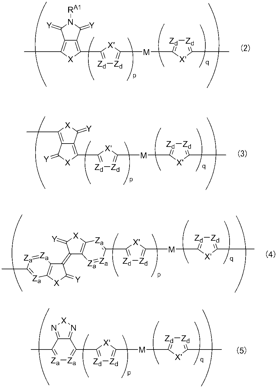
- 有機半導体化合物である、請求項9~11のいずれか1項に記載の化合物。
- 式1で表される構成繰り返し単位を有する、分子量2,000以上の化合物と、
溶媒と、を含むことを特徴とする
有機半導体組成物。


- 下記式I-1で表される構成単位を含む絶縁性ポリマーを更に含有する、請求項13に記載の有機半導体組成物。

- 式1で表される構成繰り返し単位を有する、分子量2,000以上の化合物を含むことを特徴とする
有機半導体膜。


- 下記式I-1で表される構成単位を含む絶縁性ポリマーを更に含有する、請求項15に記載の有機半導体膜。

- 請求項13又は14に記載の有機半導体組成物を基板上に塗布する塗布工程を含む、有機半導体膜の製造方法。
- 請求項14に記載の有機半導体組成物を、表面エネルギーが50~75mNm-1以下であるゲート絶縁膜上に塗布する塗布工程を含む、有機半導体膜の製造方法。
- 請求項13又は14に記載の有機半導体組成物を基板上に塗布する塗布工程を含む、有機半導体素子の製造方法。
- 請求項14に記載の有機半導体組成物を、表面エネルギーが50~75mNm-1以下であるゲート絶縁膜上に塗布する塗布工程を含む、有機半導体素子の製造方法。
Priority Applications (5)
| Application Number | Priority Date | Filing Date | Title |
|---|---|---|---|
| EP16764998.7A EP3258513B1 (en) | 2015-03-16 | 2016-03-16 | Organic semiconductor element, manufacturing method thereof, compound, organic semiconductor composition, organic semiconductor film, and manufacturing method thereof |
| KR1020177026146A KR20170113671A (ko) | 2015-03-16 | 2016-03-16 | 유기 반도체 소자 및 그 제조 방법, 화합물, 유기 반도체 조성물과, 유기 반도체막 및 그 제조 방법 |
| JP2017506576A JP6285075B2 (ja) | 2015-03-16 | 2016-03-16 | 有機半導体素子及びその製造方法、化合物、有機半導体組成物、並びに、有機半導体膜及びその製造方法 |
| CN201680014948.XA CN107431125B (zh) | 2015-03-16 | 2016-03-16 | 有机半导体元件及其制造方法、化合物、有机半导体组合物和有机半导体膜及其制造方法 |
| US15/696,194 US10312447B2 (en) | 2015-03-16 | 2017-09-06 | Organic semiconductor element, manufacturing method thereof, compound, organic semiconductor composition, organic semiconductor film, and manufacturing method thereof |
Applications Claiming Priority (2)
| Application Number | Priority Date | Filing Date | Title |
|---|---|---|---|
| JP2015-051881 | 2015-03-16 | ||
| JP2015051881 | 2015-03-16 |
Related Child Applications (1)
| Application Number | Title | Priority Date | Filing Date |
|---|---|---|---|
| US15/696,194 Continuation US10312447B2 (en) | 2015-03-16 | 2017-09-06 | Organic semiconductor element, manufacturing method thereof, compound, organic semiconductor composition, organic semiconductor film, and manufacturing method thereof |
Publications (1)
| Publication Number | Publication Date |
|---|---|
| WO2016148169A1 true WO2016148169A1 (ja) | 2016-09-22 |
Family
ID=56920050
Family Applications (1)
| Application Number | Title | Priority Date | Filing Date |
|---|---|---|---|
| PCT/JP2016/058256 WO2016148169A1 (ja) | 2015-03-16 | 2016-03-16 | 有機半導体素子及びその製造方法、化合物、有機半導体組成物、並びに、有機半導体膜及びその製造方法 |
Country Status (7)
| Country | Link |
|---|---|
| US (1) | US10312447B2 (ja) |
| EP (1) | EP3258513B1 (ja) |
| JP (1) | JP6285075B2 (ja) |
| KR (1) | KR20170113671A (ja) |
| CN (1) | CN107431125B (ja) |
| TW (1) | TWI688586B (ja) |
| WO (1) | WO2016148169A1 (ja) |
Cited By (4)
| Publication number | Priority date | Publication date | Assignee | Title |
|---|---|---|---|---|
| WO2017038948A1 (ja) * | 2015-09-02 | 2017-03-09 | 富士フイルム株式会社 | 有機薄膜トランジスタ、有機薄膜トランジスタの製造方法、有機半導体組成物、有機半導体膜および有機半導体膜の製造方法 |
| WO2017086320A1 (ja) * | 2015-11-20 | 2017-05-26 | 富士フイルム株式会社 | 有機半導体組成物、有機半導体膜、有機薄膜トランジスタおよび有機薄膜トランジスタの製造方法 |
| WO2017159703A1 (ja) * | 2016-03-16 | 2017-09-21 | 富士フイルム株式会社 | 有機半導体組成物、有機薄膜トランジスタの製造方法、及び有機薄膜トランジスタ |
| WO2019146368A1 (ja) | 2018-01-23 | 2019-08-01 | 富士フイルム株式会社 | 有機半導体素子、有機半導体組成物、有機半導体膜、有機半導体膜の製造方法、及び、これらに用いるポリマー |
Families Citing this family (6)
| Publication number | Priority date | Publication date | Assignee | Title |
|---|---|---|---|---|
| US10622570B2 (en) * | 2016-03-28 | 2020-04-14 | Nippon Steel Chemical & Material Co., Ltd. | Organic electroluminescent element |
| US11183638B2 (en) * | 2018-05-29 | 2021-11-23 | Purdue Research Foundation | Semiconducting polymer blends for high temperature organic electronics |
| KR102554065B1 (ko) * | 2019-03-26 | 2023-07-11 | 도레이 카부시키가이샤 | n형 반도체 소자, n형 반도체 소자의 제조 방법, 무선 통신 장치 및 상품 태그 |
| CN110379924A (zh) * | 2019-06-11 | 2019-10-25 | 北京大学深圳研究生院 | 一种钙钛矿红外光电晶体管及其制备方法 |
| CN110655640B (zh) * | 2019-08-02 | 2022-01-18 | 中国科学院大学 | 一种室温柔性日盲型短波红外聚合物光电探测器及其制备方法 |
| CN110600613B (zh) * | 2019-09-18 | 2022-04-26 | 中国科学院大学 | 一种聚合物光电探测器及其制备方法 |
Citations (6)
| Publication number | Priority date | Publication date | Assignee | Title |
|---|---|---|---|---|
| JP2007335840A (ja) * | 2006-05-18 | 2007-12-27 | Konica Minolta Holdings Inc | 有機薄膜トランジスタの形成方法、及び有機薄膜トランジスタ |
| WO2008044585A1 (en) * | 2006-10-11 | 2008-04-17 | Toray Industries, Inc. | Electron-donating organic material for photovoltaic devices, material for photovoltaic devices, and photovoltaic devices |
| JP2009177136A (ja) * | 2007-12-27 | 2009-08-06 | Sony Corp | 半導体薄膜の形成方法および薄膜半導体装置の製造方法 |
| WO2009139339A1 (ja) * | 2008-05-12 | 2009-11-19 | 東レ株式会社 | カーボンナノチューブ複合体、有機半導体コンポジットならびに電界効果型トランジスタ |
| JP2015038955A (ja) * | 2013-07-19 | 2015-02-26 | 富士フイルム株式会社 | 有機薄膜トランジスタ、有機半導体薄膜および有機半導体材料 |
| WO2015029910A1 (ja) * | 2013-08-30 | 2015-03-05 | 富士フイルム株式会社 | 有機半導体デバイス、これに用いる化合物、組成物及び塗布膜 |
Family Cites Families (6)
| Publication number | Priority date | Publication date | Assignee | Title |
|---|---|---|---|---|
| US7718999B2 (en) * | 2006-12-14 | 2010-05-18 | Xerox Corporation | Polythiophene electronic devices |
| KR101128943B1 (ko) | 2007-04-13 | 2012-03-27 | 주식회사 엘지화학 | 디옥시피롤기를 포함하는 헤테로고리 화합물 및 이를이용한 유기 전자 소자 |
| CA2700713A1 (en) * | 2007-10-09 | 2009-04-16 | Zhimin Hao | Pyrrolopyrrole derivatives, their manufacture and use |
| WO2012147564A1 (ja) * | 2011-04-25 | 2012-11-01 | 住友化学株式会社 | 高分子化合物及びそれを用いた電子素子 |
| KR101589048B1 (ko) * | 2012-12-14 | 2016-01-27 | 경상대학교산학협력단 | 신규한 유기반도체 화합물 및 이를 포함하는 유기전자소자 |
| KR102218245B1 (ko) * | 2014-02-14 | 2021-02-22 | 도요보 가부시키가이샤 | 유기 반도체 재료 |
-
2016
- 2016-03-16 WO PCT/JP2016/058256 patent/WO2016148169A1/ja active Application Filing
- 2016-03-16 JP JP2017506576A patent/JP6285075B2/ja active Active
- 2016-03-16 EP EP16764998.7A patent/EP3258513B1/en active Active
- 2016-03-16 KR KR1020177026146A patent/KR20170113671A/ko not_active Application Discontinuation
- 2016-03-16 TW TW105108021A patent/TWI688586B/zh active
- 2016-03-16 CN CN201680014948.XA patent/CN107431125B/zh active Active
-
2017
- 2017-09-06 US US15/696,194 patent/US10312447B2/en active Active
Patent Citations (6)
| Publication number | Priority date | Publication date | Assignee | Title |
|---|---|---|---|---|
| JP2007335840A (ja) * | 2006-05-18 | 2007-12-27 | Konica Minolta Holdings Inc | 有機薄膜トランジスタの形成方法、及び有機薄膜トランジスタ |
| WO2008044585A1 (en) * | 2006-10-11 | 2008-04-17 | Toray Industries, Inc. | Electron-donating organic material for photovoltaic devices, material for photovoltaic devices, and photovoltaic devices |
| JP2009177136A (ja) * | 2007-12-27 | 2009-08-06 | Sony Corp | 半導体薄膜の形成方法および薄膜半導体装置の製造方法 |
| WO2009139339A1 (ja) * | 2008-05-12 | 2009-11-19 | 東レ株式会社 | カーボンナノチューブ複合体、有機半導体コンポジットならびに電界効果型トランジスタ |
| JP2015038955A (ja) * | 2013-07-19 | 2015-02-26 | 富士フイルム株式会社 | 有機薄膜トランジスタ、有機半導体薄膜および有機半導体材料 |
| WO2015029910A1 (ja) * | 2013-08-30 | 2015-03-05 | 富士フイルム株式会社 | 有機半導体デバイス、これに用いる化合物、組成物及び塗布膜 |
Cited By (6)
| Publication number | Priority date | Publication date | Assignee | Title |
|---|---|---|---|---|
| WO2017038948A1 (ja) * | 2015-09-02 | 2017-03-09 | 富士フイルム株式会社 | 有機薄膜トランジスタ、有機薄膜トランジスタの製造方法、有機半導体組成物、有機半導体膜および有機半導体膜の製造方法 |
| WO2017086320A1 (ja) * | 2015-11-20 | 2017-05-26 | 富士フイルム株式会社 | 有機半導体組成物、有機半導体膜、有機薄膜トランジスタおよび有機薄膜トランジスタの製造方法 |
| JPWO2017086320A1 (ja) * | 2015-11-20 | 2018-08-02 | 富士フイルム株式会社 | 有機半導体組成物、有機半導体膜、有機薄膜トランジスタおよび有機薄膜トランジスタの製造方法 |
| US10902969B2 (en) | 2015-11-20 | 2021-01-26 | Fujifilm Corporation | Organic semiconductor composition, organic semiconductor film, organic thin film transistor, and method of manufacturing organic thin film transistor |
| WO2017159703A1 (ja) * | 2016-03-16 | 2017-09-21 | 富士フイルム株式会社 | 有機半導体組成物、有機薄膜トランジスタの製造方法、及び有機薄膜トランジスタ |
| WO2019146368A1 (ja) | 2018-01-23 | 2019-08-01 | 富士フイルム株式会社 | 有機半導体素子、有機半導体組成物、有機半導体膜、有機半導体膜の製造方法、及び、これらに用いるポリマー |
Also Published As
| Publication number | Publication date |
|---|---|
| JP6285075B2 (ja) | 2018-02-28 |
| TWI688586B (zh) | 2020-03-21 |
| EP3258513A1 (en) | 2017-12-20 |
| US20180006229A1 (en) | 2018-01-04 |
| CN107431125B (zh) | 2020-01-07 |
| US10312447B2 (en) | 2019-06-04 |
| KR20170113671A (ko) | 2017-10-12 |
| EP3258513A4 (en) | 2018-04-25 |
| TW201634520A (zh) | 2016-10-01 |
| JPWO2016148169A1 (ja) | 2017-06-29 |
| EP3258513B1 (en) | 2023-09-13 |
| CN107431125A (zh) | 2017-12-01 |
Similar Documents
| Publication | Publication Date | Title |
|---|---|---|
| JP6285075B2 (ja) | 有機半導体素子及びその製造方法、化合物、有機半導体組成物、並びに、有機半導体膜及びその製造方法 | |
| US10971686B2 (en) | Organic semiconductor element, polymer, organic semiconductor composition, and organic semiconductor film | |
| JP6666996B2 (ja) | 有機薄膜トランジスタ素子、有機半導体膜形成用組成物、有機半導体膜の製造方法及び有機半導体膜 | |
| WO2018061821A1 (ja) | 有機半導体膜形成用組成物、有機半導体膜及びその製造方法、並びに、有機半導体素子 | |
| JP6651606B2 (ja) | 有機半導体組成物、有機薄膜トランジスタの製造方法、及び有機薄膜トランジスタ | |
| JP6469615B2 (ja) | 有機半導体膜形成用組成物、有機半導体膜及びその製造方法、並びに有機半導体素子 | |
| JP6754126B2 (ja) | 有機半導体素子、有機半導体組成物、有機半導体膜の製造方法、有機半導体膜、並びに、これらに用いる化合物及びポリマー | |
| JP6463475B2 (ja) | 有機半導体素子、化合物、有機半導体組成物、および、有機半導体膜の製造方法 | |
| JP6328792B2 (ja) | 有機半導体素子及び化合物 | |
| JP6442057B2 (ja) | 有機半導体素子、化合物、有機半導体組成物、並びに、有機半導体膜及びその製造方法 | |
| JP6328791B2 (ja) | 有機半導体素子及び化合物 | |
| JP6573983B2 (ja) | 有機半導体膜形成用組成物、化合物、有機半導体膜、有機半導体素子 | |
| US11038125B2 (en) | Organic semiconductor element, polymer, organic semiconductor composition, and organic semiconductor film | |
| JP6325128B2 (ja) | 有機半導体素子及び化合物 |
Legal Events
| Date | Code | Title | Description |
|---|---|---|---|
| 121 | Ep: the epo has been informed by wipo that ep was designated in this application |
Ref document number: 16764998 Country of ref document: EP Kind code of ref document: A1 |
|
| ENP | Entry into the national phase |
Ref document number: 2017506576 Country of ref document: JP Kind code of ref document: A |
|
| ENP | Entry into the national phase |
Ref document number: 20177026146 Country of ref document: KR Kind code of ref document: A |
|
| REEP | Request for entry into the european phase |
Ref document number: 2016764998 Country of ref document: EP |
|
| NENP | Non-entry into the national phase |
Ref country code: DE |