WO2016147316A1 - 半導体装置およびその製造方法 - Google Patents
半導体装置およびその製造方法 Download PDFInfo
- Publication number
- WO2016147316A1 WO2016147316A1 PCT/JP2015/057897 JP2015057897W WO2016147316A1 WO 2016147316 A1 WO2016147316 A1 WO 2016147316A1 JP 2015057897 W JP2015057897 W JP 2015057897W WO 2016147316 A1 WO2016147316 A1 WO 2016147316A1
- Authority
- WO
- WIPO (PCT)
- Prior art keywords
- region
- gate electrode
- film
- metal
- silicide layer
- Prior art date
- Legal status (The legal status is an assumption and is not a legal conclusion. Google has not performed a legal analysis and makes no representation as to the accuracy of the status listed.)
- Ceased
Links
Images






Classifications
-
- H—ELECTRICITY
- H10—SEMICONDUCTOR DEVICES; ELECTRIC SOLID-STATE DEVICES NOT OTHERWISE PROVIDED FOR
- H10B—ELECTRONIC MEMORY DEVICES
- H10B43/00—EEPROM devices comprising charge-trapping gate insulators
-
- H—ELECTRICITY
- H10—SEMICONDUCTOR DEVICES; ELECTRIC SOLID-STATE DEVICES NOT OTHERWISE PROVIDED FOR
- H10B—ELECTRONIC MEMORY DEVICES
- H10B43/00—EEPROM devices comprising charge-trapping gate insulators
- H10B43/30—EEPROM devices comprising charge-trapping gate insulators characterised by the memory core region
- H10B43/35—EEPROM devices comprising charge-trapping gate insulators characterised by the memory core region with cell select transistors, e.g. NAND
-
- H—ELECTRICITY
- H10—SEMICONDUCTOR DEVICES; ELECTRIC SOLID-STATE DEVICES NOT OTHERWISE PROVIDED FOR
- H10B—ELECTRONIC MEMORY DEVICES
- H10B43/00—EEPROM devices comprising charge-trapping gate insulators
- H10B43/40—EEPROM devices comprising charge-trapping gate insulators characterised by the peripheral circuit region
-
- H—ELECTRICITY
- H10—SEMICONDUCTOR DEVICES; ELECTRIC SOLID-STATE DEVICES NOT OTHERWISE PROVIDED FOR
- H10D—INORGANIC ELECTRIC SEMICONDUCTOR DEVICES
- H10D30/00—Field-effect transistors [FET]
- H10D30/01—Manufacture or treatment
- H10D30/021—Manufacture or treatment of FETs having insulated gates [IGFET]
- H10D30/0212—Manufacture or treatment of FETs having insulated gates [IGFET] using self-aligned silicidation
- H10D30/0213—Manufacture or treatment of FETs having insulated gates [IGFET] using self-aligned silicidation providing different silicide thicknesses on gate electrodes and on source regions or drain regions
-
- H—ELECTRICITY
- H10—SEMICONDUCTOR DEVICES; ELECTRIC SOLID-STATE DEVICES NOT OTHERWISE PROVIDED FOR
- H10D—INORGANIC ELECTRIC SEMICONDUCTOR DEVICES
- H10D30/00—Field-effect transistors [FET]
- H10D30/60—Insulated-gate field-effect transistors [IGFET]
-
- H—ELECTRICITY
- H10—SEMICONDUCTOR DEVICES; ELECTRIC SOLID-STATE DEVICES NOT OTHERWISE PROVIDED FOR
- H10D—INORGANIC ELECTRIC SEMICONDUCTOR DEVICES
- H10D30/00—Field-effect transistors [FET]
- H10D30/60—Insulated-gate field-effect transistors [IGFET]
- H10D30/601—Insulated-gate field-effect transistors [IGFET] having lightly-doped drain or source extensions, e.g. LDD IGFETs or DDD IGFETs
-
- H—ELECTRICITY
- H10—SEMICONDUCTOR DEVICES; ELECTRIC SOLID-STATE DEVICES NOT OTHERWISE PROVIDED FOR
- H10D—INORGANIC ELECTRIC SEMICONDUCTOR DEVICES
- H10D30/00—Field-effect transistors [FET]
- H10D30/60—Insulated-gate field-effect transistors [IGFET]
- H10D30/69—IGFETs having charge trapping gate insulators, e.g. MNOS transistors
-
- H—ELECTRICITY
- H10—SEMICONDUCTOR DEVICES; ELECTRIC SOLID-STATE DEVICES NOT OTHERWISE PROVIDED FOR
- H10D—INORGANIC ELECTRIC SEMICONDUCTOR DEVICES
- H10D64/00—Electrodes of devices having potential barriers
- H10D64/01—Manufacture or treatment
- H10D64/013—Manufacture or treatment of electrodes having a conductor capacitively coupled to a semiconductor by an insulator
- H10D64/01302—Manufacture or treatment of electrodes having a conductor capacitively coupled to a semiconductor by an insulator the insulator being formed after the semiconductor body, the semiconductor being silicon
- H10D64/01304—Manufacture or treatment of electrodes having a conductor capacitively coupled to a semiconductor by an insulator the insulator being formed after the semiconductor body, the semiconductor being silicon characterised by the conductor
- H10D64/01306—Manufacture or treatment of electrodes having a conductor capacitively coupled to a semiconductor by an insulator the insulator being formed after the semiconductor body, the semiconductor being silicon characterised by the conductor the conductor comprising a layer of silicon contacting the insulator, e.g. polysilicon
- H10D64/01308—Manufacture or treatment of electrodes having a conductor capacitively coupled to a semiconductor by an insulator the insulator being formed after the semiconductor body, the semiconductor being silicon characterised by the conductor the conductor comprising a layer of silicon contacting the insulator, e.g. polysilicon the conductor further comprising a non-elemental silicon additional conductive layer, e.g. a metal silicide layer formed by the reaction of silicon with an implanted metal
- H10D64/0131—Manufacture or treatment of electrodes having a conductor capacitively coupled to a semiconductor by an insulator the insulator being formed after the semiconductor body, the semiconductor being silicon characterised by the conductor the conductor comprising a layer of silicon contacting the insulator, e.g. polysilicon the conductor further comprising a non-elemental silicon additional conductive layer, e.g. a metal silicide layer formed by the reaction of silicon with an implanted metal the additional conductive layer comprising a silicide layer formed by the silicidation reaction between the layer of silicon with a metal layer which is not formed by metal implantation
-
- H—ELECTRICITY
- H10—SEMICONDUCTOR DEVICES; ELECTRIC SOLID-STATE DEVICES NOT OTHERWISE PROVIDED FOR
- H10D—INORGANIC ELECTRIC SEMICONDUCTOR DEVICES
- H10D64/00—Electrodes of devices having potential barriers
- H10D64/01—Manufacture or treatment
- H10D64/017—Manufacture or treatment using dummy gates in processes wherein at least parts of the final gates are self-aligned to the dummy gates, i.e. replacement gate processes
-
- H—ELECTRICITY
- H10—SEMICONDUCTOR DEVICES; ELECTRIC SOLID-STATE DEVICES NOT OTHERWISE PROVIDED FOR
- H10D—INORGANIC ELECTRIC SEMICONDUCTOR DEVICES
- H10D64/00—Electrodes of devices having potential barriers
- H10D64/60—Electrodes characterised by their materials
- H10D64/62—Electrodes ohmically coupled to a semiconductor
-
- H—ELECTRICITY
- H10—SEMICONDUCTOR DEVICES; ELECTRIC SOLID-STATE DEVICES NOT OTHERWISE PROVIDED FOR
- H10D—INORGANIC ELECTRIC SEMICONDUCTOR DEVICES
- H10D64/00—Electrodes of devices having potential barriers
- H10D64/60—Electrodes characterised by their materials
- H10D64/66—Electrodes having a conductor capacitively coupled to a semiconductor by an insulator, e.g. MIS electrodes
- H10D64/661—Electrodes having a conductor capacitively coupled to a semiconductor by an insulator, e.g. MIS electrodes the conductor comprising a layer of silicon contacting the insulator, e.g. polysilicon having vertical doping variation
- H10D64/662—Electrodes having a conductor capacitively coupled to a semiconductor by an insulator, e.g. MIS electrodes the conductor comprising a layer of silicon contacting the insulator, e.g. polysilicon having vertical doping variation the conductor further comprising additional layers, e.g. multiple silicon layers having different crystal structures
- H10D64/663—Electrodes having a conductor capacitively coupled to a semiconductor by an insulator, e.g. MIS electrodes the conductor comprising a layer of silicon contacting the insulator, e.g. polysilicon having vertical doping variation the conductor further comprising additional layers, e.g. multiple silicon layers having different crystal structures the additional layers comprising a silicide layer contacting the layer of silicon, e.g. polycide gates
-
- H—ELECTRICITY
- H10—SEMICONDUCTOR DEVICES; ELECTRIC SOLID-STATE DEVICES NOT OTHERWISE PROVIDED FOR
- H10D—INORGANIC ELECTRIC SEMICONDUCTOR DEVICES
- H10D64/00—Electrodes of devices having potential barriers
- H10D64/60—Electrodes characterised by their materials
- H10D64/66—Electrodes having a conductor capacitively coupled to a semiconductor by an insulator, e.g. MIS electrodes
- H10D64/68—Electrodes having a conductor capacitively coupled to a semiconductor by an insulator, e.g. MIS electrodes characterised by the insulator, e.g. by the gate insulator
- H10D64/691—Electrodes having a conductor capacitively coupled to a semiconductor by an insulator, e.g. MIS electrodes characterised by the insulator, e.g. by the gate insulator comprising metallic compounds, e.g. metal oxides or metal silicates
-
- H—ELECTRICITY
- H10—SEMICONDUCTOR DEVICES; ELECTRIC SOLID-STATE DEVICES NOT OTHERWISE PROVIDED FOR
- H10D—INORGANIC ELECTRIC SEMICONDUCTOR DEVICES
- H10D64/00—Electrodes of devices having potential barriers
- H10D64/60—Electrodes characterised by their materials
- H10D64/66—Electrodes having a conductor capacitively coupled to a semiconductor by an insulator, e.g. MIS electrodes
- H10D64/667—Electrodes having a conductor capacitively coupled to a semiconductor by an insulator, e.g. MIS electrodes the conductor comprising a layer of alloy material, compound material or organic material contacting the insulator, e.g. TiN workfunction layers
Definitions
- the present invention relates to a semiconductor device and a manufacturing method thereof, and can be suitably applied to, for example, a semiconductor device having a nonvolatile memory and a manufacturing method thereof.
- MONOS Metal Oxide Nitride Oxide Semiconductor
- transistors including a metal gate electrode and a high dielectric constant film (high-k film) are used in the logic part.
- This transistor is formed by forming a source region and a drain region using a dummy gate electrode made of a polycrystalline silicon film formed on a substrate and then replacing the dummy gate electrode with a metal gate electrode. The process is known.
- the gate last process after forming silicide layers on the source region and drain region of various MISFETs, the element is covered with an interlayer insulating film, and then the upper surface of the interlayer insulating film is polished to expose the upper surface of the gate electrode. For this reason, when a silicide layer is formed on a gate electrode that constitutes a memory cell and is formed of a semiconductor film, it is necessary to form the silicide layer again after the polishing step.
- Patent Document 1 Japanese Patent Laid-Open No. 2014-154790
- a silicide layer on the source / drain region of the MISFET is formed, and subsequently a gate last process. Describes forming a silicide layer on the gate electrode of the memory cell after forming the metal gate electrode of the MISFET. Further, a full silicide gate electrode is known as a technique replacing the metal gate electrode.
- Patent Document 2 Japanese Patent Application Laid-Open No. 2007-335834
- the n-type FET has an aluminum layer on the gate insulating film.
- a gate electrode made of nickel silicide having a higher nickel content than a silicon content is provided.
- the p-type FET is provided with a gate electrode made of nickel silicide having a nickel content higher than the silicon content on the gate insulating film.
- silicide layers are provided on the surfaces of the source / drain regions of the n-type FET and the p-type FET.
- a gate electrode of a MISFET of a logic part is formed using a gate last process. That is, after the first silicide layer is formed on the source / drain regions of the MISFET of the memory cell and the logic part, and the metal gate electrode of the MISFET of the logic part is formed, the second silicide layer is formed on the gate electrode of the MISFET of the memory cell.
- the first silicide layer and the second silicide layer have the same composition.
- the problem of the present application is to ensure the reliability of the semiconductor device. Another object is to improve the performance of the semiconductor device.
- the MISFET has a gate electrode formed on the semiconductor substrate via a gate insulating film, and a source region and a drain region formed in the semiconductor substrate so as to sandwich the gate electrode.
- a first silicide layer is formed on the surface of the source region and the drain region, and a second silicide layer is formed on the surface of the gate electrode.
- the first silicide layer and the second silicide layer are composed of a first metal and silicon, and include a second metal different from the first metal. The concentration of the second metal in the second silicide layer is lower than the concentration of the second metal in the first silicide layer.
- the reliability performance of the semiconductor device can be ensured.
- the performance of the semiconductor device can be improved.
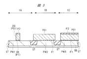
- FIG. 3 is a fragmentary cross-sectional view of the semiconductor device during a manufacturing step following that of FIG. 2;
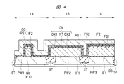
- FIG. 4 is a fragmentary cross-sectional view of the semiconductor device during a manufacturing step following that of FIG. 3;
- FIG. 5 is a fragmentary cross-sectional view of the semiconductor device during a manufacturing step following that of FIG. 4;
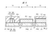
- 6 is a fragmentary cross-sectional view of the semiconductor device during a manufacturing step following that of FIG. 5;
- FIG. FIG. 7 is an essential part cross sectional view of the semiconductor device during a manufacturing step following FIG. 6;
- FIG. 3 is a fragmentary cross-sectional view of the semiconductor device during a manufacturing step following that of FIG. 2;
- FIG. 4 is a fragmentary cross-sectional view of the semiconductor device during a manufacturing step following that of FIG. 3;
- FIG. 5 is a fragmentary cross-sectional view of the semiconductor device during a manufacturing step following that of FIG. 4;
- 6 is a fragmentary cross-sectional
- FIG. 8 is a fragmentary cross-sectional view of the semiconductor device during a manufacturing step following that of FIG. 7;
- FIG. 9 is an essential part cross sectional view of the semiconductor device during a manufacturing step following FIG. 8;
- FIG. 10 is an essential part cross sectional view of the semiconductor device during a manufacturing step following FIG. 9;
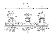
- FIG. 11 is an essential part cross sectional view of the semiconductor device during a manufacturing step following FIG. 10;
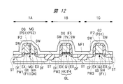
- FIG. 12 is a fragmentary cross-sectional view of the semiconductor device during a manufacturing step following that of FIG. 11;
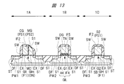
- FIG. 13 is a fragmentary cross-sectional view of the semiconductor device during a manufacturing step following that of FIG. 12;
- FIG. 14 is an essential part cross sectional view of the semiconductor device during a manufacturing step following FIG. 13;
- FIG. 13 is an essential part cross sectional view of the semiconductor device during a manufacturing step following FIG. 13;
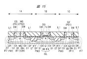
- FIG. 15 is an essential part cross sectional view of the semiconductor device during a manufacturing step following FIG. 14;
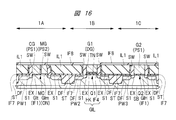
- FIG. 16 is a fragmentary cross-sectional view of the semiconductor device during a manufacturing step following that of FIG. 15;
- FIG. 17 is an essential part cross sectional view of the semiconductor device during a manufacturing step following FIG. 16;
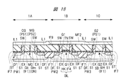
- FIG. 18 is a fragmentary cross-sectional view of the semiconductor device during a manufacturing step following that of FIG. 17;
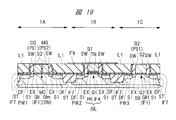
- FIG. 19 is an essential part cross sectional view of the semiconductor device during a manufacturing step following FIG. 18;
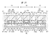
- FIG. 20 is an essential part cross sectional view of the semiconductor device during a manufacturing step following FIG. 19;
- ⁇ ” and + ⁇ represent the relative concentrations of impurities of n-type or p-type conductivity.
- impurity concentration increases in order.
- the semiconductor device (semiconductor integrated circuit device) of the present embodiment is a semiconductor device including a nonvolatile memory (nonvolatile memory element, flash memory), for example, a microcomputer.
- the microcomputer includes a CPU (Central Processing Unit), a RAM (Random Access Memory), an EEPROM (Electrically Erasable Programmable Read Only Memory), a flash memory, an I / O (Input / Output) circuit, and the like.
- the CPU is configured with a low voltage (for example, 5 V or less) drive and a low threshold low voltage MISFET (MISFET: Metal ⁇ ⁇ Insulator Semiconductor Field Effect Transistor) because there is a demand for high speed operation and low power consumption.
- MISFET Metal ⁇ ⁇ Insulator Semiconductor Field Effect Transistor
- the EEPROM or flash memory has a plurality of nonvolatile memory cells arranged in a matrix and a control circuit that performs writing, erasing, reading, and the like on the nonvolatile memory cells.
- a high voltage MISFET that operates at a high voltage (for example, 10 V or more) is included in the control circuit in order to apply a high voltage to the nonvolatile memory cell.
- the nonvolatile memory will be described based on a memory cell based on an n-channel MISFET, but may be a p-channel MISFET.
- the CPU and the control circuit are composed of an n-channel MISFET and a p-channel MISFET.
- the n-channel MISFET will be described as an example.
- FIG. 1 is a cross-sectional view of a main part of the semiconductor device of the present embodiment.
- a memory cell region 1A is shown on the left side, a peripheral circuit region 1B in the center, and a peripheral circuit region 1C on the right side.
- a memory cell MC of a nonvolatile memory is formed in the memory cell region 1A, a low breakdown voltage MISFET (Q1) is formed in the peripheral circuit region 1B, and a high breakdown voltage MISFET (Q2) is formed in the peripheral circuit region 1C.
- symbol part is unclear, a parenthesis is attached
- the semiconductor device is formed on the main surface of the semiconductor substrate SB.
- the semiconductor substrate SB is a semiconductor wafer made of p-type single crystal silicon having a specific resistance of about 1 to 10 ⁇ cm, for example.
- the channel direction of the p-channel type MISFET (the direction connecting the source region and the drain region) is set to ⁇ 110> on the (100) plane of the single crystal silicon substrate. ⁇ 100>.
- the channel direction (direction connecting the source region and the drain region) of the n-channel type MISFET is also set to ⁇ 110> or ⁇ 100>.
- the semiconductor device has an active region and an element isolation region ST formed on the main surface of the semiconductor substrate SB.
- the element isolation region ST is for isolating elements (memory cells) formed in the active region, and an element isolation film made of a silicon oxide film or the like is formed in the element isolation region ST.
- the active region is surrounded by the element isolation region ST, and is defined, that is, partitioned by the element isolation region ST.
- a plurality of active regions exist in the memory cell region 1A, and the plurality of active regions are electrically isolated by the element isolation region ST.
- a p-type well PW1 having a p-type conductivity in which a plurality of memory cells MC are arranged is formed in the memory cell region 1A.
- the memory cell MC is a split gate type memory cell. That is, as shown in FIG. 1, the memory cell MC is formed in the p-type well PW1, and has a control gate electrode CG and a memory gate electrode MG.
- the memory cell MC includes an n type extension region (n ⁇ type semiconductor region, low concentration region, impurity diffusion region) EX, an n type diffusion region (n + type semiconductor region, high concentration region, impurity diffusion region) DF, And a control gate electrode CG and a memory gate electrode MG.
- the n-type extension region EX and the n-type diffusion region DF have an n-type conductivity type that is a conductivity type opposite to the p-type conductivity type.
- the memory cell MC has a silicide layer (gate silicide layer) S2 formed on the upper surface of the control gate electrode CG and the upper surface of the memory gate electrode MG, and a silicide layer (on the upper surface of the diffusion region DF ( SD silicide layer) S1.
- the memory cell MC includes a gate insulating film GIt formed between the control gate electrode CG and the semiconductor substrate SB (or p-type well PW1), the memory gate electrode MG, and the semiconductor substrate SB (or p-type well). PW1) and a gate insulating film GIm formed between the memory gate electrode MG and the control gate electrode CG.
- the control gate electrode CG and the memory gate electrode MG extend along the main surface of the semiconductor substrate SB and are arranged side by side with the gate insulating film GIm interposed between the side surfaces facing each other, that is, the side walls. ing.
- the extending direction of the control gate electrode CG and the memory gate electrode MG is a direction perpendicular to the paper surface of FIG.
- the control gate electrodes CG are commonly and integrally configured.
- the memory gate electrode MG is commonly and integrally configured in a plurality (for example, several tens to several hundreds) of memory cells MC. That is, it is important to reduce the resistance of the control gate electrode CG and the memory gate electrode MG for high-speed operation of the nonvolatile memory.
- the control gate electrode CG and the memory gate electrode MG are adjacent to each other with a gate insulating film GIm interposed therebetween, and the memory gate electrode MG is formed on the side surface of the control gate electrode CG, that is, on the side wall.
- a sidewall spacer is formed through the film GIm.
- the gate insulating film GIm extends over both the region between the memory gate electrode MG and the semiconductor substrate SB and the region between the memory gate electrode MG and the control gate electrode CG.
- the gate insulating film GIt is made of an insulating film IF1.
- the insulating film IF1 is made of a silicon oxide film, a silicon nitride film or a silicon oxynitride film, or a high dielectric constant film having a higher relative dielectric constant than a silicon nitride film, a so-called High-k film.
- a high-k film or a high dielectric constant film means a film having a dielectric constant (relative dielectric constant) higher than that of a silicon nitride film.
- a metal oxide film such as a hafnium oxide film, a zirconium oxide film, an aluminum oxide film, a tantalum oxide film, or a lanthanum oxide film can be used.
- the gate insulating film GIm is made of an insulating film ON.
- the insulating film ON is formed of a stacked film including a silicon oxide film OX1, a silicon nitride film NT formed on the silicon oxide film OX1, and a silicon oxide film OX2 on the silicon nitride film NT.
- the gate insulating film GIm between the memory gate electrode MG and the control gate electrode CG functions as an insulating film for insulating, that is, electrically separating, the memory gate electrode MG and the control gate electrode CG. Therefore, the insulating film between the memory gate electrode MG and the control gate electrode CG can be a separate or different insulating film from the insulating film between the memory gate electrode MG and the semiconductor substrate SB.
- the silicon nitride film NT is an insulating film for accumulating charges and functions as a charge accumulating portion. That is, the silicon nitride film NT is a trapping insulating film formed in the insulating film ON. For this reason, the insulating film ON can be regarded as an insulating film having a charge storage portion therein.
- the silicon oxide film OX1 and the silicon oxide film OX2 positioned above and below the silicon nitride film NT can function as a charge blocking layer that confines charges. That is, the structure in which the silicon nitride film NT is sandwiched between the silicon oxide film OX1 and the silicon oxide film OX2 prevents leakage of charges accumulated in the silicon nitride film NT.
- the control gate electrode CG is made of a silicon film PS1.
- the silicon film PS1 is made of silicon, for example, an n-type polysilicon film which is a polycrystalline silicon film into which an n-type impurity is introduced.
- the control gate electrode CG is made of a patterned silicon film PS1.
- a silicide layer S2 is formed on the upper surface of the silicon film PS1 constituting the control gate electrode CG. Similarly to the control gate electrode CG, the silicide layer S2 also extends in a direction perpendicular to the paper surface of FIG.
- the memory gate electrode MG is made of a silicon film PS2.
- the silicon film PS2 is made of silicon, for example, a p-type polysilicon film that is a polycrystalline silicon film into which p-type impurities are introduced.
- the memory gate electrode MG is formed in a side wall spacer shape on the one side wall of the control gate electrode CG adjacent to the memory gate electrode MG via the gate insulating film GIm.
- a silicide layer S2 is formed on the upper surface of the silicon film PS2 constituting the memory gate electrode MG. Similarly to the memory gate electrode MG, the silicide layer S2 also extends in a direction perpendicular to the paper surface of FIG.
- control gate electrode CG and the silicide layer S2 are shown separately, but the silicide layer S2 may also be referred to as a control gate electrode. The same applies to the memory gate electrode MG and the silicide layer S2.
- the silicide layer S2 formed on the upper surfaces of the control gate electrode CG and the memory gate electrode MG is an alloy layer of nickel (Ni) and silicon (Si) containing platinum (Pt) as an additive.
- the platinum content (content rate) is preferably less than 5% (including 0%).
- the extension region EX and the diffusion region DF are semiconductor regions that function as a source region or a drain region.
- Each of the extension region EX and the diffusion region DF includes a semiconductor region into which an n-type impurity is introduced, and both constitute an LDD (Lightly doped drain) structure.
- the diffusion region DF is higher in concentration than the extension region EX and has a deep junction depth with the well region PW1.
- the pair of extension regions EX and diffusion regions DF are arranged at both ends of the control gate electrode CG and the memory gate electrode MG so as to sandwich the control gate electrode CG and the memory gate electrode MG.
- the extension region EX is arranged between one diffusion region DF and the control gate electrode CG and between the other diffusion region DF and the memory gate electrode MG.
- a silicide layer S1 is formed on the diffusion region DF, that is, on the upper surface (surface) of the diffusion region DF.
- the silicide layer S1 formed on the upper surface of the diffusion region DF is an alloy layer of nickel (Ni) and silicon (Si) containing platinum (Pt) as an additive.
- the content (content ratio) of platinum (Pt) is 5% or more (more preferably 5% or more and 10% or less).
- the extension region EX, the diffusion region DF, and the silicide layer S1 may be expressed as a source region or a drain region.
- the silicide layers S1 and S2 may be a cobalt silicide layer containing an additive instead of a nickel silicide layer containing an additive, and the additive may be aluminum (Al) or carbon (C).
- Side wall spacers SW made of an insulating film such as a silicon oxide film, a silicon nitride film, or a laminated film thereof are formed on the side walls of the control gate electrode CG and the memory gate electrode MG.
- the semiconductor device has an active region and an element isolation region ST formed on the main surface of the semiconductor substrate SB.
- the structure and function of the element isolation region ST are as described above.
- the active region is defined, that is, partitioned by the element isolation region ST, and is electrically isolated from other active regions in the peripheral circuit region 1B by the element isolation region ST.
- the active region has a p-type conductivity type.
- a p-type well PW2 is formed.
- the p-type well PW1 in the memory region 1A is surrounded by an n-type well (not shown) and is electrically isolated from the p-type well PW2. That is, a potential different from that of the p-type well PW2 can be applied to the p-type well PW1.
- the low-breakdown-voltage MISFET (Q1) formed in the peripheral circuit region 1B is formed in the p-type well PW2, and becomes an n-type that serves as a gate electrode G1 and a source region or a drain region. And an extension region (n ⁇ type semiconductor region, low concentration region, impurity diffusion region) EX and an n type diffusion region (n + type semiconductor region, high concentration region, impurity diffusion region) DF. Further, the low breakdown voltage MISFET (Q1) has a silicide layer (SD silicide layer) S1 formed on the upper surface of the diffusion region DF.
- SD silicide layer silicide layer
- the silicide layer (SD silicide layer) S1 has the same composition as the silicide layer S1 formed in the source region and drain region of the memory cell MC. However, the silicide layer S2 is not provided on the upper surface of the gate electrode G1. Further, the low breakdown voltage MISFET (Q1) has a gate insulating film GIL formed between the gate electrode G1 and the semiconductor substrate SB (or p-type well PW2).
- the gate insulating film GIL has a laminated structure of an insulating film IF4 and an insulating film HK formed on the insulating film IF4.
- the insulating film IF4 is, for example, a silicon oxide film
- the insulating film HK is an insulating material film having a higher dielectric constant (relative dielectric constant) than both silicon oxide and silicon nitride, a so-called high-k film (high dielectric constant film). It is.
- a metal oxide film such as a hafnium oxide (HfO) film, a zirconium oxide (ZrO) film, an aluminum oxide (AlO) film, a tantalum oxide (TaO) film, or a lanthanum oxide (LaO) film is used.
- hafnium oxide (HfO) is a film containing hafnium (Hf) and oxygen (O), and the composition ratio is not particularly limited.
- hafnium oxide (ZrO) film, an aluminum oxide (AlO) film, a tantalum oxide (TaO) film, or a lanthanum oxide (LaO) film is used as the insulating film HK.
- hafnium oxide (HfO) is a film containing hafnium (Hf) and oxygen (O)
- the composition ratio is not particularly limited.
- a gate electrode G1 is formed via a metal film TN.
- the metal film TN is a film for adjusting the threshold voltage of the low breakdown voltage MISFET (Q1).
- the metal film TN for example, a titanium nitride (TiN) film, a tantalum nitride (TaN) film, a tungsten nitride (WN) film, a titanium carbide (TiC) film, a tantalum carbide (TaC) film, a tungsten carbide (WC) film,
- a tantalum nitride nitride (TaCN) film, a titanium (Ti) film, a tantalum (Ta) film, a titanium aluminum (TiAl) film, an aluminum (Al) film, or the like can be used.
- the gate electrode G1 is made of a metal film.
- the metal film refers to a conductive film showing metal conduction, and includes not only a single metal film (pure metal film) or an alloy film but also a metal compound film showing metal conduction.
- a titanium aluminum (TiAl) film can be selected as the metal film TN
- an aluminum (Al) film can be selected as the gate electrode G1 on the metal film TN.
- the extension region EX and the diffusion region DF are semiconductor regions that function as a source region or a drain region.
- Each of the extension region EX and the diffusion region DF includes a semiconductor region into which an n-type impurity is introduced, and both form an LDD structure.
- the diffusion region DF is higher in concentration than the extension region EX and has a deep junction depth with the well region PW2.
- the pair of extension regions EX and diffusion regions DF are disposed at both ends of the gate electrode G1 so as to sandwich the gate electrode G1.
- an extension region EX is disposed between one diffusion region DF and the gate electrode G1 and between the other diffusion region DF and the gate electrode G1.
- the aforementioned silicide layer S1 is formed on the diffusion region DF, that is, on the upper surface (surface) of the diffusion region DF. Further, a sidewall spacer SW made of an insulating film such as a silicon oxide film, a silicon nitride film, or a laminated film thereof is formed on the side wall of the gate electrode G1.
- the extension region EX, the diffusion region DF, and the silicide layer S1 may be expressed as a source region or a drain region.
- the semiconductor device has an active region and an element isolation region ST formed on the main surface of the semiconductor substrate SB.
- the structure and function of the element isolation region ST are as described above.
- the active region is defined, that is, partitioned by the element isolation region ST, and is electrically isolated from the other active regions in the peripheral circuit region 1C by the element isolation region ST.
- the active region has a p-type conductivity type.
- a p-type well PW3 is formed. As described above, since the p-type well PW1 is surrounded by an n-type well (not shown), it is also electrically isolated from the p-type well PW3. That is, a potential different from that of the p-type well PW3 can be applied to the p-type well PW1.
- the high-breakdown-voltage MISFET (Q2) formed in the peripheral circuit region 1C is formed in the p-type well PW3, and becomes an n-type that serves as a gate electrode G2 and a source region or a drain region. And an extension region (n ⁇ type semiconductor region, low concentration region, impurity diffusion region) EX and an n type diffusion region (n + type semiconductor region, high concentration region, impurity diffusion region) DF. Further, the high voltage MISFET (Q2) has a silicide layer (SD silicide layer) S1 formed on the upper surface of the diffusion region DF, and a silicide layer (gate silicide layer) S2 is formed on the upper surface of the gate electrode G2. Have. The silicide layers S1 and S2 are the same as the silicide layers S1 and S2 described above.
- the high voltage MISFET (Q2) has a gate insulating film GIH formed between the gate electrode G2 and the semiconductor substrate SB (or p-type well PW3).
- the gate length of the gate electrode G2 of the high breakdown voltage MISFET (Q2) is larger (longer) than the gate length of the gate electrode G1 of the low breakdown voltage MISFET (Q1), so that the breakdown voltage between the source region and the drain region is increased. Can be improved.
- the gate length refers to the length of the gate electrode in the direction connecting the source region and the drain region. That is, it is the length of the gate electrode in the horizontal direction of the paper surface of FIG.
- the gate insulating film GIH is made of an insulating film IF1.
- the insulating film IF1 is made of a silicon oxide film, a silicon nitride film, or a silicon oxynitride film, and is preferably thicker than the gate insulating film GIt.
- the insulating film IF1 is preferably thicker in terms of oxide film than the gate insulating film GIL of the low breakdown voltage MISFET (Q1), and preferably at least thicker than the insulating film IF4.
- a gate electrode G2 is disposed on the gate insulating film GIH, and the gate electrode G2 is made of the silicon film PS1 described above. Further, the above-described silicide layer S2 is formed on the upper surface of the gate electrode G2.
- the source region and drain region of the high withstand voltage MISFET (Q2) are the same as the low withstand voltage MISFET (Q1), and have an LDD structure composed of the extension region EX and the diffusion region DF.
- the impurity concentration of the extension region EX of the high breakdown voltage MISFET (Q2) is set to be lower than the impurity concentration of the extension region EX of the low breakdown voltage MISFET (Q1).
- the silicide layer S1 formed on the upper surface of the diffusion region DF of the high breakdown voltage MISFET (Q2) is the same as the silicide layer S1 formed on the upper surface of the diffusion region DF of the low breakdown voltage MISFET (Q1) and the memory cell MC.
- the silicide layer S2 formed on the upper surface of the high breakdown voltage MISFET (Q2) gate electrode G2 is the same as the silicide layer S2 formed on the upper surface of the control gate electrode CG and the memory gate electrode MG of the memory cell MC.
- the channel direction (that is, the direction from the source region to the drain region) of the high breakdown voltage MISFET (Q2) is the ⁇ 110> or ⁇ 100> direction, so that it is formed on the upper surface of the diffusion region DF. Whisker defects in which the silicide layer S1 extends in the channel direction are likely to occur, but the whisker defects can be prevented by including platinum (Pt) in the silicide layer S1.
- a sidewall spacer SW made of an insulating film such as a silicon oxide film, a silicon nitride film, or a laminated film thereof is formed on the sidewall of the gate electrode G2.
- the extension region EX, the diffusion region DF, and the silicide layer S1 may be expressed as a source region or a drain region.
- a laminated film of the film IF7 and the interlayer insulating film IL1 is formed.
- the upper surface of the laminated film of the insulating film IF7 and the interlayer insulating film IL1 has a height substantially equal to the upper surfaces of the control gate electrode CG, the memory gate electrode MG, and the gate electrodes G1 and G2.
- the insulating film IF7 is made of, for example, a silicon nitride film
- the interlayer insulating film IL1 is made of, for example, a silicon oxide film.
- an interlayer insulating film IL2 made of, for example, a silicon oxide film is formed on the interlayer insulating film IL1.
- an insulating film IF9 made of a silicon oxide film is interposed between the interlayer insulating film IL1 and the interlayer insulating film IL2.
- a contact hole exposing a part of silicide layer S1 on the surface of diffusion region DF is formed in insulating film IF7, interlayer insulating film IL1, and interlayer insulating film IL2, for example.
- the conductive contact plug CP is formed in the contact hole.
- the contact plug CP includes a main conductor made of tungsten (W) or the like and a barrier conductor film (for example, a titanium film, a titanium nitride film, or a laminated film thereof).
- the barrier conductor film includes the main conductor and a silicide layer. It is interposed between S1.
- the contact hole also penetrates the insulating film IF9.
- the first wiring layer M1 is disposed on each contact plug CP, and the wiring layer M1 is connected to the silicide layer S1 via the contact plug CP. That is, the wiring layer M1 is electrically connected to the diffusion region DF.
- the wiring layer M1 is made of, for example, a conductor film whose main conductor is aluminum (Al) or copper (Cu).
- the concentration (content) of the additive contained in the silicide layer S1 formed on the upper surface of the diffusion region DF is formed on the upper surfaces of the control gate electrode CG, the memory gate electrode MG, and the gate electrode G2. It is important to make the concentration higher than the concentration (content) of the additive contained in the silicide layer S2.
- concentration of the additive contained in the silicide layer S1 By increasing the concentration of the additive contained in the silicide layer S1, abnormal growth of the silicide layer S1 formed on the upper surface of the diffusion region DF can be prevented, and between the source region or drain region and the well regions PW1, PW2, and PW3. Leakage current can be reduced. That is, it is effective for reducing the power consumption of the semiconductor device.
- the sheet resistance of the silicide layer S2 increases, thereby increasing the resistance of the gate electrode including the silicide layer S2 and performing high-speed operation. Hinder. In the silicide layer having a high concentration of the additive, the crystal grains become finer, so that the probability of grain boundary scattering of current (electrons) flowing through the silicide layer increases. Furthermore, the probability of electron scattering increases due to the inclusion of the additive. These factors are thought to increase the sheet resistance of the silicide layer.
- the crystal grain size of the silicide layer S2 is made larger than the crystal grain size of the silicide layer S1. Can also be larger.
- the sheet resistance of the silicide layer S2 can be reduced. That is, the resistance of the gate electrode of the MISFET is reduced, which is effective for high-speed operation of the MISFET.
- the sheet resistance of the silicide layer S2 can be reduced by reducing the concentration of the additive in the silicide layer S2 below the concentration of the additive in the silicide layer S1.
- the control gate electrode CG or the memory gate electrode MG of the memory cell MC is also used as a common wiring for the plurality of memory cells MC, the length in the gate width direction is formed in the peripheral circuit region 1B. Longer than the low breakdown voltage MISFET (Q1). Therefore, reducing the resistance of the silicide layer S2 on the upper surface of the control gate electrode CG or the memory gate electrode MG is effective for high-speed operation of the nonvolatile memory.
- the concentration of the additive contained in the silicide layers S1 and S2 is, for example, the concentration per unit area of the surface of the silicide layers S1 and S2.
- the relative comparison of the content rate of the 2nd metal (for example, Pt) which is an additive contained in the silicide layers S1 and S2 containing the 1st metal (for example, Ni) and silicon is, for example, energy dispersive X-ray It can be carried out by spectroscopy (EDX: Energy Dispersive X-ray Spectroscopy).
- elemental analysis and composition analysis of the silicide layers S1 and S2 can be performed by detecting characteristic X-rays generated by irradiating the surfaces (upper surfaces) of the silicide layers S1 and S2 with an electron beam and performing spectral analysis with energy.
- control gate electrode CG and the memory gate electrode MG constituting the memory cell MC are composed of a polysilicon film and a silicide layer S2 formed on the surface (upper surface) of the polysilicon film.
- the electrode CG and the memory gate electrode MG are separated by a gate insulating film GIm.
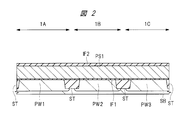
- FIGS. 2 to 20 are cross-sectional views of the semiconductor device according to the present embodiment during the manufacturing process.
- the cross-sectional views of FIGS. 2 to 20 correspond to the cross-sectional view of FIG.
- the memory cell region 1A is shown on the left side, the peripheral circuit region 1B in the center, and the peripheral circuit region 1C on the right side.
- a memory cell MC of a nonvolatile memory is formed in the memory cell region 1A, and a low breakdown voltage MISFET (Q1) and a high breakdown voltage MISFET (Q2) are formed in the peripheral circuit regions 1B and 1C, respectively.
- Q1 low breakdown voltage MISFET
- Q2 high breakdown voltage MISFET
- a semiconductor substrate (semiconductor wafer) SB made of p-type single crystal silicon (Si) or the like is prepared. Then, a plurality of element isolation regions ST that define active regions are formed on the main surface of the semiconductor substrate SB.
- the element isolation region ST is made of an insulator such as silicon oxide and can be formed by, for example, the STI method or the LOCOS method. Here, the formation of the element isolation region by the STI method will be described.
- the silicon nitride film and the silicon oxide film are etched using a photolithography technique and a dry etching method to selectively cover the active region.
- a silicon nitride film and a silicon oxide film thus formed are formed.
- a groove is formed on the upper surface of the semiconductor substrate SB exposed from the patterned silicon nitride film and silicon oxide film. A plurality of the grooves are formed.
- an insulating film made of, for example, silicon oxide is embedded in these trenches, and then each insulating film on the silicon nitride film is removed by a polishing process or the like, thereby forming a plurality of element isolation regions ST.
- the element isolation region ST is formed so as to surround the active region, and is formed between the memory cell region 1A, the peripheral circuit region 1B, and the peripheral circuit region 1C. As a result, the structure shown in FIG. 2 is obtained.
- p-type wells PW1, PW2, and PW3 are formed on the main surface of the semiconductor substrate SB in the memory cell region 1A, the peripheral circuit region 1B, and the peripheral circuit region 1C.
- the p-type wells PW1, PW2, and PW3 can be formed by ion-implanting p-type impurities such as boron (B) into the semiconductor substrate SB.
- the p-type wells PW1, PW2, and PW3 formed in the respective formation regions of the memory cell MC, the high breakdown voltage MISFET (Q2), or the low breakdown voltage MISFET (Q1) can be formed by the same ion implantation process.
- each region can be formed by a different ion implantation process.
- the concentration of the p-type well PW3 in the peripheral circuit region 1C is preferably higher than the concentration of the p-type well PW2 in the peripheral circuit region 1B.
- an insulating film IF1 for a gate insulating film is formed on the main surface of the semiconductor substrate SB. That is, the insulating film IF1 is formed on the upper surface (front surface) of the semiconductor substrate SB in the memory cell region 1A and the peripheral circuit regions 1B and 1C.
- a silicon oxide film can be used as the insulating film IF1.
- the respective insulating films IF1 in the memory cell region 1A and the peripheral circuit regions 1B and 1C may be formed in different steps, so that the film thicknesses are different from each other.
- the insulating film IF1 in the peripheral circuit region 1C is made thicker than the insulating film IF1 in the memory cell region 1A.
- a silicon film PS1 made of a polycrystalline silicon film is formed on the semiconductor substrate SB using, for example, a CVD (Chemical Vapor Deposition) method so as to cover the upper surface of the insulating film IF1.
- the silicon film PS1 can be formed as a low-resistance semiconductor film (doped polysilicon film) by introducing impurities at the time of film formation or by implanting impurities after film formation.
- phosphorus (P) can be suitably used as the n-type impurity introduced into the silicon film PS1, for example, phosphorus (P) can be suitably used.
- an insulating film IF2 is formed on the silicon film PS1 by using, for example, a CVD method.
- the insulating film IF2 is a cap insulating film made of, for example, silicon nitride (SiN).
- the film thickness of the insulating film IF2 can be about 20 to 50 nm, for example.
- the laminated film including the insulating film IF2, the silicon film PS1, and the insulating film IF1 in the memory cell region 1A is patterned by a photolithography technique and an etching technique.
- a stacked body of the gate insulating film GIt made of the insulating film IF1, the control gate electrode CG made of the silicon film PS1, and the cap insulating film made of the insulating film IF2 is formed.
- the control gate electrode CG is a pattern extending in the gate width direction in plan view.
- the gate width direction is the depth direction of the paper surface of FIG.
- the laminated film composed of the insulating film IF2, the silicon film PS1, and the insulating film IF1 is processed between the peripheral circuit regions 1B and 1C using the photolithography technique and the etching technique. That is, between the peripheral circuit regions 1B and 1C, the stacked body including the insulating film IF2, the silicon film PS1, and the insulating film IF1 is separated from each other and includes the insulating film IF2, the silicon film PS1, and the insulating film IF1 in the memory cell region 1A. Separated from the laminate. However, the insulating films IF1 are not necessarily separated from each other.
- the insulating film IF2 in the peripheral circuit region 1B is selectively removed by using a photolithography technique and a wet etching method different from the patterning of the laminated film described above. As a result, the upper surface of the silicon film PS1 in the peripheral circuit region 1B is exposed. At this time, the insulating film IF2 in the memory cell region 1A and the peripheral circuit region 1C is left without being removed. That is, the wet etching step is performed using a resist film (not shown) having a pattern that covers the memory cell region 1A and the peripheral circuit region 1C and exposes the peripheral circuit region 1B as a mask. Remove the resist film.
- the insulating film ON for the gate insulating film GIm is formed on the main surface of the semiconductor substrate SB.
- the insulating film ON covers the upper surface of the semiconductor substrate SB in the memory cell region 1A and the side walls and the upper surface of the stacked body including the gate insulating film GIt, the control gate electrode CG, and the insulating film IF2. Further, the sidewall and upper surface of the multilayer body including the insulating film IF1 and the silicon film PS1 in the peripheral circuit region 1B are covered, and the sidewall and upper surface of the multilayer body including the insulating film IF1, the silicon film PS1, and the insulating film IF2 in the peripheral circuit region 1C are covered. Covering.
- the insulating film ON is an insulating film having a charge storage portion inside.
- the insulating film ON includes a silicon oxide film OX1 formed over the semiconductor substrate SB, a silicon nitride film NT formed over the silicon oxide film OX1, and a silicon oxide formed over the silicon nitride film NT. It consists of a laminated film with film OX2.
- the silicon oxide films OX1 and OX2 can be formed by, for example, an oxidation process (thermal oxidation process), a CVD method, or a combination thereof.
- an oxidation process thermal oxidation process
- CVD method chemical vapor deposition method
- ISSG In-Situ Steam Generation
- the silicon nitride film NT can be formed by, for example, a CVD method.
- a silicon nitride film NT is formed as an insulating film (charge storage layer) that constitutes a memory cell and has a trap level.
- the film used as the charge storage layer is preferably a silicon nitride film in terms of reliability, but is not limited to a silicon nitride film, such as an aluminum oxide film (alumina), a hafnium oxide film, or a tantalum oxide film.
- a high dielectric constant film (high dielectric constant insulating film) having a dielectric constant higher than that of the silicon nitride film can also be used as the charge storage layer or the charge storage portion.
- the thickness of the silicon oxide film OX1 can be, for example, about 2 to 10 nm
- the thickness of the silicon nitride film NT can be, for example, about 5 to 15 nm
- the thickness of the silicon oxide film OX2 can be, for example, 2 to 10 nm. Can be about.
- a polycrystalline silicon film PS2 is formed on the main surface of the semiconductor substrate SB using, for example, a CVD method so as to cover the surface of the insulating film ON.
- the silicon film PS2 is formed on the side wall of the control gate electrode CG via the insulating film ON.
- the film thickness of the silicon film PS2 is 40 nm, for example.
- the silicon film PS2 may be formed as an amorphous silicon film and then changed to the silicon film PS2 made of a polycrystalline silicon film by a subsequent heat treatment.
- the silicon film PS2 is a film into which, for example, a p-type impurity (for example, boron (B)) is introduced at a relatively high concentration.
- the silicon film PS2 is a film for forming the memory gate electrode MG.
- the film thickness refers to the thickness of the film in a direction perpendicular to the main surface of the semiconductor substrate SB.
- the insulating film ON having a three-layered structure of the silicon oxide film OX1, the silicon nitride film NT, and the silicon nitride film NT, but the cross-sectional view used in the following description makes the figure easy to understand. Therefore, illustration of the laminated structure of the insulating film ON is omitted. That is, the insulating film ON has a laminated structure, but in the drawings used in the following description, the insulating film ON is shown as one film GIm.
- the upper surface of the insulating film ON is selectively exposed by etching back (anisotropic dry etching) the silicon film PS2 by anisotropic etching technology.
- the silicon film PS2 is anisotropically etched (etch back), so that the insulating film ON is formed on the sidewalls of the stacked body including the gate insulating film GIt, the control gate electrode CG, and the insulating film IF2. Accordingly, the silicon film PS2 is left in a sidewall shape.
- the memory gate electrode MG made of the silicon film PS2 remaining in a sidewall shape via the insulating film ON is formed on one of the sidewalls of the stacked body. Further, the upper surface of the insulating film ON in the peripheral circuit regions 1B and 1C is exposed by the etch back.
- a portion of the insulating film ON that is exposed without being covered with the memory gate electrode MG is removed by etching (for example, wet etching).
- etching for example, wet etching
- the insulating film ON immediately below the memory gate electrode MG remains without being removed.
- the insulating film ON positioned between the stacked body including the gate insulating film GIt, the control gate electrode CG, and the insulating film IF2 and the memory gate electrode MG remains without being removed.
- the insulating film ON in other regions is removed, the upper surface of the semiconductor substrate SB and the upper surface of the insulating film IF2 in the memory cell region 1A are exposed, and the upper surface of the silicon film PS1 in the peripheral circuit region 1B and the peripheral circuit region 1C.
- the upper surface of the insulating film IF2 is exposed. Further, the side wall of the control gate electrode CG that is not adjacent to the memory gate electrode MG is exposed.
- an insulating film IF3 is formed on the main surface of the semiconductor substrate SB by using, for example, a CVD method.
- the insulating film IF3 is made of, for example, a silicon nitride film.
- the silicon film PS1 in the peripheral circuit region 1B and the silicon film PS1 and the insulating film IF2 in the peripheral circuit region 1C are covered with the insulating film IF3.
- a stacked body including the gate insulating film GIt, the control gate electrode CG, and the insulating film IF2 in the memory cell region 1A, the gate insulating film GIm and the memory gate electrode MG adjacent to the side wall of the stacked body, and the memory cell region 1A
- the main surface of the semiconductor substrate SB is covered with an insulating film IF3.
- the insulating film IF3 may be a stacked film of a silicon oxide film and a silicon nitride film over the silicon oxide film.
- a resist film PR1 that exposes the peripheral circuit region 1C and covers the insulating film IF3 in the memory cell region 1A and the peripheral circuit region 1C is formed.
- the insulating film IF3 in contact with each of the upper surface and the side wall of the silicon film PS1 is exposed from the resist film PR1.
- the insulating film IF3 exposed from the resist film PR1 is removed by a wet etching method, and then the resist film PR1 is removed. As a result, the silicon film PS1 in the peripheral circuit region 1B is exposed.
- the silicon film PS1 and the insulating film IF1 in the peripheral circuit region 1B are removed by, eg, wet etching to expose the main surface of the semiconductor substrate SB.
- the stacked body including the gate insulating film GIt, the control gate electrode CG, and the insulating film IF2 in the memory cell region 1A, and the gate insulating film GIm and the memory gate electrode MG adjacent to the sidewall of the stacked body are separated from the insulating film IF3. Since it is covered with, it is not removed. Further, the insulating film IF2, the silicon film PS1, and the insulating film IF1 in the peripheral circuit region 1C are also not removed because they are covered with the insulating film IF3.
- the insulating films IF4, HK, the metal film TN, the silicon film PS3, and the insulating film IF5 are sequentially formed on the main surface of the semiconductor substrate SB.
- the insulating film IF4 is made of, for example, a silicon oxide film and is formed using an oxidation method such as a thermal oxidation method, the insulating film IF4 is formed only on the main surface of the semiconductor substrate SB in the peripheral circuit region 1B.
- the stacked body including the gate insulating film GIt, the control gate electrode CG, and the insulating film IF2 in the memory cell region 1A, and the gate insulating film GIm and the memory gate electrode MG adjacent to the side wall of the stacked body are separated from the insulating film IF3. , HK, metal film TN, silicon film PS3 and insulating film IF5.
- the laminated body including the insulating film IF1, the silicon film PS1, and the insulating film IF2 in the peripheral circuit region 1C is also covered with the insulating films IF3, HK, the metal film TN, the silicon film PS3, and the insulating film IF5.
- the insulating film HK is an insulating film for a gate insulating film.
- the insulating film IF4 and the insulating film HK are films constituting a gate insulating film of a MISFET (Q1) to be formed later in the peripheral circuit region 1B.
- the insulating film HK is an insulating material film having a higher dielectric constant (relative dielectric constant) than both silicon oxide and silicon nitride, a so-called high-k film (high dielectric constant film).
- a metal oxide film such as a hafnium oxide film, a zirconium oxide film, an aluminum oxide film, a tantalum oxide film, or a lanthanum oxide film can be used, and these metal oxide films are formed of nitrogen (N ) And silicon (Si) or both.
- the insulating film HK can be formed by, for example, an ALD (Atomic layer deposition) method.
- the film thickness of the insulating film HK is, for example, 1.5 nm.
- the insulating film HK is used as the gate insulating film, the physical film thickness of the gate insulating film can be increased as compared with the case where a silicon oxide film is used. Can be obtained.
- the metal film TN is made of, for example, a titanium nitride film, and can be formed by, for example, a sputtering method.
- the silicon film PS3 is made of a polysilicon film and can be formed by, for example, a CVD method.
- the film thickness of the silicon film PS3 is, for example, 40 nm.
- the silicon film PS3 is formed as an amorphous silicon film, and the silicon film PS3 made of an amorphous silicon film can be changed to a silicon film PS3 made of a polycrystalline silicon film by subsequent heat treatment.
- the silicon film PS3 is a film for forming a dummy gate electrode DG described later.
- the insulating film IF5 is a cap insulating film made of, for example, silicon nitride, and can be formed by, for example, a CVD method.
- the insulating film IF4, HK, the metal film TN, the silicon film PS3, and the insulating film IF5 are selectively left in the peripheral circuit region 1B, and from the memory cell region 1A and the peripheral circuit region 1C,
- the insulating films IF3, HK, the metal film TN, the silicon film PS3, and the insulating film IF5 are removed by, for example, a wet etching method.
- a wet etching method the upper surface of the laminated structure including the insulating films IF4 and HK, the metal film TN, the silicon film PS3, and the insulating film IF5 in the peripheral circuit region 1B is selectively covered with an insulating film such as a silicon oxide film. Then, the wet etching is performed using the insulating film as a mask.
- the insulating film IF5, the silicon film PS3, the metal film TN, the insulating films HK and IF4 in the peripheral circuit region 1B, and the insulating film IF2, the silicon film PS1 and the insulating film in the peripheral circuit region 1C are further formed.
- the film IF1 is patterned using a photolithography technique and an etching technique.
- the dummy gate electrode DG made of the silicon film PS3, the metal film TN, the gate insulating film GIL made of the insulating film HK and IF4, which form the MISFET (Q1) are formed in the peripheral circuit region 1B.
- the gate electrode G2 and the gate insulating film GIH constituting the MISFET (Q2) are formed in the peripheral circuit region 1C.
- the insulating film IF5 in the peripheral circuit region 1B and the insulating film IF2 in the peripheral circuit region 1C are patterned using a photolithography technique and an etching method. Thereafter, in the peripheral circuit region 1B, etching is performed using the patterned insulating film IF5 as a hard mask, thereby patterning the silicon film PS3, the metal film TN, the insulating film HK, and IF4 and IF1, whereby the dummy gate electrode DG, A metal film TN and a gate insulating film GIL made of the insulating films HK and IF4 are formed.
- the silicon film PS1 and the insulating film IF1 are patterned by performing etching using the patterned insulating film IF2 as a hard mask, thereby forming the gate electrode G2 and the gate insulating film GIH.
- a plurality of extension regions (n ⁇ type semiconductor regions, impurity diffusion regions) EX are formed using an ion implantation method or the like. That is, n-type impurities such as arsenic (As) or phosphorus (P) are introduced into the surface of the semiconductor substrate SB in the active region, but the control gate electrode CG, the memory gate electrode MG, the dummy gate electrode DG, and the gate Impurities are not introduced below the electrode G2. That is, the extension region EX is formed in the active region on both sides of the control gate electrode CG and the memory gate electrode MG, on both sides of the dummy gate electrode DG, and on both sides of the gate electrode G2.
- n-type impurities such as arsenic (As) or phosphorus (P) are introduced into the surface of the semiconductor substrate SB in the active region, but the control gate electrode CG, the memory gate electrode MG, the dummy gate electrode DG, and the gate Impurities are not introduced below the electrode G2. That is,
- an offset spacer that covers the side walls of the control gate electrode CG, the memory gate electrode MG, the dummy gate electrode DG, and the gate electrode G2, for example, a silicon nitride film, a silicon oxide film, or a laminated film thereof May be formed.
- the extension regions EX of the memory cell region 1A and the peripheral circuit regions 1B and 1C can be formed by the same ion implantation step, but can also be formed by different ion implantation steps.
- a p-type impurity is formed on the main surface of the semiconductor substrate SB in the peripheral circuit region 1B using the insulating film IF5 and the dummy gate electrode DG as a mask.
- the halo region may be formed by implanting (for example, boron (B)). The halo region is located closer to the center of the dummy gate electrode DG than the extension region EX.
- a halo region may be formed at a location close to the channel region of the high voltage MISFET (Q2).
- sidewalls SW made of insulating films are formed to cover the sidewalls on both sides of the structure including the control gate electrode CG and the memory gate electrode MG in the memory cell region 1A.
- sidewalls SW are formed in the peripheral circuit region 1B to cover the sidewalls on both sides of the stacked body made up of the gate insulating film GIL, the metal film TN, the dummy gate electrode DG, and the insulating film IF5.
- the sidewall SW that covers the sidewalls on both sides of the stacked body including the gate insulating film GIH, the gate electrode G2, and the insulating film IF2 is formed.
- the sidewall SW is formed by sequentially forming, for example, a silicon oxide film and a silicon nitride film on the semiconductor substrate SB using a CVD method or the like, and then partially removing the silicon oxide film and the silicon nitride film by anisotropic etching.
- the upper surface of the semiconductor substrate SB and the upper surfaces of the insulating films IF2 and IF5 are exposed.
- the sidewall SW can be selectively formed on the sidewalls of the control gate electrode CG, the memory gate electrode MG, the dummy gate electrode DG, and the gate electrode G2.
- the sidewall SW may be formed of a laminated film, but the interface between the films constituting the laminated film is not shown in the drawing.
- the sidewall SW may be formed of a single layer film such as a silicon oxide film or a silicon nitride film, for example.
- a diffusion region (n + type semiconductor region, impurity diffusion region) DF is formed in the memory cell region 1A and the peripheral circuit regions 1B and 1C using an ion implantation method or the like. That is, n-type impurities such as arsenic (As) or phosphorus (P) are introduced into the surface of the semiconductor substrate SB in the active region, but the control gate electrode CG, memory gate electrode MG, dummy gate electrode DG, gate Impurities are not introduced below the electrode G2 and the sidewall SW.
- n-type impurities such as arsenic (As) or phosphorus (P) are introduced into the surface of the semiconductor substrate SB in the active region, but the control gate electrode CG, memory gate electrode MG, dummy gate electrode DG, gate Impurities are not introduced below the electrode G2 and the sidewall SW.
- the diffusion region DF is formed in the active region on both sides of the control gate electrode CG and the memory gate electrode MG, on both sides of the dummy gate electrode DG, and on both sides of the gate electrode G2, but is formed outside the sidewall SW. .
- the diffusion region DF has a higher impurity concentration and a deep junction depth than the extension region EX.
- a source region and a drain region having an LDD structure including the extension region EX and the diffusion region DF having an impurity concentration higher than that of the extension region EX are formed.
- the extension region EX and the diffusion region DF formed on the upper surface of the semiconductor substrate SB so as to sandwich the control gate electrode CG and the memory gate electrode MG constitute a source region and a drain region of the memory cell MC.
- the extension region EX and the diffusion region DF formed on the upper surface of the semiconductor substrate SB so as to sandwich the dummy gate electrode DG constitute the source region and the drain region of the low breakdown voltage MISFET (Q1).
- the extension region EX and the diffusion region DF formed on the upper surface of the semiconductor substrate SB so as to sandwich the gate electrode G2 constitute a source region and a drain region of the high breakdown voltage MISFET (Q2).
- the diffusion regions DF of the memory cell region 1A and the peripheral circuit regions 1B and 1C can be formed by the same ion implantation step, but can also be formed by different ion implantation steps.
- activation annealing which is a heat treatment for activating impurities introduced into the source and drain semiconductor regions (extension region EX and diffusion region DF), is performed.
- a silicide layer is formed by performing a so-called salicide (Self-Aligned Silicide) process, which will be described with reference to FIGS. 12 and 13.
- the silicide layer can be formed as follows.
- a metal film MF1 for forming a silicide layer is formed (deposited) on the main surface of the semiconductor substrate SB including the upper surface of the diffusion region DF and the upper surface of the memory gate electrode MG.
- the film thickness of the metal film MF1 is, for example, 20 to 25 nm.
- the metal film MF1 can be formed by, for example, a sputtering method using an alloy target in which platinum (Pt) is added to nickel (Ni).
- the content (concentration) of platinum (Pt) that is an additive of the alloy target is 5% or more (more preferably 5% or more and 10% or less).
- the additive may be aluminum (Al) or carbon (C), but the content (concentration) in that case is also 5% or more (more preferably 5% or more and 10% or less).
- platinum has higher heat resistance than aluminum or carbon, it can be suitably used for the alloy film.
- the metal film MF1 formed by sputtering using the alloy target is a nickel (Ni) film containing platinum (Pt), and the content of platinum (Pt) is 5% or more.
- Ni nickel as the main material
- platinum (Pt) as an additive is referred to as a second metal.
- the first heat treatment is performed on the semiconductor substrate SB to cause the surface layer portions of the diffusion region DF and the memory gate electrode MG to react with the metal film MF1.
- This first heat treatment is a heat treatment for causing the metal film MF1 to react with the diffusion region DF and the silicon of the memory gate electrode.
- the upper portion of each of the diffusion region DF and the memory gate electrode MG is formed.
- a silicide layer in which NiSi microcrystals and Ni 2 Si are dominant is formed. At this stage, the silicide layer has a relatively high resistance different from the silicide layer S1 shown in FIG.
- the silicide layer and the crystal of the silicide layer S1 described later do not contain Pt like NiSi and Ni 2 Si. It is expressed in shape.
- the metal film MF1 that has not reacted with silicon is removed by wet etching or the like, and then the semiconductor substrate SB is subjected to a second heat treatment.
- This second heat treatment is performed to promote the crystal growth of the relatively high resistance silicide layer and form the silicide layer S1 in which the relatively low resistance NiSi is dominant.
- the temperature of the second heat treatment is higher than the temperature of the first heat treatment.
- a silicide layer S1 made of NiSi is formed.
- a heat treatment apparatus for heating the semiconductor substrate SB with a carbon heater is used.
- a relatively high resistance silicide layer is formed by heating at 260 ° C. for 30 to 60 seconds.
- the unreacted metal film MF1 is removed by wet etching or the like as described above, and then the second heat treatment is performed at 600 ° C. for 10 to 30 seconds to form the silicide layer S1 having a reduced resistance.
- Grow by performing the heat treatment twice in this way, it is possible to prevent the silicide layer S1 from growing abnormally and extending in the semiconductor substrate SB.
- the second heat treatment is performed at, for example, 450 ° C. or more and 600 ° C. or less. In this embodiment mode, the second heat treatment is performed at 600 ° C. as described above. Note that the second heat treatment may be performed using a laser, a microwave, or a flash lamp.
- the silicide layer S1 formed by the heat treatment has a relatively large tensile stress.
- the tensile stress is applied to the channels of the memory cell MC, the low breakdown voltage MISFET (Q1), and the high breakdown voltage MISFET (Q2), whereby the mobility of electrons or holes is improved, and the memory cell MC, the low breakdown voltage MISFET ( Q1) and high voltage MISFET (Q2) can be operated at high speed.
- the silicide layer S1 is not formed on the electrode DG. Since the upper portion of the sidewall-like memory gate electrode MG is exposed, a silicide layer S1 is formed in the exposed portion. However, the silicide layer S1 is completely removed by a polishing process using a CMP (Chemical Mechanical Polishing) method performed in a later process.
- CMP Chemical Mechanical Polishing
- an insulating film (liner) is formed on the main surface of the semiconductor substrate SB so as to cover the control gate electrode CG, the memory gate electrode MG, the dummy gate electrode DG, the gate electrode G2, and the sidewall SW.
- Insulating film) IF7 and interlayer insulating film IL1 are formed in this order.
- the insulating film IF7 is made of, for example, a silicon nitride film, and can be formed by, for example, a CVD method.
- the insulating film IF7 can be used as an etching stopper film when a contact hole is formed in a later process.
- the interlayer insulating film IL1 is made of a single film of a silicon oxide film, for example, and can be formed using, for example, a CVD method.
- the interlayer insulating film IL1 is formed with a film thickness larger than the film thickness of the control gate electrode CG.
- the upper surface of the interlayer insulating film IL1 is polished using a CMP method or the like.
- the upper surfaces of the control gate electrode CG, the memory gate electrode MG, the dummy gate electrode DG, and the gate electrode G2 are exposed. That is, in this polishing step, the interlayer insulating film IL1 and the insulating film IF7 are polished until the upper surfaces of the control gate electrode CG, the memory gate electrode MG, the dummy gate electrode DG, and the gate electrode G2 are exposed.
- the insulating films IF2 and IF5 are removed, and part of the upper portions of the sidewall SW and the gate insulating film GIm are also removed.
- the silicide layer S1 on the memory gate electrode MG is removed together with a part of the upper portion of the memory gate electrode MG by this process.
- the gate insulating film GIm and the sidewall SW etc. located between the control gate electrode CG and the memory gate electrode MG are also polished together, the height of the gate insulating film GIm and the sidewall SW is determined by the control gate electrode It becomes substantially equal to the height of CG or memory gate electrode MG.
- the insulating film IF8 is processed by using the photolithography technique and the etching method.
- the insulating film IF8 covers the memory cell region 1A and the peripheral circuit region 1C and exposes the dummy gate electrode DG in the peripheral circuit region 1B. That is, the insulating film IF8 covers the upper surfaces of the control gate electrode CG, the memory gate electrode MG, and the reduction and electrode G2, and exposes the upper surface of the dummy gate electrode DG.
- the insulating film IF8 is made of, for example, a silicon oxide film.
- the dummy gate electrode DG is removed by a wet etching method.
- the dummy gate electrode DG is removed by performing wet etching with, for example, an alkaline aqueous solution using the insulating film IF8 as a mask for protecting the control gate electrode CG, the memory gate electrode MG, and the gate electrode G2.
- an alkaline aqueous solution for example, ammonia perwater (NH 4 OH + H 2 O 2 + H 2 O) is used.
- a groove (a recess or a recess) is formed on the metal film TN.
- the trench on the metal film TN in the peripheral circuit region 1B is a region where the dummy gate electrode DG is removed, and the side walls on both sides of the trench are constituted by the sidewall SW.
- the groove is completely embedded on the semiconductor substrate SB, that is, on the interlayer insulating film IL1 including the inner surface (bottom surface and side wall) of the groove.
- a metal film is formed as the conductive film.
- the metal film may have a structure in which, for example, two or more metal films are stacked. However, in the drawing, the illustration of the boundary between the two or more metal films is omitted, and a metal film is used as one film. Show.
- the inside of the groove is completely filled.
- the metal film is also formed on the interlayer insulating film IL1.
- the metal film include a titanium nitride (TiN) film, a tantalum nitride (TaN) film, a tungsten nitride (WN) film, a titanium carbide (TiC) film, a tantalum carbide (TaC) film, a tungsten carbide (WC) film, A tantalum nitride nitride (TaCN) film, a titanium (Ti) film, a tantalum (Ta) film, a titanium aluminum (TiAl) film, an aluminum (Al) film, or the like can be used.
- the metal film means the electrically conductive film which shows metal conduction, and shall contain not only a single metal film (pure metal film) or an alloy film but the metal compound film which shows metal conduction.
- the metal film can be formed using, for example, a sputtering method.
- the metal film can be formed of, for example, a laminated film of a titanium nitride (TiN) film and an aluminum (Al) film on the titanium nitride film. At this time, it is preferable to make the aluminum film thicker than the titanium nitride film. Since the aluminum film has low resistance, the resistance of the gate electrode G1 to be formed later can be reduced.
- TiN titanium nitride
- Al aluminum
- the gate electrode G1 of the low breakdown voltage MISFET (Q1) in the peripheral circuit region 1B is formed.
- the gate electrode G1 is entirely composed of a metal film, and there is no problem of depletion of the gate electrode as in the case of using a polysilicon film, for example.
- illustration is omitted, for the gate electrode of the p-type low breakdown voltage MISFET in the peripheral circuit region 1B, a metal different from the gate electrode G1 of the low breakdown voltage MISFET (Q1) is obtained by repeating the same process as described above. It is also possible to embed a film.
- the insulating film IF8 is removed, for example, by a wet etching method or the like, and the control gate electrode CG, the memory gate electrode MG, and the gate electrode are exposed as shown in FIG.
- a silicide layer is formed on each electrode made of a polysilicon film by performing a salicide process.
- the silicide layer can be formed as follows.
- a pattern of the insulating film IF9 covering the peripheral circuit region 1B is formed using, for example, a CVD method, a photolithography technique, and an etching method.
- the insulating film IF9 is an insulating film that exposes the upper surfaces of the control gate electrode CG and the memory gate electrode MG in the memory cell region 1A and the gate electrode G2 in the peripheral circuit region 1C and covers the gate electrode G1 in the peripheral circuit region 1B. It consists of a silicon film.
- a metal film MF2 for forming a silicide layer is formed (deposited) on the main surface of the semiconductor substrate SB including the upper surfaces of the control gate electrode CG, the memory gate electrode MG, and the gate electrode G2.
- the film thickness of the metal film MF2 is, for example, 20 to 25 nm.
- the metal film MF2 can be formed by, for example, a sputtering method using an alloy target in which platinum (Pt) is added to nickel (Ni).
- the content (concentration) of platinum (Pt) that is an additive of the alloy target is less than 5%.
- the additive may be aluminum (Al) or carbon (C), but the content (concentration) in that case is also less than 5%.
- platinum has higher heat resistance than aluminum or carbon, it can be suitably used for the alloy film.
- the metal film MF2 formed by sputtering using the above alloy target is a nickel (Ni) film containing platinum (Pt), and the content of platinum (Pt) is less than 5%.
- the main material, nickel is called the first metal
- the additive, platinum (Pt) is called the second metal.
- the semiconductor substrate SB is subjected to a third heat treatment (referred to as a third heat treatment to distinguish from the first and second heat treatments described above), whereby the control gate electrode CG, the memory gate electrode MG, and Each surface layer portion of the gate electrode G2 is reacted with the metal film MF2.
- This third heat treatment is a heat treatment for reacting the metal film MF2 with the control gate electrode CG, the memory gate electrode MG, and the silicon of the gate electrode G2, and this third heat treatment causes the control gate electrode CG, the memory gate to be reacted.
- a silicide layer in which NiSi microcrystals and Ni 2 Si are dominant is formed on each of the electrode MG and the gate electrode G2. At this stage, unlike the silicide layer S2 shown in FIG.
- the silicide layer has a relatively high resistance. Further, since the content of platinum (Pt) as an additive is very small as described above, platinum silicide is not formed, and the relatively high resistance silicide layer and the crystal of the silicide layer S2 described later are NiSi, Ni. It is expressed in a form that does not contain Pt, such as 2 Si.
- the metal film MF2 that has not reacted with silicon is removed by wet etching or the like, and then the fourth heat treatment is performed on the semiconductor substrate SB. This fourth heat treatment is performed in order to promote the crystal growth of a relatively high resistance silicide layer and form a silicide layer S2 in which NiSi whose resistance has been sufficiently reduced is dominant.
- the temperature of the fourth heat treatment is higher than the temperature of the third heat treatment.
- a silicide layer S2 made of NiSi is formed.
- the silicide layer S2 is selectively formed on the upper surfaces of the control gate electrode CG, the memory gate electrode MG, and the gate electrode G2.
- a heat treatment apparatus that heats the semiconductor substrate with a carbon heater is used. That is, in the fourth heat treatment, for example, by heating at 260 ° C. for 10 to 30 seconds, the silicide layer S2 containing NiSi microcrystals and Ni 2 Si is formed. After that, after removing the unreacted metal film MF2 by wet etching or the like as described above, the NiSi crystal in the silicide layer S2 is grown by heating at 400 ° C. for 30 to 60 seconds in the fourth heat treatment.
- the silicide layer S2 thus formed is made of, for example, nickel silicide (NiSi) containing platinum, but may not necessarily contain platinum (Pt).
- platinum (Pt) When platinum (Pt) is included, the third heat treatment can be performed at a low temperature, and a short circuit between the silicide layer S2 formed on the surface (upper surface) of the control gate electrode CG and the memory gate electrode MG. Can be prevented.
- the upper surface of the control gate electrode CG, the upper surface of the memory gate electrode MG, and the end of the gate insulating film GIm are substantially equal in height, A silicide layer S2 is provided on the upper surface of the memory gate electrode MG.
- the silicide layer S2 on the upper surface of the control gate electrode CG and the silicide layer S2 on the upper surface of the memory gate electrode MG have a structure that is easily short-circuited, but the silicide layer S2 contains platinum (Pt).
- the temperature of the third heat treatment described above must be about 400 ° C., but the third time at such a high temperature. When this heat treatment is performed, there arises a problem that the control gate electrode CG and the memory gate electrode MG are short-circuited by the silicide layer.
- the fourth heat treatment is performed at 400 ° C. or lower, for example.
- the silicide layer S2 formed on the surface (upper surface) of the control gate electrode CG, the memory gate electrode MG, and the gate electrode G2 by making the fourth heat treatment lower than the second heat treatment described above For example, since a film having a lower tensile stress than the silicide layer S1 formed on the surface of the diffusion region DF can be formed, the silicide layer S2 has a feature that it is difficult to disconnect and the sheet resistance is small.
- an interlayer insulating film and a plurality of contact plugs are formed.
- an interlayer insulating film IL2 that covers the upper surface of the semiconductor substrate SB including the memory cell region 1A and the peripheral circuit regions 1B and 1C is formed using, for example, a CVD method.
- the interlayer insulating film IL2 is made of, for example, a silicon oxide film, and covers the upper surfaces of the control gate electrode CG, the memory gate electrode MG, the gate electrodes G1 and G2, and the interlayer insulating film IL1.
- the insulating film IF9 provided when the silicide layer S2 is formed remains. If necessary, the insulating film IF9 may be removed before the formation of the interlayer insulating film IL2.
- the interlayer insulating films IL2, IL1, and the insulating films IF9 and IF7 are dry-etched using a resist film (not shown) formed on the interlayer insulating film IL2 by using a photolithography technique as an etching mask.
- a plurality of contact holes (openings, through holes) penetrating through the interlayer insulating film IL2 and a plurality of contact holes penetrating through the interlayer insulating films IL1, IL2 and the insulating film IF7 are formed.
- the contact hole in the peripheral circuit region 1B passes through the insulating film IF9.
- each contact hole part of the main surface of the semiconductor substrate SB, for example, part of the silicide layer S1 on the surface of the diffusion region DF, part of the silicide layer S2 on the surface of the control gate electrode CG, memory gate electrode A part of the silicide layer S2 on the surface of the MG or a part of the gate electrodes G1 and G2 is exposed.
- the contact hole on each gate electrode is formed in a region not shown in FIG.
- a conductive contact plug CP made of tungsten (W) or the like is formed as a connecting conductor in each contact hole.
- a barrier conductor film for example, a titanium film, a titanium nitride film, or a laminated film thereof
- a main conductor film made of a tungsten film or the like is formed on the barrier conductor film so as to completely fill each contact hole, and then the unnecessary main conductor film and barrier conductor film outside the contact hole are formed by CMP.
- the contact plug CP can be formed by removing by an etch-back method or the like.
- FIG. 20 shows the barrier conductor film and the main conductor film (tungsten film) constituting the contact plug CP in an integrated manner.
- the contact plug CP embedded in the contact hole is formed so as to be connected to the upper part of each of the diffusion region DF, the control gate electrode CG, the memory gate electrode MG, the gate electrode G1, or the gate electrode G2. That is, the contact plug CP is connected to the upper surfaces of the diffusion regions DF of the memory cell MC, the low breakdown voltage MISFET (Q1), and the high breakdown voltage MISFET (Q2) via the silicide layer S1. In addition, a contact plug CP is connected to the upper surfaces of the control gate electrode CG, the memory gate electrode MG, and the gate electrode G2 via a silicide layer S2.
- a first wiring layer M1 including a first-layer wiring is formed on the interlayer insulating film IL2 in which the contact plug CP is embedded.
- the plurality of first layer wirings are connected to the upper surface of each contact plug CP shown in FIG.
- a second wiring layer, a third wiring layer, and the like are sequentially formed on the first wiring layer to form a laminated wiring layer, and then the semiconductor wafer is separated into individual pieces by a dicing process to obtain a plurality of semiconductor chips.
- the semiconductor device of the present embodiment is manufactured.
- a diffusion region DF constituting a source region and a drain region is formed so as to sandwich the gate electrode G2, and then the gate electrode G2 is covered with an insulating film IF2.
- a silicide layer S1 is formed on the surface of the diffusion region DF.
- the insulating film IF2 on the gate electrode G2 is removed, and a silicide layer S2 is formed on the exposed surface (upper surface) of the gate electrode G2.
- the silicide layers S1 and S2 are formed of a first metal (for example, nickel) and silicon, but contain a second metal (for example, platinum) as an additive.
- the additive concentration of the silicide layer 2 can be made lower than the additive concentration of the silicide layer S1. That is, the leakage current of the source region or the drain region of the MISFET (Q2) can be reduced, and the sheet resistance of the silicide layer S2 on the gate electrode G2 can be reduced.
- the fourth heat treatment temperature for forming the silicide layer S2 is set lower than the second heat treatment temperature for forming the silicide layer S1, so that the tensile stress inherent in the silicide layer S2 is obtained. Therefore, it is possible to prevent disconnection of the gate electrode G2 and reduce resistance.
- the semiconductor device further includes a MISFET (Q1) having a metal gate electrode G1, and the MISFET (Q2) forms a diffusion region DF constituting a source region and a drain region at both ends of the dummy gate electrode DG.
- a silicide layer S1 is formed on the surface of the diffusion region DF with the dummy gate electrode DG covered with the insulating film IF5. Further, after removing the insulating film IF5 over the dummy gate electrode DG, the dummy gate electrode DG is removed to form the metal gate electrode G1.
- the step of forming the silicide layer S1 of the MISFET (Q2) is performed in the same step as the step of forming the silicide layer S1 of the MISFET (Q1).
- the step of removing the insulating film IF2 on the gate electrode G2 of the MISFET (Q2) is performed in the same step as the step of removing the insulating film IF5 on the dummy gate electrode DG. That is, the silicide layers S1 and S2 of the MISFET (Q2) are formed in different processes by utilizing (also serving as) the formation process of the MISFET (Q1) having the metal gate electrode G1.
- a diffusion region DF that constitutes a source region and a drain region is formed so as to sandwich the control gate electrode CG and the memory gate MG, and then the control gate electrode CG
- a silicide layer S1 is formed on the surfaces of the memory gate electrode MG and the diffusion layer DF in a state in which is covered with the insulating film IF2.
- the insulating film IF2 on the control gate electrode CG and the silicide layer S1 on the memory gate electrode MG are removed, and a silicide layer S2 is formed on the exposed surfaces (upper surfaces) of the control gate electrode CG and the memory gate electrode MG.
- the silicide layers S1 and S2 are formed of a first metal (for example, nickel) and silicon, but contain a second metal (for example, platinum) as an additive.
- the additive concentration of the silicide layer S2 can be made lower than the additive concentration of the silicide layer S1. That is, the leakage current in the source region or drain region of the nonvolatile memory cell can be reduced, and the sheet resistance of the silicide layer S2 on the control gate electrode CG and the memory gate electrode MG can be reduced. High-speed operation of a semiconductor device having MC can be realized.
- the fourth heat treatment temperature for forming the silicide layer S2 is set lower than the second heat treatment temperature for forming the silicide layer S1, so that the tensile stress inherent in the silicide layer S2 is obtained. Therefore, it is possible to prevent disconnection of the control gate electrode CG and the memory gate electrode MG and to reduce the resistance.
- the third heat treatment temperature can be lowered as compared with the case where a nickel film not containing platinum is used, and the control gate.
- a short circuit between the silicide layer S2 on the electrode CG and the silicide layer S2 on the memory gate electrode MG can be prevented.
- the metal film MF3 is formed by sputtering or CVD using a nickel (Ni) target that does not contain platinum (Pt)
- platinum (Pt) is introduced into the metal film MF3 by ion implantation.
- the silicide layer S1 can be formed by performing the first and second heat treatments on the metal film MF3 into which platinum (Pt) is introduced.
- the content (concentration) of platinum (Pt) contained in the silicide layer S1 is 5% or more (more preferably 5% or more and 10% or less).
- the silicide layer S2 after the metal film MF4 is formed by the sputtering method or the CVD method using a nickel (Ni) target not containing platinum (Pt), the ion implantation method is used. Platinum (Pt) may be introduced into the metal film MF4.
- the silicide layer S2 can be formed by performing the third and fourth heat treatments on the metal film MF4 introduced with platinum (Pt). Of course, the content (concentration) of platinum (Pt) contained in the silicide layer S2 is less than 5%.
- both the silicide layer S1 and the silicide layer S2 need not be formed by the method of the first modification.
- one may be formed by the method of Modification 1 and the other may be formed by the method of Embodiment 1.
- the silicide layer S1 is formed by performing the first heat treatment and the second heat treatment. Then, after the first heat treatment and the second heat treatment, it is introduced into the silicide layer S1 containing platinum (Pt) by ion implantation. That is, a silicide layer (referred to as a subsilicide layer) not containing platinum (Pt) is formed by the first heat treatment and the second heat treatment, and platinum (Pt) is ion-implanted into the subsilicide layer. A silicide layer S1 containing Pt) is formed. Of course, the content (concentration) of platinum (Pt) contained in the silicide layer S1 is 5% or more (more preferably 5% or more and 10% or less).
- the silicide layer S2 is introduced into the silicide layer S2 containing platinum (Pt) by ion implantation. That is, a silicide containing platinum (Pt) is formed by forming a subsilicide layer not containing platinum (Pt) by the third and fourth heat treatments and ion-implanting platinum (Pt) into the subsilicide layer. Layer S2 is formed.
- the content (concentration) of platinum (Pt) contained in the silicide layer S2 is less than 5%.
- the abnormal growth of the silicide layer can be suppressed against the thermal load after the formation of the silicide layer S1, and the leakage current in the source region and the drain region can be reduced.
- both the silicide layer S1 and the silicide layer S2 need not be formed by the method of the second modification.
- one may be formed by the method of Modification 2 and the other may be formed by the method of Embodiment 1 or Modification 1.
- the nonvolatile memory cell has been described by taking a split gate type MONOS structure memory cell having a control gate electrode and a memory gate electrode sandwiched between a source region and a drain region as an example. It may be a memory cell having a MONOS structure of the type.
- the memory cell in that case is formed on the silicon oxide film OX1 and the silicon oxide film OX1 formed between the source region and the drain region formed in the semiconductor substrate, the gate electrode, and the semiconductor substrate and the gate electrode.
- the silicide layer S1 is formed on the surface of the source region and the drain region
- the silicide layer S2 is formed on the gate electrode
- an additive for example, platinum contained in the silicide layer S2 is contained.
- the amount (concentration) is lower than the content (concentration) of the additive (for example, platinum) contained in the silicide layer S1.
- nickel (Ni) is exemplified as the first metal, but titanium (Ti) or cobalt may be used instead.
- platinum (Pt) is exemplified as the second metal, tantalum (Ta), palladium (Pd), aluminum (Al), manganese (Mn), or tungsten (W) can be used instead. .
- a semiconductor device having a first MISFET in a first region of a semiconductor substrate The first MISFET is A first gate insulating film provided on the semiconductor substrate in the first region; A first gate electrode provided on the first gate insulating film; A first impurity region that forms part of the first source region and part of the first drain region provided in the semiconductor substrate so as to sandwich the first gate electrode in the first region; A first silicide layer formed on the first impurity region and including a first metal and silicon; A second silicide layer formed on the first gate electrode and including the first metal and silicon; Have In the first silicide layer, a second metal different from the first metal is added, The semiconductor device, wherein a concentration of the second metal in the second silicide layer is lower than a concentration of the second metal in the first silicide layer.
Landscapes
- Semiconductor Memories (AREA)
- Non-Volatile Memory (AREA)
- Chemical & Material Sciences (AREA)
- Chemical Kinetics & Catalysis (AREA)
- Metal-Oxide And Bipolar Metal-Oxide Semiconductor Integrated Circuits (AREA)
- Electrodes Of Semiconductors (AREA)
Abstract
Description
図1は、本実施の形態の半導体装置の要部断面図である。図1では、左側にメモリセル領域1A、中央に周辺回路領域1B、右側に周辺回路領域1Cを示している。メモリセル領域1Aには不揮発性メモリのメモリセルMCが、周辺回路領域1Bには低耐圧MISFET(Q1)が、そして、周辺回路領域1Cには高耐圧MISFET(Q2)が形成されている。このように、符号部分が不明瞭な場合には、符号に括弧を付す。
本実施の形態においては、拡散領域DFの上面に形成されたシリサイド層S1に含まれる添加物の濃度(含有量)を、制御ゲート電極CG、メモリゲート電極MGおよびゲート電極G2の上面に形成されたシリサイド層S2に含まれる添加物の濃度(含有量)よりも高くすることが肝要である。シリサイド層S1に含まれる添加物の濃度を高くすることで、拡散領域DFの上面に形成されるシリサイド層S1の異常成長を防止でき、ソース領域またはドレイン領域とウェル領域PW1、PW2およびPW3間のリーク電流を低減できる。つまり、半導体装置の低消費電力化に有効である。
本実施の形態の半導体装置の製造方法を、図2~図20を参照して説明する。
例えば、MISFET(Q2)を有する半導体装置の製造方法において、ゲート電極G2を挟むようにソース領域およびドレイン領域を構成する拡散領域DFを形成し、次に、ゲート電極G2を絶縁膜IF2で覆った状態で拡散領域DFの表面にシリサイド層S1を形成する。後に、ゲート電極G2上の絶縁膜IF2を除去して、露出されたゲート電極G2の表面(上面)にシリサイド層S2を形成する。シリサイド層S1およびS2は、第1金属(例えば、ニッケル)とシリコンとで形成されるが、添加物として、第2金属(例えば、白金)を含有している。
上記実施の形態では、図13を用いて説明した通り、ニッケル(Ni)に白金(Pt)を添加した合金ターゲットを用いたスパッタリング法により金属膜MF1を形成した後、半導体基板SBに対して上記1度目および上記2度目の熱処理を施すことによりシリサイド層S1を形成した。
変形例1に対する変形例2について説明する。
半導体基板の第1領域に第1MISFETを有する半導体装置であって、
前記第1MISFETは、
前記第1領域において、前記半導体基板上に設けられた第1ゲート絶縁膜と、
前記第1ゲート絶縁膜上に設けられた第1ゲート電極と、
前記第1領域において、前記第1ゲート電極を挟むように前記半導体基板中に設けられた、第1ソース領域の一部および第1ドレイン領域の一部を構成する第1不純物領域と、
前記第1不純物領域上に形成され、且つ、第1金属とシリコンを含む第1シリサイド層と、
前記第1ゲート電極の上部に形成され、且つ、前記第1金属とシリコンを含む第2シリサイド層と、
を有し、
前記第1シリサイド層中には、前記第1金属と異なる第2金属が添加されており、
前記第2シリサイド層中の前記第2金属の濃度は、前記第1シリサイド層中の前記第2金属の濃度よりも低い、半導体装置。
1B、1C 周辺回路領域
CG 制御ゲート電極
CP コンタクトプラグ
DF 拡散領域
DG ダミーゲート電極
EX エクステンション領域
G1、G2 ゲート電極
GIm、GIt、GIH、GIL ゲート絶縁膜
HK 絶縁膜
IF1~IF9 絶縁膜
IL1、IL2 層間絶縁膜
M1 配線層
MC メモリセル
MF1、MF2、MF3、MF4 金属膜
MG メモリゲート電極
ON 絶縁膜
PS1、PS2、PS3 シリコン層
PW1、PW2、PW3 p型ウェル
Q1、Q2 MISFET
SB 半導体基板
S1、S2 シリサイド層
ST 素子分離領域
SW サイドウォール
TN 金属膜
Claims (20)
- 半導体基板の第1領域に第1MISFETを有する半導体装置であって、
前記第1MISFETは、
前記第1領域において、前記半導体基板上に設けられた第1ゲート絶縁膜と、
前記第1ゲート絶縁膜上に設けられた第1ゲート電極と、
前記第1領域において、前記第1ゲート電極を挟むように前記半導体基板中に設けられた、第1ソース領域の一部および第1ドレイン領域の一部を構成する第1不純物領域と、
前記第1不純物領域上に形成され、且つ、第1金属とシリコンを含む第1シリサイド層と、
前記第1ゲート電極の上部に形成され、且つ、前記第1金属とシリコンを含む第2シリサイド層と、
を有し、
前記第1シリサイド層および前記第2シリサイド層には、前記第1金属と異なる第2金属が添加されており、
前記第2シリサイド層中の前記第2金属の濃度は、前記第1シリサイド層中の前記第2金属の濃度よりも低い、半導体装置。 - 請求項1に記載の半導体装置において、更に
前記半導体基板の前記第1領域とは異なる第2領域に第2MISFETを備え、
前記第2MISFETは、
前記第2領域において、前記半導体基板上に設けられた第2ゲート絶縁膜と、
前記第2絶縁膜上に設けられ、且つ、金属膜からなる第2ゲート電極と、
前記第2領域において、前記第2ゲート電極を挟むように前記半導体基板中に設けられた、第2ソース領域の一部および第2ドレイン領域の一部を構成する第2不純物領域と、
前記第2不純物領域上に形成され、且つ、前記第1金属とシリコンを含む第3シリサイド層と、
を有し、
前記第3シリサイド層中には、前記第2金属が添加されており、
前記第2シリサイド層中の前記第2金属の濃度は、前記第3シリサイド層中の前記第2金属の濃度よりも低い、半導体装置。 - 請求項2に記載の半導体装置において、
前記第2ゲート絶縁膜は、HfおよびOを含む、半導体装置。 - 請求項2に記載の半導体装置において、更に、
前記半導体基板の前記第1領域および前記第2領域とは異なる第3領域に複数の不揮発性メモリセルを備え、
前記複数の不揮発性メモリセルは、それぞれ、
前記第3領域において、前記半導体基板上に設けられた第3ゲート絶縁膜と、
前記第3絶縁膜上に設けられた第3ゲート電極と、
前記第3領域において、前記半導体基板上に設けられ、且つ、電荷蓄積膜を有する第4ゲート絶縁膜と、
前記第4ゲート絶縁膜上に設けられた第4ゲート電極と、
前記第3領域において、前記第3ゲート電極および前記第4ゲート電極を挟むように前記半導体基板中に設けられた、第3ソース領域の一部および第3ドレイン領域の一部を構成する第3不純物領域と、
前記第3不純物領域上に形成され、且つ、前記第1金属とシリコンを含む第4シリサイド層と、
前記第3ゲート電極の上部に形成され、且つ、前記第1金属とシリコンを含む第5シリサイド層と、
前記第4ゲート電極の上部に形成され、且つ、前記第1金属とシリコンを含む第6シリサイド層と、
を有し、
前記第4シリサイド層、前記第5シリサイド層および前記第6シリサイド層の中には、前記第2金属が添加されており、
前記第5シリサイド層中および前記第6シリサイド層中の前記第2金属の濃度は、前記第4シリサイド層中の前記第2金属の濃度よりも低い、半導体装置。 - 請求項1に記載の半導体装置において、
前記第1金属はニッケルであり、前記第2金属はプラチナである、半導体装置。 - 請求項5に記載の半導体装置において、
前記第1MISFETは、nチャネル型MISFETであり、
前記第1MISFETの前記第1ソース領域および前記第1ドレイン領域を結ぶ方向は、<110>または<100>である、半導体装置。 - 請求項1に記載の半導体装置において、
前記第1シリサイド層の結晶粒径は、前記第2シリサイド層の結晶粒径よりも小さい、半導体装置。 - 半導体基板の第1領域に第1MISFETを備え、
(a)前記第1領域において、前記半導体基板上に、第1ゲート絶縁膜を形成する工程、
(b)前記第1ゲート絶縁膜の上に、シリコンを含む第1ゲート電極を形成する工程、
(c)前記第1領域において、前記第1ゲート電極を挟むように、前記半導体基板中に第1ソースの一部および第1ドレイン領域の一部を構成する第1不純物領域を形成する工程、
(d)前記第1不純物領域上に、第1シリサイド層を形成する工程、
(e)前記半導体基板上に、前記第1ゲート電極と前記第1シリサイド層を覆うように、第1絶縁膜を形成する工程、
(f)前記第1絶縁膜を研磨して、前記第1ゲート電極を露出させる工程、
(g)前記第1ゲート電極上に、第2シリサイド層を形成する工程、
を有し、
前記第1および第2シリサイド層は、それぞれ第1金属とシリコンを含み、かつ、前記第1金属と異なる第2金属からなる添加物を含み、
前記第2シリサイド層中の前記第2金属の濃度は、前記第1シリサイド層中の前記第2金属の濃度よりも低い、半導体装置の製造方法。 - 請求項8に記載の半導体装置の製造方法において、
前記(d)工程は、
(d1)前記第1不純物領域上に、前記第2金属が添加された前記第1金属からなる第1膜を形成する工程、
(d2)前記第1膜が形成された前記半導体基板に、第1熱処理を施す工程、
(d3)前記(d2)工程後、前記半導体基板に、前記第1熱処理よりも高温の第2熱処理を施す工程、
を有し、
前記(g)工程は、
(g1)前記第1ゲート電極上に、前記第2金属が添加された前記第1金属からなる第2膜を形成する工程、
(g2)前記第2膜が形成された前記半導体基板に、第3熱処理を施す工程、
(g3)前記(g2)工程後、前記半導体基板に、前記第3熱処理よりも高温の第4熱処理を施す工程、
を有し、
前記第4熱処理は、前記第2熱処理よりも低温である、半導体装置の製造方法。 - 請求項8に記載の半導体装置の製造方法において、
前記(d)工程は、
(d4)前記第1不純物領域上に、前記第1金属からなる第3膜を形成する工程、
(d5)前記第3膜中に前記第2金属をイオン注入する工程、
(d6)前記(d5)工程後、前記半導体基板に第5熱処理を施す工程、
(d7)前記(d6)工程後、前記半導体基板に前記第5熱処理よりも高温の第6熱処理を施す工程、
を有し、
前記(g)工程は、
(g4)前記第1ゲート電極上に、前記第1金属からなる第4膜を形成する工程、
(g5)前記第4膜中に前記第2金属をイオン注入する工程、
(g6)前記(g5)工程後、前記半導体基板に第7熱処理を施す工程、
(g7)前記(g6)工程後、前記半導体基板に前記第7熱処理よりも高温の第8熱処理を施す工程、
を有し、
前記第8熱処理は、前記第6熱処理よりも低温である、半導体装置の製造方法。 - 請求項8に記載の半導体装置の製造方法において、
前記(d)工程は、
(d8)前記第1不純物領域上に、前記第1金属からなる第5膜を形成する工程、
(d9)前記第5膜が形成された前記半導体基板に、第9熱処理を施し、前記第5膜と前記半導体基板との界面に第1サブシリサイド層を形成する工程、
(d10)前記第1サブシリサイド層に、前記第9熱処理よりも高温の第10熱処理を施し、第2サブシリサイド層を形成する工程、
(d11)前記第2サブシリサイド層中に前記第2金属をイオン注入する工程、
を有し、
前記(g)工程は、
(g8)前記第1ゲート電極上に、前記第1金属からなる第6膜を形成する工程、
(g9)前記第6膜が形成された前記半導体基板に、第11熱処理を施し、前記第6膜と前記第1ゲート電極との界面に第3サブシリサイド層を形成する工程、
(g10)前記第3サブシリサイド層に、前記第11熱処理よりも高温の第12熱処理を施し、第4サブシリサイド層を形成する工程、
(g11)前記第4サブシリサイド層中に前記第2金属をイオン注入する工程、
を有し、
前記第12熱処理は、前記第10熱処理よりも低温である、半導体装置の製造方法。 - 請求項9に記載の半導体装置の製造方法において、
前記第2熱処理は、400度以上の温度で行い、
前記第4熱処理は、400度より低い温度で行い、
前記第4熱処理を行う時間は、前記第2熱処理を行う時間よりも長い、半導体装置の製造方法。 - 請求項8に記載の半導体装置の製造方法において、
前記半導体装置は、前記半導体基板の前記第1領域とは異なる第2領域に形成された第2MISFETを備え、更に、
(h)前記(b)工程前に、前記第2領域において、前記半導体基板上に第2ゲート絶縁膜を形成する工程、
(i)前記(b)工程で、前記第2領域において、前記第2ゲート絶縁膜の上に、ダミーゲート電極を形成する工程、
(j)前記第2領域において、前記ダミーゲート電極を挟むように、前記半導体基板中に第2ソース領域の一部および第2ドレイン領域の一部を構成する第2不純物領域を形成する工程、
(k)前記(d)工程で、前記第2領域において、前記第2不純物領域上に、第3シリサイド層を形成する工程、
(l)前記(e)工程で、前記第2領域において、前記半導体基板上に、前記ダミーゲート電極と前記第3シリサイド層を覆うように、前記第1絶縁膜を形成する工程、
(m)前記(f)工程で、前記第2領域において、前記第1絶縁膜の上面を研磨して、前記ダミーゲート電極を露出させる工程、
(n)前記(f)工程と前記(g)工程との間の工程で、前記第2領域において、前記ダミーゲート電極を取り除く工程、
(o)前記(n)工程後、前記第2領域において、前記ダミーゲート電極を取り除いた領域に、金属膜を埋め込む工程、
(p)前記(o)工程後、前記第2領域において、前記金属膜を研磨して、前記第1絶縁膜を露出させる工程を有し、
前記第3シリサイド層は、前記第1金属とシリコンを含み、かつ、前記第2金属からなる添加物を含み、
前記第2シリサイド層中の前記第2金属の濃度は、前記第3シリサイド層中の前記第2金属の濃度よりも低い、半導体装置の製造方法。 - 半導体基板の第1領域に形成された複数の不揮発性メモリセルを備える半導体装置の製造方法であって、
(a)前記第1領域において、前記半導体基板上に、第1ゲート絶縁膜を形成する工程、
(b)前記第1ゲート絶縁膜の上に、第1ゲート電極を形成する工程、
(c)前記第1領域において、前記半導体基板上に、電荷蓄積膜を有する第2ゲート絶縁膜を形成する工程、
(d)前記第2ゲート絶縁膜の上に、第2ゲート電極を形成する工程、
(e)前記第1領域において、前記(d)工程後、前記第1ゲート電極および前記第2ゲート電極を挟むように、前記半導体基板中に第1ソース領域の一部および第1ドレイン領域の一部を構成する第1不純物領域を形成する工程、
(f)前記第1不純物領域上に第1シリサイド層を形成する工程、
(g)前記半導体基板上に、前記第1ゲート電極、前記第2ゲート電極および前記第1シリサイド層を覆うように、第1絶縁膜を形成する工程、
(h)前記第1絶縁膜を研磨して、前記第1ゲート電極および前記第2ゲート電極を露出させる工程、
(i)前記第1ゲート電極および前記第2ゲート電極上に、それぞれ、第2シリサイド層および第3シリサイド層を形成する工程、
を有し、
前記第1シリサイド層、前記第2シリサイド層および第3シリサイド層は、それぞれ第1金属およびシリコンを含み、
前記第1シリサイド層中、前記第2シリサイド層中および第3シリサイド層中には、前記第1金属とは異なる第2金属が添加されており、
前記第2シリサイド層中の前記第2金属の濃度および前記第3シリサイド層中の前記第2金属の濃度は、前記第1シリサイド層中の前記第2金属の濃度よりも低い、半導体装置の製造方法。 - 請求項14に記載の半導体装置の製造方法において、
前記(f)工程は、
(f1)前記前記第1不純物領域上に、前記第2金属が添加された前記第1金属からなる第1膜を形成する工程、
(f2)前記第1膜が形成された前記半導体基板に、第1熱処理を施す工程、
(f3)前記(f2)工程後、前記半導体基板に前記第1熱処理よりも高温の第2熱処理を施す工程、
を有し、
前記(i)工程は、
(i1)前記第1ゲート電極および前記第2ゲート電極上に、前記第2金属が添加された前記第1金属からなる第2膜を形成する工程、
(i2)前記第2膜が形成された前記半導体基板に、第3熱処理を施す工程、
(i3)前記(i2)工程後、前記半導体基板に前記第3熱処理よりも高温の第4熱処理を施す工程、
を有し、
前記第4熱処理は、前記第2熱処理よりも低温であることを特徴とする、半導体装置の製造方法。 - 請求項14に記載の半導体装置の製造方法において、
前記(f)工程は、
(f4)前記前記第1不純物領域上に、前記第1金属からなる第3膜を形成する工程、
(f5)前記第3膜中に前記第2金属をイオン注入する工程、
(f6)前記(f5)工程後、前記半導体基板に第5熱処理を施す工程、
(f7)前記(f6)工程後、前記半導体基板に前記第5熱処理よりも高温の第6熱処理を施す工程、
を有し、
前記(i)工程は、
(i4)前記第1ゲート電極および前記第2ゲート電極上に、前記第1金属からなる第4膜を形成する工程、
(i5)前記第4膜中に前記第2金属をイオン注入する工程、
(i6)前記(i5)工程後、前記半導体基板に第7熱処理を施す工程、
(i7)前記(i6)工程後、前記半導体基板に前記第7熱処理よりも高温の第8熱処理を施す工程、
を有し、
前記第8熱処理は、前記第6熱処理よりも低温である、半導体装置の製造方法。 - 請求項14に記載の半導体装置の製造方法において、
前記(f)工程は、
(f8)前記第1不純物領域上に、前記第1金属からなる第5膜を形成する工程、
(f9)前記第5膜が形成された前記半導体基板に、第9熱処理を施し、前記第5膜と前記半導体基板との界面に第1サブシリサイド層を形成する工程、
(f10)前記第1サブシリサイド層に、前記第9熱処理よりも高温の第10熱処理を施し、第2サブシリサイド層を形成する工程、
(f11)前記第2サブシリサイド層中に前記第2金属をイオン注入する工程、
を有し、
前記(i)工程は、
(i8)前記第1ゲート電極上に、前記第1金属からなる第6膜を形成する工程、
(i9)前記第6膜が形成された前記半導体基板に、第11熱処理を施し、前記第6膜と前記第1ゲート電極との界面に第3サブシリサイド層を形成する工程、
(i10)前記第3サブシリサイド層に、前記第11熱処理よりも高温の第12熱処理を施し、第4サブシリサイド層を形成する工程、
(i11)前記第4サブシリサイド層中に前記第2金属をイオン注入する工程、
を有し、
前記第12熱処理は、前記第10熱処理よりも低温である、半導体装置の製造方法。 - 請求項15に記載の半導体装置の製造方法において、
前記第2熱処理は、400度以上かつ600度以下の温度で行い、
前記第4熱処理は、400度より低い温度で行い、
前記第4熱処理を行う時間は、前記第2熱処理を行う時間よりも長い、半導体装置の製造方法。 - 請求項14に記載の半導体装置の製造方法において、
前記半導体装置は、前記半導体基板の前記第1領域とは異なる第2領域に形成された第2MISFETを備え、更に、
(j)前記(b)工程前に、前記第2領域において、前記半導体基板上に第2ゲート絶縁膜を形成する工程、
(k)前記(b)工程で、前記第2領域において、前記第2ゲート絶縁膜の上に、ダミーゲート電極を形成する工程、
(l)前記第2領域において、前記ダミーゲート電極を挟むように、前記半導体基板中に第2ソース領域の一部および第2ドレイン領域の一部を構成する第2不純物領域を形成する工程、
(m)前記(f)工程で、前記第2領域において、前記第2不純物領域上に、第3シリサイド層を形成する工程、
(n)前記(g)工程で、前記第2領域において、前記半導体基板上に、前記ダミーゲート電極と前記第3シリサイド層を覆うように、前記第1絶縁膜を形成する工程、
(o)前記(h)工程で、前記第2領域において、前記第1絶縁膜の上面を研磨して、前記ダミーゲート電極を露出させる工程、
(n)前記(h)工程と前記(i)工程との間の工程で、前記第2領域において、前記ダミーゲート電極を取り除く工程、
(o)前記(n)工程後、前記第2領域において、前記ダミーゲート電極を取り除いた領域に、金属膜を埋め込む工程、
(p)前記(o)工程後、前記第2領域において、前記金属膜を研磨して、前記第1絶縁膜を露出させる工程を有し、
前記第3シリサイド層は、前記第1金属とシリコンを含み、かつ、前記第2金属からなる添加物を含み、
前記第2シリサイド層中の前記第2金属の濃度は、前記第3シリサイド層中の前記第2金属の濃度よりも低い、半導体装置の製造方法。 - 請求項8に記載の半導体装置の製造方法において、
前記第1金属は、ニッケルであり、
前記第2金属は、プラチナである、半導体装置の製造方法。
Priority Applications (6)
| Application Number | Priority Date | Filing Date | Title |
|---|---|---|---|
| JP2017505923A JP6220479B2 (ja) | 2015-03-17 | 2015-03-17 | 半導体装置およびその製造方法 |
| CN201580052591.XA CN107155369B (zh) | 2015-03-17 | 2015-03-17 | 半导体器件及其制造方法 |
| PCT/JP2015/057897 WO2016147316A1 (ja) | 2015-03-17 | 2015-03-17 | 半導体装置およびその製造方法 |
| US15/509,148 US20170278856A1 (en) | 2015-03-17 | 2015-03-17 | Semiconductor device and method for manufacturing the same |
| TW104144081A TW201705302A (zh) | 2015-03-17 | 2015-12-28 | 半導體裝置及其製造方法 |
| US16/515,352 US11563020B2 (en) | 2015-03-17 | 2019-07-18 | Semiconductor method for manufacturing a device including silicides of different composition concentrations on the gate electrode and diffusion regions |
Applications Claiming Priority (1)
| Application Number | Priority Date | Filing Date | Title |
|---|---|---|---|
| PCT/JP2015/057897 WO2016147316A1 (ja) | 2015-03-17 | 2015-03-17 | 半導体装置およびその製造方法 |
Related Child Applications (2)
| Application Number | Title | Priority Date | Filing Date |
|---|---|---|---|
| US15/509,148 A-371-Of-International US20170278856A1 (en) | 2015-03-17 | 2015-03-17 | Semiconductor device and method for manufacturing the same |
| US16/515,352 Division US11563020B2 (en) | 2015-03-17 | 2019-07-18 | Semiconductor method for manufacturing a device including silicides of different composition concentrations on the gate electrode and diffusion regions |
Publications (1)
| Publication Number | Publication Date |
|---|---|
| WO2016147316A1 true WO2016147316A1 (ja) | 2016-09-22 |
Family
ID=56919842
Family Applications (1)
| Application Number | Title | Priority Date | Filing Date |
|---|---|---|---|
| PCT/JP2015/057897 Ceased WO2016147316A1 (ja) | 2015-03-17 | 2015-03-17 | 半導体装置およびその製造方法 |
Country Status (5)
| Country | Link |
|---|---|
| US (2) | US20170278856A1 (ja) |
| JP (1) | JP6220479B2 (ja) |
| CN (1) | CN107155369B (ja) |
| TW (1) | TW201705302A (ja) |
| WO (1) | WO2016147316A1 (ja) |
Cited By (3)
| Publication number | Priority date | Publication date | Assignee | Title |
|---|---|---|---|---|
| CN108231561A (zh) * | 2016-12-22 | 2018-06-29 | 瑞萨电子株式会社 | 半导体装置的制造方法和半导体装置 |
| US10600793B2 (en) | 2016-10-31 | 2020-03-24 | Marvell World Trade Ltd. | Fabricating memory devices with optimized gate oxide thickness |
| JP2020528212A (ja) * | 2017-07-19 | 2020-09-17 | サイプレス セミコンダクター コーポレーション | 薄いゲートポリを有する高電圧トランジスタの形成方法 |
Families Citing this family (6)
| Publication number | Priority date | Publication date | Assignee | Title |
|---|---|---|---|---|
| JP6026914B2 (ja) * | 2013-02-12 | 2016-11-16 | ルネサスエレクトロニクス株式会社 | 半導体装置の製造方法 |
| US10062705B1 (en) * | 2017-04-13 | 2018-08-28 | United Microelectronics Corp. | Method of manufacturing a flash memory |
| KR102421766B1 (ko) * | 2017-07-07 | 2022-07-18 | 삼성전자주식회사 | 3차원 반도체 장치 및 그 제조 방법 |
| US10872898B2 (en) * | 2017-07-19 | 2020-12-22 | Cypress Semiconductor Corporation | Embedded non-volatile memory device and fabrication method of the same |
| US12046650B2 (en) * | 2020-04-16 | 2024-07-23 | Samsung Electronics Co., Ltd. | Semiconductor devices |
| US11637046B2 (en) | 2021-02-23 | 2023-04-25 | Taiwan Semiconductor Manufacturing Company Limited | Semiconductor memory device having composite dielectric film structure and methods of forming the same |
Citations (3)
| Publication number | Priority date | Publication date | Assignee | Title |
|---|---|---|---|---|
| WO2006129637A1 (ja) * | 2005-06-01 | 2006-12-07 | Nec Corporation | 半導体装置 |
| JP2011040641A (ja) * | 2009-08-14 | 2011-02-24 | Renesas Electronics Corp | 半導体装置およびその製造方法 |
| JP2014093422A (ja) * | 2012-11-02 | 2014-05-19 | Renesas Electronics Corp | 半導体装置及び半導体装置の製造方法 |
Family Cites Families (12)
| Publication number | Priority date | Publication date | Assignee | Title |
|---|---|---|---|---|
| JP2007335834A (ja) | 2006-05-15 | 2007-12-27 | Toshiba Corp | 半導体装置およびその製造方法 |
| US7598147B2 (en) * | 2007-09-24 | 2009-10-06 | International Business Machines Corporation | Method of forming CMOS with Si:C source/drain by laser melting and recrystallization |
| JP4635070B2 (ja) * | 2008-03-28 | 2011-02-16 | 株式会社東芝 | 半導体装置 |
| US20100075481A1 (en) * | 2008-07-08 | 2010-03-25 | Xiao (Charles) Yang | Method and structure of monolithically integrated ic-mems oscillator using ic foundry-compatible processes |
| JP5663278B2 (ja) * | 2010-11-19 | 2015-02-04 | ルネサスエレクトロニクス株式会社 | 半導体装置 |
| EP2694876A1 (de) * | 2011-04-04 | 2014-02-12 | CeramTec GmbH | Led-lampe mit einer led als leuchtmittel und mit einem lampenschirm aus glas oder kunststoff |
| US20120292708A1 (en) * | 2011-05-20 | 2012-11-22 | Broadcom Corporation | Combined Substrate High-K Metal Gate Device and Oxide-Polysilicon Gate Device, and Process of Fabricating Same |
| JP5847537B2 (ja) | 2011-10-28 | 2016-01-27 | ルネサスエレクトロニクス株式会社 | 半導体装置の製造方法および半導体装置 |
| US8466058B2 (en) * | 2011-11-14 | 2013-06-18 | Intermolecular, Inc. | Process to remove Ni and Pt residues for NiPtSi applications using chlorine gas |
| US9059096B2 (en) * | 2012-01-23 | 2015-06-16 | International Business Machines Corporation | Method to form silicide contact in trenches |
| JP6026914B2 (ja) | 2013-02-12 | 2016-11-16 | ルネサスエレクトロニクス株式会社 | 半導体装置の製造方法 |
| JP6022377B2 (ja) | 2013-02-28 | 2016-11-09 | ルネサスエレクトロニクス株式会社 | 半導体装置の製造方法 |
-
2015
- 2015-03-17 WO PCT/JP2015/057897 patent/WO2016147316A1/ja not_active Ceased
- 2015-03-17 JP JP2017505923A patent/JP6220479B2/ja active Active
- 2015-03-17 US US15/509,148 patent/US20170278856A1/en not_active Abandoned
- 2015-03-17 CN CN201580052591.XA patent/CN107155369B/zh active Active
- 2015-12-28 TW TW104144081A patent/TW201705302A/zh unknown
-
2019
- 2019-07-18 US US16/515,352 patent/US11563020B2/en active Active
Patent Citations (3)
| Publication number | Priority date | Publication date | Assignee | Title |
|---|---|---|---|---|
| WO2006129637A1 (ja) * | 2005-06-01 | 2006-12-07 | Nec Corporation | 半導体装置 |
| JP2011040641A (ja) * | 2009-08-14 | 2011-02-24 | Renesas Electronics Corp | 半導体装置およびその製造方法 |
| JP2014093422A (ja) * | 2012-11-02 | 2014-05-19 | Renesas Electronics Corp | 半導体装置及び半導体装置の製造方法 |
Cited By (10)
| Publication number | Priority date | Publication date | Assignee | Title |
|---|---|---|---|---|
| US10600793B2 (en) | 2016-10-31 | 2020-03-24 | Marvell World Trade Ltd. | Fabricating memory devices with optimized gate oxide thickness |
| TWI704675B (zh) * | 2016-10-31 | 2020-09-11 | 新加坡商馬維爾亞洲私人有限公司 | 製造具有優化的柵極氧化物厚度的記憶體器件 |
| CN108231561A (zh) * | 2016-12-22 | 2018-06-29 | 瑞萨电子株式会社 | 半导体装置的制造方法和半导体装置 |
| JP2018107176A (ja) * | 2016-12-22 | 2018-07-05 | ルネサスエレクトロニクス株式会社 | 半導体装置の製造方法および半導体装置 |
| TWI730136B (zh) * | 2016-12-22 | 2021-06-11 | 日商瑞薩電子股份有限公司 | 半導體裝置之製造方法 |
| US11183510B2 (en) | 2016-12-22 | 2021-11-23 | Renesas Electronics Corporation | Manufacturing method of semiconductor device and semiconductor device |
| CN108231561B (zh) * | 2016-12-22 | 2023-05-26 | 瑞萨电子株式会社 | 半导体装置的制造方法和半导体装置 |
| JP2020528212A (ja) * | 2017-07-19 | 2020-09-17 | サイプレス セミコンダクター コーポレーション | 薄いゲートポリを有する高電圧トランジスタの形成方法 |
| JP7160849B2 (ja) | 2017-07-19 | 2022-10-25 | インフィニオン テクノロジーズ エルエルシー | 薄いゲートポリを有する高電圧トランジスタの形成方法 |
| US11690227B2 (en) | 2017-07-19 | 2023-06-27 | Cypress Semiconductor Corporation | Method of forming high-voltage transistor with thin gate poly |
Also Published As
| Publication number | Publication date |
|---|---|
| TW201705302A (zh) | 2017-02-01 |
| US11563020B2 (en) | 2023-01-24 |
| CN107155369A (zh) | 2017-09-12 |
| US20190341395A1 (en) | 2019-11-07 |
| CN107155369B (zh) | 2020-12-01 |
| JPWO2016147316A1 (ja) | 2017-06-15 |
| JP6220479B2 (ja) | 2017-10-25 |
| US20170278856A1 (en) | 2017-09-28 |
Similar Documents
| Publication | Publication Date | Title |
|---|---|---|
| JP6220479B2 (ja) | 半導体装置およびその製造方法 | |
| US10483114B2 (en) | Method of manufacturing semiconductor device having a nonvolatile memory and a MISFET | |
| US9799667B2 (en) | Method of manufacturing a semiconductor device | |
| US9831259B2 (en) | Semiconductor device | |
| JP6393104B2 (ja) | 半導体装置およびその製造方法 | |
| CN105390450B (zh) | 半导体器件的制造方法和半导体器件 | |
| US10121895B2 (en) | Method for producing semiconductor device and semiconductor device | |
| CN106531619B (zh) | 半导体装置的制造方法 | |
| TW201013902A (en) | Semiconductor device and a method of manufacturing the same | |
| US10186518B2 (en) | Method of manufacturing semiconductor device | |
| US20130207203A1 (en) | Semiconductor device and manufacturing method thereof | |
| JP2017139375A (ja) | 半導体装置の製造方法 | |
| US9831092B2 (en) | Semiconductor device and method for manufacturing the same | |
| JP6435030B2 (ja) | 半導体装置 |
Legal Events
| Date | Code | Title | Description |
|---|---|---|---|
| 121 | Ep: the epo has been informed by wipo that ep was designated in this application |
Ref document number: 15885412 Country of ref document: EP Kind code of ref document: A1 |
|
| ENP | Entry into the national phase |
Ref document number: 2017505923 Country of ref document: JP Kind code of ref document: A |
|
| WWE | Wipo information: entry into national phase |
Ref document number: 15509148 Country of ref document: US |
|
| NENP | Non-entry into the national phase |
Ref country code: DE |
|
| 122 | Ep: pct application non-entry in european phase |
Ref document number: 15885412 Country of ref document: EP Kind code of ref document: A1 |