WO2016143705A1 - 参照電極保持部材及び物質検出装置 - Google Patents
参照電極保持部材及び物質検出装置 Download PDFInfo
- Publication number
- WO2016143705A1 WO2016143705A1 PCT/JP2016/056849 JP2016056849W WO2016143705A1 WO 2016143705 A1 WO2016143705 A1 WO 2016143705A1 JP 2016056849 W JP2016056849 W JP 2016056849W WO 2016143705 A1 WO2016143705 A1 WO 2016143705A1
- Authority
- WO
- WIPO (PCT)
- Prior art keywords
- reference electrode
- flow path
- sensor
- channel
- holding member
- Prior art date
- Legal status (The legal status is an assumption and is not a legal conclusion. Google has not performed a legal analysis and makes no representation as to the accuracy of the status listed.)
- Ceased
Links
Images











Classifications
-
- G—PHYSICS
- G01—MEASURING; TESTING
- G01N—INVESTIGATING OR ANALYSING MATERIALS BY DETERMINING THEIR CHEMICAL OR PHYSICAL PROPERTIES
- G01N27/00—Investigating or analysing materials by the use of electric, electrochemical, or magnetic means
- G01N27/26—Investigating or analysing materials by the use of electric, electrochemical, or magnetic means by investigating electrochemical variables; by using electrolysis or electrophoresis
- G01N27/28—Electrolytic cell components
- G01N27/30—Electrodes, e.g. test electrodes; Half-cells
- G01N27/301—Reference electrodes
-
- G—PHYSICS
- G01—MEASURING; TESTING
- G01N—INVESTIGATING OR ANALYSING MATERIALS BY DETERMINING THEIR CHEMICAL OR PHYSICAL PROPERTIES
- G01N27/00—Investigating or analysing materials by the use of electric, electrochemical, or magnetic means
- G01N27/02—Investigating or analysing materials by the use of electric, electrochemical, or magnetic means by investigating impedance
- G01N27/028—Circuits therefor
-
- G—PHYSICS
- G01—MEASURING; TESTING
- G01N—INVESTIGATING OR ANALYSING MATERIALS BY DETERMINING THEIR CHEMICAL OR PHYSICAL PROPERTIES
- G01N27/00—Investigating or analysing materials by the use of electric, electrochemical, or magnetic means
- G01N27/02—Investigating or analysing materials by the use of electric, electrochemical, or magnetic means by investigating impedance
-
- G—PHYSICS
- G01—MEASURING; TESTING
- G01N—INVESTIGATING OR ANALYSING MATERIALS BY DETERMINING THEIR CHEMICAL OR PHYSICAL PROPERTIES
- G01N27/00—Investigating or analysing materials by the use of electric, electrochemical, or magnetic means
- G01N27/26—Investigating or analysing materials by the use of electric, electrochemical, or magnetic means by investigating electrochemical variables; by using electrolysis or electrophoresis
- G01N27/28—Electrolytic cell components
- G01N27/30—Electrodes, e.g. test electrodes; Half-cells
- G01N27/327—Biochemical electrodes, e.g. electrical or mechanical details for in vitro measurements
- G01N27/3275—Sensing specific biomolecules, e.g. nucleic acid strands, based on an electrode surface reaction
- G01N27/3276—Sensing specific biomolecules, e.g. nucleic acid strands, based on an electrode surface reaction being a hybridisation with immobilised receptors
-
- G—PHYSICS
- G01—MEASURING; TESTING
- G01N—INVESTIGATING OR ANALYSING MATERIALS BY DETERMINING THEIR CHEMICAL OR PHYSICAL PROPERTIES
- G01N27/00—Investigating or analysing materials by the use of electric, electrochemical, or magnetic means
- G01N27/26—Investigating or analysing materials by the use of electric, electrochemical, or magnetic means by investigating electrochemical variables; by using electrolysis or electrophoresis
- G01N27/403—Cells and electrode assemblies
-
- G—PHYSICS
- G01—MEASURING; TESTING
- G01N—INVESTIGATING OR ANALYSING MATERIALS BY DETERMINING THEIR CHEMICAL OR PHYSICAL PROPERTIES
- G01N27/00—Investigating or analysing materials by the use of electric, electrochemical, or magnetic means
- G01N27/26—Investigating or analysing materials by the use of electric, electrochemical, or magnetic means by investigating electrochemical variables; by using electrolysis or electrophoresis
- G01N27/403—Cells and electrode assemblies
- G01N27/414—Ion-sensitive or chemical field-effect transistors, i.e. ISFETS or CHEMFETS
Definitions
- the present invention relates to a substance detection device for electrochemically detecting a substance in a solution by means of an electrochemical sensor (semiconductor integrated circuit sensor) in contact with the solution, using a reference electrode that defines the electrical standard of the solution, and the substance detection device It is related with the reference electrode holding member which comprises.
- a substance detection apparatus for electrochemically detecting biomolecules such as DNA, proteins, cells, bacteria, viruses, glucose, biological substances, etc. as potential, current, impedance changes, and the substance
- the present invention relates to a reference electrode holding member constituting a detection device.
- a substance detection device that detects a specific biomolecule or a biomaterial is often detected by reacting with a detection molecule.
- a detection molecule For example, it is used that a molecule binds only to a specific molecule or causes a chemical reaction only with a specific molecule. In this case, it is effective to interpose an antibody or an enzyme in order to improve detection accuracy.
- an electrochemical measurement method that detects changes in potential, current, and impedance is often used (see Patent Documents 1 to 5 below).
- Non-Patent Document 1 describes a method of detecting the presence / absence of a molecular bond using a gate of a field effect transistor as a change in charge amount.
- Non-Patent Document 2 describes a method in which the concentration of a specific molecule is transferred to the concentration ratio of an oxidant and a reductant using an enzyme reaction, and the redox potential is detected using the gate of a field effect transistor. ing.
- Non-Patent Document 3 below describes a method of detecting the concentration of a specific molecule as an oxidation-reduction current using an enzyme reaction.
- Non-Patent Document 4 describes a method in which a specific virus is captured by an antibody provided on an electrode and detected as a change in impedance.
- FIG. 1 is a diagram showing the principle of a conventional reference electrode.
- 1A1 is a conventional reference electrode
- 1A2 is a solution
- 1A3 is an electronic circuit (semiconductor substrate)
- 1A4 is a voltage source for establishing a potential relationship
- V1 is a reference potential of the solution
- V2 is a reference potential of the electronic circuit (Usually ground potential).
- the reference electrode 1A1 shown in FIG. 1 establishes an appropriate potential relationship between the semiconductor substrate 1A3 for detecting the potential, current, and impedance and the solution 1A2, and must be isolated from the chemical reaction system.
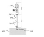
- the conventional reference electrode has a structure in which a conductive wire 2A1 is embedded in a glass tube 2A2 filled with a saturated liquid 2A3.
- KCl, NaCl solution or the like is used as the saturated liquid 2A3
- Ag / AgCl line or the like is used as the conductive wire 2A1.
- the glass tube is filled with a saturated solution with a high concentration until saturation, so that even if the solution 1A2 diffuses into the glass tube, it does not affect the conductive wires. Make electrical connections.
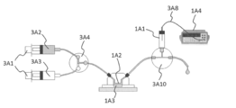
- FIG. 3 is a diagram showing an electrochemical measurement method using a conventional flow system.
- 3A1 is a syringe
- 3A2 is a sample solution
- 3A3 is a buffer solution
- 3A4 flow path switching valve 1A2 is a solution on the substrate
- 1A3 is a semiconductor substrate
- 1A1 is a reference electrode
- 3A8 is a wire
- 1A4 is a voltage source
- 3A10 is a flow path joint, as shown in Fig. 3, as a method to avoid the influence of the saturated solution, the solution is continuously flowed and the reference electrode 1A1 is installed downstream so that the saturated solution does not reach the sensor.
- a flow system is used. This configuration has the following problems and is an obstacle to the operability and miniaturization of the apparatus.
- the conventional reference electrode shown in FIG. 2 is always filled with a saturated solution in a glass tube.
- a reference electrode When measurement is not performed, it is necessary to remove the device from the apparatus and store it in a saturated solution.
- a reference electrode must be attached to the device.
- bubbles 4A1 are mixed at the tip of the reference electrode as shown in FIG. 4, the electrical connection with the solution is lost, so it is necessary to carefully remove the bubbles. These significantly impair the operability.
- the conventional reference electrode is made of a glass tube, it is difficult to reduce the size.
- the potential of the reference electrode determines the standard potential of the solution, and if noise enters here, it directly affects the detection signal. In order to avoid this, if the electromagnetic shielding is performed including the reference electrode, there is a problem that the entire apparatus becomes large.
- the present invention has been made in order to solve the above-described problems, and its purpose is to enable miniaturization, high operability, and resistance to contamination of conductive wires (that is, resistance to noise and the like). ) To realize a substance detection device and a reference electrode holding member constituting the substance detection device.
- a reference electrode holding member used in a substance detection device that electrochemically detects a substance in a solution using a reference electrode that defines an electrical standard of the solution includes at least a base material, a reference electrode holding hole formed in the base material, a reference electrode channel, and a first channel, On the base material, a sensor facing surface facing the electrochemical sensor of the substance detection device is formed, The reference electrode holding hole is formed in a portion other than the sensor facing surface of the base material, and can insert and hold a reference electrode.
- One end of the reference electrode channel forms an opening at a portion other than the sensor-facing surface of the base material, and the other end is located inside the base material.
- the tip of the reference electrode holding hole communicates with the reference electrode channel at a place other than the end of the reference electrode channel,
- One end of the first flow path forms an opening at a portion other than the sensor facing surface of the substrate, and the other end forms an opening at the sensor facing surface of the substrate.
- the other end of the reference electrode channel and the first channel communicate with each other in the base material. Reference electrode holding member.
- the reference electrode holding member according to (1) further including: (3)
- the first channel includes at least one or more branch channels, The end of the branch flow path branched from the first flow path forms an opening at the sensor facing surface, The reference electrode holding member according to the above (1) or (2).
- Two or more first flow paths are provided, In each of the first flow paths, one end forms an opening at a portion other than the sensor facing surface of the base material, the other end forms an opening at the sensor facing surface of the base material, and each of the first flow paths At least one of the one flow paths communicates with the reference electrode flow path within the base material.
- the reference electrode is a conductor wire, and when inserted and held in the reference electrode holding hole, at least a part of the conductor wire is located in the reference electrode flow path,
- the reference electrode holding member according to (6) an electrochemical sensor for electrochemically detecting a substance in the solution, and a voltage source,
- a substance detection device comprising at least (8) A valve for switching the solution supplied to the reference electrode channel and the first channel,
- the substance detection apparatus according to (7) above comprising: (9)
- the electrochemical sensor can detect at least one of potential, current, and impedance.
- the reference electrode holding member of the present invention When a substance detection device is manufactured using the reference electrode holding member of the present invention, the reference electrode is always placed in the same environment and can provide an invariable reference potential.
- the reference electrode holding member of the present invention has a configuration in which the reference electrode holding member is set to face the sensor by devising the arrangement of the reference electrode holding hole, the reference electrode channel, and the first channel. Can be cleaned. By adopting these configurations, the glass tube and the saturated solution can be eliminated from the reference electrode, the reference electrode becomes compact, and the substance detection apparatus can be downsized.
- the figure which shows the principle of the conventional reference electrode The figure which shows the reference electrode used conventionally.
- (A) And (B) is a conceptual diagram in case this invention has one 1st flow path.
- (A) is a conceptual diagram in case this invention has two or more 1st flow paths.
- (B) is a conceptual diagram in case the 1st flow path has a some branch flow path in this invention.
- (C) is a conceptual diagram when there are a plurality of second flow paths in the present invention.
- (D) is a conceptual diagram when the 2nd channel has a plurality of branch channels in the present invention.
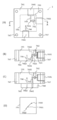
- FIG. 1 It is a figure which shows the Example of this invention, (A) is a top view, (B) and (C) are sectional drawings, (D) is a bottom view. The figure which shows the fixing method of the reference electrode in this invention. (A) And (B) is a figure which shows the control method of the solution of this invention. (A)-(C) are figures which show the flow of the solution of this invention.
- (A) is a photograph substituted for a drawing, and is a photograph of the produced substance detection apparatus.
- (B) is a drawing substitute photograph, which is a photograph of the produced reference electrode holding member.
- (C) is a photograph substituted for a drawing and a photograph of the produced reference electrode.
- FIG. 1 It is a figure which shows the mounting method of the printed circuit board used by this invention
- A) is a top view
- B) is sectional drawing.
- C) is a drawing substitute photograph, a photograph of the produced printed circuit board
- D is a drawing substitute photograph, an enlarged photograph of the semiconductor substrate portion.
- A) And (B) is a figure substitute photograph and is a figure which shows the handling method of the printed circuit board used by this invention.
- A) And (B) is a photograph substituted for a drawing, showing a connection between a holding cover of a reference electrode holding member and a semiconductor substrate.
- (A) And (B) is the figure which showed the method of incorporating a microchannel on a semiconductor substrate.
- A is the figure which showed one example of the detection of the biological substance using the substance detection apparatus of this invention.
- B is a drawing-substituting photograph and a micrograph of the electrode part.
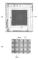
- A) is a photograph substituted for a drawing, showing a sensor array provided on the first semiconductor substrate.
- (B) is a drawing substitute photograph, and an enlarged photograph of the sensor array.
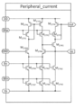
- the mixer circuit diagram used with the array peripheral circuit of the 2nd semiconductor substrate.
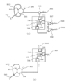
- FIG. 5A is a configuration diagram when there is one first flow path, the first flow path is used as a sample flow path, and the second flow path is used as a waste liquid flow path.
- 5A1 is the sample flow path (first flow path)
- 5A2 is the reference electrode flow path
- 5A3 is the waste liquid flow path (second flow path)
- 5A4 is the reference electrode of the present invention
- 1A3 is the semiconductor substrate
- 5A6 is the electrochemical sensor ( A semiconductor integrated circuit sensor (hereinafter sometimes simply referred to as “sensor”). Since the buffer solution constantly flows from the reference electrode channel 5A2 toward the semiconductor substrate 1A3, the sample flowing through the sample channel 5A1 does not reach the reference electrode 5A4.
- the reference electrode cleaning liquid when cleaning the reference electrode 5A4, the reference electrode cleaning liquid may be flowed from the sample channel 5A1 (first channel). Since the reference electrode cleaning liquid that has flowed through the sample flow path 5A1 (first flow path) flows to the reference electrode flow path 5A2 that communicates with the sample flow path 5A1 (first flow path), the reference electrode 5A4 can be cleaned. it can. At this time, the reference electrode channel 5A2 may be sucked in order to facilitate the flow of the reference electrode cleaning liquid into the reference electrode channel 5A2. Note that the sensor may be damaged when the reference electrode cleaning liquid flows into the sensor.
- the reference electrode cleaning liquid when flowing the reference electrode cleaning liquid, the reference electrode cleaning liquid may not flow to the sensor by flowing the buffer liquid from the waste liquid flow path 5A3 (second flow path) toward the sensor 5A6.
- the reference electrode cleaning liquid is allowed to flow from the sample channel 5A1 (first channel).
- the sample channel 5A1 ( The first flow path) and the cleaning flow path for flowing the reference electrode cleaning liquid may be separated. Since the sample liquid flows through the sample channel 5A1 (first channel) and is supplied to the sensor 5A6 on the semiconductor substrate 1A3, an appropriate potential relationship between the semiconductor substrate 1A3 and the solution is established. Can do.
- FIG. 5B is a configuration diagram when there is one first flow path, the first flow path is used as the waste liquid flow path 5A3, and the second flow path is used as the sample flow path 5A1.
- the sample liquid supplied to the sensor from the sample flow path 5A1 (second flow path) is discharged from the waste liquid flow path 5A3 (first flow path).
- the buffer solution constantly flows through the reference electrode channel 5A2, but the reference electrode channel 5A2 communicates in the middle of the waste solution channel 5A3 (first channel). Therefore, since the buffer solution flows together with the sample solution to the waste fluid channel 5A3 (first channel), the sample flowing through the waste fluid channel 5A3 (first channel) does not reach the reference electrode 5A4.
- the reference electrode cleaning solution may be flowed into the reference electrode channel 5A2 instead of the buffer solution.
- the sample liquid flows through the sample flow path 5A1 (second flow path) and is supplied to the sensor 5A6 on the semiconductor substrate 1A3, and flows through the waste liquid flow path 5A3 (first flow path), it is discarded. A proper potential relationship between 1A3 and the solution can be established.
- FIG. 6A is a diagram showing a configuration when there are a plurality of first flow paths (sample flow paths) and sensors.
- three sample flow paths 5A1 first flow paths
- the reference electrode channel 5A2 communicates with at least one of the sample channels 5A1 (first channel) in the middle of the channel. Since the sample solution flowing through each sample channel 5A1 (first channel) is supplied to the sensor 5A6, the reference electrode 5A4 is electrically connected to all the sample channels 5A1 via the solution on the semiconductor substrate 1A3. It can be performed.
- FIG. 6A is a diagram showing a configuration when there are a plurality of first flow paths (sample flow paths) and sensors.
- three sample flow paths 5A1 first flow paths
- the reference electrode channel 5A2 communicates with at least one of the sample channels 5A1 (first channel) in the middle of the channel. Since the sample solution flowing through each sample channel 5A1 (first channel) is supplied to the sensor 5A6, the reference electrode 5A4 is electrically connected to all the sample channels
- the reference electrode channel 5A2 communicates with one sample channel 5A1 (first channel), but all of the reference electrode holding member base materials are used.
- the sample channel 5A1 (first channel) may be communicated. Since the buffer solution flows from the reference electrode channel 5A2 toward the semiconductor substrate 1A3, the sample flowing through the sample channel 5A1 does not reach the reference electrode 5A4.
- the plurality of first flow paths 5A1 serve as a flow path for supplying the sample liquid containing the substance to be detected to the plurality of sensors 5A6 in the solution.
- the waste liquid flow path 5A3 (second flow path) functions as a flow path for discharging the sample liquid and the buffer liquid supplied to the sensor 5A6.
- the waste liquid channel 5A3 (second channel) includes the branch channel 5A31 having an end near each sensor 5A6, but there is no branch channel 5A31. Also good.
- the number of sample flow paths 5A1 (first flow paths) is not particularly limited, but as will be described later, the sample flow paths 5A1 (first flow paths) are formed so as to pass through the base material of the reference electrode holding member. Therefore, the number of the base material and the thickness of the sample channel 5A1 (first channel) may be taken into consideration so that the strength of the base material can be maintained.
- FIG. 6B is a diagram showing a configuration when the sample channel (first channel) includes a branch channel.
- a branch channel 5A11 is formed in the middle of one sample channel 5A1 (first channel), and the other end of each branch channel 5A11 faces the sensor 5A6. Except for this, the embodiment is the same as the embodiment shown in FIG. In the embodiment shown in FIG. 6B, the sample liquid can be supplied without being affected by the chemical reaction on the other sensor even if there is only one device such as a pump for supplying the sample liquid.
- FIG. 6C shows an embodiment in which a plurality of second flow paths (sample flow paths 5A1) and sensors 5A6 are provided in the embodiment shown in FIG. 5B, and other configurations are shown in FIG. Same as B).
- FIG. 6 (D) has the same configuration as the embodiment shown in FIG. 6 (C) except that the branch channel 5A11 is formed in the middle of one second channel (sample channel 5A1).
- the reference electrode is a conductor wire (conductive wire), but this is because replacement is easy.
- a general-purpose wire such as gold or platinum can be used as the conductor wire (conductive wire) as the reference electrode.
- FIGS. 7A and 7B are diagrams for explaining the outline of the reference electrode holding member of the present invention.
- FIG. 7A is a plan view
- FIGS. 7B and 7C are cross-sectional views taken along line AA in FIG.
- FIG. 7D is a bottom view.
- the reference electrode holding member 1 includes a base 7A1, a reference electrode holding hole 7A2 formed in the base 7A1, a reference electrode flow path 7A3, and a first flow path 7A4. At least.
- the base material 7A1 is not particularly limited as long as it is a material that does not react with a sample or the like, and examples thereof include polycarbonate, quartz, and Teflon (registered trademark).
- a sensor facing surface 7A5 facing the sensor 5A6 is formed on the base material 7A1.
- the reference electrode holding hole 7A2 may be formed anywhere as long as it is a part other than the sensor facing surface 7A5 of the base material 7A1.
- One end of the reference electrode channel 7A3 forms an opening 7A31 at a portion other than the sensor facing surface 7A5 of the base material 7A1. As shown in FIGS. 7A to 7C, the opening 7A31 may be larger than the channel width of the reference electrode channel 7A3 in order to facilitate connection to a tube or the like.
- the other end 7A32 of the reference electrode channel 7A3 is located inside the base material 7A1.
- the tip 7A21 of the reference electrode holding hole 7A2 communicates with the reference electrode channel 7A3 at a place other than the end portions 7A31 and 7A32 of the reference electrode channel 7A3. Therefore, when a reference electrode of the present invention, which will be described later, is inserted and held in the reference electrode holding hole 7A2, at least a part of the conductor wire that is the reference electrode can be positioned in the reference electrode channel 7A3.
- one end forms an opening 7A41 at a portion other than the sensor facing surface 7A5 of the substrate 7A1, and the other end forms an opening 7A42 at the sensor facing surface 7A5 of the substrate 7A1.
- the opening 7A41 may be larger than the channel width of the first channel 7A4 in order to facilitate connection to a tube or the like.
- the other end 7A32 of the reference electrode channel 7A3 and the first channel 7A4 communicate with each other in the base material 7A1.
- the reference electrode holding member 1 may include a second flow path 7A6 as necessary.
- One end of the second flow path 7A6 forms an opening 7A61 at a portion other than the sensor facing surface 7A5 of the base 7A1, and the other end forms an opening 7A62 at the sensor facing surface 7A5 of the base 7A1.
- the opening 7A61 may be larger than the channel width of the second channel 7A6 in order to facilitate connection to a tube or the like.
- the sample liquid may be supplied to the sensor 5A6 and the waste liquid on the sensor 5A6 may be sucked using a tube or the like.
- an attachment hole 7A7 for attaching to the substance detection device with a screw or the like may be formed as necessary.
- the reference electrode holding hole 7A2, the reference electrode flow path 7A3, the first flow path 7A4, the second flow path 7A6, the openings 7A31, 7A41, 7A61, and the attachment hole 7A7 may be formed by drilling the base material 7A1.
- FIG. 7C is a cross-sectional view showing another embodiment of the reference electrode holding member 1 of the present invention.
- the sheet portion 7A8 is formed on the base material 7A1, and the sensor facing surface 7A5 is formed on the sheet portion 7A8.
- the function of the seat portion 7A8 will be described later.
- the opening 7A42 of the first flow path 7A4 and the opening 7A62 of the second flow path 7A6 may be formed on the sensor facing surface 7A5 of the sheet portion 7A8.
- FIG. 7D is a bottom view showing another embodiment of the reference electrode holding member 1 of the present invention.
- the third flow path 7A51 is formed in the sensor facing surface 7A5.
- the number and shape of the third flow path 7A51 are not particularly limited, and may be appropriately adjusted according to the number and arrangement of the sensors 5A6.
- the third flow path 7A51 may be formed by cutting with a drill or the like. Further, when the base material 7A1 or the sheet portion 7A8 is a flexible material such as PDMS, a mold having a convex portion corresponding to the third flow path 7A51 may be produced and transferred.
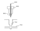
- FIG. 8 is a diagram showing a method of fixing the reference electrode in the present invention.
- 8A1 is a reference electrode fixing screw
- 5A4 is a reference electrode (conductor wire)
- 8A3 is an O-ring
- 7A2 is a reference electrode holding hole.
- a hole is made in the center of the screw
- a reference electrode 5A4 (conductor wire) is passed through, and fixed to the reference electrode holding hole 7A2 through an O-ring 8A3 for preventing water leakage. Since the tip of the reference electrode holding hole 7A2 and the reference electrode channel 7A3 communicate with each other, the tip of the reference electrode 5A4 (conductor wire) can be located in the reference electrode channel 7A3. Therefore, since the reference electrode 5A4 contacts the buffer solution flowing in the reference electrode channel 7A3, it is not contaminated by the sample solution or the like.
- FIG. 9A is a diagram showing a solution flow control method when the first flow path 7A4 is used as the sample flow path and the second flow path 7A6 is used as the waste liquid flow path.
- 3A2 is the sample solution
- 3A3 is the buffer solution
- 9A3 is the waste solution
- 9A4 is the valve (6-way valve)
- 9A5, 9A7, 9A8 is the valve (3-way valve)
- 9A6 is the reference electrode cleaning solution
- 9A9 is the buffer solution
- 9A10 is a waste liquid
- 5A4 is a reference electrode
- 1A3 is a semiconductor substrate
- 9A13 is a tube for measuring a sample liquid. The amount of change due to the sample is detected by storing the sample in a tube 9A13 having a predetermined volume and supplying the sample to the semiconductor substrate 1A3 continuously with the buffer solution not containing the sample.
- FIG. 9B is a diagram showing a control method of the solution flow when the first flow path 7A4 is used as the waste liquid flow path and the second flow path 7A6 is used as the sample flow path.
- the second flow path 7A6 only needs to be able to supply the sample liquid.
- the first flow path only needs to be able to suck and waste the waste liquid on the semiconductor substrate 1A3 and the buffer liquid 9A9 flowing in the reference electrode flow path 7A3.
- a reference electrode cleaning solution may be flowed instead of the buffer solution 9A9.
- the switching of the flow path can be simplified, the number of three-way valves can be reduced. Therefore, the substance detection device can be reduced in size.
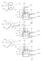
- FIG. 10 is a diagram for more specifically explaining the flow of the solution of the embodiment shown in FIG. 9 (A). (In addition, what is shown by the code
- the tube 9A13 is filled with a solution containing a sample, and the reference electrode 5A4 is cleaned with the reference electrode cleaning solution 9A6. Since the buffer liquid 9A9 flows through the second flow path 7A6 in the semiconductor substrate 1A3, the reference electrode cleaning liquid 9A6 does not reach the semiconductor substrate 1A3.
- the 6-way valve 9A4 and the 3-way valve 9A5 are switched, and the sample solution 3A2 stored in the tube 9A13 is conveyed toward the semiconductor substrate 1A3 through the first flow path 7A4. .
- the reference electrode cleaning liquid 9A6 after the three-way valve 9A5 is pushed out by the buffer liquid 3A3.
- the three-way valves 9A7 and 9A8 are switched so that the buffer solution 9A9 flows into the reference electrode 5A4 and the sample solution 3A2 does not reach the reference electrode 5A4.
- the buffer solution 9A9 only needs to prevent the sample solution 3A2 from reaching the reference electrode 5A4, and sending it very slowly reduces the effect on the composition of the solution containing the sample.
- FIG. 11 (A) is a photograph of the entire substance detection device produced, and it is compact including the reference electrode 5A4.
- power source noise is reduced by using battery driving as a voltage source.
- Electromagnetic noise can be further reduced by covering the reference electrode holding member 1 including the reference electrode 5A4 with a metal lid.
- FIG. 11B is a photograph of the reference electrode holding member 1 produced by cutting polycarbonate using a drill.
- the reference electrode holding member 1 shown in FIG. 11 (B) has one first flow path 7A4 and one second flow path 7A6, and the openings other than the sensor facing surface 7A5 of each flow path are formed wide. It is connected to the tube using 1 / 4-28UNF (unified fine thread) screws.
- FIG. 11C is a photograph of the reference electrode 5A4.
- 8A1 is a reference electrode fixing screw
- 5A4 is a reference electrode (gold wire)
- 8A3 is an O-ring
- 11B is an enlarged photograph of a part of the substance detection apparatus shown in FIG. 11A
- the reference electrode holding member 1 shown in FIG. 11B is the reference electrode holding shown in FIG. Corresponds to member 1.
- a reference electrode 5A4 illustrated in FIG. 11C corresponds to the reference electrode 5A4 illustrated in FIG.
- the semiconductor substrate 1A3 that comes into contact with the sample solution is placed on the printed circuit board shown in FIG. 12A, 12B, and 12D
- 12A1 is a printed circuit board
- 1A3 is a semiconductor substrate
- 12A3 is a bonding wire
- 12A4 and 12A5 are silicon sheet frames (frame bodies)
- 12A6 is silicon paste
- 12A7 is Counter electrode for water leakage detection
- 12A8 is a hole (extraction part) for taking out the printed circuit board
- 12A9 is the opening 7A42 of the first flow path 7A4 of the reference electrode holding member 1 and the opening 7A62 of the second flow path 7A6
- the solution entry / exit position facing the surface.
- the printed circuit board 12A1 is provided with a counter electrode 12A7 for detecting the leakage of the solution. When the solution leaks, the electrical resistance between the counter electrodes decreases, and an externally connected LED emits a warning.
- 12C is a photograph of the printed circuit board
- FIG. 12D is an enlarged photograph of the portion of the semiconductor substrate 1A3. The position of the solution inlet / outlet position 12A9 of the semiconductor substrate 1A3, the silicon sheet frame 12A4, and the reference electrode holding member 1 is shown. Indicates the positional relationship.
- the printed circuit board 12A1 is connected to the edge connector, but this connection is hard, and it takes a certain amount of force to remove the printed circuit board 12A1. Since the printed circuit board 12A1 is fixed in the apparatus, an opening (hole) 12A8 is provided in a part of the printed circuit board for removal, and tweezers 13A1 (extraction tool) shown in FIG. 13 is used. In this case, the extraction protrusion of the tweezers 13A1 is fitted into and removed from the opening (hole) 12A8 of the printed circuit board.
- FIG. 14 is a view showing an example of the substance detection device 1-1 of the present invention, and is a side view showing the connection between the reference electrode holding member 1 and the printed circuit board 12A1.
- 12A1 is a printed circuit board
- 14A1 is a printed circuit board holding part for holding the printed circuit board 12A1
- 1A3 is a semiconductor substrate
- 14A3 is a magnet
- 12A4 is a silicon sheet frame (frame body)
- 7A8 is a sheet part.
- the reference electrode holding member 1 is a reference electrode holding member
- 14A7 is a holding cover (supporting member) for the reference electrode holding member 1
- 14A8 is an alignment pin for the reference electrode holding member 1
- 14A9 is a spring (elastic member)
- 14A10 is a silicon sheet for contact ( Sheet material)
- 14A11 is a fixed stainless steel plate of the reference electrode holding member 1
- 14A2 is a pin insertion hole for inserting the alignment pin 14A8.
- the reference electrode holding member 1 and the semiconductor substrate 1A3 are mounted so as to face each other via the fixed stainless steel plate 14A11. However, the reference electrode holding member 1 is directly opposed to the semiconductor substrate 1A3. It may be attached.
- the reference electrode holding member 1 is fixed to a stainless steel plate 14A11, and a positioning pin 14A8 and a spring 14A9 are provided on the stainless steel plate.
- a sheet portion (made of silicon sheet) 7A8 is formed on the lower surface of the reference electrode holding member 1. Therefore, water leakage is prevented by being in close contact with the silicon sheet 12A4 on the semiconductor substrate 1A3 fixed to the printed circuit board 12A1.
- the lid 14A7 holds the stainless steel plate through the silicon sheet 14A10.
- FIG. 15 is a photograph showing the connection between the holding lid 14A7 of the reference electrode holding member 1 and the semiconductor substrate.
- FIG. 16 shows a configuration diagram when a flow path using PDMS (polydimethylsiloxane, hereinafter simply referred to as “PDMS”) is formed on the semiconductor substrate 1A3.
- PDMS polydimethylsiloxane
- 12A4 is a silicon sheet frame
- 1A3 is a semiconductor substrate
- 16A3 is a PDMS holding base
- 16A4 is PDMS.
- FIG. 16B is a schematic cross-sectional view when a flow path is formed. As shown in the schematic cross-sectional view of FIG.
- the PDMS cage 16A4 provided with the flow path is fixed to a PDMS holding base 16A3 serving as a PDMS support base and is in close contact with the surface of the semiconductor substrate 1A3.
- a PDMS holding base 16A3 serving as a PDMS support base
- the silicon sheet frame 12A4 and the PDMS 16A4 are not in contact with each other.
- the opening 7A42 of the first flow path 7A4 and the opening 7A62 of the second flow path 7A6 of the reference electrode holding member 1 and the holes of the PDMS 16A4 face each other, the flow path formed by the semiconductor substrate 1A3 and the PDMS 16A4 Sample liquid can be introduced and discharged.
- a plurality of first or second flow paths are formed, a plurality of holes may be formed at locations corresponding to the PDMS 16A4.
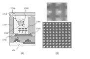
- FIG. 17 is a view showing an example of detection of a biological substance using the substance detection apparatus of the present invention
- FIG. 17 (A) is a schematic sectional view
- FIG. 17 (B) is a micrograph of an electrode portion.
- 17A1 is a molecule to be detected
- 17A2 is a bead
- 17A3 is a probe molecule
- 17A4 is a self-assembled monolayer
- 17A5 is an electrode
- 17A6 is polyimide
- 17A7 is SU-8 (a type of negative photoresist, Hereinafter, it is simply referred to as “SU-8”)
- 17A8 is PDMS
- 1A3 is a semiconductor substrate.
- An integrated circuit is formed on the semiconductor substrate 1A3, and an electrode 17A5 made of a metal such as gold, silver, or platinum, or a semiconductor such as diamond or silicon is formed on the uppermost wiring layer. It is formed.
- a metal such as gold, silver, or platinum, or a semiconductor such as diamond or silicon
- gold has a low ionization tendency and is a stable metal even in contact with a solution. Therefore, it is desirable to use gold as an electrode.
- the surface of the semiconductor substrate 1A3 is provided with a polyimide 17A6 and SU-8 micro-channel 17A7 as a protective film, and a PDMS 17A8 having a relatively large channel is in close contact therewith.
- a self-assembled monolayer 17A4 is provided on the electrode 17A5.
- a trench is formed on the sensor with SU-8 17A7, and a detection molecule 17A3 such as an enzyme, antibody, primer, etc. is fixed to a bead having a diameter of about 10 microns and placed in the trench.
- the detection target molecule 17A1 causes a chemical reaction with the probe molecule 17A3 on the bead 17A2, and the result is detected as a change in potential.
- the magnetic beads When the magnetic beads are used for the beads 17A2, they can be brought close to the surface of the semiconductor substrate 1A3 by a magnet, and the detection signal increases.
- a magnet 14A3 In the substance detection apparatus shown in FIG. 14, a magnet 14A3 can be inserted directly under the semiconductor substrate 1A3. If the bead 17A2 covers the electrode 17A5, there is a problem that the chemical reactant is not supplied to the electrode 17A5. In order to avoid this, as shown in FIG. 17B, the center of the trench is shifted from the center of the electrode 17A5.
- probe molecule 17A3 hexokinase, Glucose-6-phosphate
- three enzymes, dehydrogenase and diaphorase are immobilized on one bead 17A2 using an avidin-biotin bond, and 11-FUT is used as a self-assembled monolayer 17A4.
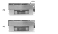
- FIG. 18A is a photograph showing the sensor array provided on the first semiconductor substrate 1A3, and FIG. 18B is an enlarged photograph of the sensor array before forming the SU-8 17A7.
- 64 ⁇ 64 sensors are arranged on the array, and at the same time, changes in potential due to 4096 types of reactions can be detected.
- 18A and 18B, 18A1 is a sensor array, and 17A5 is an electrode.
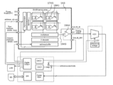
- FIG. 19 shows the configuration of the first semiconductor substrate and the external interface circuit of the substance detection apparatus of the present invention.
- 1A3 is a semiconductor substrate
- 17A5 is an electrode
- 18A1 is a sensor array 19A4, an output buffer
- 19A5 is a calibration changeover switch sensor circuit.
- the potential detection type sensor of Patent Document 1 is used for 19A3.
- the signal is output through the buffer circuit 19A4, but in order to correct an error after the buffer circuit, a voltage is applied from the outside by the switch 19A5 and the result is measured to reduce the error to 1/10 or less.
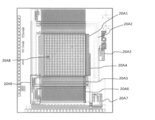
- FIG. 20 is a photograph of a second semiconductor substrate on which a sensor array for simultaneously detecting changes in potential, current, and impedance used in the substance detection apparatus of the present invention is integrated.
- 20A1 is a Y decoder
- 20A2 is a heater
- 20A3 is a thermometer
- 20A4 is a Y address buffer
- 20A5 is a current integrator
- 20A6 is an analog-digital converter and parallel input-serial output shift register
- 20A7 is a thermometer.
- 20A8 is a sensor cell
- 20A9 is a clock generation circuit.
- the sensor cells 20A8 that detect potential, current, and impedance are arranged in an array of 1024 32x32 on the substrate. Further, a Y ⁇ decoder 20A1, a Y address buffer 20A4, a current integrator 20A5, an analog-digital converter, a parallel input-serial output shift register 20A6, and a clock generation circuit 20A9 are integrated on the substrate. Further, wiring (heater) 20A2, thermometer 20A3, and thermometer preamplifier 20A7 are integrated on the substrate to control the temperature.
- the chemical reaction time is usually a few milliseconds, which is six orders of magnitude longer than the integrated circuit processing time. There is no advantage of performing the detection time at high speed, and it is effective to improve accuracy by effectively using a long time.
- the signals are averaged using the integrated signals instead of using a single signal. Since the current is a time derivative of the charge amount, the current can be integrated by storing it as a charge in the capacitor. In order to integrate the electric potential, the electric potential is temporarily replaced with a current and stored in the capacitor as electric charge.
- Fig. 21 shows the detection method of potential, current, and impedance.
- a sensor cell and an array peripheral circuit are provided.
- the sensor cell includes a voltage-current conversion circuit and a voltage fixed current detection circuit.
- the array peripheral circuit includes a mixer, a current integration circuit, and an analog-digital conversion circuit.
- ⁇ Impedance is an alternating current and is smoothed by a mixer. Subsequent integration using the capacitor acts as a low-pass filter. The potential is converted into current in the sensor cell and integrated by the array peripheral circuit. By adopting this configuration, signals of potential, current, and impedance can be processed by one array peripheral circuit.
- FIG. 22 shows the configuration of the semiconductor integrated circuit.
- the sensor circuit 22A3 uses either a voltage-current conversion circuit or a voltage fixed current detection circuit described below.
- the detection signal is output as a digital signal by analog-digital conversion.
- As the analog-digital conversion circuit a dual slope type, a current mode ⁇ - ⁇ method or the like is used.
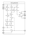
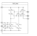
- FIG. 23 is a circuit diagram of a voltage-current conversion type sensor cell, and constant voltages Bpp and BBp are supplied by the cell bias circuit of FIG.
- two-stage source degenerate field effect transistors M23N2, M23N3, M23N4, and M23N5 are provided.
- the field effect transistor M23N7 is for operating the transistor M23N7 in the saturation region in order to fix the drain voltage of the transistor M23N1 of the sensor.
- the advantage of this circuit is that even if the input voltage VIN increases, the current flowing through the field effect transistors M23P1, M23P4, M23N6, M23N1, M23N2, and M23N4 flows through the field effect transistors M23P2, M23P5, M23N7, M23N3, and M23N5. This is not to be over. Thereby, the upper limit of the power consumption of the circuit can be set by the constant voltage Bn.
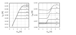
- FIG. 25 is a measurement result of current-voltage characteristics of the circuit of FIG. IBC is an output BC current, and IDD is a current flowing through the entire circuit.
- a, b, c, d, e, and f correspond to Bn voltages 2V, 1.8V, 1.6V, 1.4V, 1.2V, and 1V, respectively.
- the voltage-current converter circuit is affected by transistor threshold variations.
- a transistor M23N9 is provided in the circuit of FIG.
- FIG. 26 is a circuit diagram of a current sensor that detects a current with the potential fixed.
- FIG. 27 shows a current receiving unit at the periphery of the array that receives current signals from these sensor cells. An out potential for transferring the current is obtained with the potential of the current input portion Iin fixed.
- FIG. 28 shows a current mixer circuit.
- the product of the difference between the current flowing through M23P1 and M23P3 and the current flowing through M23P2 and M23P4 and the signal Q is output to Iout. Since the signal Q is a logic signal, the amplitude is large and the influence of the clock field through is large.
- the configuration of operational transconductance amplifiers of cascode transistors M28P1, M28P2 and folded cascode connections M28P5, M28P6, M28P7, M28P8, M28N5, M28N6, M28N7, M28N9 is adopted.
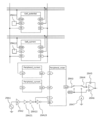
- FIG. 29 is a diagram in which these circuits are connected.
- 29A is an AC signal source (AC power supply)
- 29A2 is a phase shifter
- 29A21, 29A22, and 29A23 are inverter circuits
- 29A3 is a sample / hold switch (switch / switching means)
- 29A4 is a capacitor discharge switch (switch / switch).
- 29A7 is a capacitor discharge current source
- 29A5 is a capacitor
- 29A6 is an operational amplifier.
- the output voltage from the sensor cell is stored as a charge in the capacitor 29A5 after passing through the mixer.
- the capacitor charge is extracted by the constant current source 29A7 until the voltage of the operational amplifier 29A6 becomes the GND level.
- the switch 29A3 is for holding the output voltage of the operational amplifier.
- the operational voltage of the operational amplifier is finite, and the upper and lower limits of the output voltage of the operational amplifier are set, and when the upper or lower limit is reached, the capacitor charge is discharged and the number of times is counted. Can be increased.
- a mixer In the semiconductor integrated circuit of FIG. 20, a mixer, a current integration circuit, an analog-digital converter, and a parallel input-serial output shift register are arranged above and below the sensor array. As a result, while one is outputting the detection signal, one can accumulate the signal, and the integration time can be doubled.
- FIG. 30 is a photograph of a semiconductor integrated circuit in which an arbitrary potential is stored in an arbitrary place and applied to an electrode, and electrochemical measurement can be performed while controlling a biological material by temperature control and electrophoresis.
- the temperature can be amplified as seen in PCR. Also, temperature control is effective for increasing the accuracy of the detection signal.
- a signal change due to the temperature difference is added. In order to remove this, it is effective to make the temperature of the solution constant on the chip before the sensor.
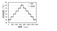
- FIG. 31 shows that the temperature can be accurately controlled as a result of controlling the temperature on the substrate using the heater and thermometer on the semiconductor substrate.
- 30A1 is a heater
- 30A2 is a thermometer
- 30A3 is an array of voltage application cells and sensor cells
- 30A4 is a voltage application electrode.
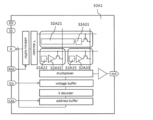
- FIG. 32 is a diagram showing a configuration of the semiconductor integrated circuit of FIG.
- the potential held in the analog memory 32A31 is applied to the electrode 32A21.
- the analog memory consists of a sample-and-hold circuit, and can hold the potential for about 10 seconds using an IpF capacitor. In order to hold the potential for a long time, it is effective to perform a refresh operation and adopt a master / slave configuration so that the potential does not change during sampling.
- the potential is stored in the voltage buffer sequentially for one column by changing the X address, and then transferred to the column specified by the Y address. Thereby, an arbitrary voltage can be applied to all the electrodes of the array.
- Electrophoresis is a standard method used in the analysis of biomolecules, but is performed by applying a voltage close to 1000 V to a distance of 10 cm. When this is done on a semiconductor substrate, the electrode distance is reduced to 100 microns and only 1V is required to achieve the same electric field.
- an electrical detection method can be used to detect a biological substance, and electrodes 32A22 and 32A23 for detecting a potential and potential detection sensor cells 32A32 and 32A33 are provided on the semiconductor integrated circuit.
- the sensor circuit can also integrate the potential, current, and impedance used in FIG.
- the substance detection apparatus that electrochemically detects a substance in the solution by the sensor 5A6 in contact with the solution, using the reference electrode 5A4 that defines the electrical standard of the solution
- the sample flow path 5A1 for supplying the sample liquid containing the substance to be detected to the sensor 5A6 in contact with the inside, and the buffer liquid for preventing the sample liquid from reaching the reference electrode 5A4 and the buffer liquid to the sensor Since the reference electrode flow path 5A2 supplied to 5A6 and the waste liquid flow path 5A3 for discharging the sample liquid and the buffer liquid that have passed through the sensor 5A6 are provided, it is possible that the sample in the solution flowing through the sample flow path reaches the reference electrode 5A4. Absent.
- the reference electrode channel 5A2 joins in the middle of the channel toward the sensor 5A6 in one sample channel 5A1 of the plurality of sample channels 5A1.
- the electrode 5A4 is easily separated from the sensor 5A6, and the reference electrode is hardly contaminated.
- the substance detection apparatus using the semiconductor integrated circuit sensor of the present invention provides a highly sensitive electrochemical measurement method with high operability and can easily detect a large amount of substances such as DNA and biomolecules. -Creates life innovation as an innovative testing and diagnostic method in the field of life sciences such as health and the environment.
- this substance detection device enables high-precision inspection by using sensor chips using high-quality semiconductor integrated circuits, and supplies a large amount of sensor chips to the bio-related industries such as medicine, pharmacy, and chemistry. By doing so, highly sensitive inspection with high operability can be easily performed, which can greatly contribute to human welfare.
- Electrochemical sensor 7A1 ... Base material, 7A2 ... Reference electrode holding hole, 7A3 ... Reference electrode channel, 7A4 ... First channel, 7A5 ... Sensor facing surface, 7A6 ... Second channel, 7A7 ... Mounting hole, 7A8 ... sheet portion, 7A21 ... tip of reference electrode holding hole, 7A31 ... opening portion, 7A32 ... other end of reference electrode flow path, 7A41 ... opening portion, 7A42 ... opening portion, 7A51 ... first Flow path, 7A61 ...
- Probe molecule 17A4 ... Self-assembled monolayer, 17A5 ... Electrode, 17A6 ... Polyimide , 17A7 ... SU-8, 17A8 ... PDMS, 18A1 ... sensor cell array, 19A4 ... output buffer, 19A5 ... calibration switch, 20A1 ... Y decoder, 20A2 ... heater, 20A3 ... thermometer, 20A4 ... Y address buffer, 20A5 ... Current integrator, 20A6: Analog-to-digital converter and parallel input-serial output shift register, 20A7 ... Thermometer preamplifier, 20A8 ... Sensor cell, 20A9 ... Clock generation circuit, 22A3 ...
Landscapes
- Chemical & Material Sciences (AREA)
- Health & Medical Sciences (AREA)
- Life Sciences & Earth Sciences (AREA)
- Physics & Mathematics (AREA)
- Immunology (AREA)
- General Physics & Mathematics (AREA)
- Chemical Kinetics & Catalysis (AREA)
- Electrochemistry (AREA)
- Analytical Chemistry (AREA)
- Biochemistry (AREA)
- General Health & Medical Sciences (AREA)
- Pathology (AREA)
- Molecular Biology (AREA)
- Spectroscopy & Molecular Physics (AREA)
- Engineering & Computer Science (AREA)
- Microelectronics & Electronic Packaging (AREA)
- Investigating Or Analyzing Materials By The Use Of Electric Means (AREA)
- Apparatus Associated With Microorganisms And Enzymes (AREA)
Abstract
Description
(1)溶液の電気的基準を定める参照電極を用いて、溶液内の物質を電気化学的に検出する物質検出装置に用いる参照電極保持部材であって、
前記参照電極保持部材は、基材、並びに、該基材に形成された参照電極保持孔、参照電極流路及び第1流路を少なくとも含み、
前記基材には、前記物質検出装置の電気化学センサに面するセンサ対向面が形成され、
前記参照電極保持孔は、前記基材の前記センサ対向面以外の部分に形成され、且つ参照電極を挿入・保持することができ、
前記参照電極流路は、一端が前記基材のセンサ対向面以外の部分で開口部を形成し、他端は前記基材内部に位置し、
前記参照電極保持孔の先端は、前記参照電極流路の端部以外の箇所で前記参照電極流路と連通し、
前記第1流路は、一端が前記基材のセンサ対向面以外の部分で開口部を形成し、他端は前記基材のセンサ対向面で開口部を形成し、
前記参照電極流路の他端と前記第1流路は、前記基材内で連通する、
参照電極保持部材。
(2)一端が前記基材のセンサ対向面以外の部分で開口部を形成し、他端は前記基材のセンサ対向面で開口部を形成する第2流路、
を更に含む、上記(1)に記載の参照電極保持部材。
(3)前記第1流路は少なくとも1以上の分岐流路を含み、
前記第1流路から分岐した分岐流路の端部は、前記センサ対向面で開口部を形成する、
上記(1)又は(2)に記載の参照電極保持部材。
(4)前記第1流路が2以上設けられ、
各々の前記第1流路は、一端が前記基材のセンサ対向面以外の部分で開口部を形成し、他端は前記基材のセンサ対向面で開口部を形成し、且つ、各々の第1流路の内、少なくとも一本は、前記参照電極流路と前記基材内で連通する、
上記(1)又は(2)に記載の参照電極保持部材。
(5)前記センサ対向面に流路が形成されている、
上記(1)~(4)の何れか一に記載の参照電極保持部材。
(6)参照電極を更に含み、
前記参照電極は導体線であり、前記参照電極保持孔に挿入・保持した時に、前記導体線の少なくとも一部が、前記参照電極流路内に位置する、
上記(1)~(5)の何れか一に記載の参照電極保持部材。
(7)上記(6)に記載の参照電極保持部材、溶液内の物質を電気化学的に検出する電気化学センサ、及び電圧源、
を少なくとも含む物質検出装置。
(8)参照電極流路及び第1流路に供給する溶液を切り替えるバルブ、
を含む、上記(7)に記載の物質検出装置。
(9)前記電気化学センサが、電位、電流、インピーダンスの少なくとも1以上を検出できる、
上記(7)又は(8)に記載の物質検出装置。
dehydrogenase、Diaphoraseの3酵素が1つのビーズ17A2にアビジン―ビオチン結合を用いて固定され、自己組織化単分子膜17A4として11-FUTを用いている。
Claims (9)
- 溶液の電気的基準を定める参照電極を用いて、溶液内の物質を電気化学的に検出する物質検出装置に用いる参照電極保持部材であって、
前記参照電極保持部材は、基材、並びに、該基材に形成された参照電極保持孔、参照電極流路及び第1流路を少なくとも含み、
前記基材には、前記物質検出装置の電気化学センサに面するセンサ対向面が形成され、
前記参照電極保持孔は、前記基材の前記センサ対向面以外の部分に形成され、且つ参照電極を挿入・保持することができ、
前記参照電極流路は、一端が前記基材のセンサ対向面以外の部分で開口部を形成し、他端は前記基材内部に位置し、
前記参照電極保持孔の先端は、前記参照電極流路の端部以外の箇所で前記参照電極流路と連通し、
前記第1流路は、一端が前記基材のセンサ対向面以外の部分で開口部を形成し、他端は前記基材のセンサ対向面で開口部を形成し、
前記参照電極流路の他端と前記第1流路は、前記基材内で連通する、
参照電極保持部材。 - 一端が前記基材のセンサ対向面以外の部分で開口部を形成し、他端は前記基材のセンサ対向面で開口部を形成する第2流路、
を更に含む、請求項1に記載の参照電極保持部材。 - 前記第1流路は少なくとも1以上の分岐流路を含み、
前記第1流路から分岐した分岐流路の端部は、前記センサ対向面で開口部を形成する、
請求項1又は2に記載の参照電極保持部材。 - 前記第1流路が2以上設けられ、
各々の前記第1流路は、一端が前記基材のセンサ対向面以外の部分で開口部を形成し、他端は前記基材のセンサ対向面で開口部を形成し、且つ、各々の第1流路の内、少なくとも一本は、前記参照電極流路と前記基材内で連通する、
請求項1又は2に記載の参照電極保持部材。 - 前記センサ対向面に流路が形成されている、
請求項1~4の何れか一項に記載の参照電極保持部材。 - 参照電極を更に含み、
前記参照電極は導体線であり、前記参照電極保持孔に挿入・保持した時に、前記導体線の少なくとも一部が、前記参照電極流路内に位置する、
請求項1~5の何れか一項に記載の参照電極保持部材。 - 請求項6に記載の参照電極保持部材、溶液内の物質を電気化学的に検出する電気化学センサ、及び電圧源、
を少なくとも含む物質検出装置。 - 参照電極流路及び第1流路に供給する溶液を切り替えるバルブ、
を含む、請求項7に記載の物質検出装置。 - 前記電気化学センサが、電位、電流、インピーダンスの少なくとも1以上を検出できる、
請求項7又は8に記載の物質検出装置。
Priority Applications (2)
| Application Number | Priority Date | Filing Date | Title |
|---|---|---|---|
| US15/556,576 US20180180566A1 (en) | 2015-03-07 | 2016-03-04 | Reference electrode holding member and substance detection device |
| JP2017505309A JP6539918B2 (ja) | 2015-03-07 | 2016-03-04 | 参照電極保持部材及び物質検出装置 |
Applications Claiming Priority (2)
| Application Number | Priority Date | Filing Date | Title |
|---|---|---|---|
| JP2015045373 | 2015-03-07 | ||
| JP2015-045373 | 2015-03-07 |
Publications (1)
| Publication Number | Publication Date |
|---|---|
| WO2016143705A1 true WO2016143705A1 (ja) | 2016-09-15 |
Family
ID=56880026
Family Applications (2)
| Application Number | Title | Priority Date | Filing Date |
|---|---|---|---|
| PCT/JP2016/056849 Ceased WO2016143705A1 (ja) | 2015-03-07 | 2016-03-04 | 参照電極保持部材及び物質検出装置 |
| PCT/JP2016/001212 Ceased WO2016143320A1 (ja) | 2015-03-07 | 2016-03-04 | 半導体集積回路 |
Family Applications After (1)
| Application Number | Title | Priority Date | Filing Date |
|---|---|---|---|
| PCT/JP2016/001212 Ceased WO2016143320A1 (ja) | 2015-03-07 | 2016-03-04 | 半導体集積回路 |
Country Status (3)
| Country | Link |
|---|---|
| US (1) | US20180180566A1 (ja) |
| JP (1) | JP6539918B2 (ja) |
| WO (2) | WO2016143705A1 (ja) |
Cited By (1)
| Publication number | Priority date | Publication date | Assignee | Title |
|---|---|---|---|---|
| JP2020535413A (ja) * | 2017-09-28 | 2020-12-03 | インターナショナル・ビジネス・マシーンズ・コーポレーションInternational Business Machines Corporation | 側方に挿入可能な電極を有するマイクロ流体デバイス |
Families Citing this family (4)
| Publication number | Priority date | Publication date | Assignee | Title |
|---|---|---|---|---|
| ES2854000T3 (es) * | 2016-11-07 | 2021-09-20 | Dnae Diagnostics Ltd | Matriz ISFET |
| WO2019099855A1 (en) * | 2017-11-17 | 2019-05-23 | Siemens Healthcare Diagnostics Inc. | Sensor assembly and method of using same |
| US20200138512A1 (en) * | 2018-11-06 | 2020-05-07 | Biosense Webster (Israel) Ltd. | Attaining Higher Impedances for Large Indifferent Electrodes |
| JP7573620B2 (ja) * | 2020-01-13 | 2024-10-25 | ベックマン コールター, インコーポレイテッド | 固体イオン選択電極 |
Citations (5)
| Publication number | Priority date | Publication date | Assignee | Title |
|---|---|---|---|---|
| JPH06148124A (ja) * | 1992-11-12 | 1994-05-27 | Hitachi Ltd | ディスポーザブルイオンセンサユニット |
| JP2000081406A (ja) * | 1998-09-04 | 2000-03-21 | Nippon Telegr & Teleph Corp <Ntt> | 極微少量フローセル、及びその製造方法 |
| JP2006242900A (ja) * | 2005-03-07 | 2006-09-14 | Mitsubishi Chemicals Corp | センサユニット及び反応場セルユニット並びに分析装置 |
| JP2011099867A (ja) * | 2002-07-31 | 2011-05-19 | Toshiba Corp | 塩基配列自動解析装置 |
| JP2012528329A (ja) * | 2009-05-29 | 2012-11-12 | ライフ テクノロジーズ コーポレーション | 電気化学的反応を行うための装置および方法 |
Family Cites Families (11)
| Publication number | Priority date | Publication date | Assignee | Title |
|---|---|---|---|---|
| US5019238A (en) * | 1984-03-28 | 1991-05-28 | Baxter Diagnostics Inc. | Means for quantitative determination of analyte in liquids |
| US4627893A (en) * | 1984-03-28 | 1986-12-09 | Amdev, Inc. | Means and methods for quantitative determination of analyte in liquids |
| JPS61169756A (ja) * | 1985-01-23 | 1986-07-31 | Hitachi Ltd | 比較電極装置 |
| JPH1194793A (ja) * | 1997-09-22 | 1999-04-09 | Research Institute Of Innovative Technology For The Earth | 光走査型二次元濃度分布測定装置 |
| JP3879579B2 (ja) * | 2002-04-22 | 2007-02-14 | 松下電工株式会社 | 水分量センサ |
| JP2003322630A (ja) * | 2002-05-01 | 2003-11-14 | Seiko Epson Corp | バイオセンサ、バイオセンシングシステム、及びバイオセンシング方法 |
| GB2457851B (en) * | 2006-12-14 | 2011-01-05 | Ion Torrent Systems Inc | Methods and apparatus for measuring analytes using large scale fet arrays |
| US8349167B2 (en) * | 2006-12-14 | 2013-01-08 | Life Technologies Corporation | Methods and apparatus for detecting molecular interactions using FET arrays |
| JP5420204B2 (ja) * | 2008-07-18 | 2014-02-19 | 株式会社船井電機新応用技術研究所 | 携帯型の物質検出装置 |
| US9274059B2 (en) * | 2011-03-14 | 2016-03-01 | Battelle Memorial Institute | Microfluidic electrochemical device and process for chemical imaging and electrochemical analysis at the electrode-liquid interface in-situ |
| JP2013220066A (ja) * | 2012-04-17 | 2013-10-28 | Hitachi Ltd | センサチップ及びそれを用いた測定方法 |
-
2016
- 2016-03-04 US US15/556,576 patent/US20180180566A1/en not_active Abandoned
- 2016-03-04 WO PCT/JP2016/056849 patent/WO2016143705A1/ja not_active Ceased
- 2016-03-04 JP JP2017505309A patent/JP6539918B2/ja active Active
- 2016-03-04 WO PCT/JP2016/001212 patent/WO2016143320A1/ja not_active Ceased
Patent Citations (5)
| Publication number | Priority date | Publication date | Assignee | Title |
|---|---|---|---|---|
| JPH06148124A (ja) * | 1992-11-12 | 1994-05-27 | Hitachi Ltd | ディスポーザブルイオンセンサユニット |
| JP2000081406A (ja) * | 1998-09-04 | 2000-03-21 | Nippon Telegr & Teleph Corp <Ntt> | 極微少量フローセル、及びその製造方法 |
| JP2011099867A (ja) * | 2002-07-31 | 2011-05-19 | Toshiba Corp | 塩基配列自動解析装置 |
| JP2006242900A (ja) * | 2005-03-07 | 2006-09-14 | Mitsubishi Chemicals Corp | センサユニット及び反応場セルユニット並びに分析装置 |
| JP2012528329A (ja) * | 2009-05-29 | 2012-11-12 | ライフ テクノロジーズ コーポレーション | 電気化学的反応を行うための装置および方法 |
Cited By (3)
| Publication number | Priority date | Publication date | Assignee | Title |
|---|---|---|---|---|
| JP2020535413A (ja) * | 2017-09-28 | 2020-12-03 | インターナショナル・ビジネス・マシーンズ・コーポレーションInternational Business Machines Corporation | 側方に挿入可能な電極を有するマイクロ流体デバイス |
| GB2581291B (en) * | 2017-09-28 | 2022-11-23 | Ibm | Microfluidic device with laterally insertable electrodes |
| JP7196162B2 (ja) | 2017-09-28 | 2022-12-26 | インターナショナル・ビジネス・マシーンズ・コーポレーション | 側方に挿入可能な電極を有するマイクロ流体デバイス |
Also Published As
| Publication number | Publication date |
|---|---|
| JPWO2016143705A1 (ja) | 2017-12-21 |
| JP6539918B2 (ja) | 2019-07-10 |
| US20180180566A1 (en) | 2018-06-28 |
| WO2016143320A1 (ja) | 2016-09-15 |
Similar Documents
| Publication | Publication Date | Title |
|---|---|---|
| JP6539918B2 (ja) | 参照電極保持部材及び物質検出装置 | |
| Tang et al. | Toward a miniature wireless integrated multisensor microsystem for industrial and biomedical applications | |
| Joo et al. | Chemical sensors with integrated electronics | |
| Milgrew et al. | A large transistor-based sensor array chip for direct extracellular imaging | |
| JP4883812B2 (ja) | 物質検出装置 | |
| US11161115B2 (en) | PH control for analyte detection | |
| JP7336983B2 (ja) | イオンセンサ装置 | |
| US20070240986A1 (en) | Microfluidic Device with Minimized Ohmic Resistance | |
| US20100300895A1 (en) | Apparatus and methods for performing electrochemical reactions | |
| US20140332410A1 (en) | Analytical micro-devices for mental health treatment monitoring | |
| Ghafar-Zadeh et al. | CMOS capacitive sensors for lab-on-chip applications | |
| Garner et al. | A multichannel DNA SoC for rapid point-of-care gene detection | |
| KR101195612B1 (ko) | 금층을 포함하는 전계 효과 트랜지스터, 상기 전계 효과 트랜지스터를 포함하는 미세유동장치, 및 상기 전계 효과 트랜지스터 및 미세유동장치를 이용하여 티올기를 포함하는 분석물을 검출하는 방법 | |
| US20080250883A1 (en) | Sensor chip and inspection device | |
| Singh | From sensors to systems: CMOS-integrated electrochemical biosensors | |
| CN113454448B (zh) | 具有可编程传感腔的生物传感器 | |
| JP2015210233A (ja) | 超並列的生体分子検出方法および装置 | |
| CN101558295A (zh) | 电化学传感器装置及其制造方法 | |
| US8617382B2 (en) | Process and device for emulating a counter-electrode in a monolithically integrated electrochemical analysis system | |
| Kim et al. | Label-free CMOS bio sensor with on-chip noise reduction scheme for real-time quantitative monitoring of biomolecules | |
| KR100778889B1 (ko) | 전기화학적 당화단백질 검출 시스템 | |
| Nam et al. | Micropotentiometric sensors | |
| Yamaoka et al. | Potentiometric glucose detection by paper-based electrochemical sensor on CMOS chip | |
| Raj et al. | Fabrication of a configurable multi-potentiostat for LOC applications | |
| Raja et al. | High-bandwidth low-current measurement system for automated and scalable probing of tunnel junctions in liquids |
Legal Events
| Date | Code | Title | Description |
|---|---|---|---|
| 121 | Ep: the epo has been informed by wipo that ep was designated in this application |
Ref document number: 16761675 Country of ref document: EP Kind code of ref document: A1 |
|
| ENP | Entry into the national phase |
Ref document number: 2017505309 Country of ref document: JP Kind code of ref document: A |
|
| NENP | Non-entry into the national phase |
Ref country code: DE |
|
| WWE | Wipo information: entry into national phase |
Ref document number: 15556576 Country of ref document: US |
|
| 122 | Ep: pct application non-entry in european phase |
Ref document number: 16761675 Country of ref document: EP Kind code of ref document: A1 |