WO2016143320A1 - 半導体集積回路 - Google Patents
半導体集積回路 Download PDFInfo
- Publication number
- WO2016143320A1 WO2016143320A1 PCT/JP2016/001212 JP2016001212W WO2016143320A1 WO 2016143320 A1 WO2016143320 A1 WO 2016143320A1 JP 2016001212 W JP2016001212 W JP 2016001212W WO 2016143320 A1 WO2016143320 A1 WO 2016143320A1
- Authority
- WO
- WIPO (PCT)
- Prior art keywords
- sensor
- current
- circuit
- potential
- array
- Prior art date
- Legal status (The legal status is an assumption and is not a legal conclusion. Google has not performed a legal analysis and makes no representation as to the accuracy of the status listed.)
- Ceased
Links
Images








Classifications
-
- G—PHYSICS
- G01—MEASURING; TESTING
- G01N—INVESTIGATING OR ANALYSING MATERIALS BY DETERMINING THEIR CHEMICAL OR PHYSICAL PROPERTIES
- G01N27/00—Investigating or analysing materials by the use of electric, electrochemical, or magnetic means
- G01N27/26—Investigating or analysing materials by the use of electric, electrochemical, or magnetic means by investigating electrochemical variables; by using electrolysis or electrophoresis
- G01N27/28—Electrolytic cell components
- G01N27/30—Electrodes, e.g. test electrodes; Half-cells
- G01N27/301—Reference electrodes
-
- G—PHYSICS
- G01—MEASURING; TESTING
- G01N—INVESTIGATING OR ANALYSING MATERIALS BY DETERMINING THEIR CHEMICAL OR PHYSICAL PROPERTIES
- G01N27/00—Investigating or analysing materials by the use of electric, electrochemical, or magnetic means
- G01N27/02—Investigating or analysing materials by the use of electric, electrochemical, or magnetic means by investigating impedance
- G01N27/028—Circuits therefor
-
- G—PHYSICS
- G01—MEASURING; TESTING
- G01N—INVESTIGATING OR ANALYSING MATERIALS BY DETERMINING THEIR CHEMICAL OR PHYSICAL PROPERTIES
- G01N27/00—Investigating or analysing materials by the use of electric, electrochemical, or magnetic means
- G01N27/02—Investigating or analysing materials by the use of electric, electrochemical, or magnetic means by investigating impedance
-
- G—PHYSICS
- G01—MEASURING; TESTING
- G01N—INVESTIGATING OR ANALYSING MATERIALS BY DETERMINING THEIR CHEMICAL OR PHYSICAL PROPERTIES
- G01N27/00—Investigating or analysing materials by the use of electric, electrochemical, or magnetic means
- G01N27/26—Investigating or analysing materials by the use of electric, electrochemical, or magnetic means by investigating electrochemical variables; by using electrolysis or electrophoresis
- G01N27/28—Electrolytic cell components
- G01N27/30—Electrodes, e.g. test electrodes; Half-cells
- G01N27/327—Biochemical electrodes, e.g. electrical or mechanical details for in vitro measurements
- G01N27/3275—Sensing specific biomolecules, e.g. nucleic acid strands, based on an electrode surface reaction
- G01N27/3276—Sensing specific biomolecules, e.g. nucleic acid strands, based on an electrode surface reaction being a hybridisation with immobilised receptors
-
- G—PHYSICS
- G01—MEASURING; TESTING
- G01N—INVESTIGATING OR ANALYSING MATERIALS BY DETERMINING THEIR CHEMICAL OR PHYSICAL PROPERTIES
- G01N27/00—Investigating or analysing materials by the use of electric, electrochemical, or magnetic means
- G01N27/26—Investigating or analysing materials by the use of electric, electrochemical, or magnetic means by investigating electrochemical variables; by using electrolysis or electrophoresis
- G01N27/403—Cells and electrode assemblies
-
- G—PHYSICS
- G01—MEASURING; TESTING
- G01N—INVESTIGATING OR ANALYSING MATERIALS BY DETERMINING THEIR CHEMICAL OR PHYSICAL PROPERTIES
- G01N27/00—Investigating or analysing materials by the use of electric, electrochemical, or magnetic means
- G01N27/26—Investigating or analysing materials by the use of electric, electrochemical, or magnetic means by investigating electrochemical variables; by using electrolysis or electrophoresis
- G01N27/403—Cells and electrode assemblies
- G01N27/414—Ion-sensitive or chemical field-effect transistors, i.e. ISFETS or CHEMFETS
Definitions
- the present invention is a substance detection device for detecting substances in a solution electrochemically by a semiconductor integrated circuit sensor and measuring the physical properties of a substance (hereinafter, including the case of detecting physical properties).
- the present invention relates to a semiconductor integrated circuit.
- a semiconductor integrated circuit for electrochemically detecting a DNA molecule, a protein, a cell, a bacterium, a virus, a biomolecule such as glucose, a biological substance, etc. as a change in potential, current, and impedance. .
- a specific biomolecule, a biological substance, or the like, or a substance detection device that detects their physical properties is detected by reacting with a detection molecule.
- a detection molecule binds only to a specific molecule or causes a chemical reaction only with a specific molecule.
- it is effective to interpose an antibody or an enzyme in order to improve detection accuracy.
- an electrochemical measurement method that detects a change in potential, current, and impedance is often used (Patent Documents 1, 4, etc.). According to Patent Document 2 below, when a substance is detected with an electric current, it takes time to stabilize to a steady value.
- a fixed voltage is applied to a cell that is not measured and the measurement cell is fixed.
- the steady current of each cell is sequentially scanned and detected at high speed.
- a detected voltage value is converted into a current pulse, and a substance is detected based on the pulse width.
- Non-Patent Document 1 describes a method of detecting the presence / absence of a molecular bond using a gate of a field effect transistor as a change in charge amount.
- Non-Patent Document 2 describes a method in which the concentration of a specific molecule is transferred to the concentration ratio of an oxidant and a reductant using an enzyme reaction, and the redox potential is detected using the gate of a field effect transistor. ing.
- Non-Patent Document 3 below describes a method of detecting the concentration of a specific molecule as an oxidation-reduction current using an enzyme reaction.
- Non-Patent Document 4 describes a method in which a specific virus is captured by an antibody provided on an electrode and detected as a change in impedance.
- Hb blood cell hemoglobin
- HbA1c hemoglobin A1c
- the photomask cost of a semiconductor integrated circuit exceeds 100 million yen per set when lithography of 100 nm or less is used. If circuits are individually designed for various applications, the unit price of the chip becomes too high, and its spread is limited.
- a semiconductor integrated circuit of a substance detection device standardization and generalization by integrating potential, current, and impedance sensors are required.
- a chip in which a sensor array for potential detection and its peripheral circuit are integrated, a chip in which a current detection sensor array and its peripheral circuit are integrated, and a sensor array for measuring impedance And its peripheral circuits are individually designed and integrated on individual chips.
- an object of the present invention is to realize a high-density integrated sensor array of potential, current and impedance by unifying signals from sensor units and unifying sensor array peripheral circuits.
- the invention for solving the above problems includes a sensor array in which sensor units that output an electric signal in response to a substance by a detection electrode are arrayed, and an array peripheral circuit that processes an electric signal output from each sensor unit.
- a sensor unit as a potential sensor that converts a potential detected by a detection electrode into a current signal and outputs the current signal to an array peripheral circuit, and the potential of the detection electrode is fixed and flows to the detection electrode.
- Three types of sensors a sensor unit as a current sensor that outputs a current signal corresponding to a current to the array peripheral circuit and a sensor unit as an impedance sensor that outputs an AC current signal detected by the detection electrode to the array peripheral circuit ( That is, at least of potential sensor, current sensor, impedance sensor)
- a semiconductor integrated circuit characterized in that a mixture of the two kinds of sensor units.
- the present invention is characterized in that the value detected by the sensor is output from the sensor as the magnitude of the current.
- a feature is that at least two types of sensors among a potential sensor, a current sensor, and an impedance sensor are mixed on one chip.
- the area on the sensor array may be divided into two or three parts, and each type of sensor unit may be arranged in each area.
- two or three of the potential sensor, current sensor, and impedance sensor may be adjacent to each other as a single set sensor, and the single set sensor may be arranged in an array to mix the sensors.
- the current sensor and the impedance sensor may have the same structure. That is, the current sensor can also be used as the impedance sensor.
- the array peripheral circuit may be a circuit that performs selective scanning of the sensor array in units of rows, inputs a current signal from the selected sensor unit, and processes the current signal.
- This array peripheral circuit is also integrated on one chip together with the sensor array.
- the sensor array includes a potential sensor and a current sensor, and the array peripheral circuit inputs a current signal output from the potential sensor and a current signal output from the current sensor, and measures a substance based on both current signals. It can be set as the circuit which does. Thereby, for example, by the simultaneous measurement of blood cells, the ratio of hemoglobin A1c in blood cell hemoglobin can be measured by the ratio of the detection potential to the detection current.
- the sensor array includes at least one of a potential sensor and a current sensor, and an impedance sensor, and the array peripheral circuit has at least one of a current signal output from the potential sensor and a current signal output from the current sensor. And a circuit for measuring a substance based on an alternating current signal output from the impedance sensor.
- the total volume of blood cells and the proportion of hemoglobin, hemoglobin A1c, glucose, etc. in the volume can be measured by simultaneous measurement of blood cells.
- a potential sensor may exist in the sensor array, and the power sensor may be provided with a power consumption control circuit that controls the maximum value of power consumption. Since the sensor array has a large number of sensors, the reaction with the detection molecules is sensitive to temperature, and heat generation of the circuit must be avoided, so that power saving is important.
- the array peripheral circuit includes a detection circuit that converts an AC signal into a DC signal, a current integration circuit that integrates the current output from the detection circuit, and an analog signal that converts the current integration signal output from the current integration circuit into a digital signal. A circuit having a digital conversion circuit can be used. AC current can be detected, and in particular, impedance can be measured.
- a potential sensor exists in the sensor array, the potential sensor includes a sensor transistor that outputs an electrical signal detected by the detection electrode, and a source degeneration transistor that defines a potential detection range is connected to the sensor transistor. It is good also as a structure. The dynamic range of potential detection can be expanded.
- the array peripheral circuit may include a circuit that controls the electric field and temperature of the solution that is in direct contact with the detection electrode or through another metal or insulating film.
- the value detected by the sensor is output as a current to a circuit that processes a signal
- noise resistance can be increased.
- the noise level can be reduced by about three orders of magnitude compared to the voltage output.
- at least two types of potential sensor, current sensor, and impedance sensor are mixed on the sensor array on one chip, various substances and physical properties can be quickly applied to the same part of the measured substance. Measurement can be performed at the same time, and the amount of information obtained is expanded.
- a high-density potential / current / impedance integrated sensor array could be realized.
- FIG. 1 is a chip photograph of a semiconductor integrated circuit according to Example 1 of the present invention.
- 1 is a diagram illustrating a circuit configuration and an interface circuit of a semiconductor integrated circuit according to a first embodiment of the present invention.
- 8 is a chip photograph of a semiconductor integrated circuit according to Example 2 of the present invention.
- the conceptual diagram which showed the method to integrate electric potential, electric current, and impedance measurement in the chip
- FIG. 5 is a diagram illustrating a configuration of a semiconductor integrated circuit according to a second embodiment of the present invention.
- FIG. 6 is a circuit diagram of a potential sensor cell constituting a semiconductor integrated circuit according to a second embodiment of the present invention.
- FIG. 6 is a bias circuit diagram of a sensor cell constituting the semiconductor integrated circuit according to the second embodiment of the present invention. The figure which shows the current-voltage characteristic of the electric potential sensor cell which comprises the semiconductor integrated circuit of Example 2 of this invention.
- the circuit diagram of the current sensor cell which comprises the semiconductor integrated circuit of Example 2 of this invention.
- FIG. 6 is a mixer circuit diagram used in an array peripheral circuit of a semiconductor integrated circuit according to a second embodiment of the present invention. The figure which connected each element circuit of the semiconductor integrated circuit of Example 2 of this invention.
- FIG. 8 is a chip photograph of a semiconductor integrated circuit according to Example 3 of the present invention. The figure which controlled temperature using the semiconductor integrated circuit of Example 3 of this invention.
- FIG. 5 is a diagram illustrating a configuration of a semiconductor integrated circuit according to a third embodiment of the present invention.
- Printed circuit board 2 Semiconductor integrated circuit chip 3 ... Silicone paste 4 ... Gold electrode 5 ... Polyimide 6 ... Micro flow path 7 ... PDMS 8 ... Self-assembled monolayer 9 ... Molecule for detection 10 ... Bead 11 ... Object to be detected Molecule 12 ... sensor array 13 ... potential detection sensor cell circuit 14 ... output buffer 15 ... calibration switch 16 ... Y decoder 17 ... heater 18 ... thermometer 19 ... Address buffer 20 ... Integration processing unit 20a ... Mixer 20b ... Current integration circuit 21a ... Analog-digital conversion circuit 21 ... Signal output unit 21b ... Parallel input-serial output shift register 22 ... Thermometer preamplifier 23 ...
- Sensor cell 23a Potential Sensor cell 23b ... Current sensor cell 23c ... Impedance sensor cell 24 ... Clock generation circuit 25 ... Potential detection sensor cell circuit 25a 25b 25c ... Sensor circuit 26 ... Capacitor 27 ... Capacitor discharge switch 28 ... Operational amplifier 29 ... Current source for capacitor discharge 30 ... Sample and hold Changeover switch 31... AC signal source 32... Phase shifter 33, 34, 35... Inverter circuit 36 ... Array for voltage application and sensor cell 37 ... Electrode for voltage application 38 ... Voltage holding circuit 39 ... Buffer 40 ... Voltage current conversion circuit 50 ... Voltage fixed current detection circuit 60 ... Array peripheral circuit 61a ... Current receiver 61b ... Reference Receiver 80 ... Si substrate 81 ...
- FIG. 1 shows an example of a substance detection device constituted by a semiconductor integrated circuit sensor.
- a semiconductor integrated circuit chip 2 mm of 7.5 mm square is die-bonded on the printed circuit board 1 and electrically connected by wire bonding, and then the wire portion is sealed with silicone paste 3 mm. Blood, saliva, collected water, etc. are flowed on the surface of the semiconductor integrated circuit chip 2, and the biological material is measured by a sensor circuit integrated on the semiconductor substrate.
- the semiconductor integrated circuit chip 2 includes thousands to tens of millions of sensor cells, and performs thousands to tens of millions of detections simultaneously. For example, the number of bases of a virus is composed of several millions, and by detecting the bases in parallel with tens of millions of sensor cells, it is possible to obtain all the gene information of the virus in 10 minutes.
- Fig. 2 shows the configuration of the sensor unit of this device, and shows an example of the detection of a biological substance using the device.
- Fig. 2 (A) is a schematic sectional view of one sensor cell, Fig. 2 (B). Is a plane micrograph of a plurality of sensor cells arranged in a two-dimensional array. An electronic circuit is formed on the semiconductor integrated circuit chip 2, and a gold electrode 4 serving as a detection electrode is formed on the uppermost wiring layer.
- 80 is a Si substrate, 81 is a source region, 82 is a drain region, and 83 is a gate, and these constitute a field effect transistor (hereinafter referred to as “FET ⁇ ”).
- FET ⁇ field effect transistor
- the substrate surface is provided with a micro flow channel 6 mm made of polyimide 5 mm and SU-8 (a kind of negative photoresist, hereinafter simply referred to as “SU-8”) as a protective film, on which a relatively large flow channel is formed.
- SU-8 a kind of negative photoresist
- a self-assembled monolayer 8 mm is provided on the gold electrode 4 mm.
- a trench 86 is formed on the sensor by a micro flow path 6 made of SU-8, and detection molecules 9 such as enzymes, antibodies, and primers are fixed to beads 10 having a diameter of about 10 microns and placed in the trench 86.
- the specimen 11 to be examined undergoes a chemical reaction with the detection molecule 9 on the bead, and the result is detected as a change in potential by the FET. If the bead 10 covers the gold electrode 4 ⁇ , there is a problem that the chemical reaction substance is not supplied to the gold electrode 4. In order to avoid this, as shown in FIGS.
- the trench 86 is arranged so that the central axis perpendicular to the opening surface of the trench 86 does not coincide with the central axis perpendicular to the surface of the gold electrode 4. And the arrangement of the gold electrode 4mm is shifted.
- Non-Patent Document 5 The results of detecting glucose in the blood by the redox potential using this configuration have been reported by the present inventors in Non-Patent Document 5 and Non-Patent Document 6.
- 9 enzymes for detection are fixed to one bead using avidin-biotin bonds, such as hexokinase, glucose-6-phosphate dehydrogenase, and diaphorase.
- 11-ferrocenyl-1- undecanthiol (11-FUT) is used as the self-assembled monolayer 8.
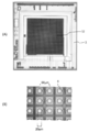
- FIG. 3 is a photograph showing the sensor array 12 provided on the second side of the semiconductor integrated circuit chip.
- FIG. 3 (B) is a micrograph of an enlarged portion of the sensor array 12 and there is a metal electrode 4 for each cell.
- 64x64 sensors are arranged in a two-dimensional array, and changes in potential due to 4096 bioreactions can be detected in parallel.
- the potential on the gold electrode 4 changes with the bioreaction, and biomolecules are detected from this change.
- the sensor cell has a size of 60 ⁇ m ⁇ 60 ⁇ m
- the opening of the gold electrode has a size of 20 ⁇ m ⁇ 20 ⁇ m.
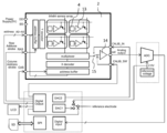
- FIG. 4 shows the configuration of two semiconductor integrated circuit chips and an external interface circuit.
- 2 is a semiconductor integrated circuit chip
- 4 is a gold electrode
- 13 is a potential sensor cell circuit (potential sensor) 14
- 14 is an output buffer
- 15 is a calibration changeover switch.
- the potential detection type sensor of Patent Document 1 and a current detection sensor or an impedance sensor are used.
- the signal is output through the buffer circuit 14, but in order to correct an error due to threshold variation after the buffer circuit, a voltage is applied from the outside through the switch 15, and the result is measured and calibrated. As a result, the error is reduced from 5mV to less than 1/10 of 0.5mV.
- FIG. 5 is a photograph of a semiconductor integrated circuit chip 2 mm in which a sensor array 12 that simultaneously detects changes in potential, current, and impedance is integrated.
- the overall configuration of the apparatus of the second embodiment is the same as that shown in FIGS.
- 16 is a Y decoder that selects one row of the sensor array 12
- 17 is a heater that changes the temperature of the semiconductor integrated circuit chip
- 18 is a thermometer that measures the temperature of the chip
- 19 is a location that selects one row of the array.
- An address buffer 20 stores an integration processor 20 comprising a mixer 20a for mixing the current signal from the sensor cell with an AC signal input from the outside, and a current integration circuit 20b for integrating the output of the mixer 20a.
- Reference numeral 21 denotes an analog-digital conversion circuit 21a for converting an analog signal output from the current integration circuit into a digital signal, and a parallel input-serial output shift register 21b for sequentially transmitting the digital signal to the outside (hereinafter referred to as "parasiri conversion circuit”).
- a signal output unit composed of, 22 is a preamplifier for amplifying the output of the thermometer 18, 23 is a sensor cell, and 24 is a clock generation circuit.
- the array peripheral circuit 60 (FIG.
- the clock generation circuit 24 is configured.
- sensor cells 23 for detecting potential, current, and impedance are arranged in a 1024 two-dimensional array of 32 ⁇ 32 cm.
- a potential sensor cell 23a which is a potential sensor
- a current sensor cell 23b which is a current sensor
- an impedance sensor cell 23c which is an impedance sensor
- the impedance sensor cell 23c detects an alternating current
- the current sensor cell 23b also serves as the impedance sensor cell 23c in this embodiment. Accordingly, one particular current sensor cell 23b detects current, and another particular current sensor cell 23b becomes an impedance sensor cell 23c, which measures impedance.
- the impedance sensor cell 23c may be provided independently as a sensor cell having a structure different from that of the current sensor cell 23b. Further, in the periphery of the sensor array 12, one Y decoder 16 per row and two upper and lower integration processing units 20 and signal output units 21 per row are integrated. Furthermore, the temperature of the substrate can be set from room temperature to 120 ° C. by the wiring (heater) 17, the thermometer 18, and the preamplifier 22 of the thermometer.
- the chemical reaction time is usually a few milliseconds, which is six orders of magnitude longer than the integrated circuit processing time. There is no advantage of performing the detection time at high speed, and it is effective to improve accuracy by effectively using a long time.
- the signals are averaged using the integrated signals rather than using a single signal. Since the current is a time derivative of the charge amount, the current can be integrated by storing it as a charge in the capacitor. In order to integrate the electric potential, the electric potential is temporarily replaced with a current and stored in the capacitor as electric charge.
- FIG. 6 is a block diagram relating to the potential, current, and impedance detection circuit of FIG.
- the potential sensor cell 23a has a voltage / current conversion circuit 40 for converting the detected potential into current
- the current sensor cell 23b and the impedance sensor cell 23c have a voltage fixed current detection circuit 50.
- the array peripheral circuit 60 includes a mixer 20a, a current integrating circuit 20b, an analog-digital converter circuit 21a, and a parallel-serial converter circuit 21b.
- the outputs of the voltage / current conversion circuit 40 and the voltage fixed current detection circuit 50 are both input to the array peripheral circuit 60 as current signals.
- the impedance detection signal output from the impedance sensor cell 23c is an alternating current and is smoothed by the mixer 20a.
- the subsequent current integrating circuit 20b serves as a low-pass filter.
- the potential is converted into a current in each sensor cell 23 and integrated by the array peripheral circuit 60.
- signals of potential, current, and impedance can be processed by one array peripheral circuit 60.
- the mixer 20a smoothes and converts an AC signal into a DC signal in impedance detection.
- the frequency of the AC signal source 31 is 0 Hz, that is, a constant voltage source.
- a low frequency signal of several Hz to several kHz can be given and used as a lock-in amplifier to reduce noise.
- Fig. 7 shows the configuration of the semiconductor integrated circuit.
- the same circuits as those described in FIGS. 5 and 6 are denoted by the same reference numerals.
- the sensor circuit 25a of the potential sensor cell 23a is a voltage-current conversion circuit (open circuit voltage sensor) described below.
- the sensor circuit 25b of the current sensor cell 23b and the sensor circuit 25c of the impedance sensor cell 23c are voltage fixed current detection circuits (closed current sensors). ).
- the detection signal is output to the outside as a serial digital signal via the analog-digital conversion circuit 21a and the parallel-serial conversion circuit 21b.
- the analog-digital conversion circuit 21a for example, a dual slope type, a current mode delta-sigma method or the like is used.
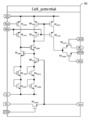
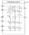
- FIG. 8 is a circuit diagram of the voltage / current conversion type potential sensor cell 23a.
- the constant voltages Bpp and BBp are supplied by the cell bias circuit of FIG.
- the maximum current flowing in the circuit of the potential sensor cell 23a in FIG. 8 is determined by the constant voltage Bn in FIG.
- the output Bp in FIG. 9 can transmit the set value by being connected to Bn of the cell bias circuit in the next stage. In the configuration in which Bn is connected to Bn in the next stage, an error occurs due to a voltage drop due to wiring. However, by transmitting the current as such, the set value can be accurately transmitted.
- two-stage source degeneration transistors (diodes) M23N2, M23N3, M23N4, and M23N5 are provided.
- the potential (Vin) of the gold electrode 4 (detection electrode) is applied to the gate of the transistor M23N1.
- This detection potential Vin is converted into a drain current flowing through the transistors M23N1, M23N2, and M23N4.
- the gate of the transistor M23N7 is connected to the source of the transistor N23N6, and the gate of the transistor N23N6 is connected to the drain of the transistor M23N7.
- the transistor M23N7 is a transistor for keeping the transistor M23N1 in the saturation region
- the transistor M23N6 is a transistor for keeping the transistor M23N7 in the saturation region.
- the current flowing through the current detection circuit consisting of the cascode connection of transistors M23P1, M23P4, M23N6, M23N1, M23N2, and 23M23N4 is the transistor M23P2, M23P5, M23N7, M23N3, M23N5 That is, the current Iss flowing through the current limiting circuit composed of the cascode connection should not be exceeded.
- the current Iss flowing in the current limiting circuit is determined by a constant voltage Bn (Bpp and BBp determined by Bn), and the gate-source voltage VGSs of the transistors M23N3 and M23N5 is determined by the current Iss.
- M23N1 enters the linear region (triode region) when the detection potential VinV exceeds 3VGSs, the current flowing through the current detection circuits of the transistors M23P1, M23P4, M23N6, M23N1, M23N2, and M23N4 does not exceed Iss.
- the upper limit of the power consumption of the circuit can be set by the constant voltage Bn.
- the bioreaction is sensitive to temperature, and if the power consumption of the semiconductor integrated circuit is large, it generates heat and raises the temperature, making it impossible to accurately identify the amount of biomolecules.
- the power consumption of a semiconductor integrated circuit capable of ignoring the temperature rise is 1 mW / cm 2 or less, and when 1000 sensor cells are integrated, it is necessary to limit the current that can be passed to one sensor cell to 1 uA or less.
- BC is connected to the input terminal of the array peripheral circuit 60 at the output terminal of the potential sensor cell 23a.
- the array peripheral circuit 60 keeps the voltage at the terminal BC at the same voltage as GND.
- Transistors M23P7 and M23N8 are complementary output circuits controlled by their respective gate voltages so that when one is on, the other is off.
- the output signal from the terminal BC is a current signal obtained by converting the detected potential into a current.
- the transistor M23P7 When the current of the potential sensor cell 23a is not read, the transistor M23P7 is turned off and the transistor M23N8 is turned on so that the drain voltage of the transistor M23P6 is always kept at the voltage of GND. In this way, noise is reduced and speed is increased by keeping the voltage constant.
- FIG. 10 shows measurement results of current-voltage characteristics of the circuits of FIGS. BC is a current at the output terminal BC of the potential sensor cell 23a, and DD is a current flowing through the entire circuit.
- a, b, c, d, and ef correspond to the voltage 2V, 1.8V, 1.6V, 1.4V, 1.2V, and 1V of the terminal Bn, respectively.
- the voltage-current converter circuit 40 is affected by transistor threshold variations.
- the transistor M23N9 ⁇ ⁇ ⁇ ⁇ is provided in the circuit of FIG. 8, and the reference voltage BS is applied to the transistor M23N1 ⁇ without the detection potential Vin ⁇ ⁇ being input, thereby calibrating the output current BC of the potential sensor cell 23a. I am doing so.
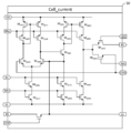
- FIG. 11 is a circuit diagram of a voltage-fixed current detection circuit 50 that detects a current with the potential fixed.
- the detection current from the detection gold electrode 4 of the current sensor cell 23b or the impedance sensor cell 23c is input from the terminal Iin.
- the current flowing through the terminal Iin flows through the cascode connection circuit of the transistors M26P1, M26P5, and M26N1, and is transmitted as current to the array peripheral circuit 60 through the output terminal BC by the current mirrors M26P1, M26P5, M26P2, and M26P3.
- Transistors M26P3, M26P4, M26P7, M26P8, M26N8, M26N9, M26N4, and M26N7 constitute an operation amplifier.
- the gold electrode 4 (terminal Iin) is connected to the gate of one transistor M26N9 of the differential circuit, and the reference voltage GND is input to the gate of the other transistor M26N8.
- the drain of the transistor M26N9 is connected to the gate of the transistor M26N1 of the current mirror circuit.
- FIG. 12 shows a current receiver 61a of the array peripheral circuit 60 to which the current signal BC output from the current sensor cell 23b or the impedance sensor cell 23c is input.
- the input terminal Iin is connected to the output terminal BC of the voltage fixed current detection circuit 50 of FIG.
- the circuit of FIG. 12 obtains the potential of the terminal out to which the current is transferred with the potential of the terminal Iin of the current receiving unit 61a ⁇ fixed.
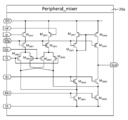
- FIG. 13 shows a current mixer circuit 20a.
- a square wave obtained by shaping the output signal of the AC signal source 31 by the phase shifter 32 and the inverters 33, 34, and 35 is input to the terminals Q and Qb, and signals obtained by inverting H and L are mutually inverted. You are typing.
- the terminal “in” is connected to the output terminal “out” in FIG.
- the product of the difference between the current flowing through the cascode connection circuit of transistors M28P1 and PM28P3 and the current flowing through the cascode connection circuit of transistors M28P2 and M28P4 and the signal input to terminal Q is output to terminal Iout.
- the voltage at the terminal Q is a logic signal and takes two values of H and L, and the voltage at the terminal Qb is an inverted signal of the voltage at the terminal Q.
- the transistors M28N2, N28N3 are turned on, the transistors N28N1, N28N4 are turned off, the current corresponding to the signal at the terminal in flows through the transistor M28N6, the current corresponding to the signal at the terminal ref flows through the transistor M28N5, The differential current is output to the terminal Iout.
- the voltage at terminal Q is L, the current flowing through terminal Iout is inverted.
- a full-wave rectified signal of a signal input from the terminal Iin (FIGS.
- 11 and 12 can be output by inputting a pulse signal having the same cycle as the signal input to the terminal in to the terminal Q. Further, by changing the phase of the voltage at the terminal QI, the amplitude and phase of the input signal from the terminal Iin can be detected.
- this circuit takes the difference between the current corresponding to the signal at the terminal “in” and the current corresponding to the signal at the terminal “ref”, it is possible to reduce noise that enters in common. Since the signal at the terminal Q ⁇ ⁇ ⁇ ⁇ is a logic signal, the amplitude is large and the influence of clock field through is large.
- the configuration of operational transconductance amplifiers of cascode transistors M28P1, M28P2 and folded cascode connections M28P5, M28P6, M28P7, M28P8, M28N5, M28N6, M28N7, M28N9 is adopted.
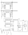
- FIG. 14 shows the voltage / current conversion circuit 40 in FIG. 8, the voltage fixed current detection circuit 50 in FIG. 11, the current receiving unit 61a in FIG. 12, and the same circuit as the reference value inputted from the terminal Iin and the reference output from the terminal out.
- FIG. 14 is a circuit diagram in which a reference receiving unit 61 b ⁇ that outputs ref and the mixer 20 a ⁇ in FIG. 13 are connected.
- the output current of the current sensor cell 23b or the impedance sensor cell 23c that is, the output current of the voltage fixed current detection circuit 50 is converted into a voltage by the current receiving unit 61a and input to the mixer 20a, and the output of the mixer 20a is the current integrating circuit. Output to 20b.
- the current integrating circuit 20b has an operational amplifier 28, a capacitor 26 inserted in the negative feedback circuit, and switches 27 and 30. As a result, the detected current is stored in the capacitor 26 as an electric charge.
- Each voltage at both ends of the capacitor 26 can only take a specific voltage range on the circuit. Therefore, in order to integrate, the capacitor 26 is discharged when the terminal voltage exceeds the set range, and the number of discharges is recorded. There is a need.
- the switch 27 is switched to connect the negative input terminal of the operational amplifier 28 to the constant current source 29, and the charge of the capacitor 26 is extracted.
- the switch 30 is for holding the output voltage of the operational amplifier by connecting the terminal Iout to the GND side at the end of measurement.
- the operational voltage of the operational amplifier 28 is finite, and the upper and lower limits of the output voltage of the operational amplifier 28 are set, and when the upper limit or the lower limit is reached, the capacitor 26 is discharged and the number of discharges is counted.
- the dynamic range of current detection can be increased.
- a mixer 20a, a current integration circuit 20b, an analog-digital conversion circuit 21a, and a parallel-serial conversion circuit 21b are arranged above and below the sensor array 12. As a result, while one side is outputting the detection signal, one side can accumulate the signal, and the integration time can be increased.
- Example 2 is a semiconductor integrated circuit that detects a biological substance by a change in potential, current, and impedance.
- Example 3 has a structure capable of controlling biological materials on a semiconductor substrate as follows.
- FIG. 15 is a photograph showing the semiconductor integrated circuit of Example 3. Any potential stored in advance at any location on the sensor array can be applied to the detection electrode of the sensor. Electrochemical measurement can be performed while controlling biological materials by temperature control and electrophoresis.
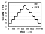
- FIG. 16 shows the result of controlling the temperature on the substrate using the heater 17 and the thermometer 18 on the semiconductor substrate. The actual temperature can accurately follow the measured temperature, and the temperature can be accurately controlled.
- FIG. 17 is a diagram showing a configuration of the semiconductor integrated circuit of FIG.
- the potential held in the voltage holding circuit 38 is applied to the voltage application electrode 37.
- the voltage holding circuit 38 is composed of a sample and hold circuit, and can hold a potential for approximately 10 seconds using a 1 pF capacitor. In order to hold the potential for a long time, the voltage holding circuit 38 is effective to perform a refresh operation and adopt a master / slave configuration so that the potential does not change during sampling.
- the potential of the voltage holding circuit 38 is sequentially stored in the voltage buffer 39 by controlling the X address specifying the address in the X direction, and then transferred to the column specified by the Y address. Thereby, an arbitrary applied voltage can be set to all the detection electrodes 4 ⁇ of the array.
- Electrophoresis is a standard method used in the analysis of biomolecules, but it is performed by applying a voltage close to 1000 V to a distance of 10 cm. When this is performed on a semiconductor substrate, the electrode distance is reduced to 100 ⁇ m, and a low voltage of 1 V is required to obtain the same electric field. In order to maintain the potential by the sample and hold circuit, it is necessary to suppress the photocurrent, and a light shielding environment is required, and an optical detection method cannot be used. For this reason, only an electrical detection method can be used to detect a biological material, and an electrode 4 and a potential detection sensor cell 13 for detecting a potential are provided on the semiconductor integrated circuit. The sensor circuit can also integrate the potential, current, and impedance used in Figure 5 IV.
- the present invention can be applied to a substance measuring apparatus capable of simultaneously measuring various kinds of substances and their physical properties in a short time.
Landscapes
- Chemical & Material Sciences (AREA)
- Health & Medical Sciences (AREA)
- Life Sciences & Earth Sciences (AREA)
- Physics & Mathematics (AREA)
- Immunology (AREA)
- General Physics & Mathematics (AREA)
- Chemical Kinetics & Catalysis (AREA)
- Electrochemistry (AREA)
- Analytical Chemistry (AREA)
- Biochemistry (AREA)
- General Health & Medical Sciences (AREA)
- Pathology (AREA)
- Molecular Biology (AREA)
- Spectroscopy & Molecular Physics (AREA)
- Engineering & Computer Science (AREA)
- Microelectronics & Electronic Packaging (AREA)
- Investigating Or Analyzing Materials By The Use Of Electric Means (AREA)
- Apparatus Associated With Microorganisms And Enzymes (AREA)
Abstract
【課題】対雑音性が高く、多数の物質や多数の物性の特定を短時間で実施できるようにすること。 【解決手段】検出電極により物質に感応して電気信号を出力するセンサユニットがアレイ配列されたセンサアレイと、各センサユニットの出力する電気信号を処理するアレイ周辺回路とを有する半導体集積回路である。センサアレイにおいて、検出電極により検出された電位を電流信号に変換してアレイ周辺回路に出力する電位センサとしてのセンサユニットと、検出電極の電位を固定し、検出電極に流れる電流に相当する電流信号をアレイ周辺回路に出力する電流センサとしてのセンサユニットと、検出電極により検出された交流電流信号をアレイ周辺回路に出力するインピーダンスセンサとしてのセンサユニットとの3種のセンサの内、少なくとも2種のセンサユニットを混在させた。
Description
本発明は、半導体集積回路センサにより電気化学的に溶液内の物質の検出や、物質の物性を測定するための物質物性検出装置(以下、物性を検出する場合も含めて、単に、「物質検出装置」という。)としての半導体集積回路に関する。特に、検出される物質の一例として、DNA 、タンパク質、細胞、バクテリア、ウィルス、グルコース等の生体分子、生体物質等を電位、電流、インピーダンスの変化として電気化学的に検出するための半導体集積回路に関する。
特定の生体分子や生体物質等、又は、それらの物性を検出する物質検出装置は、検出用分子と反応させることにより検出することが多い。例えば、分子が、特定の分子とのみ結合したり、特定の分子とのみ化学反応をおこすことを利用する。この場合、検出精度を向上するために抗体や酵素を介在させることが有効である。また、検出用分子との結合や化学反応を電気信号に変換するには、電位、電流、インピーダンスの変化を検出する電気化学計測法を用いることが多い(特許文献1、4 など)。
また、下記特許文献2によると、電流で物質を検出する場合には定常値に安定するのに時間がかかるために、測定しないセルには一定の固定電圧を印加して、測定セルには固定電圧の印加を遮断して電流を検出することで、各セルの定常電流を高速に順次走査して検出することが行われている。
また、下記特許文献3によると、検出された電圧値を電流パルスに変換してそのパルス幅により物質を検出することが行われている。
また、下記特許文献2によると、電流で物質を検出する場合には定常値に安定するのに時間がかかるために、測定しないセルには一定の固定電圧を印加して、測定セルには固定電圧の印加を遮断して電流を検出することで、各セルの定常電流を高速に順次走査して検出することが行われている。
また、下記特許文献3によると、検出された電圧値を電流パルスに変換してそのパルス幅により物質を検出することが行われている。
その他の従来技術として、例えば、下記非特許文献1では、分子の結合の有無を電荷量の変化として電界効果型トランジスタのゲートを用いて検出する方法が記載されている。下記非特許文献2では、酵素反応を用いて、特定の分子の濃度を酸化体と還元体の濃度比に転写し、酸化還元電位として電界効果型トランジスタのゲートを用いて検出する方法が記載されている。下記非特許文献3では、酵素反応を用いて、特定の分子の濃度を酸化還元電流として検出する方法が記載されている。下記非特許文献4では、特定のウィルスを電極上に設けた抗体により捕獲し、インピーダンスの変化として検出する方法が記載されている。
P. Bergveld, "Thirty years of ISFETOLOGY: What happend in the past 30 years and what may happen in the next 30 years," Sensor and Actuators B 88 (2003) pp. 1-20
Y. Ishige, M. Shimoda, and M. Kamahori, "Extended-gate FET-based enzyme sensor with ferrocenyl-alkanethiol modified gold sensing electrode," Biosens. Bioelectron. 24 (2009) pp. 1096-1102
H. Tanaka, P. Fiorini, S. Peeters, B. Majeed, T. Sterken, M. O. de Beeck, M. Hayashi, H. Yaku, and I. Yamashita,"Sub-micro-liter Electrochemical Single-Nucleotide-Polymorphism Detector for Lab-on-a-Chip System", Japanese Journal of Applied Physics 51 (2012) 04DL02
Y. Ishige, Y. Goto, I. Yanagi, T. Ishida, N. Itabashi, and M. Kamahori, "Feasibility Study on Direct Counting of Viruses and Bacteria by Using Microelectrode Array, " Electroanalysis 4(1) (2012) pp. 131 139
H. Anan, M. Kamahori, Y. Ishige, and K. Nakazato, "Redox-potential sensor array based on extended-gate field-effect transistors with -ferrocenylalkanethiol-modified gold electrodes," Sensors and Actuators B: Chemical, 187, 254-261, 2013
H. Komori, K. Niitsu, J. Tanaka, Y. Ishige, M. Kamahori, and K. Nakazato, "An Extended- Gate CMOS Sensor Array with Enzyme immobilized Microbeads for Redox-Potential Glucose Detection, " BIOCAS 2014
これら電位検出法、電流検出法、インピーダンス検出法は測定対象が異なり、どれか1つを検出するだけでは不十分なことが多い。一例として、DNA の配列を同定する場合、同一塩基が連続して配列しているホモポリマー領域では電流検出が、異なる塩基が配列している非ホモポリマー領域では電位検出が、精度を出すことができる。また、他の一例として、血液検査の項目である血球ヘモグロビン(Hb)は電流検出により、ヘモグロビンA1c(HbA1c)は電位検出により、高精度に測定でき、診断にはHbに対するHbA1c の比率が求められる。
更に、このような物質検出装置は多彩な物質の検出が可能であり、少数多品種となる。半導体集積回路のホトマスク代は、100nm 以下のリソグラフィを用いた場合、1セットあたり1億円を超える。多様な用途に対し、個別に回路を設計していたのでは、チップの単価が高額になりすぎ、普及が限定される。物質検出装置の半導体集積回路においては、電位・電流・インピーダンスのセンサを統合した標準・汎用化が必要である。
しかしながら、従来は、電位検出用のセンサアレイとそのアレイ周辺回路とを集積化したチップ、電流検出用のセンサアレイとそのアレイ周辺回路とを集積化したチップ、さらには、インピーダンス測定用のセンサアレイとその周辺回路とを、個別に設計して、個別のチップに集積していた。また、アレイ周辺回路は、各センサアレイの出力信号の種類が異なるため、それぞれに適したアレイ周辺回路を設計する必要があった。このため、製造コストが増大するという課題があった。また、各センサの出力の種類が一定ではないために、アレイ周辺回路もそれぞれのセンサから出力される周辺回路が必要であった。さらには、チップが異なることから、正確には、同一物質の同一部分での上記3種の測定が同時に実行できるものではなく、出力信号の比率(例えば、電位と電流との比率)が測定すべき特性値である場合に、必ずしも正確ではなかった。このように、従来技術では、高密度化と標準・汎用化を両立することができなかった。
そこで、本発明の目的は、センサユニットからの信号を統一し、センサアレイ周辺回路を統一することにより、高密度な電位・電流・インピーダンス統合型のセンサアレイを実現することにある。
更に、このような物質検出装置は多彩な物質の検出が可能であり、少数多品種となる。半導体集積回路のホトマスク代は、100nm 以下のリソグラフィを用いた場合、1セットあたり1億円を超える。多様な用途に対し、個別に回路を設計していたのでは、チップの単価が高額になりすぎ、普及が限定される。物質検出装置の半導体集積回路においては、電位・電流・インピーダンスのセンサを統合した標準・汎用化が必要である。
しかしながら、従来は、電位検出用のセンサアレイとそのアレイ周辺回路とを集積化したチップ、電流検出用のセンサアレイとそのアレイ周辺回路とを集積化したチップ、さらには、インピーダンス測定用のセンサアレイとその周辺回路とを、個別に設計して、個別のチップに集積していた。また、アレイ周辺回路は、各センサアレイの出力信号の種類が異なるため、それぞれに適したアレイ周辺回路を設計する必要があった。このため、製造コストが増大するという課題があった。また、各センサの出力の種類が一定ではないために、アレイ周辺回路もそれぞれのセンサから出力される周辺回路が必要であった。さらには、チップが異なることから、正確には、同一物質の同一部分での上記3種の測定が同時に実行できるものではなく、出力信号の比率(例えば、電位と電流との比率)が測定すべき特性値である場合に、必ずしも正確ではなかった。このように、従来技術では、高密度化と標準・汎用化を両立することができなかった。
そこで、本発明の目的は、センサユニットからの信号を統一し、センサアレイ周辺回路を統一することにより、高密度な電位・電流・インピーダンス統合型のセンサアレイを実現することにある。
上記課題を解決するための発明は、検出電極により物質に感応して電気信号を出力するセンサユニットがアレイ配列されたセンサアレイと、各センサユニットの出力する電気信号を処理するアレイ周辺回路とを有する半導体集積回路において、センサアレイにおいて、検出電極により検出された電位を電流信号に変換してアレイ周辺回路に出力する電位センサとしてのセンサユニットと、検出電極の電位を固定し、検出電極に流れる電流に相当する電流信号をアレイ周辺回路に出力する電流センサとしてのセンサユニットと、検出電極により検出された交流電流信号をアレイ周辺回路に出力するインピーダンスセンサとしてのセンサユニットとの3種のセンサ(すなわち、電位センサ、電流センサ、インピーダンスセンサ)の内、少なくとも2種のセンサユニットを混在させたことを特徴とする半導体集積回路である。
本発明は、センサによる検出値を電流の大きさとして、センサから出力するようにしたことが特徴である。そして、1チップ上に、電位センサ、電流センサ、インピーダンスセンサの内、少なくとも2種のセンサが混在していることが特徴である。センサアレイ上の領域を2、3分割してそれぞれの領域にそれぞれの種類のセンサユニットを配置させても良い。また、電位センサ、電流センサ、インピーダンスセンサの内の2種、又は、3種のセンサを隣接させて1組センサとして、その1組センサをアレイ配列させることで、センサを混在させても良い。なお、電流センサとインピーダンスセンサとは、構造が同一であっても良い。すなわち、電流センサでインピーダンスセンサを兼用することも可能である。
上記発明において、アレイ周辺回路は、センサアレイを行単位で、順次、選択走査し、選択されたセンサユニットからの電流信号を入力して、その電流信号を処理する回路とすることができる。このアレイ周辺回路もセンサアレイと合わせて1チップ上に集積されている。
また、センサアレイには電位センサと電流センサとが存在し、アレイ周辺回路は、電位センサの出力する電流信号と電流センサの出力する電流信号とを入力し、両電流信号に基づいて物質を測定する回路とすることができる。これにより、例えば、血球の同時測定により、検出電流に対する検出電位の比により血球ヘモグロビン中のヘモグロビンA1c の割合を測定することができる。
また、センサアレイには電位センサと電流センサとが存在し、アレイ周辺回路は、電位センサの出力する電流信号と電流センサの出力する電流信号とを入力し、両電流信号に基づいて物質を測定する回路とすることができる。これにより、例えば、血球の同時測定により、検出電流に対する検出電位の比により血球ヘモグロビン中のヘモグロビンA1c の割合を測定することができる。
また、センサアレイにおいて、電位センサと電流センサとの少なくとも一方と、インピーダンスセンサとが存在しており、アレイ周辺回路は、電位センサの出力する電流信号と電流センサの出力する電流信号との少なくとも一方と、インピーダンスセンサの出力する交流電流信号とに基づいて物質を測定する回路としても良い。これにより、例えば、血球の同時測定により血球の全容積と、その容積に占めるヘモグロビン、ヘモグロビンA1c 、グルコースなどの割合を測定することができる。
また、センサアレイには電位センサが存在し、該電位センサには消費電力の最大値を制御する消費電力制御回路を設けても良い。センサアレイは多数のセンサが存在し、検出用分子との反応は温度に敏感で回路の発熱を避けなければならないことから、省電力化は重要である。
また、アレイ周辺回路は、交流信号を直流信号に変換する検波回路と、検波回路の出力する電流を積分する電流積分回路と、電流積分回路の出力する電流積分信号をディジタル信号に変換するアナログ・ディジタル変換回路とを有する回路とすることができる。交流電流の検出が可能となり、特に、インピーダンスの測定が可能となる。
また、アレイ周辺回路は、交流信号を直流信号に変換する検波回路と、検波回路の出力する電流を積分する電流積分回路と、電流積分回路の出力する電流積分信号をディジタル信号に変換するアナログ・ディジタル変換回路とを有する回路とすることができる。交流電流の検出が可能となり、特に、インピーダンスの測定が可能となる。
また、センサアレイには電位センサが存在し、該電位センサは、検出電極により検出された電気信号を出力するセンサトランジスタを有し、該センサトランジスタに電位検出範囲を定めるソース縮退用トランジスタを接続した構成としても良い。電位検出のダイナミックレンジを拡大することができる。
また、アレイ周辺回路は、検出電極と直接又は他の金属又は絶縁膜を介して接触する溶液の電界、温度を制御する回路を含む構成としても良い。
本発明によると、センサにより検出した値を電流として信号を処理する回路に出力しているので対雑音性を高くすることができる。雑音レベルを電圧出力に比べて3桁ほど低減できる。また、1チップに、電位センサ、電流センサ、インピーダンスセンサの内、少なくとも2種を、センサアレイ上に混在させているので、測定物質の同一部分に対して、各種の物質や物性を短時間で同時に測定でき、得られる情報量が拡大する。また、各センサ出力を電流に統一し、センサアレイ周辺回路を統一することにより、高密度な電位・電流・インピーダンス統合型のセンサアレイを実現することができた。
1 …プリント基板 2 …半導体集積回路チップ 3 …シリコーン・ペースト 4 …金電極5 …ポリイミド 6 …マイクロ流路 7 …PDMS 8 …自己組織化単分子膜 9 …検出用分子 10…ビーズ 11…検出対象分子 12…センサアレイ 13…電位検出センサセル回路 14…出力バッファ 15…校正用切り替えスイッチ 16… Yデコーダ 17…ヒーター 18…温度計
19…アドレスバッファ 20…積分処理部 20a …ミキサ 20b …電流積分回路 21a …アナログ-ディジタル変換回路 21…信号出力部 21b …パラレル入力-シリアル出力シフトレジスタ 22…温度計のプリアンプ 23…センサセル 23a …電位センサセル 23b …電流センサセル 23c …インピーダンスセンサセル 24…クロック発生回路 25…電位検出センサセル回路 25a 25b 25c …センサ回路 26…キャパシタ 27…キャパシタ放電スイッチ 28…オペアンプ 29…キャパシタ放電用電流源 30…サンプル・ホールド切り替えスイッチ 31…交流信号源 32…位相シフター 33,34, 35 …インバータ回路
36… 電圧印可用セルおよびセンサセルのアレイ 37…電圧印可用電極 38…電圧保持回路 39…バッファ 40…電圧電流変換回路 50…電圧固定電流検出回路 60…アレイ周辺回路 61a …電流受信部 61b …基準受信部 80…Si基板 81…ソース領域 82…ドレイン領域 83…ゲート 84…配線層 85…絶縁層 86…トレンチ MaNb(a,b は数字)…NMOS型電界効果型トランジスタ MaPb(a,b は数字)…PMOS型電界効果型トランジスタ
19…アドレスバッファ 20…積分処理部 20a …ミキサ 20b …電流積分回路 21a …アナログ-ディジタル変換回路 21…信号出力部 21b …パラレル入力-シリアル出力シフトレジスタ 22…温度計のプリアンプ 23…センサセル 23a …電位センサセル 23b …電流センサセル 23c …インピーダンスセンサセル 24…クロック発生回路 25…電位検出センサセル回路 25a 25b 25c …センサ回路 26…キャパシタ 27…キャパシタ放電スイッチ 28…オペアンプ 29…キャパシタ放電用電流源 30…サンプル・ホールド切り替えスイッチ 31…交流信号源 32…位相シフター 33,34, 35 …インバータ回路
36… 電圧印可用セルおよびセンサセルのアレイ 37…電圧印可用電極 38…電圧保持回路 39…バッファ 40…電圧電流変換回路 50…電圧固定電流検出回路 60…アレイ周辺回路 61a …電流受信部 61b …基準受信部 80…Si基板 81…ソース領域 82…ドレイン領域 83…ゲート 84…配線層 85…絶縁層 86…トレンチ MaNb(a,b は数字)…NMOS型電界効果型トランジスタ MaPb(a,b は数字)…PMOS型電界効果型トランジスタ
以下、本発明を望ましい実施の形態に基づいて説明する。本件発明は、以下の実施例に限定されるものではない。
図1に、半導体集積回路センサにより構成された物質検出装置の例を示す。プリント基板1 の上に7.5mm 角の半導体集積回路チップ2 をダイボンディングし、ワイヤボンディングにより電気的接続をした後、ワイヤ部分をシリコーン・ペースト3 で封止する。半導体集積回路チップ2 の表面に血液や唾液、採取水等を流し、生体物質を半導体基板に集積されたセンサ回路により計測する。半導体集積回路チップ2 は数千から数千万のセンサセルを含み、数千から数千万の検出を同時並行的に行う。例えば、ウィルスの塩基数は数百万で構成されており、数千万のセンサセルで同時並行的に塩基を検出することにより10分でウィルスの全遺伝子情報を得ることができる。
図2は本装置のセンサユニットの構成を示し、その装置を用いた生体物質の検出の1 例を示した図で、図2(A) は1 つのセンサセルの断面模式図、図2(B) は2次元アレイ配列された複数のセンサセルの平面顕微鏡写真である。半導体集積回路チップ2 には電子回路が形成され、最上層の配線層には検出電極である金電極4 が形成される。80はSi基板、81はソース領域、82はドレイン領域、83はゲートで、これらにより電界効果トランジスタ(以下、「FET 」という)が構成されている。84は金電極4 とゲート83とを接続する配線層、85は絶縁層である。金はイオン化傾向が低く、溶液に接しても安定な金属である。なお、電極の金属は金以外であっても良い。基板表面は保護膜としてポリイミド5 およびSU-8( ネガティブフォトレジストの一種であり、以下、単に、「SU-8」という) から成るマイクロ流路6 が設けられ、その上に比較的大きな流路を形成したポリジメチルシロキサン「PDMS」 7が密着される。
金電極4 の汚染を防ぐため、金電極4 上に自己組織化単分子膜8 を設ける。SU-8から成るマイクロ流路 6によりセンサ上にトレンチ86を形成し、酵素や抗体、プライマー等の検出用分子9 を直径10ミクロン程度のビーズ10に固定し、トレンチ86内に入れる。調べたい検体11はビーズ上の検出用分子9 と化学反応を起こし、その結果を電位の変化としてFET により検出する。ビーズ10が金電極4 を覆うと化学反応物質が金電極4 に供給されなくなる弊害がある。これを避けるために、図2(A) 、(B) に示すように、トレンチ86の開口面に垂直な中心軸と金電極4 の面に垂直な中心軸とが一致しないように、トレンチ86と金電極4 の配置をずらしている。
この構成を用いて血液中のグルコースを酸化還元電位により検出した結果が、本発明者らにより非特許文献5 および非特許文献6 に報告されている。そこでは検出用分子9 としてヘキソキナーゼ(hexokinase)、グルコース-6-リン酸デヒドロゲナーゼ(Glucose-6-phosphate dehydrogenase) 、ジアホラーゼ(Diaphorase)の 3酵素が1つのビーズにアビジン-ビオチン結合を用いて固定され、自己組織化単分子膜8 として 11-フェロセニル-1- ウンデカンチオール(11-FUT)を用いている。
図3は、半導体集積回路チップ2 上に設けられたセンサアレイ12を示す写真である。図3(B) はセンサアレイ12の1 部を拡大した顕微鏡写真であり、セル毎に、金属電極4 が存在する。この回路では64x64 個のセンサが2 次元アレイ配設され、同時並行して4096種類のバイオ反応による電位の変化を検出することができる。バイオ反応に伴い金電極4 上の電位が変化し、この変化から生体分子を検出する。この例ではセンサセルは60um x 60um 、金電極の開口部は20um x 20um の大きさを持つ。
図4は、半導体集積回路チップ2 と外部インターフェース回路の構成を示す。図4において、2 は半導体集積回路チップ、4 は金電極、13は電位センサセル回路( 電位センサ) 、14は出力バッファ、15は較正用切り替えスイッチである。13には特許文献1の電位検出型センサと、電流検出センサ又はインピーダンスセンサとが用いられる。信号はバッファ回路14を通して出力しているが、バッファ回路以降の閾値ばらつき等による誤差を補正するため、スイッチ15を通して外部から電圧を加えてその結果を測定し較正する。これにより、誤差を5mV から0.5mV 以下の1/10以下に低減している。
図5は電位、電流、インピーダンスの変化を同時に検出するセンサアレイ12を集積した半導体集積回路チップ2 の写真である。実施例2の装置は、全体構成は、図1、2と同一である。図5において、16はセンサアレイ12の1 行を選択するY デコーダ、17は半導体集積回路チップの温度を変えるヒーター、18はチップの温度を測る温度計、19はアレイの1 行を選択する場所を記憶しておくアドレスバッファ、20はセンサセルからの電流信号を外部から入力される交流信号とミキシングするミキサ20a 及びそのミキサ20a の出力を積分する電流積分回路20b とから成る積分処理部である。21は電流積分回路から出力されたアナログ信号をディジタル信号に変換するアナログ-ディジタル変換回路21a とディジタル信号を外部に順次送るためのパラレル入力-シリアル出力シフトレジスタ21b(以下、「パラシリ変換回路」という) から成る信号出力部、22は温度計18の出力を増幅するプリアンプ、23はセンサセル、24はクロック発生回路である。アレイ周辺回路60( 図6) は、Y デコーダ16、アドレスバッファ19、ミキサ20a と電流積回路20b とから成る積分処理部20、アナログ-ディジタル変換回路21a とパラシリ変換回路21b から成る信号出力部21、クロック発生回路24などで構成されている。
半導体基板には電位、電流、インピーダンスを検出するセンサセル23が、32x32 の1024個の2 次元アレイ配列されている。電位センサである電位センサセル23a 、電流センサである電流センサセル23b 、インピーダンスセンサであるインピーダンスセンサセル23c がが隣接されて、2 次元アレイ配列されている。ただし、インピーダンスセンサセル23c は交流電流を検出するので、本実施例では、電流センサセル23b はインピーダンスセンサセル23c を兼用している。したがって、ある特定の電流センサセル23b は電流を検出し、他のある特定の電流センサセル23b はインピーダンスセンサセル23c となり、インピーダンスを測定する。勿論、インピーダンスセンサセル23c を電流センサセル23b と構造の異なるセンサセルとして別に独立して設けても良い。また、センサアレイ12の周辺部に、1 行につき1つのY デコーダ16が、1 列につき上下2つの積分処理部20、信号出力部21とが集積されている。更に、配線(ヒータ)17、温度計18、温度計のプリアンプ22により、基板の温度を室温から120 ℃まで設定することができる。
化学反応の時間は通常数ミリ秒の長さで、これは集積回路の処理時間の6 桁長い。検出時間を高速に行う利点はなく、長い時間を有効に使って精度を向上させることが有効である。精度を向上させる方法として、単発の信号を用いるのではなく、積算した信号を用いて信号を平均化する。電流は電荷量の時間微分であるので、キャパシタに電荷として蓄えることにより、電流の積算を行うことができる。電位を積算するには、一旦、電流に置き換え、キャパシタに電荷として蓄える。
図6は、図5の電位、電流、インピーダンスの検出回路に関するブロック図である。図6において、電位センサセル23a は検出電位を電流に変換する電圧電流変換回路40を有し、電流センサセル23b とインピーダンスセンサセル23c は、電圧固定電流検出回路50を有している。アレイ周辺回路60はミキサ20a 、電流積分回路20b 、アナログ-ディジルタ変換回路21a 、パラシリ変換回路21b とを有している。電圧電流変換回路40及び電圧固定電流検出回路50の出力は共に電流信号としてアレイ周辺回路60に入力される。インピーダンスセンサセル23c の出力するインピーダンス検出信号は交流電流であり、ミキサ20a により平滑化される。その後段の電流積分回路20b はローパスフィルタの役割をする。電位は各センサセル23内で電流に変換してアレイ周辺回路60で積算する。この構成をとることにより、電位、電流、インピーダンスの信号を1つのアレイ周辺回路60で処理することができる。
なお、ミキサ20a はインピーダンスの検出において、交流信号を平滑化して直流信号に変換するもので、電位検出、電流検出においては、交流信号源31の周波数を0Hz 、すなわち定電圧源とする。あるいは数Hzから数kHz の低周波信号を与え、ロックインアンプとして用い、雑音を低減することもできる。
なお、ミキサ20a はインピーダンスの検出において、交流信号を平滑化して直流信号に変換するもので、電位検出、電流検出においては、交流信号源31の周波数を0Hz 、すなわち定電圧源とする。あるいは数Hzから数kHz の低周波信号を与え、ロックインアンプとして用い、雑音を低減することもできる。
図7に半導体集積回路の構成を示す。図5、6で説明した回路と同一の回路は同一符号が付されている。電位センサセル23a のセンサ回路25aは次に述べる電圧電流変換回路(開路電圧センサ)であり、電流センサセル23b のセンサ回路25b とインピーダンスセンサセル23c のセンサ回路25c は、電圧固定電流検出回路(閉路電流センサ)である。検出信号はアナログ-ディジタル変換回路21a 、パラシリ変換回路21b を介して、シリアルディジタル信号として外部に出力される。アナログ-ディジタル変換回路21a としては、例えばデュアルスロープ型や電流モード・デルタ-シグマ方式等を用いる。
図8は電圧電流変換型の電位センサセル23a の回路図であり、定電圧Bpp, BBpは図9のセルバイアス回路により供給される。図8の電位センサセル23a の回路に流れる最大電流は、図9の定電圧Bnにより決まる。図9の出力Bpは次段のセルバイアス回路のBnに接続することにより、設定値を伝えることができる。Bnを次段のBnと接続する構成では配線による電圧降下により誤差が生じるが、このように電流として伝えることにより、正確に設定値を伝えることができる。
図8では、検出電圧の範囲を3 倍に拡げるため、2 段のソース縮退トランジスタ(ダイオード)M23N2, M23N3, M23N4, M23N5を設けている。トランジスタM23N1 のゲートに金電極4(検出電極)の電位(Vin )が印加される。この検出電位Vin は、トランジスタM23N1, M23N2, M23N4 に流れるドレイン電流に変換される。このような構成をとることにより、負荷電流によりソース電位が上昇して、電圧に対する感度が1/3 に低減され、検出電圧の範囲を3 倍に拡大させている。
トランジスタM23N7 のゲートは、トランジスタN23N6 のソースに接続されており、トランジスタN23N6 のゲートは、トランジスタM23N7 のドレインに接続されている。トランジスタM23N7 はトランジスタM23N1 を飽和領域に保つために、トランジスタM23N6 はトランジスタM23N7 を飽和領域に保つためのトランジスタである。この回路の特長は入力電圧Vin が大きくなっても、トランジスタM23P1, M23P4, M23N6, M23N1, M23N2, M23N4のカスコード接続から成る電流検出回路を流れる電流が、トランジスタM23P2, M23P5, M23N7, M23N3, M23N5 のカスコード接続から成る電流制限回路を流れる電流Iss 以上にはならないことである。電流制限回路を流れる電流Iss は定電圧Bn(Bn により決定されるBpp,BBp)により決定され、その電流Iss によりトランジスタM23N3, M23N5のゲート-ソース間電圧VGSsが定まる。検出電位Vin が3VGSs より大きくなるとM23N1 が線形領域(トライオード領域)に入るため、トランジスタM23P1, M23P4, M23N6, M23N1, M23N2, M23N4の電流検出回路を流れる電流はIss を超えることはない。
これにより定電圧Bnにより回路の消費電力の上限を設定できる。バイオ反応は温度に敏感であり、半導体集積回路の消費電力が大きいと発熱し、温度を上昇させ、正確に生体分子の量を同定することができなくなる。温度上昇を無視できる半導体集積回路の消費電力は1mW/cm2 以下であり、千のセンサセルを集積した場合、1つのセンサセルに流せる電流を1uA 以下に制限する必要がある。
図8において、BCは電位センサセル23a の出力端子でアレイ周辺回路60の入力端子に接続される。アレイ周辺回路60により端子BCの電圧はGND と同一の電圧に保たれる。トランジスタM23P7 とトランジスタM23N8 は一方がオンの場合には他方はオフとなるようにそれぞれのゲート電圧により制御される相補形の出力回路である。端子BCからの出力信号は検出電位が電流に変換された電流信号である。電位センサセル23a からの電流を読む場合には、トランジスタM23P7 をオンに、トランジスタM23N8 をオフにする。電位センサセル23a の電流を読まない場合には、トランジスタM23P7 をオフに、トランジスタM23N8 をオンにすることで、トランジスタM23P6 のドレイン電圧が常にGND の電圧に保たれるようにする。このようにして、電圧を常に一定に保つことにより、雑音低減と高速化を図っている。
図10は図8、9の回路の電流電圧特性の測定結果である。 BCは電位センサセル23a の出力端子BCの電流、 DDは回路全体に流れる電流である。a, b, c, d, e.f はそれぞれ端子Bnの電圧2V, 1.8V, 1.6V, 1.4V, 1.2V, 1Vに対応している。端子Bnの電圧を1.6Vに設定することにより2V近い広い検出範囲を得るとともに、検出電位Vin が高くなっても回路の電流 DDに2uA の上限を設定することができる。
電圧電流変換回路40ではトランジスタの閾値ばらつきの影響を受ける。閾値のばらつきを校正するため、図8の回路においてトランジスタM23N9 を設けて、検出電位Vin が入力されない状態で、基準電圧BSをトランジスタM23N1 に印加して、電位センサセル23a の出力電流BCの較正ができるようにしている。
図11は電位を固定した状態で電流を検出する電圧固定電流検出回路50の回路図である。電流センサセル23b 又はインピーダンスセンサセル23c の検出金電極4 からの検出電流は端子Iin から入力される。端子Iin に流れる電流は、トランジスタM26P1,M26P5,M26N1 のカスコート接続回路を流れ、カレントミラーM26P1, M26P5, M26P2, M26P3により、出力端子BCを通してアレイ周辺回路60に電流として伝えられる。トランジスタM26P3, M26P4, M26P7, M26P8, M26N8, M26N9, M26N4, M26N7は作動アンプを構成している。差動回路の一方のトランジスタM26N9 のゲートには金電極4(端子Iin)が接続され、他方のトランジスタM26N8 のゲートには基準電圧GND が入力している。トランジスタM26N9 のドレインは、カレントミラー回路のトランジスタM26N1 のゲートに接続されている。この差動アンプにより、端子Iin と端子GND の電圧差を増幅して、ソースフォロワとして働くトランジスタM26N1 に負帰還をかけることにより、金属電極4(端子Iin)の電圧が一定に固定される。
この電流センサセル23b 又はインピーダンスセンサセル23c から出力される電流信号BCを入力するアレイ周辺回路60の電流受信部61a を図12に示す。入力端子Iin が図11の電圧固定電流検出回路50の出力端子BCに接続されている。図12の回路により、電流受信部61a の端子Iin の電位を固定した状態で電流を移す端子out の電位を得ている。
図13は電流のミキサ回路20a である。端子Q と端子Qbには、交流信号源31の出力信号が位相シフター32、インバータ33、34、35により成形されて得られる方形波が入力しており、相互にH 、L が反転した信号が入力している。端子inは図12の出力端子out に接続されている。トランジスタM28P1, M28P3のカスコード接続回路を流れる電流と、トランジスタM28P2, M28P4のカスコード接続回路を流れる電流との差と、端子Q に入力される信号との積の電流を端子Ioutに出力する。端子Q の電圧はロジック信号でH, Lの2 値をとり、端子Qbの電圧は端子Q の電圧の反転信号である。端子Q の電圧がH のときにはトランジスタM28N2, N28N3がオン、トランジスタN28N1, N28N4がオフとなり、端子inの信号に対応した電流がトランジスタM28N6 に、端子ref の信号に対応した電流がトランジスタM28N5 に流れ、差分電流が端子Ioutに出力される。端子Q の電圧がL のときには端子Ioutに流れる電流が反転する。端子inに入力される信号と同じ周期のパルス信号を端子Q に入力させることにより端子Iin (図11、図12)から入力される信号の全波整流信号を出力することができる。また、端子Q の電圧の位相を変えることにより、端子Iin からの入力信号の振幅と位相を検出することができる。
また、この回路は端子inの信号に対応した電流と端子ref の信号に対応した電流の差分をとるため、共通に入る雑音を削減することができる。端子Q の信号はロジック信号であるため振幅が大きくクロックフィールドスルーの影響が大きい。これを緩和するため、カスコード・トランジスタM28P1, M28P2および折り返しカスコード接続M28P5,M28P6, M28P7, M28P8, M28N5, M28N6, M28N7, M28N9 のオペレーショナル・トランスコンダクタンス・アンプの構成をとる。
図14は図8の電圧電流変換回路40、図11の電圧固定電流検出回路50、図12の電流受信部61a と、それと同一回路で端子Iin から基準値を入力して、端子out から基準出力ref を出力する基準受信部61b と、図13のミキサ20a とを接続した回路図である。電流センサセル23b 又はインピーダンスセンサセル23c の出力電流、すなわち、電圧固定電流検出回路50の出力電流は、電流受信部61a により電圧に変換されて、ミキサ20a に入力され、ミキサ20a の出力が電流積分回路20b に出力される。電流積分回路20b は、オペアンプ28と負帰還回路に挿入されたキャパシタ26と、スイッチ27、30を有している。これにより検出電流は、キャパシタ26に電荷として蓄えられる。
キャパシタ26の両端の各電圧は、回路上、特定の電圧範囲しかとることができないため、積算をするには、キャパシタ26の端子電圧が設定範囲を超えたときに放電し、放電回数を記録する必要がある。キャパシタ26を放電するには、スイッチ27を切り替えてオペアンプ28の負入力端子を定電流源29に接続し、キャパシタ26の電荷を引き抜く。スイッチ30は、測定終了時に、端子IoutをGND 側に接続してオペアンプの出力電圧をホールドするためのものである。
オペアンプ28の動作電圧は有限であり、オペアンプ28の出力電圧の上限と下限を設定し、上限もしくは下限に達したときに、キャパシタ26の電荷を放電するとともに、その放電回数をカウントすることにより、電流検出のダイナミックレンジを大きくすることができる。
また、図5の半導体集積回路はセンサアレイ12の上下にミキサ20a 、電流積分回路20b 、アナログ-ディジタル変換回路21a とパラシリ変換回路21b とを配している。これにより、片方が検出信号を出力している間に片方が信号を積算することができ、積算時間を長くとることが可能になる。
また、図5の半導体集積回路はセンサアレイ12の上下にミキサ20a 、電流積分回路20b 、アナログ-ディジタル変換回路21a とパラシリ変換回路21b とを配している。これにより、片方が検出信号を出力している間に片方が信号を積算することができ、積算時間を長くとることが可能になる。
実施例2は、電位、電流、インピーダンスの変化により生体物質を検出する半導体集積回路である。実施例3は、以下のように、生体物質の制御も半導体基板上で行うようにできる構造を有している。図15は、実施例3の半導体集積回路を示した写真である。センサアレイ上の任意の場所において、予め記憶された任意の電位を、センサの検出電極に印可することができる。温度制御と電気泳動により生体物質を制御しながら電気化学計測をおこなうことができる。
温度によりPCR (ポリメラーゼ連鎖反応)にみられるように分子の増幅を行うことができる。また、検出信号の精度を高めるには温度の制御が有効である。サンプル溶液とサンプル洗浄液を交互に半導体基板に供給した場合、2つの溶液に温度差があると、温度差による信号の変化が加わることになる。これを除去するには、測定前にチップ上で溶液の温度を一定にすることが有効である。図16は半導体基板上のヒーター17と温度計18を用いて基板上の温度を制御した結果を示す。実際の温度は測定温度に正確に追従できており、温度が正確に制御できている。
図17は図15の半導体集積回路の構成を示した図である。電圧保持回路38に保持された電位が電圧印加用電極37に印可される。電圧保持回路38はサンプル・ホールド回路からなり、1pF のキャパシタを用いて、おおよそ10秒間、電位を保持することができる。電圧保持回路38は、長時間、電位を保持するには、リフレッシュ動作を行い、サンプリング時に電位が変化しないようにマスター・スレーブ構成をとることが有効である。
電圧保持回路38の電位は、X 方向のアドレスを指定するX address を制御することで電圧バッファ(voltage buffer)39に一列分逐次記憶された後、Y address で指定した列に移される。これにより、アレイのすべての検出電極4 に任意の印可電圧を設定することができる。
生体分子の分析において電気泳動は標準的に用いられている方法であるが、10cmの距離に1000V 近い電圧を印可して行う。これを半導体基板で行う場合、電極距離は100 umに縮小され、同じ電界を得るのに1Vの低電圧で済む。サンプル・ホールド回路により電位を保つには光電流を抑える必要があり、遮光環境が必要で、光学的検出法を用いることができない。このため生体物質を検出するには、電気的検出法しか用いることができず、半導体集積回路上には、電位を検出する電極4 と電位検出センサセル13が設けられている。センサ回路は図5 で用いた電位、電流、インピーダンスを統合することも可能である。
本発明は、多種類の物質やその物性を短時間で同時に測定できる物質測定装置に応用できる。
Claims (8)
- 検出電極により物質に感応して電気信号を出力するセンサユニットがアレイ配列されたセンサアレイと、各センサユニットの出力する電気信号を処理するアレイ周辺回路とを有する半導体集積回路において、
前記センサアレイにおいて、
前記検出電極により検出された電位を電流信号に変換して前記アレイ周辺回路に出力する電位センサとしてのセンサユニットと、
前記検出電極の電位を固定し、前記検出電極に流れる電流に相当する電流信号をアレイ周辺回路に出力する電流センサとしてのセンサユニットと、
前記検出電極により検出された交流電流信号を前記アレイ周辺回路に出力するインピーダンスセンサとしてのセンサユニットと
の3種のセンサの内、少なくとも2種のセンサユニットを混在させた
ことを特徴とする半導体集積回路 - 前記アレイ周辺回路は、前記センサアレイを行単位で、順次、選択走査し、選択されたセンサユニットからの前記電流信号を入力して、その電流信号を処理する回路であることを特徴とする請求項1に記載の半導体集積回路。
- 前記センサアレイには前記電位センサと前記電流センサとが存在し、
前記アレイ周辺回路は、前記電位センサの出力する電流信号と前記電流センサの出力する電流信号とを入力し、両電流信号に基づいて前記物質を測定する回路であることを特徴とする請求項1又は請求項2に記載の半導体集積回路。 - 前記センサアレイにおいて、前記電位センサと前記電流センサとの少なくとも一方と、前記インピーダンスセンサとが存在しており、
前記アレイ周辺回路は、前記電位センサの出力する電流信号と前記電流センサの出力する電流信号との少なくとも一方と、前記インピーダンスセンサの出力する前記交流電流信号とに基づいて前記物質を測定する回路であることを特徴とする請求項1又は請求項2に記載の半導体集積回路。 - 前記センサアレイには電位センサが存在し、該電位センサには消費電力の最大値を制御する消費電力制御回路を有することを特徴とする請求項1乃至請求項4の何れか1項に記載の半導体集積回路。
- 前記アレイ周辺回路は、
交流信号を直流信号に変換する検波回路と、
検波回路の出力する電流を積分する電流積分回路と、
電流積分回路の出力する電流積分信号をディジタル信号に変換するアナログ・ディジタル変換回路と
を有することを特徴とする請求項1乃至請求項5の何れか1項に記載の半導体集積回路。 - 前記センサアレイには電位センサが存在し、該電位センサは、前記検出電極により検出された電気信号を出力するセンサトランジスタを有し、該センサトランジスタに電位検出範囲を定めるソース縮退用トランジスタを接続したことを特徴とする請求項1乃至請求項6の何れか1項に記載の半導体集積回路。
- 前記アレイ周辺回路は、前記検出電極と直接又は他の金属又は絶縁膜を介して接触する溶液の電界、温度を制御する回路を含むことを特徴とする請求項1乃至請求項7の何れか1項に記載の半導体集積回路。
Applications Claiming Priority (2)
| Application Number | Priority Date | Filing Date | Title |
|---|---|---|---|
| JP2015045373 | 2015-03-07 | ||
| JP2015-045373 | 2015-03-07 |
Publications (1)
| Publication Number | Publication Date |
|---|---|
| WO2016143320A1 true WO2016143320A1 (ja) | 2016-09-15 |
Family
ID=56880026
Family Applications (2)
| Application Number | Title | Priority Date | Filing Date |
|---|---|---|---|
| PCT/JP2016/056849 Ceased WO2016143705A1 (ja) | 2015-03-07 | 2016-03-04 | 参照電極保持部材及び物質検出装置 |
| PCT/JP2016/001212 Ceased WO2016143320A1 (ja) | 2015-03-07 | 2016-03-04 | 半導体集積回路 |
Family Applications Before (1)
| Application Number | Title | Priority Date | Filing Date |
|---|---|---|---|
| PCT/JP2016/056849 Ceased WO2016143705A1 (ja) | 2015-03-07 | 2016-03-04 | 参照電極保持部材及び物質検出装置 |
Country Status (3)
| Country | Link |
|---|---|
| US (1) | US20180180566A1 (ja) |
| JP (1) | JP6539918B2 (ja) |
| WO (2) | WO2016143705A1 (ja) |
Cited By (1)
| Publication number | Priority date | Publication date | Assignee | Title |
|---|---|---|---|---|
| JP2020500317A (ja) * | 2016-11-07 | 2020-01-09 | ディーエヌエーイー・ダイアグノスティックス・リミテッド | Chemfetアレイ |
Families Citing this family (4)
| Publication number | Priority date | Publication date | Assignee | Title |
|---|---|---|---|---|
| US11150215B2 (en) * | 2017-09-28 | 2021-10-19 | International Business Machines Corporation | Microfluidic device with laterally insertable electrodes |
| WO2019099855A1 (en) * | 2017-11-17 | 2019-05-23 | Siemens Healthcare Diagnostics Inc. | Sensor assembly and method of using same |
| US20200138512A1 (en) * | 2018-11-06 | 2020-05-07 | Biosense Webster (Israel) Ltd. | Attaining Higher Impedances for Large Indifferent Electrodes |
| JP7573620B2 (ja) * | 2020-01-13 | 2024-10-25 | ベックマン コールター, インコーポレイテッド | 固体イオン選択電極 |
Citations (6)
| Publication number | Priority date | Publication date | Assignee | Title |
|---|---|---|---|---|
| JPH1194793A (ja) * | 1997-09-22 | 1999-04-09 | Research Institute Of Innovative Technology For The Earth | 光走査型二次元濃度分布測定装置 |
| JP2003315295A (ja) * | 2002-04-22 | 2003-11-06 | Matsushita Electric Works Ltd | 水分量センサ |
| JP2003322630A (ja) * | 2002-05-01 | 2003-11-14 | Seiko Epson Corp | バイオセンサ、バイオセンシングシステム、及びバイオセンシング方法 |
| JP2010025728A (ja) * | 2008-07-18 | 2010-02-04 | Funai Electric Advanced Applied Technology Research Institute Inc | 物質検出装置及び携帯電話機 |
| JP2013064746A (ja) * | 2006-12-14 | 2013-04-11 | Life Technologies Corp | 大規模fetアレイを用いた分析物測定のための方法および装置 |
| JP2013220066A (ja) * | 2012-04-17 | 2013-10-28 | Hitachi Ltd | センサチップ及びそれを用いた測定方法 |
Family Cites Families (10)
| Publication number | Priority date | Publication date | Assignee | Title |
|---|---|---|---|---|
| US5019238A (en) * | 1984-03-28 | 1991-05-28 | Baxter Diagnostics Inc. | Means for quantitative determination of analyte in liquids |
| US4627893A (en) * | 1984-03-28 | 1986-12-09 | Amdev, Inc. | Means and methods for quantitative determination of analyte in liquids |
| JPS61169756A (ja) * | 1985-01-23 | 1986-07-31 | Hitachi Ltd | 比較電極装置 |
| JPH06148124A (ja) * | 1992-11-12 | 1994-05-27 | Hitachi Ltd | ディスポーザブルイオンセンサユニット |
| JP3419691B2 (ja) * | 1998-09-04 | 2003-06-23 | 日本電信電話株式会社 | 極微少量フローセル、及びその製造方法 |
| CN101158664A (zh) * | 2002-07-31 | 2008-04-09 | 株式会社东芝 | 碱基序列检测装置及碱基序列自动解析装置 |
| JP2006242900A (ja) * | 2005-03-07 | 2006-09-14 | Mitsubishi Chemicals Corp | センサユニット及び反応場セルユニット並びに分析装置 |
| US8349167B2 (en) * | 2006-12-14 | 2013-01-08 | Life Technologies Corporation | Methods and apparatus for detecting molecular interactions using FET arrays |
| US8673627B2 (en) * | 2009-05-29 | 2014-03-18 | Life Technologies Corporation | Apparatus and methods for performing electrochemical reactions |
| US9274059B2 (en) * | 2011-03-14 | 2016-03-01 | Battelle Memorial Institute | Microfluidic electrochemical device and process for chemical imaging and electrochemical analysis at the electrode-liquid interface in-situ |
-
2016
- 2016-03-04 US US15/556,576 patent/US20180180566A1/en not_active Abandoned
- 2016-03-04 WO PCT/JP2016/056849 patent/WO2016143705A1/ja not_active Ceased
- 2016-03-04 JP JP2017505309A patent/JP6539918B2/ja active Active
- 2016-03-04 WO PCT/JP2016/001212 patent/WO2016143320A1/ja not_active Ceased
Patent Citations (6)
| Publication number | Priority date | Publication date | Assignee | Title |
|---|---|---|---|---|
| JPH1194793A (ja) * | 1997-09-22 | 1999-04-09 | Research Institute Of Innovative Technology For The Earth | 光走査型二次元濃度分布測定装置 |
| JP2003315295A (ja) * | 2002-04-22 | 2003-11-06 | Matsushita Electric Works Ltd | 水分量センサ |
| JP2003322630A (ja) * | 2002-05-01 | 2003-11-14 | Seiko Epson Corp | バイオセンサ、バイオセンシングシステム、及びバイオセンシング方法 |
| JP2013064746A (ja) * | 2006-12-14 | 2013-04-11 | Life Technologies Corp | 大規模fetアレイを用いた分析物測定のための方法および装置 |
| JP2010025728A (ja) * | 2008-07-18 | 2010-02-04 | Funai Electric Advanced Applied Technology Research Institute Inc | 物質検出装置及び携帯電話機 |
| JP2013220066A (ja) * | 2012-04-17 | 2013-10-28 | Hitachi Ltd | センサチップ及びそれを用いた測定方法 |
Cited By (2)
| Publication number | Priority date | Publication date | Assignee | Title |
|---|---|---|---|---|
| JP2020500317A (ja) * | 2016-11-07 | 2020-01-09 | ディーエヌエーイー・ダイアグノスティックス・リミテッド | Chemfetアレイ |
| JP7144432B2 (ja) | 2016-11-07 | 2022-09-29 | ディーエヌエーイー・ダイアグノスティックス・リミテッド | Chemfetアレイ |
Also Published As
| Publication number | Publication date |
|---|---|
| JPWO2016143705A1 (ja) | 2017-12-21 |
| JP6539918B2 (ja) | 2019-07-10 |
| WO2016143705A1 (ja) | 2016-09-15 |
| US20180180566A1 (en) | 2018-06-28 |
Similar Documents
| Publication | Publication Date | Title |
|---|---|---|
| JP4883812B2 (ja) | 物質検出装置 | |
| Schienle et al. | A fully electronic DNA sensor with 128 positions and in-pixel A/D conversion | |
| Manickam et al. | A CMOS Electrochemical Biochip With 32$\times $32 Three-Electrode Voltammetry Pixels | |
| EP2619564B1 (en) | Matched pair transistor circuits | |
| US9086400B2 (en) | Amplifier and array for measuring small current | |
| Jafari et al. | Nanostructured CMOS wireless ultra-wideband label-free PCR-free DNA analysis SoC | |
| WO2016143320A1 (ja) | 半導体集積回路 | |
| JP4731544B2 (ja) | 生体分子検出装置及びそれを用いた生体分子検出方法 | |
| JP4407790B2 (ja) | 電子装置及びその駆動方法並びに電子回路の駆動方法 | |
| Ghafar-Zadeh et al. | CMOS capacitive sensors for lab-on-chip applications | |
| Garner et al. | A multichannel DNA SoC for rapid point-of-care gene detection | |
| JP2023525267A (ja) | ナノポア単分子シーケンシングのためのシステム及び装置 | |
| KR20150013128A (ko) | 단일 뉴클레오티드 다형성 검출용 isfet 어레이 | |
| Chang et al. | CMOS ion sensitive field effect transistors for highly sensitive detection of DNA hybridization | |
| US20210018464A1 (en) | Nanopore device and methods of detecting and classifying charged particles using same | |
| Genco et al. | A 4× 4 biosensor array with a 42-μw/channel multiplexed current sensitive front-end featuring 137-DB DR and zeptomolar sensitivity | |
| Singh | From sensors to systems: CMOS-integrated electrochemical biosensors | |
| JP2015210233A (ja) | 超並列的生体分子検出方法および装置 | |
| US6922081B2 (en) | Electronic circuit, sensor arrangement and method for processing a sensor signal | |
| Hassibi et al. | A programmable electrochemical biosensor array in 0.18/spl mu/m standard CMOS | |
| Das et al. | High-throughput nanopore-FET array readout IC with 5-MHz bandwidth and background offset/drift calibration | |
| Prathap et al. | ISFET Pixel Array with selectable sensitivity and bulk-based offset-drift nullification capability for reduction of non-ideality effects | |
| Hefele et al. | Integrated multipurpose analog front-end for electrochemical ISFET sensors | |
| Majji et al. | Ion Sensitive Field Effect Transistor as a Bio-compatible Device: A Review | |
| Lai et al. | Biosensor integrated with transducer to detect the glucose |
Legal Events
| Date | Code | Title | Description |
|---|---|---|---|
| 121 | Ep: the epo has been informed by wipo that ep was designated in this application |
Ref document number: 16761294 Country of ref document: EP Kind code of ref document: A1 |
|
| NENP | Non-entry into the national phase |
Ref country code: DE |
|
| NENP | Non-entry into the national phase |
Ref country code: JP |
|
| 122 | Ep: pct application non-entry in european phase |
Ref document number: 16761294 Country of ref document: EP Kind code of ref document: A1 |