WO2016143229A1 - 窒化物半導体積層体の製造方法及び窒化物半導体積層体 - Google Patents
窒化物半導体積層体の製造方法及び窒化物半導体積層体 Download PDFInfo
- Publication number
- WO2016143229A1 WO2016143229A1 PCT/JP2015/085824 JP2015085824W WO2016143229A1 WO 2016143229 A1 WO2016143229 A1 WO 2016143229A1 JP 2015085824 W JP2015085824 W JP 2015085824W WO 2016143229 A1 WO2016143229 A1 WO 2016143229A1
- Authority
- WO
- WIPO (PCT)
- Prior art keywords
- layer
- nitride semiconductor
- gan
- gan layer
- substrate
- Prior art date
- Legal status (The legal status is an assumption and is not a legal conclusion. Google has not performed a legal analysis and makes no representation as to the accuracy of the status listed.)
- Ceased
Links
Images
Classifications
-
- H—ELECTRICITY
- H10—SEMICONDUCTOR DEVICES; ELECTRIC SOLID-STATE DEVICES NOT OTHERWISE PROVIDED FOR
- H10P—GENERIC PROCESSES OR APPARATUS FOR THE MANUFACTURE OR TREATMENT OF DEVICES COVERED BY CLASS H10
- H10P14/00—Formation of materials, e.g. in the shape of layers or pillars
- H10P14/20—Formation of materials, e.g. in the shape of layers or pillars of semiconductor materials
- H10P14/32—Formation of materials, e.g. in the shape of layers or pillars of semiconductor materials characterised by intermediate layers between substrates and deposited layers
- H10P14/3242—Structure
- H10P14/3256—Microstructure
-
- C—CHEMISTRY; METALLURGY
- C30—CRYSTAL GROWTH
- C30B—SINGLE-CRYSTAL GROWTH; UNIDIRECTIONAL SOLIDIFICATION OF EUTECTIC MATERIAL OR UNIDIRECTIONAL DEMIXING OF EUTECTOID MATERIAL; REFINING BY ZONE-MELTING OF MATERIAL; PRODUCTION OF A HOMOGENEOUS POLYCRYSTALLINE MATERIAL WITH DEFINED STRUCTURE; SINGLE CRYSTALS OR HOMOGENEOUS POLYCRYSTALLINE MATERIAL WITH DEFINED STRUCTURE; AFTER-TREATMENT OF SINGLE CRYSTALS OR A HOMOGENEOUS POLYCRYSTALLINE MATERIAL WITH DEFINED STRUCTURE; APPARATUS THEREFOR
- C30B29/00—Single crystals or homogeneous polycrystalline material with defined structure characterised by the material or by their shape
- C30B29/10—Inorganic compounds or compositions
- C30B29/38—Nitrides
-
- H—ELECTRICITY
- H10—SEMICONDUCTOR DEVICES; ELECTRIC SOLID-STATE DEVICES NOT OTHERWISE PROVIDED FOR
- H10P—GENERIC PROCESSES OR APPARATUS FOR THE MANUFACTURE OR TREATMENT OF DEVICES COVERED BY CLASS H10
- H10P14/00—Formation of materials, e.g. in the shape of layers or pillars
- H10P14/20—Formation of materials, e.g. in the shape of layers or pillars of semiconductor materials
- H10P14/29—Formation of materials, e.g. in the shape of layers or pillars of semiconductor materials characterised by the substrates
- H10P14/2901—Materials
- H10P14/2921—Materials being crystalline insulating materials
-
- H—ELECTRICITY
- H10—SEMICONDUCTOR DEVICES; ELECTRIC SOLID-STATE DEVICES NOT OTHERWISE PROVIDED FOR
- H10P—GENERIC PROCESSES OR APPARATUS FOR THE MANUFACTURE OR TREATMENT OF DEVICES COVERED BY CLASS H10
- H10P14/00—Formation of materials, e.g. in the shape of layers or pillars
- H10P14/20—Formation of materials, e.g. in the shape of layers or pillars of semiconductor materials
- H10P14/32—Formation of materials, e.g. in the shape of layers or pillars of semiconductor materials characterised by intermediate layers between substrates and deposited layers
- H10P14/3202—Materials thereof
- H10P14/3214—Materials thereof being Group IIIA-VA semiconductors
- H10P14/3216—Nitrides
-
- H—ELECTRICITY
- H10—SEMICONDUCTOR DEVICES; ELECTRIC SOLID-STATE DEVICES NOT OTHERWISE PROVIDED FOR
- H10P—GENERIC PROCESSES OR APPARATUS FOR THE MANUFACTURE OR TREATMENT OF DEVICES COVERED BY CLASS H10
- H10P14/00—Formation of materials, e.g. in the shape of layers or pillars
- H10P14/20—Formation of materials, e.g. in the shape of layers or pillars of semiconductor materials
- H10P14/32—Formation of materials, e.g. in the shape of layers or pillars of semiconductor materials characterised by intermediate layers between substrates and deposited layers
- H10P14/3242—Structure
- H10P14/3244—Layer structure
- H10P14/3251—Layer structure consisting of three or more layers
-
- H—ELECTRICITY
- H10—SEMICONDUCTOR DEVICES; ELECTRIC SOLID-STATE DEVICES NOT OTHERWISE PROVIDED FOR
- H10P—GENERIC PROCESSES OR APPARATUS FOR THE MANUFACTURE OR TREATMENT OF DEVICES COVERED BY CLASS H10
- H10P14/00—Formation of materials, e.g. in the shape of layers or pillars
- H10P14/20—Formation of materials, e.g. in the shape of layers or pillars of semiconductor materials
- H10P14/34—Deposited materials, e.g. layers
- H10P14/3402—Deposited materials, e.g. layers characterised by the chemical composition
- H10P14/3414—Deposited materials, e.g. layers characterised by the chemical composition being group IIIA-VIA materials
- H10P14/3416—Nitrides
-
- H—ELECTRICITY
- H10—SEMICONDUCTOR DEVICES; ELECTRIC SOLID-STATE DEVICES NOT OTHERWISE PROVIDED FOR
- H10P—GENERIC PROCESSES OR APPARATUS FOR THE MANUFACTURE OR TREATMENT OF DEVICES COVERED BY CLASS H10
- H10P14/00—Formation of materials, e.g. in the shape of layers or pillars
- H10P14/20—Formation of materials, e.g. in the shape of layers or pillars of semiconductor materials
- H10P14/36—Formation of materials, e.g. in the shape of layers or pillars of semiconductor materials characterised by treatments done before the formation of the materials
-
- H—ELECTRICITY
- H10—SEMICONDUCTOR DEVICES; ELECTRIC SOLID-STATE DEVICES NOT OTHERWISE PROVIDED FOR
- H10P—GENERIC PROCESSES OR APPARATUS FOR THE MANUFACTURE OR TREATMENT OF DEVICES COVERED BY CLASS H10
- H10P14/00—Formation of materials, e.g. in the shape of layers or pillars
- H10P14/20—Formation of materials, e.g. in the shape of layers or pillars of semiconductor materials
- H10P14/32—Formation of materials, e.g. in the shape of layers or pillars of semiconductor materials characterised by intermediate layers between substrates and deposited layers
- H10P14/3242—Structure
-
- H—ELECTRICITY
- H10—SEMICONDUCTOR DEVICES; ELECTRIC SOLID-STATE DEVICES NOT OTHERWISE PROVIDED FOR
- H10P—GENERIC PROCESSES OR APPARATUS FOR THE MANUFACTURE OR TREATMENT OF DEVICES COVERED BY CLASS H10
- H10P14/00—Formation of materials, e.g. in the shape of layers or pillars
- H10P14/20—Formation of materials, e.g. in the shape of layers or pillars of semiconductor materials
- H10P14/38—Formation of materials, e.g. in the shape of layers or pillars of semiconductor materials characterised by treatments done after the formation of the materials
Definitions
- the present invention relates to a method for manufacturing a nitride semiconductor multilayer body and a nitride semiconductor multilayer body.
- a gallium nitride (GaN) substrate as a self-supporting substrate, for example, a VAS method (Void-assisted Method) is sometimes used.
- a self-standing substrate is formed by forming a GaN layer as a self-supporting substrate on a base substrate and peeling the base substrate and the GaN layer.
- a first GaN layer provided on the substrate As the base substrate, a first GaN layer provided on the substrate, an aluminum gallium nitride (AlGaN) layer provided on the first GaN layer, and a second GaN layer provided on the AlGaN layer, And a metal film (for example, a TiN film) provided on the second GaN layer, and the second GaN layer and the metal film are made porous by forming voids.
- a physical semiconductor laminate may be used (see, for example, Patent Document 1).
- the first GaN layer, the AlGaN layer, and the second GaN layer are each formed (film formation, growth) by a MOVPE (Metal Organic Vapor Phase Epitaxy) method.
- MOVPE Metal Organic Vapor Phase Epitaxy
- each layer included in the nitride semiconductor multilayer body By forming each layer included in the nitride semiconductor multilayer body by the MOVPE method, pits appearing on the surface of the second GaN layer, for example, even if the thickness of the first GaN layer is reduced to about 2 to 3 ⁇ m. Macro defects can be sufficiently reduced.
- the growth rate of the nitride semiconductor by the MOVPE method is as low as several ⁇ m / hour at most, there is a problem that when each layer is formed by the MOVPE method, the productivity of the nitride semiconductor stacked body becomes very low. As a result, the productivity of free standing substrates by the VAS method may be reduced.
- the present invention uses a HVPE (Hydride Vapor Phase Epitaxy) method with a growth rate of several to several tens of mm / hour, which is higher than the MOVPE method, to form a free-standing substrate by the VAS method.
- An object of the present invention is to provide a technique for improving the productivity of a nitride semiconductor laminated body used as a base substrate and the productivity of a free-standing substrate.
- a nitride semiconductor stacked body in which a force is applied to the first gallium nitride layer so that the warp generated in the first gallium nitride layer is canceled by the warp generated in the aluminum nitride layer.
- the present invention it is possible to provide a technique for improving the productivity of a nitride semiconductor stacked body used as a base substrate when forming a freestanding substrate by the VAS method, and the productivity of a freestanding substrate.
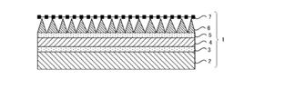
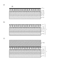
- the longitudinal cross-sectional schematic of the nitride semiconductor laminated body concerning one Embodiment of this invention is shown. It is a figure which shows an example of the manufacturing process of the nitride semiconductor laminated body concerning one Embodiment of this invention, and a GaN self-supporting substrate.
- each layer of the nitride semiconductor laminate is not grown by the MOVPE method, which is slower than the MOVPE method. It is considered to form (film formation) by a high growth rate, for example, HVPE.
- HVPE high growth rate
- the HVPE method is inferior in crystal growth controllability compared to the MOVPE method. Therefore, for example, when the first GaN layer having a thickness of about 2 to 3 ⁇ m as described above is formed by the HVPE method, a pit having a diameter of slightly less than 1 ⁇ m to several ⁇ m appears on the surface (upper surface) of the second GaN layer. In some cases, it is not possible to sufficiently reduce such macro defects. As a result, the metal film provided on the second GaN layer may be peeled off. For example, the metal film may be peeled off when the metal film is formed by vapor deposition, or the metal film may be peeled off during the process of modifying the metal film into a porous film.
- the yield of the nitride semiconductor substrate may be lowered. That is, even when each layer of the nitride semiconductor multilayer body is formed by the HVPE method, the productivity of the nitride semiconductor multilayer body may be reduced.
- the thickness of the first GaN layer is made thicker than when the GaN layer is formed by the MOVPE method.
- the thickness of the first GaN layer may be 4 ⁇ m or more.
- a nitride semiconductor multilayer body having a substrate and a predetermined nitride semiconductor (nitride semiconductor layer) including the first GaN layer may be greatly warped.
- a nitride semiconductor laminate formed by providing a predetermined nitride semiconductor on a 2 inch substrate typically has a warpage amount at room temperature when the thickness of the first GaN layer is 4 ⁇ m. Becomes 60 ⁇ m or more. The origin of this warp is due to the difference between the thermal expansion coefficient of the nitride semiconductor and the thermal expansion coefficient of sapphire as the substrate.
- the amount of warpage is almost zero at around 1000 ° C., which is the temperature (growth temperature) for growing each layer constituting the nitride semiconductor multilayer body. .
- a nitride semiconductor laminate having a large warp at room temperature is used as the base substrate, for example, a GaN layer (hereinafter referred to as “GaN layer” to be a self-supporting substrate on the base substrate.
- the base substrate (nitride semiconductor laminate) may be cracked when forming (film formation)). Most of the cracks in the base substrate occur during the temperature rising process from room temperature to 1000 ° C. which is the growth temperature.
- a nitride semiconductor multilayer body including a nitride semiconductor having a large strain, that is, a nitride semiconductor multilayer body greatly warped at room temperature tends to be easily broken.
- the crack is also taken over by the GaN free-standing substrate formed on the base substrate, so that the growth yield of the GaN free-standing substrate layer is reduced, that is, the productivity of the GaN free-standing substrate is reduced. .
- the present inventors have provided a nitride semiconductor stack with a layer that warps in a direction opposite to the direction of warpage that occurs in the first GaN layer, so that the nitride semiconductor can be used even when the HVPE method is used. It has been found that the warpage occurring in the entire laminate can be reduced.
- the present invention is based on the above findings found by the inventors.
- the nitride semiconductor multilayer body 1 includes a substrate 2.
- a substrate made of sapphire, silicon, SiC, langasite, zirconium diboride, or gallium arsenide (GaAs) can be used.
- GaAs gallium arsenide
- a sapphire substrate is more preferably used as the substrate 2 from the viewpoint of lattice constants of an AlN layer 3 and a GaN layer (first GaN layer 4 and second GaN layer 6) described later.
- An AlN layer 3 is provided on any main surface of the substrate 2.
- the AlN layer 3 is warped.
- the AlN layer 3 is warped such that the center (center portion) is the lowest. That is, the AlN layer 3 warps, for example, a concave shape (a bowl shape).
- the thickness of the AlN layer 3 is a thickness that can sufficiently warp the AlN layer 3.
- the thickness of the AlN layer 3 is preferably 10 nm or more and 500 nm or less, for example.
- the AlN layer 3 may not be sufficiently warped. By making the thickness of the AlN layer 3 10 nm or more, the AlN layer 3 can be sufficiently warped.
- the thickness of the AlN layer 3 exceeds 500 nm, it takes time to form the AlN layer 3 even when the AlN layer 3 is formed by the HVPE method. May decrease.
- the thickness of the AlN layer 3 500 nm or less this can be solved, and the decrease in productivity of the nitride semiconductor multilayer body 1 can be suppressed.
- the AlN layer 3 also functions as a buffer layer that buffers a mismatch in lattice constant between the sapphire substrate and the first GaN layer 4 described later.
- the first GaN layer 4 is provided on the AlN layer 3.
- the first GaN layer 4 functions as an underlayer for the second GaN layer 6 described later, and the dislocation of the second GaN layer 6 can be reduced.
- the first GaN layer 4 is warped.
- the first GaN layer 4 is warped such that the center (center portion) is the highest. That is, the first GaN layer 4 is warped to have a convex shape (dome shape), for example.
- the first GaN layer 4 is warped in the opposite direction to the warp generated in the AlN layer 3.
- the thickness of the first GaN layer 4 is preferably 4 ⁇ m or more, for example.
- the first GaN layer 4 is formed by, for example, the HVPE method
- if the thickness of the first GaN layer 4 is less than 4 ⁇ m macros such as pits appearing on the surface (upper surface) of the second GaN layer 6 described later. Defects may not be reduced sufficiently.
- the macro defect density on the surface of the second GaN layer 6 may not be sufficiently reduced.
- the first GaN layer 4 is warped in the opposite direction to the warp generated in the AlN layer 3. Accordingly, the warping of the AlN layer 3 can apply a force to the first GaN layer 4 so as to cancel the warp generated in the first GaN layer 4. That is, a force in a direction opposite to the direction of warpage generated in the first GaN layer 4, for example, a force that flattens the first GaN layer 4 can be applied to the first GaN layer. Further, when the first GaN layer 4 is warped, a force can be applied to the AlN layer 3 so as to cancel the warp generated in the AlN layer 3.
- a force in a direction opposite to the direction of warping generated in the AlN layer 3, for example, a force that flattens the AlN layer 3 can be applied to the AlN layer 3.
- the AlN layer 3 and the first GaN layer 4 are warped, so that a force that cancels the warpage generated in each layer can be applied to each layer.
- the warp generated in the first GaN layer 4 by the warp generated in the AlN layer 3 can be offset. As a result, the amount of warpage (stress) in the entire nitride semiconductor multilayer body 1 can be reduced.
- a group III nitride semiconductor layer 5 containing aluminum (Al) is provided on the first GaN layer 4.
- the group III nitride semiconductor layer 5 has voids in the first GaN layer 4 when a process for modifying the metal film 7 described later into a porous film (hereinafter also simply referred to as “modification process”) is performed. It functions as a layer (void formation preventing layer) that prevents (void) from being formed.
- the group III nitride semiconductor layer 5 functions as a layer that suppresses desorption of N (nitrogen element) from the first GaN layer 4 due to the modification treatment.
- the group III nitride semiconductor layer 5 also functions as a layer that suppresses the enlargement of voids formed in the second GaN layer 6 described later.
- group III nitride semiconductor layer 5 containing Al for example, a layer having a composition of Al x Ga 1-x N (0.01 ⁇ x ⁇ 1) is preferably provided.
- Voids are also formed in the group III nitride semiconductor layer 5 by the modification process described later.
- a void penetrating in the thickness direction may be formed in the group III nitride semiconductor layer 5 in some cases. That is, a through hole may be formed in the group III nitride semiconductor layer 5.
- the group III nitride semiconductor layer 5 may not function as a void formation suppression layer. That is, during the modification process described later, the first GaN layer 4 is also exposed to the first GaN layer 4 through the portion of the first GaN layer 4 exposed from the through hole formed in the group III nitride semiconductor layer 5. Voids may be formed.
- the value of x may be 1. That is, an AlN layer may be provided as the group III nitride semiconductor layer 5. However, from the viewpoint of reducing the difference in lattice constant between the group III nitride semiconductor layer 5, the first GaN layer 4, and the second GaN layer 6 described later, the group III nitride semiconductor layer 5 is x More preferably, an AlGaN layer having a value of less than 1 is provided.
- the thickness of the group III nitride semiconductor layer 5 is preferably formed to a thickness at which no through hole is formed in the group III nitride semiconductor layer 5 by a modification process described later.
- the thickness of the group III nitride semiconductor layer 5 is preferably 3 nm or more.
- the thickness of the group III nitride semiconductor layer 5 is less than 3 nm, through holes may be formed in the group III nitride semiconductor layer 5 by a modification process described later.
- the thickness of group III nitride semiconductor layer 5 is set to 3 nm or more, formation of a through hole in group III nitride semiconductor layer 5 can be more reliably suppressed by a modification process described later.
- the upper limit of the thickness of the group III nitride semiconductor layer 5 is not particularly limited. However, as the thickness of the group III nitride semiconductor layer 5 increases, strain due to lattice mismatch between the group III nitride semiconductor layer 5 containing Al and the first GaN layer 4 increases, and the group III nitride semiconductor layer When growing 5, the group III nitride semiconductor layer 5 may be cracked. Therefore, the thickness of group III nitride semiconductor layer 5 is preferably set to a thickness (critical film thickness) or less that does not cause a crack corresponding to the composition of group III nitride semiconductor layer 5.
- a second GaN layer 6 having a predetermined thickness (for example, several 100 nm) is provided. Voids are formed in the second GaN layer 6 by a modification process described later. That is, the second GaN layer 6 is a porous layer.
- a metal film 7 is provided on the second GaN layer 6. Voids are formed in the metal film 7. That is, the metal film 7 is a porous film.
- the metal contained in the metal film 7 include titanium, vanadium, chromium, manganese, iron, cobalt, nickel, copper, yttrium, zirconium, niobium, molybdenum, tellurium, ruthenium, rhodium, palladium, hafnium, tantalum, and tungsten. , Rhenium, osmium, iridium, platinum, gold and the like can be used.
- a titanium nitride (TiN) film is provided as the metal film 7, for example.
- the thickness of the metal film 7 is preferably 100 nm or less, for example, and more preferably 30 nm or less. If the thickness of the metal film 7 exceeds 100 nm, it takes time to modify the metal film 7 into a porous film, and the productivity of the nitride semiconductor multilayer body 1 may be reduced. By setting the thickness of the metal film 7 to 100 nm or less, this can be solved, and the decrease in productivity of the nitride semiconductor multilayer body 1 can be further suppressed. By reducing the thickness of the metal film 7 to 30 nm or less, it is possible to further suppress a decrease in productivity of the nitride semiconductor multilayer body 1.
- the lower limit of the thickness of the metal film 7 is not particularly limited, but is preferably 1 nm or more, for example.
- First step A first step of forming the AlN layer 3 on the substrate 2 (for example, on the sapphire substrate) is performed.
- the AlN layer 3 is formed by the HVPE method using a hydride vapor phase epitaxy (HVPE) apparatus.
- HVPE hydride vapor phase epitaxy
- the formation temperature (growth temperature) of the AlN layer 3 is preferably set to a temperature at which the dense AlN layer 3 can be formed.
- the growth temperature of the AlN layer 3 is preferably 800 ° C. or higher and 1200 ° C. or lower, and more preferably about 1000 ° C.
- the AlN layer 3 may not be a dense layer. As a result, when the temperature of the AlN layer 3 drops, the AlN layer 3 may not be sufficiently warped.
- the AlN layer 3 By setting the growth temperature of the AlN layer 3 to 800 ° C. or higher, the AlN layer 3 can be made sufficiently dense. As a result, the AlN layer 3 can be sufficiently warped.
- the growth temperature of the AlN layer 3 exceeds 1200 ° C., the surface of the sapphire substrate becomes rough before the AlN layer 3 grows. For this reason, the crystal orientation of the AlN layer grown on the surface of the sapphire substrate may be lowered.
- the growth temperature of the AlN layer 3 By setting the growth temperature of the AlN layer 3 to 1200 ° C. or less, it is possible to prevent the crystal orientation of the AlN layer 3 from being lowered.
- the thickness of the AlN layer 3 is, for example, not less than 10 nm and not more than 500 nm.
- a second step of forming the first GaN layer 4 on the AlN layer 3 is performed.
- the first GaN layer 4 is formed by HVPE using an HVPE apparatus.
- the thickness of the first GaN layer 4 is preferably 4 ⁇ m or more.
- the thickness of the first GaN layer 4 can be adjusted, for example, by adjusting the film formation time of the first GaN layer 4.
- a third step of forming a group III nitride semiconductor layer 5 containing Al on the first GaN layer 4 is performed.
- group III nitride semiconductor layer 5 is formed by HVPE using an HVPE apparatus.
- the group III nitride semiconductor layer 5 for example, a layer having a composition of Al x Ga 1-x N (0.01 ⁇ x ⁇ 1) is preferably formed.
- the thickness of the group III nitride semiconductor layer 5 is preferably 3 nm or more. The thickness of group III nitride semiconductor layer 5 can be adjusted, for example, by adjusting the film formation time of group III nitride semiconductor layer 5.
- a fourth step of forming the second GaN layer 6 having a predetermined thickness on the group III nitride semiconductor layer 5 is performed.
- the second GaN layer 6 is formed by HVPE using an HVPE apparatus.
- a fifth step of forming a metal film 7 having a predetermined thickness on the second GaN layer 6 is performed.
- a Ti film as the metal film 7 is formed by vapor deposition, for example. Thereby, for example, a stacked body 1A shown in FIG. 2A is formed.
- a sixth step of modifying the second GaN layer 6 and the metal film 7 to be porous is performed.
- heat treatment is performed on the second GaN layer 6 and the metal film 7.
- a void is formed in the second GaN layer 6 to be modified into a porous layer
- a void is formed in the metal film 7 (metal nitride film) by modifying the metal film 7 into a metal nitride film.
- the metal film 7 is modified into a porous film.
- the nitride semiconductor multilayer body 1 shown in FIG. 2B is formed.
- a seventh step of forming a free-standing substrate by the VAS method is performed. That is, in the seventh step, as shown in FIG. 2C, after the sixth step is finished, the nitride semiconductor multilayer body 1 is used as a base substrate, and a GaN layer that becomes a free-standing substrate on the base substrate. 10 (GaN free-standing substrate layer 10) is formed, and a GaN free-standing substrate is formed. Specifically, first, in the seventh step, the substrate 2, the AlN layer 3, the first GaN layer 4, the group III nitride semiconductor layer 5, the second GaN layer 6, and the metal film 7.
- a GaN free-standing substrate layer 10 is formed on a base substrate (porous metal film 7 (metal nitride film)) using a nitride semiconductor laminate 1 having Thereafter, the GaN free-standing substrate layer 10 is peeled from the base substrate. Note that the GaN free-standing substrate layer 10 is naturally peeled from the underlying substrate when the stacked body of the underlying substrate and the GaN free-standing substrate layer 10 is cooled to a predetermined temperature (for example, about room temperature). The peeled GaN free-standing substrate layer 10 becomes a GaN free-standing substrate.
- the seventh step it is preferable to adjust the growth time of the GaN layer so that the GaN free-standing substrate layer 10 has a predetermined thickness (for example, 800 ⁇ m).
- the GaN free-standing substrate layer 10 separated from the base substrate may be sliced to a predetermined thickness. That is, a plurality of GaN free-standing substrates may be formed from one GaN free-standing substrate layer 10.
- AlN layer 3 that generates a warp in a direction opposite to the direction of the warp that occurs in the first GaN layer 4 is provided, and the AlN layer 3 and the first GaN layer 4 are warped, respectively. Even when each of the GaN layer 4, the group III nitride semiconductor layer 5, and the second GaN layer 6 is formed by the HVPE method, the amount of warpage can be reduced in the entire nitride semiconductor multilayer body 1. it can. As a result, the productivity of the nitride semiconductor multilayer body 1 and the productivity of the GaN free-standing substrate can be improved.
- each of the AlN layer 3, the first GaN layer 4, the group III nitride semiconductor layer 5, and the second GaN layer 6 is formed by the HVPE method, so that the growth rate of each layer is increased. Can be made 10 to 100 times faster than when formed by the MOVPE method, for example.
- the nitride semiconductor multilayer body 1 can be formed in a time of 1 hour or less including the time until the reactor cleaning after growing the above-described layers. Therefore, the productivity of the nitride semiconductor multilayer body 1 can be improved as compared with the case where the above-described layers are formed by the MOVPE method.
- the nitride semiconductor multilayer body 1 in which a predetermined layer is formed by the HVPE method is used as the base substrate. Even when it is used as a substrate, it is possible to prevent the base substrate (nitride semiconductor multilayer body 1) from being broken (cracked) during the formation of the GaN layer (GaN free-standing substrate layer 10) serving as a free-standing substrate. can do. Thereby, the yield (growth yield) of the GaN free-standing substrate layer 10 can be improved. As a result, the productivity of the GaN free-standing substrate can be improved.
- the dense AlN layer 3 can be formed by forming the AlN layer 3 in an atmosphere of high temperature (for example, 800 ° C. or more and 1200 ° C. or less). Thereby, when the temperature of the AlN layer 3 falls, the AlN layer 3 can be warped more sufficiently. Therefore, even when the thickness of the first GaN layer 4 is increased and the amount of warpage generated in the first GaN layer 4 is increased, the amount of warpage in the entire nitride semiconductor multilayer body 1 is reliably reduced. be able to. As a result, the effects (c) and (d) can be obtained more.
- high temperature for example, 800 ° C. or more and 1200 ° C. or less
- the growth temperature of the AlN layer 3 can be brought close to the growth temperature of the first GaN layer 4.
- the growth temperature of the AlN layer 3 and the growth temperature of the first GaN layer 4 can be made comparable.
- time until it starts a 2nd process can be shortened.
- the waiting time until the temperature of the processing chamber provided in the HVPE apparatus is raised (or lowered) to a predetermined temperature at which the first GaN layer 4 can be formed is shortened. be able to.
- the formation of the first GaN layer 4 can be started immediately after the formation of the AlN layer 3 is completed. Therefore, the productivity of the nitride semiconductor multilayer body 1 can be further improved.
- the macro defects can be sufficiently reduced.
- the macro defect density on the surface of the second GaN layer 6 can be less than 2 cm ⁇ 2 , preferably 0 cm ⁇ 2 .
- the nitride semiconductor multilayer body 1 forms a base substrate when a GaN free-standing substrate is formed by, for example, the VAS method.
- the nitride semiconductor multilayer body 1 can function as a good base substrate. Thereby, the productivity of the GaN free-standing substrate can be further improved.
- a GaN free-standing substrate with good reproducibility that is, a high-quality GaN free-standing substrate can be formed by the VAS method.
- the invention according to this embodiment is particularly effective when the thickness of the first GaN layer 4 cannot be reduced, that is, when the thickness of the first GaN layer 4 needs to be increased. is there.
- the amount of warpage generated in the first GaN layer 4 increases.
- the AlN layer 3 as in the present embodiment, even when the amount of warpage generated in the first GaN layer 4 is large, the amount of warpage in the entire nitride semiconductor multilayer body 1 is reduced. be able to.
- the entire nitride semiconductor multilayer body 1 can have a warp amount of less than 60 ⁇ m. Thereby, the effects (c) and (d) can be further obtained.
- the first GaN layer is formed by, for example, the MOVPE method.
- the thickness of the first GaN layer is about 2 to 3 ⁇ m, macro defects appearing on the surface of the second GaN layer can be sufficiently reduced. That is, the thickness of the first GaN layer can be made thinner than when the first GaN layer is formed by the HVPE method. As a result, the amount of warpage generated in the first GaN layer is also reduced. Therefore, when the first GaN layer is formed by the MOVPE method, the amount of warpage in the entire nitride semiconductor multilayer body is provided without providing the AlN layer 3 that causes warpage in the opposite direction to the warpage generated in the first GaN layer.
- the productivity of the nitride semiconductor stacked body becomes very poor.
- the time until reactor cleaning after growing each layer including the first GaN layer it may take about 10 hours to form the nitride semiconductor stacked body.
- a predetermined layer such as the first GaN layer 4 is formed by the HVPE method, so that the time required for forming the nitride semiconductor multilayer body 1 is about 1 hour.
- the productivity of the nitride semiconductor multilayer body 1 can be greatly improved.
- the seventh step of forming the GaN free-standing substrate is considered to be included in the manufacturing process of the nitride semiconductor multilayer body 1 is described, but the present invention is not limited to this. That is, in the seventh step, the first to sixth steps may be manufacturing steps of the nitride semiconductor multilayer body 1, and the seventh step may be a manufacturing step of the GaN free-standing substrate.
- the present invention is not limited to this.
- the slice process may not be performed. That is, one self-standing substrate may be formed from one GaN free-standing substrate layer 10.
- Samples 8 to 14 are nitride semiconductor laminates formed in the same manner as Samples 1 to 7, respectively, except that the AlN layer was not provided.
- a thickness of 20 nm is grown between the sapphire substrate and the first GaN layer 4 under a low temperature (550 ° C.) condition instead of the AlN layer.
- GaN layer low temperature growth GaN layer
- the thicknesses of the first GaN layers of the samples 8 to 14 are as shown in Table 2 below.
- the warpage amount was measured for each of the nitride semiconductor laminates of Samples 1 to 14. The results are shown in Table 1 and Table 2, respectively.
- the yield was calculated for each nitride semiconductor multilayer body of Samples 1 to 14. This yield is the yield when a GaN free-standing substrate is formed using the nitride semiconductor laminate as a base substrate. We also observed the main causes of defects that caused the yield to decrease. These results are shown in Table 1 and Table 2, respectively.
- “TiN peeling” indicates that the TiN film, which is a metal film, has been peeled off.
- “cracking” means that when the GaN free-standing substrate layer is formed on the nitride semiconductor multilayer body, the nitride semiconductor multilayer body is cracked and the GaN free-standing substrate itself is defective. ing.
- the amount of warpage generated in the nitride semiconductor multilayer body can be reduced by providing the film.
- the amount of warpage of the nitride semiconductor stacked body of sample 4 provided with the AlN layer is 33 ⁇ m.
- the amount of warpage of the nitride semiconductor multilayer body of Sample 11 in which the AlN layer was not provided was 60 ⁇ m.
- the nitride semiconductor multilayer structure is provided by providing an AlN layer that warps in a direction opposite to the direction of warpage generated in the first GaN layer. It was confirmed that the amount of warpage can be reduced in the whole body. For example, it was confirmed that the amount of warpage can be less than 60 ⁇ m in the entire nitride semiconductor multilayer body.
- the yield can be improved by reducing the amount of warpage of the entire nitride semiconductor multilayer body.
- the yield of the sample 5 having a smaller warpage amount in the entire nitride semiconductor multilayer body is higher. Confirmed that it was high. That is, it was confirmed that a decrease in productivity of the nitride semiconductor multilayer body can be suppressed.
- the thickness of the first GaN layer is 4 ⁇ m or more, the macro defect density appearing on the surface of the second GaN layer can be sufficiently reduced. It was confirmed. For example, when the thickness of the first GaN layer is 4 ⁇ m or more from each of Samples 4 to 7 and Samples 11 to 14, the macro defect density on the surface of the second GaN layer can be reduced to 0 cm ⁇ 2. confirmed.
- Appendix 2 The method for producing a nitride semiconductor multilayer body according to appendix 1, preferably, In the first step, the temperature for forming the aluminum nitride layer is set to 800 ° C. or more and 1200 ° C. or less.
- Appendix 3 The method for producing a nitride semiconductor stacked body according to appendix 1 or 2, preferably, In the first step, the thickness of the aluminum nitride layer is set to 10 nm or more and 500 nm or less.
- Appendix 4 A method for producing a nitride semiconductor multilayer structure according to any one of appendices 1 to 3, preferably, In the second step, the first gallium nitride layer is set to 4 ⁇ m or more.
- Appendix 5 A method for manufacturing a nitride semiconductor multilayer structure according to any one of appendices 1 to 4, preferably, A sapphire substrate is used as the substrate.
- Appendix 6 A method for manufacturing a nitride semiconductor multilayer structure according to any one of appendices 1 to 5, preferably, A seventh step of forming a gallium nitride layer serving as a self-supporting substrate on the metal film modified to be porous;
- Appendix 7 The method for manufacturing a nitride semiconductor multilayer body according to appendix 6, preferably, In the seventh step, the gallium nitride layer to be the self-supporting substrate is peeled from the metal film to form the self-supporting substrate.
- Appendix 8 The method for manufacturing a nitride semiconductor multilayer body according to appendix 7, preferably, In the seventh step, a plurality of the self-supporting substrates are formed from one gallium nitride layer serving as the self-standing substrate by performing a slicing process on the separated gallium nitride layer serving as the self-supporting substrate.
- a nitride semiconductor stacked body in which a force is applied to the first gallium nitride layer so that the warp generated in the first gallium nitride layer is canceled by the warp generated in the aluminum nitride layer.
- Appendix 10 The nitride semiconductor stacked body according to appendix 9, preferably, The thickness of the first gallium nitride layer is 4 ⁇ m or more.
- Appendix 12 The nitride semiconductor stacked body according to any one of appendices 9 to 11, preferably, The substrate is a sapphire substrate.
Landscapes
- Chemical & Material Sciences (AREA)
- Inorganic Chemistry (AREA)
- Engineering & Computer Science (AREA)
- Crystallography & Structural Chemistry (AREA)
- Materials Engineering (AREA)
- Metallurgy (AREA)
- Organic Chemistry (AREA)
- Crystals, And After-Treatments Of Crystals (AREA)
Abstract
基板上にAlN層を形成する第1の工程と、AlN層上に第1のGaN層を形成する第2の工程と、第1のGaN層上に、Alを含むIII族窒化物半導体層を形成する第3の工程と、III族窒化物半導体層上に、第2のGaN層を形成する第4の工程と、第2のGaN層上に、金属膜を形成する第5の工程と、第2のGaN層及び金属膜を多孔質に改質する処理を行う第6の工程と、を有し、第1~第4の各工程をそれぞれ、HVPE法により行う。
Description
本発明は、窒化物半導体積層体の製造方法及び窒化物半導体積層体に関する。
従来より、自立基板としての窒化ガリウム(GaN)基板の形成方法として、例えばVAS法(Void-assisted Method)が用いられることがある。VAS法では、下地基板上に自立基板となるGaN層を形成し、下地基板とGaN層とを剥離することで自立基板が形成される。この下地基板として、基板上に設けられた第1のGaN層と、第1のGaN層上に設けられた窒化アルミニウムガリウム(AlGaN)層と、AlGaN層上に設けられた第2のGaN層と、第2のGaN層上に設けられた金属膜(例えばTiN膜)と、を備え、第2のGaN層及び金属膜が、空隙(ボイド)が形成されることで多孔質になっている窒化物半導体積層体が用いられることがある(例えば特許文献1参照)。この窒化物半導体積層体では、第1のGaN層、AlGaN層及び第2のGaN層はそれぞれ、MOVPE(Metal Organic Vapor Phase Epitaxy)法により形成(成膜、成長)されている。
窒化物半導体積層体が備える各層をそれぞれMOVPE法により形成することで、例えば第1のGaN層の厚さを2~3μm程度と薄くしても、第2のGaN層の表面に現れるピット等のマクロ欠陥を十分に低減させることができる。しかしながら、MOVPE法による窒化物半導体の成長速度はせいぜい数μm/時と遅いため、各層をMOVPE法により形成すると、窒化物半導体積層体の生産性が非常に低くなるという課題がある。その結果、VAS法による自立基板の生産性が低下することがある。
本発明は、上記課題を解決するために、成長速度が数~数10mm/時とMOVPE法よりも高いHVPE(Hydride Vapor Phase Epitaxy)法を用いることで、VAS法により自立基板を形成する際に下地基板として用いられる窒化物半導体積層体の生産性、自立基板の生産性を向上させる技術を提供することを目的とする。
本発明の一態様によれば、
基板上に窒化アルミニウム層を形成する第1の工程と、
前記窒化アルミニウム層上に第1の窒化ガリウム層を形成する第2の工程と、
前記第1の窒化ガリウム層上に、アルミニウムを含むIII族窒化物半導体層を形成する第3の工程と、
前記III族窒化物半導体層上に、第2の窒化ガリウム層を形成する第4の工程と、
前記第2の窒化ガリウム層上に、金属膜を形成する第5の工程と、
前記第2の窒化ガリウム層及び前記金属膜を多孔質に改質する処理を行う第6の工程と、を有し、
前記第1~第4の各工程をそれぞれ、HVPE法により行う窒化物半導体積層体の製造方法が提供される。
基板上に窒化アルミニウム層を形成する第1の工程と、
前記窒化アルミニウム層上に第1の窒化ガリウム層を形成する第2の工程と、
前記第1の窒化ガリウム層上に、アルミニウムを含むIII族窒化物半導体層を形成する第3の工程と、
前記III族窒化物半導体層上に、第2の窒化ガリウム層を形成する第4の工程と、
前記第2の窒化ガリウム層上に、金属膜を形成する第5の工程と、
前記第2の窒化ガリウム層及び前記金属膜を多孔質に改質する処理を行う第6の工程と、を有し、
前記第1~第4の各工程をそれぞれ、HVPE法により行う窒化物半導体積層体の製造方法が提供される。
本発明の他の態様によれば、
基板上に設けられた窒化アルミニウム層と、
前記窒化アルミニウム層上に設けられた第1の窒化ガリウム層と、
前記第1の窒化ガリウム層上に設けられたアルミニウムを含むIII族窒化物半導体層と、
前記III族窒化物半導体層上に設けられ、多孔質な第2の窒化ガリウム層と、
前記第2の窒化ガリウム層上に設けられ、多孔質な金属膜と、を備え、
前記窒化アルミニウム層に生じた反りによって、前記第1の窒化ガリウム層に生じた反りが打ち消されるような力が前記第1の窒化ガリウム層に加えられている窒化物半導体積層体が提供される。
基板上に設けられた窒化アルミニウム層と、
前記窒化アルミニウム層上に設けられた第1の窒化ガリウム層と、
前記第1の窒化ガリウム層上に設けられたアルミニウムを含むIII族窒化物半導体層と、
前記III族窒化物半導体層上に設けられ、多孔質な第2の窒化ガリウム層と、
前記第2の窒化ガリウム層上に設けられ、多孔質な金属膜と、を備え、
前記窒化アルミニウム層に生じた反りによって、前記第1の窒化ガリウム層に生じた反りが打ち消されるような力が前記第1の窒化ガリウム層に加えられている窒化物半導体積層体が提供される。
本発明によれば、VAS法により自立基板を形成する際に下地基板として用いられる窒化物半導体積層体の生産性、自立基板の生産性を向上させる技術を提供することができる。
(発明者等が得た知見)
本発明の実施形態の説明に先立ち、本発明者等が得た知見について説明する。VAS法により自立基板を形成する際に下地基板として用いられる窒化物半導体積層体の生産性を向上させるために、窒化物半導体積層体の各層を成長速度の遅いMOVPE法ではなく、MOVPE法よりも成長速度が速い、例えばHVPE法により形成(成膜)することが考えられている。しかしながら、窒化物半導体積層体の各層の成膜方法を、MOVPE法からHVPE法に単純に変更するだけでは、窒化物半導体積層体の生産性を向上させることが難しいことがある。
本発明の実施形態の説明に先立ち、本発明者等が得た知見について説明する。VAS法により自立基板を形成する際に下地基板として用いられる窒化物半導体積層体の生産性を向上させるために、窒化物半導体積層体の各層を成長速度の遅いMOVPE法ではなく、MOVPE法よりも成長速度が速い、例えばHVPE法により形成(成膜)することが考えられている。しかしながら、窒化物半導体積層体の各層の成膜方法を、MOVPE法からHVPE法に単純に変更するだけでは、窒化物半導体積層体の生産性を向上させることが難しいことがある。
具体的には、HVPE法はMOVPE法に比べて結晶成長の制御性に劣る。このため、例えば、HVPE法により、上述のような厚さが2~3μm程度の第1のGaN層を形成すると、第2のGaN層の表面(上面)に現れる1μm弱~数μm径のピット等のマクロ欠陥を十分に低減させることができないことがある。その結果、第2のGaN層上に設けられる金属膜が剥がれることがある。例えば、蒸着により金属膜を形成している際に、金属膜が剥がれてしまったり、金属膜を多孔質な膜に改質する処理を行っている際に金属膜が剥がれてしまうことがある。その結果、窒化物半導体基板の歩留りが低くなることがある。つまり、窒化物半導体積層体の各層をHVPE法により形成した場合であっても、窒化物半導体積層体の生産性が低下してしまうことがある。
このようなマクロ欠陥を低減するためには、HVPE法で第1のGaN層を形成する際に、第1のGaN層の厚さを、MOVPE法で形成する場合よりも厚くすることが考えられる。例えば、第1のGaN層の厚さを4μm以上にすることが考えられる。これにより、第1のGaN層をHVPE法により形成した場合であっても、第2のGaN層の表面に現れるマクロ欠陥を十分に低減させることができる。例えば、第1のGaN層を、MOVPE法で形成した場合と同程度まで、第2のGaN層の表面に現れるマクロ欠陥を低減させることができる。
しかしながら、第1のGaN層の厚さが厚くなるほど、第1のGaN層中において歪が増大する傾向にある。このため、基板と第1のGaN層を含む所定の窒化物半導体(窒化物半導体層)とを有する窒化物半導体積層体が大きく反ることがある。例えば、2インチの基板上に所定の窒化物半導体を設けることで形成された窒化物半導体積層体は、第1のGaN層の厚さが4μmの場合で、室温での反り量が典型的には60μm以上になる。この反りの起源は、窒化物半導体の熱膨張率と基板であるサファイアの熱膨張率との差に起因する。このため、室温では大きな反り量を持つ窒化物半導体積層体であっても、窒化物半導体積層体を構成する各層を成長させる温度(成長温度)である1000℃付近では反り量はほぼ0になる。
VAS法により自立基板を形成する際に、下地基板として、室温で大きな反りが生じている窒化物半導体積層体が用いられた場合、下地基板上に例えば自立基板となるGaN層(以下、「GaN自立基板層」とも言う。)を形成(成膜)する際に、下地基板(窒化物半導体積層体)が割れることがある。下地基板の割れのほとんどは、室温から成長温度である1000℃までの昇温過程で生じる。大きな歪を有する窒化物半導体を有する窒化物半導体積層体、つまり室温で大きく反っている窒化物半導体積層体ほど、割れやすい傾向にある。昇温過程で下地基板が割れた場合、下地基板上に形成されるGaN自立基板にも割れが引き継がれるため、GaN自立基板層の成長歩留りが低下する、つまりGaN自立基板の生産性が低下する。
そこで、本発明者等は、窒化物半導体積層体に第1のGaN層に生じる反りの方向と反対方向に反る層を設けることで、HVPE法を用いた場合であっても、窒化物半導体積層体全体に生じる反りを低減することができることを見出した。本発明は、発明者等が見出した上記知見に基づくものである。
<本発明の一実施形態>
(1)窒化物半導体積層体の構成
以下に、本発明の一実施形態にかかる窒化物半導体積層体について、図1を参照しながら説明する。
(1)窒化物半導体積層体の構成
以下に、本発明の一実施形態にかかる窒化物半導体積層体について、図1を参照しながら説明する。
図1に示すように、窒化物半導体積層体1は、基板2を備えている。基板2としては、例えばサファイア、シリコン、SiC、ランガサイト、二ホウ化ジルコニウム、ヒ化ガリウム(GaAs)からなる基板を用いることができる。これらの中でも、基板2として、後述のAlN層3とGaN層(第1のGaN層4、第2のGaN層6)との格子定数の観点から、サファイア基板が用いられることがより好ましい。
基板2のいずれかの主面上には、AlN層3が設けられている。AlN層3には反りが生じている。例えば、AlN層3には、中心(中心部)が最も低くなるような反りが生じている。つまり、AlN層3は例えば凹形状(お椀型)に反っている。
AlN層3の厚さは、AlN層3を十分に反らせることができる厚さであることが好ましい。AlN層3の厚さは、例えば10nm以上500nm以下であることが好ましい。
AlN層3の厚さが10nm未満であると、AlN層3を十分に反らせることができないことがある。AlN層3の厚さを10nm以上にすることで、AlN層3を十分に反らせることができる。
しかしながら、AlN層3の厚さが500nmを超えると、HVPE法によりAlN層3を形成した場合であっても、AlN層3の形成に時間がかかるため、窒化物半導体積層体1の生産性が低下することがある。AlN層3の厚さを500nm以下にすることで、これを解決し、窒化物半導体積層体1の生産性の低下を抑制することができる。
なお、AlN層3は、サファイア基板と後述の第1のGaN層4との間の格子定数の不整合を緩衝するバッファ層としても機能する。
AlN層3上には、第1のGaN層4が設けられている。第1のGaN層4は、後述の第2のGaN層6の下地層として機能し、第2のGaN層6の低転位化を図ることができる。第1のGaN層4には、反りが生じている。例えば、第1のGaN層4には、中心(中心部)が最も高くなるような反りが生じている。つまり、第1のGaN層4は例えば凸形状(ドーム型)になるように反っている。このように、第1のGaN層4には、AlN層3に生じた反りとは反対方向の反りが生じている。
第1のGaN層4の厚さは、例えば4μm以上であることが好ましい。第1のGaN層4を例えばHVPE法により形成した場合、第1のGaN層4の厚さが4μm未満であると、後述の第2のGaN層6の表面(上面)に現れるピット等のマクロ欠陥を十分に低減させることができないことがある。例えば、第2のGaN層6の表面におけるマクロ欠陥密度を十分に低減することができないことがある。第1のGaN層4の厚さを4μm以上にすることで、第1のGaN層4を例えばHVPE法により形成した場合であっても、第2のGaN層6の表面に現れるマクロ欠陥を十分に低減させることができる。
上述したように、第1のGaN層4には、AlN層3に生じた反りとは反対方向の反りが生じている。従って、AlN層3が反ることで、第1のGaN層4に生じた反りを打ち消すような力を第1のGaN層4に加えることができる。つまり、第1のGaN層4に生じた反りの方向とは反対方向の力、例えば第1のGaN層4が平坦になるような力を、第1のGaN層に加えることができる。また、第1のGaN層4が反ることで、AlN層3に生じた反りを打ち消すような力をAlN層3に加えることができる。つまり、AlN層3に生じた反りの方向とは反対方向の力、例えばAlN層3が平坦になるような力を、AlN層3に加えることができる。このように、AlN層3及び第1のGaN層4がそれぞれ反ることで、互いの層にそれぞれ生じた反りを打ち消すような力を互いの層に加えることができる。例えば、AlN層3に生じた反りによって第1のGaN層4に生じた反りを相殺することができる。その結果、窒化物半導体積層体1全体での反り量(応力)を低減することができる。
第1のGaN層4上には、アルミニウム(Al)を含むIII族窒化物半導体層5が設けられている。III族窒化物半導体層5は、後述の金属膜7を多孔質な膜に改質する処理(以下では、単に「改質処理」とも言う。)を行う際に第1のGaN層4に空隙(ボイド)が形成されることを阻止する層(空隙形成阻止層)として機能する。例えば、III族窒化物半導体層5は、改質処理によって第1のGaN層4からN(窒素元素)が脱離することを抑制する層として機能する。また、III族窒化物半導体層5は、後述の第2のGaN層6に形成されるボイドの肥大化を抑制する層としても機能する。
Alを含むIII族窒化物半導体層5として、例えば組成がAlxGa1-xN(0.01≦x≦1)からなる層が設けられていることが好ましい。
後述の改質処理によって、III族窒化物半導体層5中にもボイドが形成される。この際、xの値が0.01未満であると、III族窒化物半導体層5中に、その厚さ方向に貫通するボイドが形成されることがある。つまり、III族窒化物半導体層5に、貫通孔が形成されることがある。その結果、III族窒化物半導体層5が空隙形成抑制層として機能しないことがある。つまり、後述の改質処理を行っている際、III族窒化物半導体層5に形成された貫通孔から露出した第1のGaN層4の箇所を介して、第1のGaN層4中にもボイドが形成されてしまうことがある。
xの値を0.01以上にすることで、後述の改質処理により、III族窒化物半導体層5に貫通孔が形成されることを抑制することができる。
なお、xの値は1であっても良い。つまり、III族窒化物半導体層5としてAlN層が設けられていてもよい。しかしながら、III族窒化物半導体層5と、第1のGaN層4、後述の第2のGaN層6と、の間の格子定数の差を小さくする観点から、III族窒化物半導体層5としてxの値が1未満であるAlGaN層が設けられていることがより好ましい。
III族窒化物半導体層5の厚さは、後述の改質処理によって、III族窒化物半導体層5に貫通孔が形成されない厚さに形成されていることが好ましい。例えば、III族窒化物半導体層5の厚さが3nm以上であることが好ましい。
III族窒化物半導体層5の厚さが3nm未満であると、後述の改質処理によって、III族窒化物半導体層5に貫通孔が形成されることがある。III族窒化物半導体層5の厚さを3nm以上にすることで、後述の改質処理によって、III族窒化物半導体層5に貫通孔が形成されることをより確実に抑制することができる。
なお、III族窒化物半導体層5の厚さの上限値は、特に限定されない。しかしながら、III族窒化物半導体層5の厚さが厚くなるほど、Alを含むIII族窒化物半導体層5と第1のGaN層4との格子不整合による歪が大きくなり、III族窒化物半導体層5を成長させている際にIII族窒化物半導体層5にクラック(割れ)が生じる場合がある。このため、III族窒化物半導体層5の厚さは、III族窒化物半導体層5の組成に対応したクラックを生じない厚さ(臨界膜厚)以下とすることが好ましい。
III族窒化物半導体層5上には、所定厚さ(例えば数100nm)の第2のGaN層6が設けられている。第2のGaN層6には、後述の改質処理によってボイドが形成されている。つまり、第2のGaN層6は多孔質な層になっている。
第2のGaN層6上には、金属膜7が設けられている。金属膜7にはボイドが形成されている。つまり、金属膜7は多孔質な膜になっている。金属膜7中に含まれる金属としては、例えば、チタン、バナジウム、クロム、マンガン、鉄、コバルト、ニッケル、銅、イットリウム、ジルコニウム、ニオブ、モリブデン、テルル、ルテニウム、ロジウム、パラジウム、ハフニウム、タンタル、タングステン、レニウム、オスミウム、イリジウム、白金、金等を用いることができる。金属膜7として、例えば窒化チタン(TiN)膜が設けられている。
金属膜7の厚さは例えば100nm以下であることが好ましく、30nm以下であることがより好ましい。金属膜7の厚さが100nmを超えると、金属膜7を多孔質な膜に改質する処理に時間がかかり、窒化物半導体積層体1の生産性が低下することがある。金属膜7の厚さを100nm以下にすることで、これを解決でき、窒化物半導体積層体1の生産性の低下をより抑制することができる。金属膜7の厚さを30nm以下にすることで、窒化物半導体積層体1の生産性の低下をさらに抑制することができる。なお、金属膜7の厚さの下限値は特に限定されないが、例えば1nm以上であることが好ましい。
(2)窒化物半導体積層体の製造方法
次に、本実施形態にかかる窒化物半導体積層体1及びGaN自立基板の製造方法の一実施形態について、図2を用いて説明する。
次に、本実施形態にかかる窒化物半導体積層体1及びGaN自立基板の製造方法の一実施形態について、図2を用いて説明する。
(第1の工程)
基板2(例えばサファイア基板上)に、AlN層3を形成する第1の工程を行う。第1の工程では、ハイドライド気相成長(HVPE:Hydride Vapor Phase Epitaxy)装置を用い、HVPE法によりAlN層3を形成する。
基板2(例えばサファイア基板上)に、AlN層3を形成する第1の工程を行う。第1の工程では、ハイドライド気相成長(HVPE:Hydride Vapor Phase Epitaxy)装置を用い、HVPE法によりAlN層3を形成する。
第1の工程では、高温の雰囲気下でAlN層3を形成することが好ましい。具体的には、AlN層3の形成温度(成長温度)を、緻密なAlN層3を形成することができる温度にすることが好ましい。例えば、AlN層3の成長温度を800℃以上1200℃以下にすることが好ましく、1000℃程度にすることがより好ましい。
AlN層3の成長温度が800℃未満であると、AlN層3を緻密な層にできない場合がある。その結果、AlN層3が降温した際に、AlN層3を十分に反らせることができないことがある。AlN層3の成長温度を800℃以上にすることで、AlN層3を十分に緻密な層にすることができる。その結果、AlN層3を十分に反らせることができる。AlN層3の成長温度が1200℃を超えると、AlN層3が成長する前にサファイア基板の表面が荒れてしまう。このため、サファイア基板の表面上に成長するAlN層の結晶配向性が低下することがある。AlN層3の成長温度を1200℃以下にすることで、AlN層3の結晶配向性の低下を防止することができる。
また、第1の工程では、AlN層3の厚さを例えば10nm以上500nm以下にすることが好ましい。AlN層3の厚さの調整は、例えばAl(例えばAl融液)とHClガスとを反応させて生成した塩化アルミニウム(AlCl3)ガスを用いてAlN層3を成長させる際に用いられるHClガスを流用してAlN層3をエッチングすることで行うことができる。また、AlN層3の成膜時間を調整することでAlN層3の厚さの調整を行ってもよい。
(第2の工程)
第1の工程が終了した後、AlN層3上に、第1のGaN層4を形成する第2の工程を行う。第2の工程では、HVPE装置を用い、HVPE法により第1のGaN層4を形成する。
第1の工程が終了した後、AlN層3上に、第1のGaN層4を形成する第2の工程を行う。第2の工程では、HVPE装置を用い、HVPE法により第1のGaN層4を形成する。
第2の工程では、第1のGaN層4の厚さを4μm以上にすることが好ましい。なお、第1のGaN層4の厚さの調整は、例えば第1のGaN層4の成膜時間を調整することで行うことができる。また、第2の工程では、所定温度(例えば1000℃程度)の雰囲気下で第1のGaN層4を形成することが好ましい。
(第3の工程)
第2の工程が終了した後、第1のGaN層4上に、Alを含むIII族窒化物半導体層5を形成する第3の工程を行う。第3の工程では、HVPE装置を用い、HVPE法によりIII族窒化物半導体層5を形成する。第3の工程では、III族窒化物半導体層5として、例えば組成がAlxGa1-xN(0.01≦x≦1)からなる層を形成することが好ましい。また、第3の工程では、III族窒化物半導体層5の厚さを3nm以上にすることが好ましい。なお、III族窒化物半導体層5の厚さの調整は、例えばIII族窒化物半導体層5の成膜時間を調整することで行うことができる。
第2の工程が終了した後、第1のGaN層4上に、Alを含むIII族窒化物半導体層5を形成する第3の工程を行う。第3の工程では、HVPE装置を用い、HVPE法によりIII族窒化物半導体層5を形成する。第3の工程では、III族窒化物半導体層5として、例えば組成がAlxGa1-xN(0.01≦x≦1)からなる層を形成することが好ましい。また、第3の工程では、III族窒化物半導体層5の厚さを3nm以上にすることが好ましい。なお、III族窒化物半導体層5の厚さの調整は、例えばIII族窒化物半導体層5の成膜時間を調整することで行うことができる。
(第4の工程)
第3の工程が終了した後、III族窒化物半導体層5上に、所定厚さの第2のGaN層6を形成する第4の工程を行う。第4の工程では、HVPE装置を用い、HVPE法により第2のGaN層6を形成する。
第3の工程が終了した後、III族窒化物半導体層5上に、所定厚さの第2のGaN層6を形成する第4の工程を行う。第4の工程では、HVPE装置を用い、HVPE法により第2のGaN層6を形成する。
(第5の工程)
第4の工程が終了した後、第2のGaN層6上に、所定厚さの金属膜7を形成する第5の工程を行う。第5の工程では、例えば蒸着により金属膜7としてのTi膜を形成する。これにより、例えば図2(a)に示す積層体1Aが形成される。
第4の工程が終了した後、第2のGaN層6上に、所定厚さの金属膜7を形成する第5の工程を行う。第5の工程では、例えば蒸着により金属膜7としてのTi膜を形成する。これにより、例えば図2(a)に示す積層体1Aが形成される。
(第6の工程)
第5の工程が終了した後、第2のGaN層6及び金属膜7を多孔質に改質する第6の工程を行う。第6の工程では、第2のGaN層6及び金属膜7に対して熱処理を行う。これにより、第2のGaN層6にボイドを形成して多孔質な層に改質するとともに、金属膜7を金属窒化膜に改質することで金属膜7(金属窒化膜)にボイドを形成し、金属膜7を多孔質な膜に改質する。これにより、例えば図2(b)に示す窒化物半導体積層体1が形成される。
第5の工程が終了した後、第2のGaN層6及び金属膜7を多孔質に改質する第6の工程を行う。第6の工程では、第2のGaN層6及び金属膜7に対して熱処理を行う。これにより、第2のGaN層6にボイドを形成して多孔質な層に改質するとともに、金属膜7を金属窒化膜に改質することで金属膜7(金属窒化膜)にボイドを形成し、金属膜7を多孔質な膜に改質する。これにより、例えば図2(b)に示す窒化物半導体積層体1が形成される。
(第7の工程)
第6の工程が終了した後、VAS法により自立基板を形成する第7の工程を行う。つまり、第7の工程では、図2(c)に示すように、第6の工程が終了した後、窒化物半導体積層体1を下地基板として用い、下地基板上に、自立基板になるGaN層10(GaN自立基板層10)を形成し、GaN自立基板を形成する。具体的には、まず、第7の工程では、基板2と、AlN層3と、第1のGaN層4と、III族窒化物半導体層5と、第2のGaN層6と、金属膜7と、を有する窒化物半導体積層体1を下地基板とし、下地基板(多孔質な金属膜7(金属窒化膜))上にGaN自立基板層10を形成する。その後、下地基板からGaN自立基板層10を剥離する。なお、GaN自立基板層10は、下地基板とGaN自立基板層10との積層体が所定温度(例えば室温程度)まで降温することで、下地基板から自然に剥離する。この剥離したGaN自立基板層10がGaN自立基板になる。
第6の工程が終了した後、VAS法により自立基板を形成する第7の工程を行う。つまり、第7の工程では、図2(c)に示すように、第6の工程が終了した後、窒化物半導体積層体1を下地基板として用い、下地基板上に、自立基板になるGaN層10(GaN自立基板層10)を形成し、GaN自立基板を形成する。具体的には、まず、第7の工程では、基板2と、AlN層3と、第1のGaN層4と、III族窒化物半導体層5と、第2のGaN層6と、金属膜7と、を有する窒化物半導体積層体1を下地基板とし、下地基板(多孔質な金属膜7(金属窒化膜))上にGaN自立基板層10を形成する。その後、下地基板からGaN自立基板層10を剥離する。なお、GaN自立基板層10は、下地基板とGaN自立基板層10との積層体が所定温度(例えば室温程度)まで降温することで、下地基板から自然に剥離する。この剥離したGaN自立基板層10がGaN自立基板になる。
第7の工程では、GaN自立基板層10が所定厚さ(例えば800μm)になるように、GaN層の成長時間を調整することが好ましい。
また、第7の工程では、下地基板から剥離したGaN自立基板層10を所定厚さにスライスする処理を行ってもよい。つまり、1つのGaN自立基板層10から複数枚のGaN自立基板を形成してもよい。
(3)本実施形態にかかる効果
本実施形態によれば、以下に示す1つまたは複数の効果を奏する。
本実施形態によれば、以下に示す1つまたは複数の効果を奏する。
(a)第1のGaN層4に生じる反りの方向と反対方向の反りを生じるAlN層3を設け、AlN層3及び第1のGaN層4をそれぞれ反らせることで、AlN層3、第1のGaN層4、III族窒化物半導体層5、第2のGaN層6の各層をそれぞれ、HVPE法で形成した場合であっても、窒化物半導体積層体1全体では、反り量を低減することができる。その結果、窒化物半導体積層体1の生産性、GaN自立基板の生産性を向上させることができる。
(b)具体的には、AlN層3、第1のGaN層4、III族窒化物半導体層5、第2のGaN層6の各層をそれぞれ、HVPE法で形成することで、各層の成長速度を、例えばMOVPE法で形成した場合の10~100倍程度速くすることができる。例えば、上述の各層を成長した後のリアクタクリーニングまでの時間を含めて、1時間以下の時間で窒化物半導体積層体1を形成することができる。従って、上述の各層をMOVPE法で形成した場合よりも、窒化物半導体積層体1の生産性を向上させることができる。
(c)また、上述の各層をHVPE法で形成した場合であっても、第1のGaN層4に生じる反りの方向と反対方向の反りを生じるAlN層3を設け、AlN層3及び第1のGaN層4をそれぞれ反らせることで、窒化物半導体積層体1全体での反り量を低減することができる。
(d)窒化物半導体積層体1全体での反り量が低減されることで、例えばVAS法によるGaN自立基板の形成において、所定の層をHVPE法により形成した窒化物半導体積層体1を下地基板として用いた場合であっても、自立基板となるGaN層(GaN自立基板層10)を形成している最中に、下地基板(窒化物半導体積層体1)が破損する(割れる)ことを抑制することができる。これにより、GaN自立基板層10の歩留り(成長歩留り)を向上させることができる。その結果、GaN自立基板の生産性を向上させることができる。
(e)AlN層3を高温(例えば800℃以上1200℃以下)の雰囲気下で形成することで、緻密なAlN層3を形成することができる。これにより、AlN層3が降温した際に、AlN層3をより十分に反らせることができる。従って、第1のGaN層4の厚さが厚くなり、第1のGaN層4に生じる反り量が大きくなる場合であっても、窒化物半導体積層体1全体での反り量を確実に低減することができる。その結果、上記(c)(d)の効果をより得ることができる。
(f)第1の工程で、AlN層3を高温の雰囲下で形成することで、AlN層3の成長温度を、第1のGaN層4の成長温度に近付けることができる。例えば、AlN層3の成長温度と第1のGaN層4の成長温度とを同程度にできる。これにより、第1の工程が終了した後、第2の工程を開始するまでの時間を短くすることができる。具体的には、AlN層3の形成が終了した後、例えばHVPE装置が備える処理室内が第1のGaN層4を形成可能な所定温度まで昇温(又は降温)するまでの待機時間を短くすることができる。例えば、AlN層3の形成が終了した後すぐに、第1のGaN層4の形成を開始することができる。従って、窒化物半導体積層体1の生産性をより向上させることができる。
(g)第1の工程で、AlN層3の厚さを10nm以上500nm以下にすることで、AlN層3をより確実に反らせつつ、窒化物半導体積層体1の生産性の低下を抑制することができる。従って、上記(a)~(d)の効果をより得ることができる。
(h)第1のGaN層4の厚さを4μm以上にすることで、第1のGaN層4をHVPE法により形成した場合であっても、第2のGaN層6の表面に現れるピット等のマクロ欠陥を十分に低減させることができる。例えば、第2のGaN層6の表面のマクロ欠陥密度を2cm-2未満、好ましくは0cm-2にすることができる。これにより、第2のGaN層6上に金属膜7を形成する際、金属膜7が剥がれることを抑制することができる。つまり、窒化物半導体積層体1の不良品率を低減することができる。その結果、窒化物半導体積層体1の生産性をより向上させることができる。
(i)第2のGaN層6の表面に現れるマクロ欠陥を十分に低減させることで、本実施形態にかかる窒化物半導体積層体1が、例えばVAS法によりGaN自立基板を形成する際の下地基板として用いられた場合、窒化物半導体積層体1を、良好な下地基板として機能させることができる。これにより、GaN自立基板の生産性をより向上させることができる。また、VAS法により、再現性のよいGaN自立基板、つまり質の良いGaN自立基板を形成することができる。
(j)本実施形態にかかる発明は、第1のGaN層4の厚さを薄くすることができない場合、つまり第1のGaN層4の厚さを厚くする必要がある場合に、特に有効である。第1のGaN層4の厚さが厚くなるほど、第1のGaN層4に生じる反り量が大きくなる。この際、本実施形態のように、AlN層3を設けることで、第1のGaN層4に生じる反り量が大きい場合であっても、窒化物半導体積層体1全体での反り量を低減することができる。例えば、第1のGaN層4の厚さを4μm以上と厚くした場合であっても、窒化物半導体積層体1全体では、反り量を60μm未満にすることができる。これにより、上記(c)(d)の効果をより得ることができる。
ここで、少なくとも第1のGaN層を例えばMOVPE法により形成した場合について説明する。この場合、第1のGaN層の厚さが2~3μm程度であっても、第2のGaN層の表面に現れるマクロ欠陥を十分に低減させることができる。つまり、第1のGaN層をHVPE法により形成する場合よりも、第1のGaN層の厚さを薄くすることができる。その結果、第1のGaN層に生じる反り量も小さくなる。従って、第1のGaN層をMOVPE法により形成した場合、第1のGaN層に生じる反りと反対方向の反りを生じさせるAlN層3を設けなくても、窒化物半導体積層体全体での反り量を例えば60μm未満にすることができる。しかしながら、第1のGaN層をMOVPE法により形成すると、HVPE法により形成した場合よりも成長速度が遅いため、窒化物半導体積層体の生産性が非常に悪くなる。例えば、第1のGaN層を含む各層を成長した後のリアクタクリーニングまでの時間を含めると、窒化物半導体積層体の形成に10時間程度を要することがある。
これに対し、上述したように、本実施形態では、第1のGaN層4等の所定の層をHVPE法で形成することで、窒化物半導体積層体1の形成に要する時間を1時間程度にすることができ、窒化物半導体積層体1の生産性を大幅に向上させることができる。また、AlN層3を設けることで、第1のGaN層4等の所定の層をHVPE法で形成し、その厚さを厚くした場合であっても、窒化物半導体積層体1全体での反り量を低減することができる。その結果、VAS法によるGaN自立基板の形成において、HVPE法で形成した窒化物半導体積層体1を下地基板として用いた場合であっても、GaN自立基板の生産性の低下を抑制することができる。
<他の実施形態>
以上、本発明の一実施形態を具体的に説明したが、本発明は上述の実施形態に限定されるものではなく、その要旨を逸脱しない範囲で種々変更可能である。
以上、本発明の一実施形態を具体的に説明したが、本発明は上述の実施形態に限定されるものではなく、その要旨を逸脱しない範囲で種々変更可能である。
上述の実施形態では、GaN自立基板を形成する第7の工程を窒化物半導体積層体1の製造工程に含めて考える場合について説明したが、これに限定されない。つまり、第7の工程は、第1~第6の工程を窒化物半導体積層体1の製造工程とし、第7の工程をGaN自立基板の製造工程としてもよい。
また、上述の実施形態では、第7の工程において、GaN自立基板層10に対してスライス処理を行うことで、1つのGaN自立基板層10から複数枚の自立基板を形成する場合について説明したが、これに限定されない。例えば、スライス処理は行わなくてもよい。つまり、1つのGaN自立基板層10から1枚の自立基板を形成してもよい。
次に、本発明の実施例を説明するが、本発明はこれらに限定されるものではない。
<試料1~7の作製>
試料1~7はそれぞれ、サファイア基板上に、サファイア基板の側から順に、AlN層と、第1のGaN層と、III族窒化物半導体層と、第2のGaN層と、をそれぞれHVPE法で形成し、第2のGaN層上に金属膜を蒸着により形成し、窒化物半導体積層体を形成した。なお、試料1~7にかかる窒化物半導体積層体はそれぞれ、第1のGaN層の厚さを下記の表1に示す通りに変更したことを除くその他は、同一の条件で形成している。
試料1~7はそれぞれ、サファイア基板上に、サファイア基板の側から順に、AlN層と、第1のGaN層と、III族窒化物半導体層と、第2のGaN層と、をそれぞれHVPE法で形成し、第2のGaN層上に金属膜を蒸着により形成し、窒化物半導体積層体を形成した。なお、試料1~7にかかる窒化物半導体積層体はそれぞれ、第1のGaN層の厚さを下記の表1に示す通りに変更したことを除くその他は、同一の条件で形成している。

<試料8~14の作製>
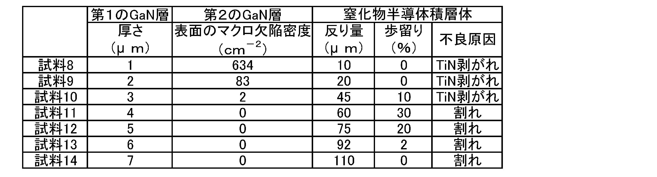
また、試料8~14の各試料にかかる窒化物半導体積層体を形成した。試料8~14ではそれぞれ、AlN層を設けなかったこと以外は、試料1~7と同様に形成した窒化物半導体積層体である。この場合、MOVPE法による一般的な成長方法にならい、AlN層の代わりに、サファイア基板と第1のGaN層4との間に、低温(550℃)の条件下で成長させた、厚さ20nmのGaN層(低温成長GaN層)を形成した。なお、試料8~14の各試料の第1のGaN層の厚さはそれぞれ、下記の表2に示す通りである。
また、試料8~14の各試料にかかる窒化物半導体積層体を形成した。試料8~14ではそれぞれ、AlN層を設けなかったこと以外は、試料1~7と同様に形成した窒化物半導体積層体である。この場合、MOVPE法による一般的な成長方法にならい、AlN層の代わりに、サファイア基板と第1のGaN層4との間に、低温(550℃)の条件下で成長させた、厚さ20nmのGaN層(低温成長GaN層)を形成した。なお、試料8~14の各試料の第1のGaN層の厚さはそれぞれ、下記の表2に示す通りである。
<GaN自立基板の作製>
試料1~試料14の窒化物半導体積層体を下地基板として用い、VAS法によりGaN自立基板を形成した。
試料1~試料14の窒化物半導体積層体を下地基板として用い、VAS法によりGaN自立基板を形成した。
<窒化物半導体積層体の評価>
試料1~14の各試料についてそれぞれ、第2のGaN層の表面のマクロ欠陥密度を測定した。この結果を表1及び表2にそれぞれ示す。
試料1~14の各試料についてそれぞれ、第2のGaN層の表面のマクロ欠陥密度を測定した。この結果を表1及び表2にそれぞれ示す。
試料1~14の各窒化物半導体積層体について、反り量を測定した。この結果を表1及び表2にそれぞれ示す。また、試料1~14の各窒化物半導体積層体について、歩留りを算出した。なお、この歩留りは、各試料である窒化物半導体積層体を下地基板としてGaN自立基板を形成した際の歩留りである。また、歩留りの低下の要因となった、主な不良原因を観察した。これらの結果を表1及び表2にそれぞれ示す。なお、表1及び表2中、「TiN剥がれ」とは、金属膜であるTiN膜が剥がれたことを示す。また、「割れ」とは、窒化物半導体積層体上にGaN自立基板層を形成している際に、窒化物半導体積層体に割れが発生し、GaN自立基板自体に欠陥が生じたことを示している。
<評価結果>
試料1~7の比較から、第1のGaN層の厚さが厚くなるほど、窒化物半導体積層体に生じる反り量が大きくなることを確認した。また、同様のことが試料8~14の比較でも確認できた。
試料1~7の比較から、第1のGaN層の厚さが厚くなるほど、窒化物半導体積層体に生じる反り量が大きくなることを確認した。また、同様のことが試料8~14の比較でも確認できた。
また、試料1~7と試料8~14との比較から、第1のGaN層の厚さが同じ厚さである場合、第1のGaN層に生じる反りの方向と反対方向に反るAlN層を設けた方が、窒化物半導体積層体に生じる反り量を低減することができることを確認した。例えば、試料4と試料11との比較から、HVPE法により厚さが4μmの第1のGaN層を形成した場合、AlN層を設けた試料4の窒化物半導体積層体の反り量は33μmであるのに対し、AlN層を設けなかった試料11の窒化物半導体積層体の反り量は60μmであった。
また、第1のGaN層の厚さを4μm以上と厚くした場合であっても、第1のGaN層に生じる反りの方向とは反対方向に反るAlN層を設けることで、窒化物半導体積層体全体では、反り量を低減することができることを確認した。例えば、窒化物半導体積層体全体では、反り量を60μm未満にすることができることを確認した。
窒化物半導体積層体全体の反り量が低減されることで、歩留りを向上させることができることを確認した。例えば、試料5と試料12との比較から、第1のGaN層の厚さが5μmと同じ厚さである場合、窒化物半導体積層体全体での反り量が小さい試料5の方が、歩留りが高いことを確認した。つまり、窒化物半導体積層体の生産性の低下を抑制することができることを確認した。
また、HVPE法により各層を形成した場合であっても、第1のGaN層の厚さが4μm以上であると、第2のGaN層の表面に現れるマクロ欠陥密度を十分に低下させることができることを確認した。例えば、試料4~7、試料11~14からそれぞれ、第1のGaN層の厚さが4μm以上であると、第2のGaN層の表面のマクロ欠陥密度を0cm-2にすることができることを確認した。
また、試料1~3、試料8~10から、第2のGaN層の表面のマクロ欠陥密度が十分に低減されていない(例えば0cm-2になっていない)と、第2のGaN層上に設けられる金属膜(TiN膜)が第2の基板上から剥がれてしまうことがあることを確認した。その結果、歩留りが10%以下まで低下することがあることを確認した。つまり、窒化物半導体積層体の生産性が低下することがあることを確認した。
<本発明の好ましい態様>
以下に、本発明の好ましい態様について付記する。
以下に、本発明の好ましい態様について付記する。
[付記1]
本発明の一態様によれば、
基板上に窒化アルミニウム層を形成する第1の工程と、
前記窒化アルミニウム層上に第1の窒化ガリウム層を形成する第2の工程と、
前記第1の窒化ガリウム層上に、アルミニウムを含むIII族窒化物半導体層を形成する第3の工程と、
前記III族窒化物半導体層上に、第2の窒化ガリウム層を形成する第4の工程と、
前記第2の窒化ガリウム層上に、金属膜を形成する第5の工程と、
前記第2の窒化ガリウム層及び前記金属膜を多孔質に改質する処理を行う第6の工程と、を有し、
前記第1~第4の各工程をそれぞれ、HVPE法により行う窒化物半導体積層体の製造方法が提供される。
本発明の一態様によれば、
基板上に窒化アルミニウム層を形成する第1の工程と、
前記窒化アルミニウム層上に第1の窒化ガリウム層を形成する第2の工程と、
前記第1の窒化ガリウム層上に、アルミニウムを含むIII族窒化物半導体層を形成する第3の工程と、
前記III族窒化物半導体層上に、第2の窒化ガリウム層を形成する第4の工程と、
前記第2の窒化ガリウム層上に、金属膜を形成する第5の工程と、
前記第2の窒化ガリウム層及び前記金属膜を多孔質に改質する処理を行う第6の工程と、を有し、
前記第1~第4の各工程をそれぞれ、HVPE法により行う窒化物半導体積層体の製造方法が提供される。
[付記2]
付記1の窒化物半導体積層体の製造方法であって、好ましくは、
前記第1の工程では、前記窒化アルミニウム層を形成する温度を800℃以上1200℃以下にする。
付記1の窒化物半導体積層体の製造方法であって、好ましくは、
前記第1の工程では、前記窒化アルミニウム層を形成する温度を800℃以上1200℃以下にする。
[付記3]
付記1又は2の窒化物半導体積層体の製造方法であって、好ましくは、
前記第1の工程では、前記窒化アルミニウム層の厚さを10nm以上500nm以下にする。
付記1又は2の窒化物半導体積層体の製造方法であって、好ましくは、
前記第1の工程では、前記窒化アルミニウム層の厚さを10nm以上500nm以下にする。
[付記4]
付記1ないし3のいずれかの窒化物半導体積層体の製造方法であって、好ましくは、
前記第2の工程では、前記第1の窒化ガリウム層を4μm以上にする。
付記1ないし3のいずれかの窒化物半導体積層体の製造方法であって、好ましくは、
前記第2の工程では、前記第1の窒化ガリウム層を4μm以上にする。
[付記5]
付記1ないし4のいずれかの窒化物半導体積層体の製造方法であって、好ましくは、
前記基板としてサファイア基板を用いる。
付記1ないし4のいずれかの窒化物半導体積層体の製造方法であって、好ましくは、
前記基板としてサファイア基板を用いる。
[付記6]
付記1ないし5のいずれかの窒化物半導体積層体の製造方法であって、好ましくは、
多孔質に改質された前記金属膜上に、自立基板となる窒化ガリウム層を成膜する第7の工程を有する。
付記1ないし5のいずれかの窒化物半導体積層体の製造方法であって、好ましくは、
多孔質に改質された前記金属膜上に、自立基板となる窒化ガリウム層を成膜する第7の工程を有する。
[付記7]
付記6の窒化物半導体積層体の製造方法であって、好ましくは、
前記第7の工程では、前記金属膜から前記自立基板となる窒化ガリウム層を剥離し、前記自立基板を形成する。
付記6の窒化物半導体積層体の製造方法であって、好ましくは、
前記第7の工程では、前記金属膜から前記自立基板となる窒化ガリウム層を剥離し、前記自立基板を形成する。
[付記8]
付記7の窒化物半導体積層体の製造方法であって、好ましくは、
前記第7の工程では、剥離した前記自立基板となる窒化ガリウム層に対してスライス処理を行うことで、1つの前記自立基板となる窒化ガリウム層から複数枚の前記自立基板を形成する。
付記7の窒化物半導体積層体の製造方法であって、好ましくは、
前記第7の工程では、剥離した前記自立基板となる窒化ガリウム層に対してスライス処理を行うことで、1つの前記自立基板となる窒化ガリウム層から複数枚の前記自立基板を形成する。
[付記9]
本発明の他の態様によれば、
基板上に設けられた窒化アルミニウム層と、
前記窒化アルミニウム層上に設けられた第1の窒化ガリウム層と、
前記第1の窒化ガリウム層上に設けられたアルミニウムを含むIII族窒化物半導体層と、
前記III族窒化物半導体層上に設けられ、多孔質な第2の窒化ガリウム層と、
前記第2の窒化ガリウム層上に設けられ、多孔質な金属膜と、を備え、
前記窒化アルミニウム層に生じた反りによって、前記第1の窒化ガリウム層に生じた反りが打ち消されるような力が前記第1の窒化ガリウム層に加えられている窒化物半導体積層体が提供される。
本発明の他の態様によれば、
基板上に設けられた窒化アルミニウム層と、
前記窒化アルミニウム層上に設けられた第1の窒化ガリウム層と、
前記第1の窒化ガリウム層上に設けられたアルミニウムを含むIII族窒化物半導体層と、
前記III族窒化物半導体層上に設けられ、多孔質な第2の窒化ガリウム層と、
前記第2の窒化ガリウム層上に設けられ、多孔質な金属膜と、を備え、
前記窒化アルミニウム層に生じた反りによって、前記第1の窒化ガリウム層に生じた反りが打ち消されるような力が前記第1の窒化ガリウム層に加えられている窒化物半導体積層体が提供される。
[付記10]
付記9の窒化物半導体積層体であって、好ましくは、
前記第1の窒化ガリウム層の厚さが4μm以上である。
付記9の窒化物半導体積層体であって、好ましくは、
前記第1の窒化ガリウム層の厚さが4μm以上である。
[付記11]
付記9又は10の窒化物半導体積層体であって、好ましくは、
前記窒化アルミニウム層の厚さが10nm以上500nm以下である。
付記9又は10の窒化物半導体積層体であって、好ましくは、
前記窒化アルミニウム層の厚さが10nm以上500nm以下である。
[付記12]
付記9ないし11のいずれかの窒化物半導体積層体であって、好ましくは、
前記基板がサファイア基板である。
付記9ないし11のいずれかの窒化物半導体積層体であって、好ましくは、
前記基板がサファイア基板である。
[付記13]
付記9ないし12のいずれかの窒化物半導体積層体であって、好ましくは、
前記金属膜上には、自立基板となる窒化ガリウム層が形成されている。
付記9ないし12のいずれかの窒化物半導体積層体であって、好ましくは、
前記金属膜上には、自立基板となる窒化ガリウム層が形成されている。
1 窒化物半導体積層体
2 基板
3 AlN層
4 第1のGaN層
5 III族窒化物半導体層
6 第2のGaN層
7 金属膜
2 基板
3 AlN層
4 第1のGaN層
5 III族窒化物半導体層
6 第2のGaN層
7 金属膜
Claims (7)
- 基板上に窒化アルミニウム層を形成する第1の工程と、
前記窒化アルミニウム層上に第1の窒化ガリウム層を形成する第2の工程と、
前記第1の窒化ガリウム層上に、アルミニウムを含むIII族窒化物半導体層を形成する第3の工程と、
前記III族窒化物半導体層上に、第2の窒化ガリウム層を形成する第4の工程と、
前記第2の窒化ガリウム層上に、金属膜を形成する第5の工程と、
前記第2の窒化ガリウム層及び前記金属膜を多孔質に改質する処理を行う第6の工程と、を有し、
前記第1~第4の各工程をそれぞれ、HVPE法により行う
窒化物半導体積層体の製造方法。 - 前記第1の工程では、前記窒化アルミニウム層を形成する温度を800℃以上1200℃以下にする
請求項1に記載の窒化物半導体積層体の製造方法。 - 前記第1の工程では、前記窒化アルミニウム層の厚さを10nm以上500nm以下にする
請求項1又は2に記載の窒化物半導体積層体の製造方法。 - 前記第2の工程では、前記第1の窒化ガリウム層を4μm以上にする
請求項1ないし3のいずれかに記載の窒化物半導体積層体の製造方法。 - 基板上に設けられた窒化アルミニウム層と、
前記窒化アルミニウム層上に設けられた第1の窒化ガリウム層と、
前記第1の窒化ガリウム層上に設けられたアルミニウムを含むIII族窒化物半導体層と、
前記III族窒化物半導体層上に設けられ、多孔質な第2の窒化ガリウム層と、
前記第2の窒化ガリウム層上に設けられ、多孔質な金属膜と、を備え、
前記窒化アルミニウム層に生じた反りによって、前記第1の窒化ガリウム層に生じた反りが打ち消されるような力が前記第1の窒化ガリウム層に加えられている
窒化物半導体積層体。 - 前記第1の窒化ガリウム層の厚さが4μm以上である
請求項5に記載の窒化物半導体積層体。 - 前記窒化アルミニウム層の厚さは10nm以上500nm以下である
請求項5又は6に記載の窒化物半導体積層体。
Applications Claiming Priority (2)
| Application Number | Priority Date | Filing Date | Title |
|---|---|---|---|
| JP2015045256A JP2016164108A (ja) | 2015-03-06 | 2015-03-06 | 窒化物半導体積層体の製造方法及び窒化物半導体積層体 |
| JP2015-045256 | 2015-03-06 |
Publications (1)
| Publication Number | Publication Date |
|---|---|
| WO2016143229A1 true WO2016143229A1 (ja) | 2016-09-15 |
Family
ID=56876359
Family Applications (1)
| Application Number | Title | Priority Date | Filing Date |
|---|---|---|---|
| PCT/JP2015/085824 Ceased WO2016143229A1 (ja) | 2015-03-06 | 2015-12-22 | 窒化物半導体積層体の製造方法及び窒化物半導体積層体 |
Country Status (3)
| Country | Link |
|---|---|
| JP (1) | JP2016164108A (ja) |
| TW (1) | TW201704566A (ja) |
| WO (1) | WO2016143229A1 (ja) |
Cited By (1)
| Publication number | Priority date | Publication date | Assignee | Title |
|---|---|---|---|---|
| CN113684539A (zh) * | 2016-12-27 | 2021-11-23 | 住友化学株式会社 | Iii族氮化物层叠体的制造方法、检查方法、以及iii族氮化物层叠体 |
Citations (3)
| Publication number | Priority date | Publication date | Assignee | Title |
|---|---|---|---|---|
| JP2003536257A (ja) * | 2000-06-09 | 2003-12-02 | セントレ・ナショナル・デ・ラ・レシェルシェ・サイエンティフィーク | 窒化ガリウムのコーティングの製造方法 |
| JP2004319711A (ja) * | 2003-04-15 | 2004-11-11 | Hitachi Cable Ltd | エピタキシャル成長用多孔質基板およびその製造方法ならびにiii族窒化物半導体基板の製造方法 |
| JP2014527707A (ja) * | 2011-06-30 | 2014-10-16 | ソイテック | シリコンまたは類似の基板上に窒化ガリウムの厚いエピタキシャル層を形成するための方法、およびこの方法を使用して得られる層 |
-
2015
- 2015-03-06 JP JP2015045256A patent/JP2016164108A/ja active Pending
- 2015-12-22 WO PCT/JP2015/085824 patent/WO2016143229A1/ja not_active Ceased
-
2016
- 2016-01-13 TW TW105100937A patent/TW201704566A/zh unknown
Patent Citations (3)
| Publication number | Priority date | Publication date | Assignee | Title |
|---|---|---|---|---|
| JP2003536257A (ja) * | 2000-06-09 | 2003-12-02 | セントレ・ナショナル・デ・ラ・レシェルシェ・サイエンティフィーク | 窒化ガリウムのコーティングの製造方法 |
| JP2004319711A (ja) * | 2003-04-15 | 2004-11-11 | Hitachi Cable Ltd | エピタキシャル成長用多孔質基板およびその製造方法ならびにiii族窒化物半導体基板の製造方法 |
| JP2014527707A (ja) * | 2011-06-30 | 2014-10-16 | ソイテック | シリコンまたは類似の基板上に窒化ガリウムの厚いエピタキシャル層を形成するための方法、およびこの方法を使用して得られる層 |
Cited By (1)
| Publication number | Priority date | Publication date | Assignee | Title |
|---|---|---|---|---|
| CN113684539A (zh) * | 2016-12-27 | 2021-11-23 | 住友化学株式会社 | Iii族氮化物层叠体的制造方法、检查方法、以及iii族氮化物层叠体 |
Also Published As
| Publication number | Publication date |
|---|---|
| JP2016164108A (ja) | 2016-09-08 |
| TW201704566A (zh) | 2017-02-01 |
Similar Documents
| Publication | Publication Date | Title |
|---|---|---|
| TWI437637B (zh) | 利用自我分裂來製造氮化鎵單晶基板的方法 | |
| TW550312B (en) | Production of low defect, crack-free epitaxial films on a thermally and/or lattice mismatched substrate | |
| JP4117156B2 (ja) | Iii族窒化物半導体基板の製造方法 | |
| KR101321654B1 (ko) | Ⅲ족 질화물 반도체 성장용 기판, ⅲ족 질화물 반도체 에피택셜 기판, ⅲ족 질화물 반도체 소자 및 ⅲ족 질화물 반도체 자립 기판, 및 이들의 제조 방법 | |
| JP4809887B2 (ja) | 窒化ガリウム基板の製造方法 | |
| JP3821232B2 (ja) | エピタキシャル成長用多孔質基板およびその製造方法ならびにiii族窒化物半導体基板の製造方法 | |
| US20160380045A1 (en) | Crystalline semiconductor growth on amorphous and poly-crystalline substrates | |
| US9419160B2 (en) | Nitride semiconductor structure | |
| TW200912054A (en) | Method for preparing substrate for growing gallium nitride and method for preparing gallium nitride substrate | |
| CN107845565A (zh) | 一种提高氮化镓器件电子迁移率及外延层质量方法 | |
| CN101248221B (zh) | 半导体基板制造方法 | |
| JP2014009156A (ja) | 窒化ガリウム基板の製造方法および該方法により製造された窒化ガリウム基板 | |
| JP4130389B2 (ja) | Iii族窒化物系化合物半導体基板の製造方法 | |
| JP4768759B2 (ja) | Iii族窒化物半導体基板 | |
| WO2016143229A1 (ja) | 窒化物半導体積層体の製造方法及び窒化物半導体積層体 | |
| EP2378545A1 (en) | Iii-nitride semiconductor growth substrate, iii-nitride semiconductor epitaxial substrate, iii-nitride semiconductor element, iii-nitride semiconductor freestanding substrate, and method for fabricating these | |
| JP2005518092A (ja) | 適切な基板上における炭化ケイ素又は第iii族元素窒化物の層の製造方法 | |
| JP5430467B2 (ja) | Iii族窒化物半導体成長用基板、iii族窒化物半導体自立基板、iii族窒化物半導体素子、ならびに、これらの製造方法 | |
| JP2013079168A (ja) | 窒化物半導体ウエハの製造方法 | |
| KR101635530B1 (ko) | 다수의 공극을 갖는 질화물 반도체 결정 성장 방법 및 이를 이용한 질화물 반도체 기판 제조 방법 | |
| JP2010225947A (ja) | 窒化物半導体用形成用基板およびその製造方法 | |
| JP5668718B2 (ja) | GaN自立基板の製造方法 | |
| WO2015043961A1 (en) | A semiconductor wafer and a method for producing the semiconductor wafer | |
| JP2013256440A (ja) | 窒化ガリウム基板の製造方法及び該製造方法により製造された窒化ガリウム基板 | |
| WO2012164005A1 (en) | Method and apparatus for fabricating free-standing group iii nitride crystals |
Legal Events
| Date | Code | Title | Description |
|---|---|---|---|
| 121 | Ep: the epo has been informed by wipo that ep was designated in this application |
Ref document number: 15884713 Country of ref document: EP Kind code of ref document: A1 |
|
| NENP | Non-entry into the national phase |
Ref country code: DE |
|
| 122 | Ep: pct application non-entry in european phase |
Ref document number: 15884713 Country of ref document: EP Kind code of ref document: A1 |