WO2016142994A1 - データ収集システム - Google Patents
データ収集システム Download PDFInfo
- Publication number
- WO2016142994A1 WO2016142994A1 PCT/JP2015/056648 JP2015056648W WO2016142994A1 WO 2016142994 A1 WO2016142994 A1 WO 2016142994A1 JP 2015056648 W JP2015056648 W JP 2015056648W WO 2016142994 A1 WO2016142994 A1 WO 2016142994A1
- Authority
- WO
- WIPO (PCT)
- Prior art keywords
- signal
- time
- sensors
- optical signal
- physical quantity
- Prior art date
- Legal status (The legal status is an assumption and is not a legal conclusion. Google has not performed a legal analysis and makes no representation as to the accuracy of the status listed.)
- Ceased
Links
Images

Classifications
-
- G—PHYSICS
- G08—SIGNALLING
- G08C—TRANSMISSION SYSTEMS FOR MEASURED VALUES, CONTROL OR SIMILAR SIGNALS
- G08C17/00—Arrangements for transmitting signals characterised by the use of a wireless electrical link
- G08C17/02—Arrangements for transmitting signals characterised by the use of a wireless electrical link using a radio link
-
- G—PHYSICS
- G08—SIGNALLING
- G08C—TRANSMISSION SYSTEMS FOR MEASURED VALUES, CONTROL OR SIMILAR SIGNALS
- G08C19/00—Electric signal transmission systems
-
- G—PHYSICS
- G08—SIGNALLING
- G08C—TRANSMISSION SYSTEMS FOR MEASURED VALUES, CONTROL OR SIMILAR SIGNALS
- G08C19/00—Electric signal transmission systems
- G08C19/02—Electric signal transmission systems in which the signal transmitted is magnitude of current or voltage
- G08C19/025—Electric signal transmission systems in which the signal transmitted is magnitude of current or voltage using fixed values of magnitude of current or voltage
-
- G—PHYSICS
- G08—SIGNALLING
- G08C—TRANSMISSION SYSTEMS FOR MEASURED VALUES, CONTROL OR SIMILAR SIGNALS
- G08C23/00—Non-electrical signal transmission systems, e.g. optical systems
- G08C23/04—Non-electrical signal transmission systems, e.g. optical systems using light waves, e.g. infrared
Definitions
- the present invention relates to a data collection system that collects measurement data from a plurality of sensors.
- a system for monitoring an object by collecting measurement data obtained by a plurality of detectors arranged at locations apart from each other is known.
- a monitoring device that monitors partial discharge generated in a high-voltage device based on the measurement data change time and the data is disclosed (see Patent Document 1).
- a data collection system that collects measurement data of each sensor at the same time with high accuracy in consideration of transmission delay is disclosed (see Patent Document 2).
- An object of the present invention is to provide a data collection system capable of reducing the setting work for synchronizing a plurality of sensors.
- a data collection system includes a plurality of synchronized sensors and an optical signal distributor, wherein the plurality of sensors includes a physical quantity measuring unit that measures a physical quantity, and the measured physical quantity is predetermined.
- the first optical signal transmitting means for transmitting the first optical signal to the optical signal distributor and the second optical signal received from the optical signal distributor as the second electric signal
- the total time of the first signal conversion means for conversion and the second electric signal converted by the first signal conversion means with the first conversion time by the first signal conversion means is the plurality of times.
- a first delay time set to be all the same by the sensor, a first delay means for delaying, and when the physical quantity satisfies the condition, the physical quantity measured at the time when the condition is satisfied is transmitted.
- the optical signal distributor includes a plurality of second signal conversion means for converting the first optical signal output from each of the plurality of sensors into a first electric signal, and the plurality of second signal conversions. Second delay times respectively set so that the total time of the first electric signals converted by the respective means and the respective conversion times by the plurality of second signal conversion means are all the same.
- a plurality of second delay means for delaying and each of the plurality of sensors when receiving the first electrical signal delayed from at least one of the plurality of second delay means
- a second optical signal transmitting means for transmitting the second optical signal to said first signal converting means.
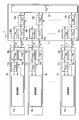
- FIG. 1 is a configuration diagram showing the configuration of the data collection system according to the first embodiment of the present invention.
- FIG. 2 is a configuration diagram illustrating the transmission time of the trigger signal in the data collection system according to the present embodiment.
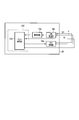
- FIG. 3 is a configuration diagram showing a configuration of a sensor according to the second embodiment of the present invention.
- FIG. 1 is a configuration diagram showing a configuration of a data collection system 1 according to the first embodiment of the present invention.
- symbol is attached
- the data collection system 1 includes n sensors 2a, 2b,..., 2n, an optical signal distributor 3, a plurality of optical transmission lines 4, and a data collection device 5. Any number of sensors 2a to 2n may be provided as long as it is two or more.
- the sensors 2a to 2n and the optical signal distributor 3 are connected by two optical transmission lines 4 for transmission and reception, respectively.
- the optical transmission line 4 is, for example, an optical fiber.
- the data collection device 5 may not be provided as a configuration of the data collection system 1. Since the data collection device 5 is only required to receive the measurement data DT from the sensors 2a to 2n, the data collection device 5 may be installed anywhere.
- Sensors 2a to 2n are arranged at measurement points such as an electronic device or its periphery.
- the sensors 2a to 2n measure a physical quantity by sampling a change in a physical quantity such as voltage, current, or electromagnetic wave in nanosecond order.
- the sensors 2a to 2n transmit the measured physical quantity measurement data DT to the data collection device 5 that collects the measurement data DT by wireless communication.
- the sensors 2a to 2n transmit the measurement data DT by two triggers, an internal trigger generated by a change in physical quantity measured by itself and an external trigger generated by a change in physical quantity measured by the other sensors 2a to 2n.
- the sensors 2a to 2n are all configured in the same manner except that the measurement target (measurement location or physical quantity to be measured) is different.
- the measurement target measurement location or physical quantity to be measured
- one sensor 2a will be described, and the remaining sensors 2b to 2n are assumed to be configured in the same manner, and description thereof will be omitted.
- the sensor 2a includes an analog signal input unit 11a, an analog / digital conversion unit 12a, an arithmetic processing unit 13a, a data storage unit 14a, a data editing unit 15a, a radio communication circuit 16a, a delay circuit 17a, an O / E converter 18a, and an E / E converter.
- An O converter 19a and a radio communication antenna 20a are provided.
- the sensor 2a has a configuration necessary for synchronizing the reference vibrator and the like.
- the analog signal input unit 11a receives an analog signal (electric signal) representing a physical quantity that is a measurement target of the sensor 2a.
- the analog signal input unit 11a converts the input analog signal into an analog signal for handling as a measurement value (measurement data) and outputs the analog signal to the analog / digital conversion unit 12a.
- the analog / digital converter 12a converts the measured value of the analog signal input from the analog signal input unit 11a into a digital signal.
- the analog / digital conversion unit 12a outputs the measured value of the converted digital signal to the arithmetic processing unit 13a and the data storage unit 14a.
- the arithmetic processing unit 13a is configured by an element such as a central processing unit (CPU) being executed according to a program or the like.
- the arithmetic processing unit 13a samples the measurement value (digital signal) output from the analog / digital conversion unit 12a in nanosecond order.
- the arithmetic processing unit 13a writes the sampled measurement value to the data storage unit 14a.
- the arithmetic processing unit 13a performs monitoring and control of components or elements in the sensor 2a.
- the data storage unit 14a is a memory that stores the sampled measurement values in time series.
- the data storage unit 14a has a sufficiently large capacity so as to correspond to the function of the sensor 2a.
- the data storage unit 14a stores data in a ring buffer format, for example.
- the arithmetic processing unit 13a includes a comparison unit 131 and a determination unit 132.
- the comparison unit 131 receives the measurement values sampled from the analog / digital conversion unit 12a.
- the comparison unit 131 compares the sampled measurement value with a predetermined threshold value (set value).
- a predetermined threshold value set value
- the comparison unit 131 transmits an internal trigger signal to the determination unit 132 and the E / O converter 19a.
- the internal trigger signal is transmitted when the measured value exceeds the threshold.
- Condition may be sufficient.
- the condition for transmitting the internal trigger signal may be when the measured value falls below the set value, or when the change amount of the measured value exceeds the set value.
- the determination unit 132 receives the internal trigger signal output from the comparison unit 131 and the external trigger signal output from the other sensors 2b to 2n. When both the internal trigger signal and the external trigger signal are received, the determination unit 132 determines that the measured value of the own sensor 2a exceeds the threshold (detection by the own sensor 2a). When receiving the external trigger signal and not receiving the internal trigger signal, the determination unit 132 determines that the measurement values of the other sensors 2b to 2n have exceeded the threshold (detection by the other sensors 2b to 2n). The determination unit 132 outputs, together with the determination result, a trigger signal that instructs data editing and data transmission to the data editing unit 15a.
- the data editing unit 15a When receiving the determination result and the trigger signal from the determination unit 132, the data editing unit 15a takes in the measurement data from the data storage unit 14a based on the determination result.
- the data editing unit 15a takes in the measurement data measured at the generation time of the internal trigger signal from the data storage unit 14a.
- the data editing unit 15a measures the measurement data measured at a time that goes back a predetermined time before the reception time of the external trigger signal. From the data storage unit 14a.
- the data editing unit 15a adds information necessary for wireless transmission such as a header and a footer to the measurement data captured from the data storage unit 14a to generate a wireless transmission packet.
- the measurement data included in the packet by the data editing unit 15a may be any measurement data as long as it is obtained from the data stored in the data storage unit 14a.
- the measurement data included in the packet may be an instantaneous value or an effective value at the corresponding time, or may be waveform data obtained by editing the measurement values before and after the corresponding time.
- the data editing unit 15a outputs the generated packet to the wireless communication circuit 16a.
- the wireless communication circuit 16a outputs a packet including the measurement data DT received from the data editing unit 15a from the wireless communication antenna 20a. Thereby, the measurement data DT of the sensor 2a is transmitted to the external data collection device 5 by wireless communication.
- the O / E converter 18a receives an external trigger signal (optical signal) generated by the detection of the other sensors 2b to 2n from the optical signal distributor 3 via the optical transmission line 4.
- the O / E converter 18a converts the received external trigger signal from an optical signal to an electrical signal.
- the O / E converter 18a outputs an external trigger signal converted into an electric signal to the delay circuit 17a.
- the delay circuit 17a delays the external trigger signal input from the O / E converter 18a by a preset delay time and outputs the signal to the determination unit 132.
- the delay time set in the delay circuit 17a is determined according to the time (conversion time) required for the conversion by the O / E converter 18a.
- the E / O converter 19a converts the internal trigger signal input from the comparison unit 131 from an electric signal to an optical signal.
- the E / O converter 19 a outputs the internal trigger signal converted into the optical signal to the optical signal distributor 3 through the optical transmission path 4.
- the internal trigger signal output from the E / O converter 19a is a signal that is treated as an external trigger signal by the other sensors 2b to 2n.
- the optical signal distributor 3 When receiving the internal trigger signal of the optical signal output from any of the sensors 2a to 2n, the optical signal distributor 3 distributes the optical signal as the external trigger signal to all the other sensors 2a to 2n.
- the optical signal distributor 3 includes n O / E converters 31a to 31n, n delay circuits 32a to 32n, an OR circuit 33, and n E / O converters 34a to 34n.
- the same number of O / E converters 31a to 31n, delay circuits 32a to 32n, and E / O converters 34a to 34n are provided so as to correspond to the respective sensors 2a to 2n.
- the O / E converter 31a, the delay circuit 32a, and the E / O converter 34a corresponding to one sensor 2a will be mainly described, and the rest will be omitted because they are configured in the same manner.
- the O / E converter 31a receives the trigger signal (internal trigger signal) of the optical signal transmitted from the sensor 2a.
- the O / E converter 31a converts the received trigger signal from an optical signal to an electrical signal.
- the O / E converter 31a outputs the trigger signal converted into an electric signal to the delay circuit 32a.
- the delay circuit 32a delays the trigger signal input from the O / E converter 31a by a preset delay time and outputs the delayed signal to the OR circuit 33.
- the delay time set in the delay circuit 32a is determined according to the time (conversion time) required for the conversion by the O / E converter 31a.
- Trigger signals from all delay circuits 32a to 32n corresponding to all sensors 2a to 2n are input to the OR circuit 33.
- the OR circuit 33 calculates the logical sum of the trigger signals from all the delay circuits 32a to 32n and outputs the calculation result to the E / O converters 34a to 34n corresponding to all the sensors 2a to 2n. Accordingly, when receiving the trigger signal from at least one delay circuit 32a to 32n, the logical sum circuit 33 outputs the trigger signal to all the E / O converters 34a to 34n.
- the E / O converter 34a receives the trigger signal of the electric signal from the OR circuit 33.
- the E / O converter 34a converts the received trigger signal from an electric signal to an optical signal.
- the E / O converter 34a transmits the trigger signal converted into the optical signal to the sensor 2a through the optical transmission line 4 as an external trigger signal.
- FIG. 2 is a configuration diagram showing the transmission time of the trigger signal in the data collection system 1 according to the present embodiment.
- a method for determining the delay times T17a to T17n set in the delay circuits 17a to 17n of the sensors 2a to 2n and the delay times T32a to T32n set to the delay circuits 32a to 32n of the optical signal distributor 3 will be described.
- the conversion times T18a to T18n and T31a to T31n for converting the optical signals of the O / E converters 18a to 18n and 31a to 31n into electric signals are all different due to individual differences. For example, there is a difference of about 100 nanoseconds in the conversion times T18a to T18n and T31a to T31n between individuals.
- the conversion times for converting the electrical signals from the electrical signals of the E / O converters 19a to 19n and 34a to 34n into optical signals can be regarded as zero.
- the delay time T17a is such that the sum of the delay times T17a to T17n of the delay circuits 17a to 17n and the conversion times T18a to T18n of the O / E converters 18a to 18n are all the same time Ta.
- To T17n are set.
- the time Ta is set to a value larger than the individual difference between the conversion times T18a to T18n of the O / E converters 18a to 18n.
- the time Ta is a delay time required for transmission from the external trigger signal received by the O / E converters 18a to 18n until reaching the arithmetic processing units 13a to 13n in each of the sensors 2a to 2n.
- the delay time T32a is set such that the sum of the delay times T32a to T32n of the delay circuits 32a to 32n and the conversion times T31a to T31n of the O / E converters 31a to 31n all become the same time Tb.
- To T32n are set.
- the time Tb is set to a value larger than the individual difference between the conversion times T31a to T31n of the O / E converters 31a to 31n.
- the time Tb is a delay time required for transmission from when the internal trigger signals of the sensors 2a to 2n are received by the O / E converters 31a to 31n of the optical signal distributor 3 until reaching the OR circuit 33. .
- the delay time Td until the internal trigger signal generated by the sensor 2b is transmitted to the sensor 2a as an external trigger signal will be described.
- the delay time Td is expressed as follows.
- Td T19b + T4 + T31b + T32b + T33 + T34a + T4 + T18a + T17a (1)
- the time T4 is the time taken for the optical signal to travel through the optical transmission line 4 (signal transmission time)
- the time T33 is the arithmetic processing time of the OR circuit 33
- the time T19b is the E / O converter 19b.
- the signal conversion time, T34a is the signal conversion time of the E / O converter 34a.
- Td T19b + T4 + Tb + T33 + T34a + T4 + Ta (4)
- the equation (4) becomes as follows.
- Td T4 + Tb + T33 + T4 + Ta (5)
- the arithmetic processing time T33 of the OR circuit 33 is fixed.
- the signal transmission time T4 of the optical transmission line 4 is determined by the length of the cable and is fixed.
- the delay time Td becomes a fixed time.
- the delay time Td is obtained as follows.
- the delay time T32b of the delay circuit 32b and the delay time T17a of the delay circuit 17a are obtained by the following equations from the equations (2) and (3).
- the delay times T17a and T32b are obtained by determining the time Ta and the time Tb and measuring the conversion times T19b and T34a of the E / O converters 19b and 34a.
- the obtained delay times T17a and T32b are set in the delay circuits 17a and 32b before operation. This is performed for all the delay circuits 17a to 17n and 32a to 32n.
- the plurality of sensors 2a to 2n can be synchronized with high accuracy.
- the data collection system 1 can collect measurement values determined at the same time with high accuracy from the plurality of sensors 2a to 2n.
- the delay circuits 17a to 17n and 32a to 32n are configured with delay elements that can be set in units of 0.1 nanoseconds
- the delay times T17a to T17n and T32a to T32n may be set in units of 0.1 nanoseconds. it can.
- the accuracy of synchronization of the measurement time between the plurality of sensors 2a to 2n can be set to 0.1 nanosecond unit.
- delay circuits 17a to 17n and 32a to 32n are provided in the individual sensors 2a to 2n and the optical signal distributor 3, respectively. Thereby, even when the combination of the sensors 2a to 2n and the optical signal distributor 3 is arbitrarily selected, the setting work of the delay times T17a to T17n and T32a to T32n can be reduced. For example, when any one of the sensors 2a to 2n or the optical signal distributor 3 needs to be replaced, delay circuits 17a to 17n provided in the replaced apparatus (the sensors 2a to 2n or the optical signal distributor 3), If only 32a to 32n are set again, the setting operation for synchronization in the data collection system 1 can be completed.
- FIG. 3 is a configuration diagram showing the configuration of the sensor 2A according to the second embodiment of the present invention.
- the data collection system 1 according to this embodiment is obtained by replacing the sensors 2a to 2n with the sensors 2A in the data collection system 1 according to the first embodiment shown in FIG. Others are the same as in the first embodiment.
- the sensor 2A is a sensor 2a according to the first embodiment shown in FIG. 1, in which an arithmetic processing unit 13A is provided instead of the arithmetic processing unit 13a. Otherwise, the sensor 2A is the same as the sensor 2a according to the first embodiment.
- the arithmetic processing unit 13A is obtained by adding a test execution unit 133 to the arithmetic processing unit 13a according to the first embodiment. Otherwise, the arithmetic processing unit 13A is the same as the arithmetic processing unit 13a according to the first embodiment. In FIG. 3, only the test execution unit 133 is shown for convenience of explanation.
- the test execution unit 133 performs arithmetic processing for executing the test mode (signal delay time measurement function).
- the test execution unit 133 measures the signal delay time Tt from when the test signal is output until it is received by the test execution unit 133 via the optical transmission line 4.
- the test execution unit 133 performs arithmetic processing for performing a test. Note that switching between the normal mode and the test mode executed in the operation state may be performed in any manner. For example, the mode switching may be performed by either software or hardware, may be artificially switched, or may be performed by automatically recognizing the operation state or the test state.
- the test is performed in a single state in which the sensor 2A is separated from the data collection system 1. Note that the test may be performed without being disconnected from the data collection system 1.
- the worker connects the terminal from which the internal trigger signal is output and the terminal from which the external trigger signal is input through the optical transmission line 4 so that the trigger signal output from the sensor 2A is received by the worker.
- the output side of the E / O converter 19a and the input side of the O / E converter 18a are connected by the optical transmission line 4.
- test execution unit 133 The operator operates the sensor 2A to execute a test after connecting the optical transmission line 4. Accordingly, a test signal that is a trigger signal for testing is transmitted from the test execution unit 133.
- the test signal output from the test execution unit 133 is converted from an electrical signal to an optical signal by the E / O converter 19a.
- the test signal converted into the optical signal is output from the E / O converter 19a to the optical transmission line 4.
- the O / E converter 18 a receives the test signal via the optical transmission line 4.
- the O / E converter 18a converts the received test signal from an optical signal to an electrical signal and outputs the signal to the delay circuit 17a.
- the delay circuit 17a delays a preset delay time T17a after receiving the test signal, and outputs it to the test execution unit 133.
- the delay time T17a is set to 0 seconds. Therefore, when receiving the test signal, the delay circuit 17a transmits the test signal without delay.
- the test execution unit 133 measures the time from when the test signal is transmitted until it is received.
- the signal delay time Tt in this case is expressed as the following equation.
- Tt T19a + T4 + T18a + T17a (8)
- the conversion time T19a of the E / O converter 19a and the delay time T17a of the delay circuit 17a are both set to 0 seconds.
- equation (8) becomes as follows.
- Tt T4 + T18a (9) Further, by obtaining the length of the optical transmission line 4, the signal transmission time T4 of the optical transmission line 4 is obtained. Therefore, if the signal delay time Tt is measured, the conversion time T18a of the O / E converter 18a can be obtained.
- the operator Based on the obtained conversion time T18a of the O / E converter 18a, the operator makes the total time of the delay time T17a of the delay circuit 17a and the conversion time T18a of the O / E converter 18a become a predetermined time Ta.
- the delay time T17a is set in the delay circuit 17a.
- the time Ta is a time for making the total time of the delay time T17a of the delay circuit 17a and the conversion time T18a of the O / E converter 18a the same in all the sensors 2A.
- the time Ta and the signal transmission time T4 of the optical transmission line 4 are set in the sensor 2A in advance in the sensor 2A so that the delay time T17a is automatically set in the delay circuit 17a after the test is completed. May be.
- the delay of the delay circuit 17a of the sensor 2A Time T17a can be easily set.
- the present invention is not limited to the above-described embodiment as it is, and can be embodied by modifying constituent elements without departing from the scope of the invention in the implementation stage.
- various inventions can be formed by appropriately combining a plurality of components disclosed in the embodiment. For example, some components may be deleted from all the components shown in the embodiment.
- constituent elements over different embodiments may be appropriately combined.
Landscapes
- Physics & Mathematics (AREA)
- General Physics & Mathematics (AREA)
- Engineering & Computer Science (AREA)
- Computer Networks & Wireless Communication (AREA)
- Arrangements For Transmission Of Measured Signals (AREA)
Abstract
Description
図1は、本発明の第1の実施形態に係るデータ収集システム1の構成を示す構成図である。なお、図面における同一部分には同一符号を付して、重複する説明を省略する。
ここで、時間T4は、光信号が光伝送路4を伝達するのに掛かる時間(信号伝達時間)、時間T33は、論理和回路33の演算処理時間、時間T19bは、E/O変換器19bの信号の変換時間、時間T34aは、E/O変換器34aの信号の変換時間、である。
Tb=T31a+T32a=T31b+T32b=…=T31n+T32n …式(3)
式(2)及び式(3)を式(1)に代入すると、次式になる。
ここで、E/O変換器19b,34aの変換時間T19b,T34aは0とみなせるため、式(4)は、次式のようになる。
ここで、論理和回路33の演算処理時間T33は、固定である。また、光伝送路4の信号伝達時間T4は、ケーブルの長さで決まり、固定である。
従って、この条件下では、センサー2bで発生したトリガー信号をセンサー2aが受信した場合、センサー2aは、トリガー信号を受信した時刻から375ナノ秒前の測定値をとれば、トリガー信号を発生した時刻のセンサー2bの測定値と同期する。
T19a=Ta-T18a=200-60=140[ns] …式(7)
このように、時間Ta及び時間Tbを決め、E/O変換器19b,34aの変換時間T19b,T34aを測定することで、遅延時間T17a,T32bが求まる。求めた遅延時間T17a,T32bを遅延回路17a,32bに運用前に設定する。これを全ての遅延回路17a~17n,32a~32nに対して行う。
図3は、本発明の第2の実施形態に係るセンサー2Aの構成を示す構成図である。
ここでは、E/O変換器19aの変換時間T19a及び遅延回路17aの遅延時間T17aは、共に0秒に設定されている。
また、光伝送路4の長さを求めることにより、光伝送路4の信号伝達時間T4が求まる。従って、信号遅延時間Ttを測定すれば、O/E変換器18aの変換時間T18aが求まる。
Claims (6)
- 同期される複数のセンサーと、
光信号分配器とを備え、
前記複数のセンサーは、
物理量を測定する物理量測定手段と、
測定した前記物理量が予め決められた条件を満たすと、第1の光信号を前記光信号分配器に送信する第1の光信号送信手段と、
前記光信号分配器から受信する第2の光信号を第2の電気信号に変換する第1の信号変換手段と、
前記第1の信号変換手段により変換された前記第2の電気信号を、前記第1の信号変換手段による第1の変換時間との合計時間が前記複数のセンサーで全て同じになるように設定される第1の遅延時間、遅延させる第1の遅延手段と、
前記物理量が前記条件を満したとき、前記条件を満した時刻に測定された前記物理量を送信し、前記第1の遅延手段により遅延された前記第2の電気信号を受信したとき、前記第2の電気信号を受信した時刻から予め決められた時間前に測定された前記物理量を送信するデータ送信手段とをそれぞれ備え、
前記光信号分配器は、
前記複数のセンサーのそれぞれから出力される前記第1の光信号を第1の電気信号にそれぞれ変換する複数の第2の信号変換手段と、
前記複数の第2の信号変換手段によりそれぞれ変換された前記第1の電気信号を、前記複数の第2の信号変換手段によるそれぞれの変換時間との合計時間が全て同じになるようにそれぞれ設定される第2の遅延時間、それぞれ遅延させる複数の第2の遅延手段と、
前記複数の第2の遅延手段のうち少なくとも1つから遅延された前記第1の電気信号を受信したとき、前記複数のセンサーのそれぞれの前記第1の信号変換手段に前記第2の光信号を送信する第2の光信号送信手段とを備えること
を特徴とするデータ収集システム。 - 前記データ送信手段は、無線で送信すること
を特徴とする請求項1に記載のデータ収集システム。 - 前記データ送信手段は、測定された前記物理量を編集して、送信すること
を特徴とする請求項1に記載のデータ収集システム。 - 前記複数のセンサーは、
テスト信号を出力するテスト信号出力手段と、
前記テスト信号出力手段により前記テスト信号が出力されてから、前記第1の光信号送信手段により送信され、前記第1の信号変換手段により電気信号に変換されて受信するまでの時間を計測する時間計測手段とを備えること
を特徴とする請求項1に記載のデータ収集システム。 - 前記複数のセンサーにより測定された物理量を受信するデータ収集装置
を備えることを特徴とする請求項1に記載のデータ収集システム。 - 同期される複数のセンサー及び光信号分配器を用いるデータ収集方法であって、
前記複数のセンサーは、
物理量を測定し、
測定した前記物理量が予め決められた条件を満たすと、第1の光信号を前記光信号分配器に送信し、
前記光信号分配器から受信する第2の光信号を第2の電気信号に変換し、
変換された前記第2の電気信号を、前記第2の電気信号に変換する変換時間との合計時間が前記複数のセンサーで全て同じになるように設定される第1の遅延時間、遅延させ、
前記物理量が前記条件を満したとき、前記条件を満した時刻に測定された前記物理量を送信し、遅延された前記第2の電気信号を受信したとき、前記第2の電気信号を受信した時刻から予め決められた時間前に測定された前記物理量を送信することをそれぞれ含み、
前記光信号分配器は、
前記複数のセンサーのそれぞれから出力される前記第1の光信号を第1の電気信号にそれぞれ変換し、
変換された前記第1の電気信号を、それぞれの前記第1の電気信号に変換する変換時間との合計時間が全て同じになるようにそれぞれ設定される第2の遅延時間、それぞれ遅延させ、
少なくとも1つから遅延された前記第1の電気信号を受信したとき、前記複数のセンサーのそれぞれに前記第2の光信号を送信することを含むこと
を特徴とするデータ収集方法。
Priority Applications (6)
| Application Number | Priority Date | Filing Date | Title |
|---|---|---|---|
| CN201580077486.1A CN107408333B (zh) | 2015-03-06 | 2015-03-06 | 数据收集系统 |
| JP2017504319A JP6274351B2 (ja) | 2015-03-06 | 2015-03-06 | データ収集システム |
| PCT/JP2015/056648 WO2016142994A1 (ja) | 2015-03-06 | 2015-03-06 | データ収集システム |
| KR1020177023857A KR101963524B1 (ko) | 2015-03-06 | 2015-03-06 | 데이터 수집 시스템 |
| TW104113493A TWI575482B (zh) | 2015-03-06 | 2015-04-28 | 資料收集系統 |
| US15/696,764 US11113955B2 (en) | 2015-03-06 | 2017-09-06 | Data collection system |
Applications Claiming Priority (1)
| Application Number | Priority Date | Filing Date | Title |
|---|---|---|---|
| PCT/JP2015/056648 WO2016142994A1 (ja) | 2015-03-06 | 2015-03-06 | データ収集システム |
Related Child Applications (1)
| Application Number | Title | Priority Date | Filing Date |
|---|---|---|---|
| US15/696,764 Continuation US11113955B2 (en) | 2015-03-06 | 2017-09-06 | Data collection system |
Publications (1)
| Publication Number | Publication Date |
|---|---|
| WO2016142994A1 true WO2016142994A1 (ja) | 2016-09-15 |
Family
ID=56878604
Family Applications (1)
| Application Number | Title | Priority Date | Filing Date |
|---|---|---|---|
| PCT/JP2015/056648 Ceased WO2016142994A1 (ja) | 2015-03-06 | 2015-03-06 | データ収集システム |
Country Status (6)
| Country | Link |
|---|---|
| US (1) | US11113955B2 (ja) |
| JP (1) | JP6274351B2 (ja) |
| KR (1) | KR101963524B1 (ja) |
| CN (1) | CN107408333B (ja) |
| TW (1) | TWI575482B (ja) |
| WO (1) | WO2016142994A1 (ja) |
Families Citing this family (3)
| Publication number | Priority date | Publication date | Assignee | Title |
|---|---|---|---|---|
| US10969760B2 (en) * | 2018-04-12 | 2021-04-06 | Faro Technologies, Inc. | Coordinate measurement system with auxiliary axis |
| US11874101B2 (en) | 2018-04-12 | 2024-01-16 | Faro Technologies, Inc | Modular servo cartridges for precision metrology |
| WO2020202473A1 (ja) * | 2019-04-02 | 2020-10-08 | 三菱電機株式会社 | 駆動制御装置 |
Citations (3)
| Publication number | Priority date | Publication date | Assignee | Title |
|---|---|---|---|---|
| JP2002131366A (ja) * | 2000-10-20 | 2002-05-09 | Toshiba Corp | 高電圧機器の内部部分放電監視装置 |
| JP2008295298A (ja) * | 2001-02-09 | 2008-12-04 | Toshiba Corp | 変電機器保護制御システム |
| JP2010218056A (ja) * | 2009-03-13 | 2010-09-30 | Toshiba Mitsubishi-Electric Industrial System Corp | データ収集システム |
Family Cites Families (21)
| Publication number | Priority date | Publication date | Assignee | Title |
|---|---|---|---|---|
| US5105292A (en) * | 1989-10-02 | 1992-04-14 | Alcatel Cit | Asynchronous optical communication system |
| US6091525A (en) * | 1997-11-26 | 2000-07-18 | Lucent Technologies Inc. | Spectral monitoring device and method using data correlation for WDM systems |
| KR20000046903A (ko) * | 1998-12-31 | 2000-07-25 | 이종수 | 범용 측위 시스템을 이용한 다단자 송전선로의 송수신장치 및방법 |
| JP2000249746A (ja) * | 1999-02-26 | 2000-09-14 | Ando Electric Co Ltd | 集積回路試験装置 |
| DE10028144C1 (de) * | 2000-06-07 | 2001-11-29 | Siemens Ag | Messverfahren zur Bestimmung der Nichtlinearitäten einer optischen Faser |
| JP4147730B2 (ja) * | 2000-07-12 | 2008-09-10 | 沖電気工業株式会社 | 波長多重伝送システム |
| JP4046462B2 (ja) * | 2000-07-12 | 2008-02-13 | 沖電気工業株式会社 | 波長多重伝送システム |
| US20030072051A1 (en) * | 2000-10-16 | 2003-04-17 | Myers Michael H. | Orthogonal-code, photonic multiplexing |
| US20020044316A1 (en) * | 2000-10-16 | 2002-04-18 | Myers Michael H. | Signal power allocation apparatus and method |
| JP3907998B2 (ja) | 2001-02-09 | 2007-04-18 | 株式会社東芝 | 変電機器保護制御システム |
| US7068948B2 (en) * | 2001-06-13 | 2006-06-27 | Gazillion Bits, Inc. | Generation of optical signals with return-to-zero format |
| JP2003075261A (ja) * | 2001-08-16 | 2003-03-12 | Agilent Technol Inc | 光パルス測定装置 |
| US6946827B2 (en) * | 2001-11-13 | 2005-09-20 | Nxtphase T & D Corporation | Optical electric field or voltage sensing system |
| KR100699510B1 (ko) * | 2005-08-31 | 2007-03-23 | 강릉대학교산학협력단 | 무선 센서 네트워크를 위한 정확한 시간 동기화 프로토콜 |
| WO2008044193A2 (en) * | 2006-10-12 | 2008-04-17 | Philips Intellectual Property & Standards Gmbh | Method and system for time synchronization in a sensor network |
| KR101509243B1 (ko) * | 2007-07-12 | 2015-04-08 | 한국전자통신연구원 | 무선 센서 네트워크에서 시간 동기화 방법 및 예약 기법을이용한 저전력 라우팅 방법, 그리고 이를 수행하기 위한장치 |
| US9166705B2 (en) * | 2008-06-05 | 2015-10-20 | Samsung Electronics Co., Ltd. | Semiconductor apparatuses having optical connections between memory controller and memory module |
| CN101883014B (zh) * | 2010-07-22 | 2014-03-12 | 中兴通讯股份有限公司 | 一种性能统计数据的采集方法和系统 |
| WO2013037850A1 (de) * | 2011-09-12 | 2013-03-21 | Continental Teves Ag & Co. Ohg | Zeitkorrigiertes sensorsystem |
| CN102508297B (zh) * | 2011-10-08 | 2013-06-26 | 天津大学 | 多节点同步采集时间误差的精确测量和校正方法及装置 |
| JP5978933B2 (ja) * | 2012-11-09 | 2016-08-24 | オムロン株式会社 | センサシステム |
-
2015
- 2015-03-06 KR KR1020177023857A patent/KR101963524B1/ko active Active
- 2015-03-06 WO PCT/JP2015/056648 patent/WO2016142994A1/ja not_active Ceased
- 2015-03-06 JP JP2017504319A patent/JP6274351B2/ja active Active
- 2015-03-06 CN CN201580077486.1A patent/CN107408333B/zh active Active
- 2015-04-28 TW TW104113493A patent/TWI575482B/zh active
-
2017
- 2017-09-06 US US15/696,764 patent/US11113955B2/en active Active
Patent Citations (3)
| Publication number | Priority date | Publication date | Assignee | Title |
|---|---|---|---|---|
| JP2002131366A (ja) * | 2000-10-20 | 2002-05-09 | Toshiba Corp | 高電圧機器の内部部分放電監視装置 |
| JP2008295298A (ja) * | 2001-02-09 | 2008-12-04 | Toshiba Corp | 変電機器保護制御システム |
| JP2010218056A (ja) * | 2009-03-13 | 2010-09-30 | Toshiba Mitsubishi-Electric Industrial System Corp | データ収集システム |
Also Published As
| Publication number | Publication date |
|---|---|
| US11113955B2 (en) | 2021-09-07 |
| TW201633266A (zh) | 2016-09-16 |
| CN107408333B (zh) | 2019-12-31 |
| TWI575482B (zh) | 2017-03-21 |
| US20170365164A1 (en) | 2017-12-21 |
| JPWO2016142994A1 (ja) | 2017-06-22 |
| CN107408333A (zh) | 2017-11-28 |
| JP6274351B2 (ja) | 2018-02-07 |
| KR101963524B1 (ko) | 2019-03-28 |
| KR20170108098A (ko) | 2017-09-26 |
Similar Documents
| Publication | Publication Date | Title |
|---|---|---|
| JP5399592B1 (ja) | 電力系統の情報を収集するマージングユニット | |
| US9970974B2 (en) | On-line status diagnosis device and on-line status diagnosis method for electric power utilities | |
| US8798220B2 (en) | Signal source synchronization circuit | |
| JP6274351B2 (ja) | データ収集システム | |
| US7411533B2 (en) | ADC for simultaneous multiple analog inputs | |
| JP5507025B1 (ja) | 電流差動リレー | |
| CN111044085B (zh) | 安全电路和用于测试在自动化设备中的安全电路的方法 | |
| JP6548592B2 (ja) | 保護制御装置 | |
| JP6501993B1 (ja) | プロセスバス適用保護システムおよびインテリジェント電子デバイス | |
| JP4996992B2 (ja) | インピーダンス測定装置 | |
| JP2011196882A (ja) | レーダ搬送波監視装置 | |
| KR101777038B1 (ko) | 보호 릴레이 장치 | |
| JP2015133544A (ja) | 電力計測装置および保護制御システム | |
| JP6304000B2 (ja) | マージングユニット | |
| KR20130045597A (ko) | 다채널 디지털 수신 방법 및 장치 | |
| CN121431957A (zh) | 测量gis设备回路电阻的方法和装置 | |
| JP2016057237A (ja) | マージングユニット、トリガ信号出力方法、及びマージングユニットテストシステム | |
| JP2004157840A (ja) | 信号変換装置 | |
| JP2012058205A (ja) | 設置環境調査装置、及び設置環境調査システム | |
| CN105656565A (zh) | 矢量驻波检测方法、装置及基站 | |
| WO2020044518A1 (ja) | 同期システム、測定同期システム、同期方法、プログラム | |
| JP2005176411A (ja) | 保護制御装置 | |
| KR20140111826A (ko) | 아날로그 출력모듈의 오프셋 게인 설정방법 | |
| JP2013153238A (ja) | Ifm受信機 |
Legal Events
| Date | Code | Title | Description |
|---|---|---|---|
| 121 | Ep: the epo has been informed by wipo that ep was designated in this application |
Ref document number: 15884492 Country of ref document: EP Kind code of ref document: A1 |
|
| ENP | Entry into the national phase |
Ref document number: 2017504319 Country of ref document: JP Kind code of ref document: A |
|
| ENP | Entry into the national phase |
Ref document number: 20177023857 Country of ref document: KR Kind code of ref document: A |
|
| NENP | Non-entry into the national phase |
Ref country code: DE |
|
| 122 | Ep: pct application non-entry in european phase |
Ref document number: 15884492 Country of ref document: EP Kind code of ref document: A1 |