WO2016136852A1 - 信号発生回路、電圧変換装置及び信号発生方法 - Google Patents
信号発生回路、電圧変換装置及び信号発生方法 Download PDFInfo
- Publication number
- WO2016136852A1 WO2016136852A1 PCT/JP2016/055543 JP2016055543W WO2016136852A1 WO 2016136852 A1 WO2016136852 A1 WO 2016136852A1 JP 2016055543 W JP2016055543 W JP 2016055543W WO 2016136852 A1 WO2016136852 A1 WO 2016136852A1
- Authority
- WO
- WIPO (PCT)
- Prior art keywords
- value
- period
- time
- unit
- signal
- Prior art date
- Legal status (The legal status is an assumption and is not a legal conclusion. Google has not performed a legal analysis and makes no representation as to the accuracy of the status listed.)
- Ceased
Links
Images




Classifications
-
- H—ELECTRICITY
- H02—GENERATION; CONVERSION OR DISTRIBUTION OF ELECTRIC POWER
- H02M—APPARATUS FOR CONVERSION BETWEEN AC AND AC, BETWEEN AC AND DC, OR BETWEEN DC AND DC, AND FOR USE WITH MAINS OR SIMILAR POWER SUPPLY SYSTEMS; CONVERSION OF DC OR AC INPUT POWER INTO SURGE OUTPUT POWER; CONTROL OR REGULATION THEREOF
- H02M1/00—Details of apparatus for conversion
- H02M1/08—Circuits specially adapted for the generation of control voltages for semiconductor devices incorporated in static converters
-
- H—ELECTRICITY
- H02—GENERATION; CONVERSION OR DISTRIBUTION OF ELECTRIC POWER
- H02M—APPARATUS FOR CONVERSION BETWEEN AC AND AC, BETWEEN AC AND DC, OR BETWEEN DC AND DC, AND FOR USE WITH MAINS OR SIMILAR POWER SUPPLY SYSTEMS; CONVERSION OF DC OR AC INPUT POWER INTO SURGE OUTPUT POWER; CONTROL OR REGULATION THEREOF
- H02M3/00—Conversion of DC power input into DC power output
- H02M3/02—Conversion of DC power input into DC power output without intermediate conversion into AC
- H02M3/04—Conversion of DC power input into DC power output without intermediate conversion into AC by static converters
- H02M3/10—Conversion of DC power input into DC power output without intermediate conversion into AC by static converters using discharge tubes with control electrode or semiconductor devices with control electrode
- H02M3/145—Conversion of DC power input into DC power output without intermediate conversion into AC by static converters using discharge tubes with control electrode or semiconductor devices with control electrode using devices of a triode or transistor type requiring continuous application of a control signal
- H02M3/155—Conversion of DC power input into DC power output without intermediate conversion into AC by static converters using discharge tubes with control electrode or semiconductor devices with control electrode using devices of a triode or transistor type requiring continuous application of a control signal using semiconductor devices only
- H02M3/156—Conversion of DC power input into DC power output without intermediate conversion into AC by static converters using discharge tubes with control electrode or semiconductor devices with control electrode using devices of a triode or transistor type requiring continuous application of a control signal using semiconductor devices only with automatic control of output voltage or current, e.g. switching regulators
- H02M3/157—Conversion of DC power input into DC power output without intermediate conversion into AC by static converters using discharge tubes with control electrode or semiconductor devices with control electrode using devices of a triode or transistor type requiring continuous application of a control signal using semiconductor devices only with automatic control of output voltage or current, e.g. switching regulators with digital control
-
- H—ELECTRICITY
- H02—GENERATION; CONVERSION OR DISTRIBUTION OF ELECTRIC POWER
- H02M—APPARATUS FOR CONVERSION BETWEEN AC AND AC, BETWEEN AC AND DC, OR BETWEEN DC AND DC, AND FOR USE WITH MAINS OR SIMILAR POWER SUPPLY SYSTEMS; CONVERSION OF DC OR AC INPUT POWER INTO SURGE OUTPUT POWER; CONTROL OR REGULATION THEREOF
- H02M3/00—Conversion of DC power input into DC power output
- H02M3/02—Conversion of DC power input into DC power output without intermediate conversion into AC
- H02M3/04—Conversion of DC power input into DC power output without intermediate conversion into AC by static converters
- H02M3/10—Conversion of DC power input into DC power output without intermediate conversion into AC by static converters using discharge tubes with control electrode or semiconductor devices with control electrode
- H02M3/145—Conversion of DC power input into DC power output without intermediate conversion into AC by static converters using discharge tubes with control electrode or semiconductor devices with control electrode using devices of a triode or transistor type requiring continuous application of a control signal
- H02M3/155—Conversion of DC power input into DC power output without intermediate conversion into AC by static converters using discharge tubes with control electrode or semiconductor devices with control electrode using devices of a triode or transistor type requiring continuous application of a control signal using semiconductor devices only
- H02M3/156—Conversion of DC power input into DC power output without intermediate conversion into AC by static converters using discharge tubes with control electrode or semiconductor devices with control electrode using devices of a triode or transistor type requiring continuous application of a control signal using semiconductor devices only with automatic control of output voltage or current, e.g. switching regulators
- H02M3/158—Conversion of DC power input into DC power output without intermediate conversion into AC by static converters using discharge tubes with control electrode or semiconductor devices with control electrode using devices of a triode or transistor type requiring continuous application of a control signal using semiconductor devices only with automatic control of output voltage or current, e.g. switching regulators including plural semiconductor devices as final control devices for a single load
-
- H—ELECTRICITY
- H03—ELECTRONIC CIRCUITRY
- H03K—PULSE TECHNIQUE
- H03K7/00—Modulating pulses with a continuously-variable modulating signal
- H03K7/08—Duration or width modulation ; Duty cycle modulation
-
- H—ELECTRICITY
- H02—GENERATION; CONVERSION OR DISTRIBUTION OF ELECTRIC POWER
- H02M—APPARATUS FOR CONVERSION BETWEEN AC AND AC, BETWEEN AC AND DC, OR BETWEEN DC AND DC, AND FOR USE WITH MAINS OR SIMILAR POWER SUPPLY SYSTEMS; CONVERSION OF DC OR AC INPUT POWER INTO SURGE OUTPUT POWER; CONTROL OR REGULATION THEREOF
- H02M1/00—Details of apparatus for conversion
- H02M1/0003—Details of control, feedback or regulation circuits
- H02M1/0012—Control circuits using digital or numerical techniques
-
- H—ELECTRICITY
- H02—GENERATION; CONVERSION OR DISTRIBUTION OF ELECTRIC POWER
- H02M—APPARATUS FOR CONVERSION BETWEEN AC AND AC, BETWEEN AC AND DC, OR BETWEEN DC AND DC, AND FOR USE WITH MAINS OR SIMILAR POWER SUPPLY SYSTEMS; CONVERSION OF DC OR AC INPUT POWER INTO SURGE OUTPUT POWER; CONTROL OR REGULATION THEREOF
- H02M1/00—Details of apparatus for conversion
- H02M1/0003—Details of control, feedback or regulation circuits
- H02M1/0025—Arrangements for modifying reference values, feedback values or error values in the control loop of a converter
Definitions
- a voltage command value is calculated based on a voltage target value, and a value corresponding to the calculated voltage command value is set in a PWM signal generator, thereby setting the set value.
- a PWM signal having a duty corresponding to is generated.
- the minimum unit (that is, the minimum increment) of a value that can be set in the PWM signal generation unit (hereinafter referred to as a settable value)
- the duty of the PWM signal is smoothed with respect to a change in the target value. Therefore, the output voltage changes stepwise.
- the target value to be set in the PWM signal generator is calculated as the operation amount by PWM control
- the minimum unit of the settable value is larger than the minimum unit of the target value
- the voltage The duty of the PWM signal cannot be smoothly changed with respect to the change of the target value and the load fluctuation, and an error occurs in the output voltage.
- Patent Document 1 when calculating the on / off time of the PWM signal for each PWM control cycle, the on / off time is calculated by rounding down the remainder of the division with the voltage command value as the dividend. And a PWM inverter that outputs a PWM pulse based on the calculation result is disclosed.
- the remainder generated by the above calculation corresponds to a voltage command value that is truncated without being reflected in the on / off time.
- the remainder that is not reflected in the on / off time in the previous computation is newly added to the next computation by adding the rounded down remainder to the voltage command value in the computation after the next cycle. / It is reflected in the off time, and it is repeated that the remainder at that time is further reflected in the next calculation. For this reason, the average value of the on / off time set for the PWM signal generation unit can be brought close to the target on / off time to be originally set. That is, the minimum unit of values set in the generation unit can be made smaller than the actual minimum unit on average.
- Patent Document 1 since an operation including division is performed for each PWM control period to determine the on / off time of the PWM signal, a large processing load is generated for each period. For this reason, an inexpensive microcomputer with low processing capability may not be able to complete the above arithmetic processing within one cycle of PWM control.
- the present invention has been made in view of such circumstances, and an object of the present invention is to actually set a minimum unit of a value set in a generation unit that generates a signal having a period and an on-time according to a set value. It is an object of the present invention to provide a signal generation circuit, a voltage conversion device, and a signal generation method that can be substantially smaller than the minimum unit.
- a signal generation circuit includes a generation unit that generates a signal having a cycle and an on time according to a set value, and a cycle and an on time that can be set in the generation unit according to a target duty
- a signal generation circuit for generating a PWM signal for an external voltage conversion circuit and converting the voltage by PWM control of the voltage conversion circuit.
- the control unit causes the generation unit to generate a signal having an ON time close to a product of a predetermined cycle and the target duty every N cycles (N is a natural number of 2 or more) of the signal.
- a first determining unit that determines a settable value of the on-time to be set, and an on-time of a signal generated according to the settable value of the on-time determined by the first determining unit is obtained by dividing the target duty by the target duty Is
- a first calculation unit that calculates a total sum of N cycles, a specifying unit that specifies a settable value of a cycle for generating a signal having a period close to the total calculated by the first calculation unit, and the specifying unit
- a second calculation unit that calculates the quotient and the remainder by dividing the settable value of the identified period by N, and N periods for the N period set in the generation unit based on the quotient and the remainder calculated by the second calculation unit
- a second determination unit that determines a settable value of the period.
- the second determination unit specifies the quotient as a reference value of a settable value of the period, and divides the remainder into minimum units of the settable value of the period.
- a settable value for N cycles is determined by adding each to a part of the reference value for N cycles.
- a signal generation circuit includes a storage unit that stores a predetermined duty, a period corresponding to N cycles, and a settable value for each on time, and the first and second determination units include: A settable value for each of N cycles corresponding to the predetermined duty and on-time is determined from the stored information of the storage unit.
- control unit reads from the storage unit the settable values for the period and the on-time for N cycles determined by the second determination unit, and sets the values in the generation unit. It is made to do so.
- a voltage conversion device includes the above-described signal generation circuit, a voltage conversion circuit that converts voltage by switching according to the duty of a signal generated by the signal generation circuit, and the voltage conversion circuit
- a voltage conversion device including a detection unit that detects a voltage, wherein the control unit included in the signal generation device includes a third calculation unit that calculates the target duty based on the voltage detected by the detection unit. It is characterized by.
- a signal generation method includes a generation unit that generates a signal having a cycle and an on time according to a set value, and a cycle and an on time that can be set in the generation unit according to a target duty.
- the generation is performed so as to generate a signal having an ON time close to a product of a predetermined cycle and the target duty every N cycles (N is a natural number of 2 or more) of the signal.
- the settable value of the on-time to be set in the unit is determined, and the on-time of the signal generated according to the determined settable value of the on-time is divided by the target duty for N cycles
- the sum is calculated, the settable value of the cycle for generating a signal having a cycle close to the calculated sum is specified, the quotient and the remainder are calculated by dividing the specified settable value by N, and the calculated quotient and the remainder are calculated. Based on this, a settable value of a period corresponding to N periods set in the generation unit is determined.
- the control unit determines a settable value for each of the period and on-time that can be set in the generation unit according to the target duty, and sets the settable value in the generation unit.
- the settable value here is a value that is an integral multiple of the minimum unit of values that can be set in the generation unit.
- the control unit causes the generation unit to generate a signal having an on time close to an on time corresponding to a product of a predetermined cycle and a target duty every N cycles of the signal generated by the generation unit. Is set, and the settable value of the determined on-time is set in the generation unit.
- control unit N times the period obtained by dividing the on time of the signal generated by the generation unit by the target duty according to the determined settable value of the on time, and N times A settable value of a period for generating a signal having a period close to is specified, and a settable value of a period for N periods is determined based on a quotient and a remainder obtained by dividing the specified settable value by N , One is set in the generator for each period of the signal.
- the average duty over the N cycles of the signal generated by the generation unit is determined to be close to the target duty. Therefore, the average value of all the settable values of the period for N cycles is finely adjusted with respect to the minimum unit (that is, the minimum increment) of the settable value of the period.
- the quotient of the above division result is specified as a reference value for the entire settable value of the period of N cycles, and the remainder of the above division result is used as the minimum unit of the settable value of the period (that is, The minimum unit value obtained by the division is added to a part of the reference value for N periods, and a settable value for the period for N periods is determined.
- the value obtained by dividing the remainder into the minimum units is appropriately distributed to the settable values of the period of N cycles, and a part of the settable values of the period of N cycles is cycled to the reference value.
- the settable value is determined as a value obtained by adding the minimum unit value, and other settable values excluding a part of the settable value are determined as the reference value.
- a value corresponding to N periods of a settable value for each of the predetermined period and on-time and the target duty are stored in the storage unit in association with each other.
- the control unit determines, from the stored information in the storage unit, N cycles of settable values for the cycle and on-time set in the generation unit according to the target duty.
- control unit sequentially reads the settable values for the period and the on-time from the storage unit every N periods and sets the values in the generation unit. Thereby, the contents of the storage unit are sequentially set in the generation unit over N cycles.
- the voltage conversion circuit converts the voltage by switching according to the duty of the signal generated by the signal generation circuit, and the control unit of the signal generation circuit based on the converted voltage outputs the target.
- the duty is calculated.
- the average duty for the N cycles of the signal generated by the generation unit is close to the target duty. Therefore, the average value for the entire settable value of the period corresponding to the N periods is finely adjusted more than the minimum unit (that is, the minimum increment) of the settable value of the period. Accordingly, it is possible to make the minimum unit of the value set in the generating unit that generates a signal having a period and on-time corresponding to the set value substantially smaller than the actual minimum unit.
- surface which shows the list of the setting value of each period and ON time for N period determined according to the target duty. It is a flowchart which shows the process sequence of CPU which performs a PWM interruption process in the signal generation circuit which concerns on Embodiment 1 of this invention. It is a flowchart which shows the process sequence of CPU which performs a periodic interruption process with the signal generation circuit which concerns on Embodiment 2 of this invention. It is a flowchart which shows the process sequence of CPU which performs a PWM interruption process with the signal generation circuit which concerns on Embodiment 2 of this invention.
- FIG. 1 is a block diagram illustrating a configuration example of the voltage conversion device according to the first embodiment of the present invention
- FIG. 2 illustrates a partial configuration example of the signal generation circuit according to the first embodiment of the present invention.
- reference numeral 1 denotes a signal generation circuit.
- the signal generation circuit 1 generates a PWM signal whose period and on-time change and supplies the PWM signal to the voltage conversion circuit 2.
- the voltage conversion circuit 2 converts the voltage of the external battery 3 and supplies it to the external load 4. Although the voltage conversion circuit 2 steps down the voltage of the battery 3 here, the voltage conversion circuit 2 may step up or step up or step down the voltage of the battery 3.
- the signal generation circuit 1 is a microcomputer having a CPU (Central Processing Unit) 11.
- the CPU 11 includes a ROM (Read Only Memory) 12 that stores information such as a program, a RAM (Random Access Memory) 13 that stores temporarily generated information, and an A / D converter (A / D converter) that converts an analog voltage into a digital value.
- ROM Read Only Memory
- RAM Random Access Memory
- a / D converter A / D converter
- an interrupt controller 15 for processing a plurality of interrupt requests, and a generation unit 16 for generating a PWM signal are connected to each other by bus.
- the control unit 10 is obtained by removing the generation unit 16, but the generation unit 16 may be included in the control unit 10.
- the interrupt controller 15 is configured to be able to accept a plurality of interrupt requests. When any interrupt request is accepted, the interrupt controller 15 gives a signal (so-called INT signal) for requesting an interrupt to the CPU 11. When an acknowledge signal (so-called INTA signal) is given, an interrupt vector corresponding to each interrupt request is sent to the bus. When the interrupt vector sent to the bus is read by the CPU 11, the CPU 11 executes an interrupt process corresponding to each interrupt request.
- the voltage conversion circuit 2 includes an N-channel MOSFET (Metal Oxide Semiconductor Field Effect Transistor: hereinafter referred to simply as FET) 21 whose drain is connected to the positive terminal of the battery 3, the source of the FET 21, and the negative terminal of the battery 3.
- the FET 22 has a drain and a source connected to each other, and a drive circuit 26 that supplies a drive signal to the gates of the FET 21 and the FET 22 based on the PWM signal supplied from the generator 16.
- a load 4 is connected between the drain and source of the FET 22 via a series circuit of an inductor 23 and a resistor 24.
- a capacitor 25 is connected to the load 4 in parallel. The voltage at the connection point between the resistor 24 and the capacitor 25 is supplied to the A / D converter 14.
- a current detector 27 is connected to both ends of the resistor 24, and a detection voltage of the current detector 27 is applied to the A / D converter 14.
- the ROM 12 includes a setting value storage table (corresponding to a storage unit) 121 that stores a plurality of setting values determined in advance in association with a target duty to be described later.
- the set value storage table 121 is not used.
- the RAM 13 includes setting value storage areas 131a and 131b that are duplicated in order to store and read a plurality of setting values at different timings.
- the set values stored in the set value storage area 131a (or 131b) are sequentially set in the generating unit 16 in an interrupt process to be described later that is performed by the interrupt controller 15.
- the generation unit 16 includes register buffers 161 and 162 in which set values for a period and an on-time described later are set, a period register 163 and a duty register 164 in which contents of the register buffers 161 and 162 are periodically loaded, A PWM signal generation unit 165 that generates a PWM signal having a period and an on-time according to the contents of the period register 163 and the duty register 164, respectively.
- the PWM signal generation unit 165 gives a load signal for loading the contents of the register buffers 161 and 162 to the period register 163 and the duty register 164, respectively.
- the PWM signal generation unit 165 generates a PWM signal having a cycle that is an integral multiple of the cycle of the internal clock and an on-time based on an internal clock (not shown) and the contents of the cycle register 163 and the duty register 164.
- the PWM signal generated by the PWM signal generation unit 165 is supplied to the drive circuit 26 and also to the interrupt controller 15 as one of interrupt requests.
- the CPU 11 of the signal generation circuit 1 controls the voltage supplied to the load 4 by, for example, a current mode control method that executes voltage loop control and current loop control in parallel.
- the CPU 11 performs the target current in the subsequent current loop control based on the deviation obtained by subtracting the digital value obtained by converting the output voltage supplied to the load 4 by the A / D converter 14 from the target voltage value. Calculate the operation amount to be a value.
- the voltage output from the voltage conversion circuit 2 is the control amount.
- the CPU 11 In the current loop control, the CPU 11 generates, based on the deviation obtained by subtracting the digital value obtained by converting the detection voltage of the current detector 27 by the A / D converter 14 from the target current value from the previous voltage loop control. The operation amount for is calculated. The CPU 11 further determines a settable value for each of the period and the on-time that can be set in the generating unit 16 according to the calculated operation amount (hereinafter referred to as a target duty).
- the settable value here refers to a value that is an integral multiple of the minimum unit (minimum increment) that is reflected in the change in the output PWM signal when set in the generator 16.
- the settable value determined to be set in the generating unit 16 is referred to as a set value.
- the generator 16 generates a PWM signal having a cycle and a duty corresponding to the set value by setting the set value for each of the determined cycle and on-time. In this current loop control, the current output from the voltage conversion circuit 2 is the control amount.
- the control cycle of the voltage loop control and the current loop control is N times the PWM cycle (N is a natural number of 2 or more). It can be said that it is sufficient to go with a period of. Therefore, in the first embodiment, for each N cycles of the PWM cycle, the set value for each of the N periods and the on-time for the generator 16 is determined and stored in the set value storage area 131a or 131b. Set values for the period and the on-time are set in the generation unit 16 by the interrupt processing generated at the PWM period.
- N 4 for simplicity, but the present invention is not limited to this, and N may be 2, 3 or 5 or more.
- the set values for N cycles do not necessarily need to be set in the generating unit 16 for each cycle, and are set only when at least one of the set values for each cycle and on-time changes between a certain cycle and the next cycle. It may be.
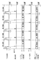
- FIG. 3 is a timing chart for explaining the operation of the generation unit 16.
- the five timing charts shown in FIG. 3 all have the same time axis as the horizontal axis, and the vertical axis shows the signal level of the PWM signal and the interrupt processing executed according to the PWM signal from the top of the figure.
- the execution state, the contents of the register buffer 161 or 162 of the generation unit 16, the on / off state of the load signal for loading the contents of the register buffers 161 and 162 into the period register 163 and the duty register 164, and the period register 163 or the duty The contents of register 164 are shown.
- the period and the fourth period, and the period from time t14 to t21 is the fourth period in the previous N period.
- the timing when the PWM signal rises coincides with the start time of each cycle.
- the falling edge when the signal level in each cycle of the PWM signal changes from H to L is accepted as an interrupt request to the interrupt controller 15 and the interrupt process is executed once.
- the interrupt processing is executed when the on-time T14, T21, T22, T23, and T24 in each cycle has elapsed from time t14, t21, t22, t23, and t24, respectively.
- the set value for each period and on-time for the next PWM period is read from the set value storage area 131 a or 131 b included in the RAM 13 and set in the register buffers 161 and 162.
- the on-time set value is set in the register buffer 162 only once in N cycles.
- the setting value storage area 131a (or 131b) is stored in the setting value storage area 131a (or 131b) for the N periods during which reading from the setting value storage area 131b (or 131a) is being performed. This is performed during N cycles preceding the cycle in which reading from 131a (or 131b) is started.
- the set values read from the set value storage area 131a (or 131b) in the fourth period, the first period, the second period, and the third period that are continuous from the time t14 are the fourth consecutive before the time t14. It is calculated during the period, the first period, the second period, and the third period, and is stored in the set value storage area 131a (or 131b).
- the setting values are read from the setting value storage area 131b (or 131a) during the fourth period, the first period, the second period, and the third period that precede the time t14.
- the set values for the first period, the second period, the third period, and the fourth period stored in the set value storage area 131a are the fourth consecutive values after each set value is stored.
- the data are sequentially read out by the interrupt processing in the period, the first period, the second period, and the third period, and set in the register buffers 161 and 162.
- the contents of the register buffers 161 and 162 correspond to the first period, the second period, the third period, and the third period. It is rewritten to the set value for 4 cycles.
- the PWM signal generation unit 165 applies to the period register 163 and the duty register 164, respectively.
- a load signal for loading the contents of the register buffers 161 and 162 is provided.
- the contents of the period register 163 and the duty register 164 correspond to the first period, the second period, the third period, and the It is held at the set value for 4 cycles.
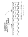
- FIG. 4 is an explanatory diagram for explaining an operation in which an average duty of a PWM signal is determined by a set value for N cycles.
- the horizontal axis represents time
- the vertical axis represents the signal level of the PWM signal.
- FIG. 4 shows how the PWM signals in the first, second, third, and fourth periods of the PWM period change on / off for two consecutive N periods.
- the PWM signal in each PWM cycle is on in the first half and off in the second half.
- N 4 for simplicity
- the standard period (hereinafter referred to as the reference period) of the PWM signal generated by the generation unit 16 is 10 ⁇ s
- the minimum unit of the settable value for each of the period and the on time that can be set in the generation unit 16 (Ie, the smallest increment) is 1, and this minimum unit of 1 corresponds to 1 ⁇ s of the period and the on-time of the PWM signal.
- the period and on-time of the PWM signal generated by the generation unit 16 can be set in increments of 1 ⁇ s.
- the minimum unit of the target duty calculated by the CPU 11 by the PID calculation is 0.1%.
- the target duty is 52.0% as a result of the PID calculation in the previous N cycles at the timing shown in FIG.
- the duty of the PWM signal is 50.0% (or 60.0%). It becomes.
- the set values of the PWM signal cycle and on-time are set to 9 (or 11) and 5, respectively, the duty of the PWM signal is 55.6% (or 45.5%).
- the duty of the PWM signal changes approximately in units of 10%, and the period is set.
- the duty of the PWM signal changes in units of about 5%, and a deviation from the target duty of 52.0% cannot be ignored.
- a set value of the on time that can obtain an on time close to the target on time corresponding to the target duty is determined.
- it is preferable to determine a set value of the on-time at which the on-time closest to the target on-time is obtained.
- a settable value of a cycle that can obtain a cycle close to a cycle obtained by multiplying a cycle determined by the on time obtained by the set value of the on time and the target duty by N is allocated to N set values as evenly as possible.
- the set value of the period for the next N periods is determined.
- it is preferable to determine a set value of a cycle at which a cycle closest to the above N times cycle is obtained.
- the target on-time corresponding to the target duty (52.0%) is 5.20 ⁇ , and thus the set value of the on-time is determined to be 5.
- a cycle in which a cycle closest to a cycle (38.46 ⁇ s) that is four times the cycle obtained by dividing the on-time (5 ⁇ s) obtained by the set value of the on-time by the target duty (0.520) is obtained.
- Is set to four set values, and the set value of the period is determined to be 10, 9, 10, 9, for example.
- the period of the PWM signal in each of the first period, the second period, the third period, and the fourth period in the next N periods is 10 ⁇ s, 9 ⁇ s, 10 ⁇ s, and 9 ⁇ s
- the on-time is uniformly 5 ⁇ s. That is, the added value of the period over the first period, the second period, the third period, and the fourth period is 38 ⁇ s, the added value of the on-time is 20 ⁇ s, and the average of duty for N periods based on these added values The value becomes 52.63%, indicating that the deviation from the target duty of 52.0% falls within 0.63%.
- the set value of the above-described cycle may be determined as 10, 10, 9, 9, or may be determined as 9, 10, 9, 10, for example.
- the combination of the set values 10 and 9 may be arbitrarily determined according to the purpose of suppressing voltage fluctuation.
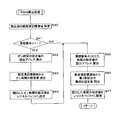
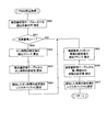
- FIG. 5 is a flowchart showing a processing procedure of the CPU 11 that executes the periodic interrupt processing in the signal generation circuit 1 according to the first embodiment of the present invention
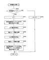
- FIG. 6 shows a processing procedure of the CPU 11 according to the setting value determination subroutine. It is a flowchart which shows.
- the RAM 13 stores the cycle number J in FIG. 5, information indicating which of the set value storage areas 131a and 131b is for storage (or read-out), and the cycle counter L in FIG.
- the initial value of the cycle number J is N.
- the set values for the period and the on-time corresponding to the N periods determined in the process of FIG. 6 are sequentially stored in consecutive addresses in the set value storage area 131a or 131b.
- the periodic interrupt that triggers the periodic interrupt process shown in FIG. 5 occurs at the start of each period included in the N period. For example, the period interrupt may be generated at the rising edge of the PWM signal generated by the generation unit 16.
- the CPU 11 determines whether or not the periodic number J is N (here, 4) (S10). (S10: YES), J is set to 1 (S11), and the setting value storage areas 131a and 131b are switched between storing and reading (S12). For example, if the set value storage area 131b (or 131a) is for storage before the process of step S12, the set value storage area 131a (or 131b) is switched for storage in the process of step S12, and the set value storage is performed. The area 131b (or 131a) is switched for reading.
- the set value storage area 131a (or 131b) switched for storage in step S12 is an area for storing set values for each of N periods and on-times determined in the set value determination subroutine.
- the setting value storage area 131b (or 131a) switched for reading is an area from which setting values are read out in a PWM interrupt process described later.
- the CPU 11 takes in an output voltage value obtained by converting the output voltage supplied to the load 4 by the A / D converter 14 (S13), and performs voltage loop control based on the taken-in voltage value and the voltage target value.
- the calculation is executed (S14), and the target value of the current is calculated as the operation amount.
- the CPU 11 takes in the output current value obtained by converting the detection voltage of the current detector 27 by the A / D converter 14 (S15), and calculates the current loop control based on the taken-in current value and the current target value. Is executed (S16), and a target duty is calculated as an operation amount (corresponding to a third calculation unit). In order to omit the current loop control, steps S15 and S16 may not be executed. When steps S15 and S16 are not executed, the value calculated in step S14 is the target duty.
- the CPU 11 calls and executes a subroutine related to setting value determination (S17), and then returns to the interrupted routine.
- the CPU 11 increments J by 1 (S18), and then returns to the interrupted routine. That is, every time the periodic interruption occurs N times, the processing from step S11 to S17 is executed once, and the set values for the period and the on-time for N periods are determined.
- the CPU 11 multiplies the reference period of the PWM signal generated by the generation unit 16 and the target duty calculated in step S14.
- the setting value of the on time for generating the PWM signal having the on time closest to the on time corresponding to is generated in the generating unit 16 (S20: corresponding to the first determining unit).
- the target duty is 52.0%
- the target on-time is 5.20 ⁇ s with respect to the reference period of 10 ⁇ s, and the on-time of 5 ⁇ s, which is the actual on-time closest thereto.
- the on-time setting value for causing the generator 16 to generate the PWM signal having the following is determined to be 5.
- the CPU 11 stores the determined on-time set value in the set value storage area 131a or 131b (S21). Which of the set value storage areas 131a and 131b is for storage is specified by the switching process in step S12 shown in FIG.
- the CPU 11 multiplies the period corresponding to the result of dividing the on-time of the PWM signal generated according to the determined on-time setting value by the target duty by N and calculates the total for N periods (S22). : Equivalent to the first calculation unit), and a settable value of a cycle for generating a PWM signal having a cycle closest to the calculated total of N cycles is specified (S23: corresponding to the specification unit).
- S23 corresponding to the specification unit.
- the ON time of the generated PWM signal is 5 ⁇ s and the target duty is 52.0%
- the CPU 11 calculates the quotient Q and the remainder R by dividing the specified settable value by N (S24: corresponding to the second calculation unit).
- the settable value 38 is divided by 4
- the quotient Q is calculated as 9
- the remainder R is calculated as 2.
- the CPU 11 temporarily stores all the set values for the N cycles as Q in the set value storage area 131a or 131b (S25).
- Q corresponds to a reference value of a period settable value.
- Which of the set value storage areas 131a and 131b is for storage is specified by the switching process in step S12 shown in FIG.
- the CPU 11 initializes the cycle counter L to 1 (S26).
- the CPU 11 determines whether or not the remainder R calculated in step S24 (R as a calculation result in step S29 when step S29 described later is executed) is 0 (S27). If so (S27: YES), the process returns to the called routine.
- R is 0 means that the process of dividing the remainder R of the division result into the minimum unit of the period settable value and adding it to a part of the reference value is completed, or that the remainder R to be divided into the minimum unit is Means zero from the beginning
- the CPU 11 sets the set value of the cycle of the Lth cycle as an added value of the quotient Q and the minimum unit of the settable value of the cycle (S28), and has already been set value storage area
- the period setting value (Q) stored in 131a or 131b is overwritten.
- the process in step S28 is a process of incrementing the set value of the period stored in the set value storage area 131a or 131b by 1. It can be replaced.
- the CPU 11 newly sets a value obtained by subtracting the minimum unit of the period settable value from R as R (S29), increments the period counter L by 1 (S30), and moves the process to step S27.
- R the minimum unit of the period settable value
- S30 increments the period counter L by 1
- FIG. 7 is a flowchart showing a part of another processing procedure of the CPU 11 according to the setting value determination subroutine. The process shown in FIG. 7 is executed as a process subsequent to step S25 shown in FIG.
- step S25 shown in FIG. 6 the CPU 11 stores the set value (Q) for the N cycles in the set value storage area 131a or 131b (S25), and then the remainder R calculated in step S24 is 0. Whether or not (S31: YES), the process returns to the called routine.
- step S31 the CPU 11 determines whether or not R is 1 (S32).
- R is 1 (S32: YES)
- the set value of the cycle of the first cycle Is overwritten as an addition value of the quotient Q and the minimum unit of the period settable value (S33), and the process returns to the called routine.
- step S33 the set value of the period of the second period, the third period, or the fourth period may be overwritten.
- the CPU 11 determines whether or not R is 2 (S34), and when R is 2 (S34: YES), the set value of the cycle of the first cycle Is overwritten as the addition value of the quotient Q and the minimum unit of the settable value of the period (S35), and the set value of the period of the third period is added to the minimum unit of the settable value of the period Q
- the value is overwritten (S36), and the process returns to the called routine.
- steps S35 and S36 for example, the setting values of the second and fourth periods may be overwritten, or the setting values of the first and fourth periods may be overwritten.
- FIG. 8 is a chart showing a list of set values for the period and on-time for N periods determined according to the target duty.
- the target duty (%) is represented by a numerical value of one or two decimal places.
- a combination of the set values may be arbitrarily determined.
- the set value of the period for N cycles is determined as 9, 8, 9, 8, and the set value of the on time is set to 3. It is determined. In this case, the average value of the duty over N cycles is 35.29%.
- the set value of the cycle for N cycles is determined as 12, 11, 12, and 11, and the set value of the on time is determined as 4. Is done. In this case, the average value of the duty over N cycles is 34.78%.
- the set value of the cycle for N cycles is determined as 9, 9, 9, 9, and the set value of the on time is determined as 4. Is done. In this case, the average value of the duty over N cycles is 44.44%.
- the set value of the cycle for N cycles is determined as 11, 11, 11, and 11 and the set value of the on time is determined as 5. Is done. In this case, the average value of the duty over N cycles is 45.45%.
- the target duty is within the range of 45.98% to 47.05%
- the set value of the period for N cycles is determined as 11, 11, 11, and 10 and the set value of the on time is determined as 5. Is done. In this case, the average value of the duty over N cycles is 46.51%.
- the set value of the period for N cycles is determined as 11, 10, 11, 10, and the set value of the on time is determined as 5. Is done. In this case, the average value of duty over N cycles is 47.62%.
- the set value of the period for N cycles is determined as 11, 10, 10, and 10 and the set value of the on-time is determined as 5. Is done. In this case, the average value of the duty over N cycles is 48.78%.
- the set value of the period for N cycles is determined as 10, 10, 10, and 10 and the set value of the on-time is determined as 5. Is done. In this case, the average value of the duty over N cycles is 50.00%.
- the set value of the cycle for N cycles is determined as 10, 10, 10, 9, and the set value of the on time is determined as 5. Is done. In this case, the average value of the duty over N cycles is 51.28%.
- the set value of the cycle for N cycles is determined as 10, 9, 10, 9, and the set value of the on-time is determined as 5. Is done. In this case, the average value of the duty over N cycles is 52.63%.
- the set value of the cycle for N cycles is determined as 10, 9, 9, 9, and the set value of the on-time is determined as 5. Is done. In this case, the average value of the duty over N cycles is 54.05%.
- the set value of the cycle for N cycles is determined to be 9, 9, 9, 9, and the set value of the on time is determined to be 5. Is done. In this case, the average value of the duty over N cycles is 55.56%.
- the set value of the cycle for N cycles is determined as 11, 11, 11, and 11 and the set value of the on time is determined as 6. Is done. In this case, the average value of the duty over N cycles is 54.55%.
- FIG. 9 is a flowchart showing a processing procedure of the CPU 11 that executes the PWM interrupt processing in the signal generation circuit 1 according to the first embodiment of the present invention.
- the cycle number J in FIG. 9 is a number that is updated by the cycle interrupt process shown in FIG. 5 and is stored in the RAM 13.
- the PWM interrupt that triggers the PWM interrupt processing shown in FIG. 9 occurs at the falling edge of the PWM signal generated by the generator 16 shown in FIG.
- the CPU 11 specifies the setting value storage area for reading out of the setting value storage areas 131a and 131b (S40). Thereafter, the CPU 11 determines whether or not the cycle number J is 1 (S41), and if it is 1 (S41: YES), the CPU 11 sets the set value of the on time in the specified set value storage area 131a (or 131b). A read address is calculated (S42). The read address here corresponds to the storage address of the set value of the on time in step S21 of the set value determination subroutine shown in FIG.
- the CPU 11 reads the set value of the on-time from the specified set value storage area 131a (or 131b) (S43), and sets the read set value in the register buffer 162 of the generation unit 16 (S44).
- the CPU 11 sets the read address of the cycle set value in the specified set value storage area 131a (or 131b) as the cycle number J. (S45).
- the read address here corresponds to the storage address of the cycle set value in steps S25 and S28 of the set value determination subroutine shown in FIG.
- the CPU 11 reads one set value of the period corresponding to the Jth cycle from the specified set value storage area 131a (or 131b) (S46), and sets the read set value in the register buffer 161 of the generation unit 16. (S47), the process returns to the interrupted routine.
- the CPU 11 multiplies the period obtained by dividing the on-time of the PWM signal generated by the generating unit 16 by the target duty according to the determined set value of the on-time by N, and the period multiplied by N
- a settable value of a cycle for generating a PWM signal having a cycle closest to the value is specified, and a set value of a cycle for N cycles is determined based on a quotient Q and a remainder R obtained by dividing the specified settable value by N. It is determined and set in the generator 16 one by one for each period of the PWM signal.
- the CPU 11 determines and sets the average duty over the N cycles of the PWM signal generated by the generator 16 so as to be close to the target duty for the set value of the N cycles set in the generator 16. Therefore, the average value for the entire set value of the period of N cycles is finely adjusted with respect to the minimum unit (that is, the minimum increment) of the set value of the period. Therefore, it is possible to make the minimum unit of the value set in the generating unit 16 that generates a signal having a cycle and on-time corresponding to the set value substantially smaller than the actual minimum unit.
- the quotient Q of the above-described division result is specified as a reference value for the entire set value of the period for N cycles, and the remainder R of the above-described division result is set to the settable value of the period. It divides
- segmented minimum unit is added to a part of reference value for N period, respectively, and the setting value of the period for N period is determined. Therefore, the value ( 1) obtained by dividing the remainder R into the minimum unit is appropriately distributed to the set value of the cycle for N cycles, and a part of the set value of the cycle for N cycles is used as the reference. It is possible to determine the value obtained by adding the value of the minimum unit of the period settable value to the value, and to determine the set value of the other period excluding a part of the set value as the reference value.
- the set values for the determined N cycles and the on-time are once stored in the set value storage area 131a or 131b included in the RAM 13, and then sequentially read out in the PWM cycle.
- the set values for the period and the on-time for N cycles are determined from the contents stored in advance in the set value storage table 121 included in the ROM 12, and are sequentially read out in the PWM cycle. It is a form.
- the configurations of the voltage conversion device and the signal generation circuit 1 in the second embodiment are the same as those shown in FIGS. 1 and 2 in the first embodiment. However, in the second embodiment, the set value storage areas 131a and 131b included in the RAM 13 are not used.
- the setting value storage table 121 included in the ROM 12 a plurality of sets of setting values for each of the N periods and the on-time respectively associated with the target duty ranges shown in FIG. Has been.
- the set value storage table 121 may be included in another memory outside the control unit 10. From the set values for each of the N periods and on-times stored in the set value storage table 121 in a plurality of sets, the setting for each set of N periods and on-times is performed in the interrupt processing for each N period. The value is determined.
- the timing chart showing the operation of the generating unit 16 in the second embodiment is the same as that shown in FIG. 3 in the first embodiment.
- the operation in which the average duty of the PWM signal is determined by the set values of the period and the on-time for N cycles in the signal generation circuit 1 according to the second embodiment is the same as in the explanatory diagram shown in FIG. 4 in the first embodiment.
- symbol is attached
- the set values for the period and on-time determined for N periods determined from the contents stored in the set value storage table 121 are the fourth period, the first period, the second period, and the like, which are continuous after each set value is determined.
- the data is sequentially read out by the interrupt processing in the third period and set in the register buffers 161 and 162.
- FIG. 10 is a flowchart showing a processing procedure of the CPU 11 that executes periodic interrupt processing in the signal generation circuit 1 according to the second embodiment of the present invention
- FIG. 11 shows signal generation according to the second embodiment of the present invention
- 3 is a flowchart showing a processing procedure of a CPU 11 that executes PWM interrupt processing in a circuit 1; The trigger for the occurrence of these interrupt processes is the same as in the first embodiment.
- steps S50 to S58 shown in FIG. 10 the processes except for steps S52 and S57 are the same as the processes from steps S10 to S18 shown in FIG. The part is omitted.
- step S60 to S67 shown in FIG. 11 is similar to the process from step S40 to S47 shown in FIG. 9 in the first embodiment, a part of the description is simplified.
- the CPU 11 determines whether or not the periodic number J is N (here, 4) (S50). (S50: YES), J is set to 1 (S51), and the row to be read in the set value storage table 121 is fixed to the row determined in the previous periodic interrupt process (see step S57 described later) (S52). Thereafter, the CPU 11 calculates a target duty (corresponding to the third calculation unit) by executing a calculation related to the voltage loop control based on the output voltage and the current loop control based on the output current (S53 to S56).
- a target duty corresponding to the third calculation unit
- the CPU 11 collates the contents of the set value storage table 121, that is, each range of the target duty stored in the table with the target duty calculated by the above-described calculation, and determines a row to be read ( S57: Corresponding to the first and second determination units), and the process returns to the called routine.
- the set values for the period and the on-time corresponding to the N periods stored in the set value storage table 121 corresponding to the range including the target duty become the determined set values.
- the CPU 11 specifies a row to be read in the set value storage table 121 (S60). Thereafter, the CPU 11 determines whether or not the cycle number J is 1 (S61), and when it is 1 (S61: YES), the CPU 11 calculates a read address of the set value of the on-time in the specified set value storage table 121. Then, the set value of the on-time is read from the address calculated for the set value storage table 121 (S63), and the read set value is set in the register buffer 161 (S64).
- step S64 When the process of step S64 is completed, or when the cycle number J is not 1 (S61: NO), the CPU 11 calculates a read address of the set value of the cycle in the specified row according to the cycle number J (S65). Then, the set value for the Jth cycle is read from the calculated address (S66), the read set value is set in the register buffer 162 (S67), and the process returns to the interrupted routine.
- the value for N cycles of the set values for the predetermined period and the on-time are associated with the target duty and stored in the set value storage table 121. Yes.
- the CPU 11 determines from the stored information in the set value storage table 121 the N cycles of the set values for the cycle and on-time set in the generator 16 according to the target duty. Therefore, it is possible to easily determine the set values for the period and the on-time for N periods to be determined according to the target duty when the CPU 11 executes the control.
- the CPU 11 sequentially reads the set values for the period and the on-time from the set value storage table 121 every N periods of the PWM control and sets them in the generation unit 16. Accordingly, the contents of the set value storage table 121 can be sequentially set in the generation unit 16 over N cycles.
- the voltage conversion circuit 2 converts the voltage by switching according to the duty of the PWM signal generated by the signal generation circuit 1, and the PWM control based on the converted voltage
- the CPU 11 of the signal generation circuit 1 calculates the target duty described above. Therefore, the signal generating circuit 1 capable of making the minimum unit of the value set in the generating unit 16 that periodically generates the PWM signal substantially smaller than the actual minimum unit is applied to the voltage converter and output. It becomes possible to improve the accuracy of the voltage.
Landscapes
- Engineering & Computer Science (AREA)
- Power Engineering (AREA)
- Dc-Dc Converters (AREA)
Abstract
設定された値に応じた周期及びオン時間を有する信号を発生する発生部に設定する値の最小単位を実際の最小単位よりも実質的に小さくすることが可能な信号発生回路、電圧変換装置及び信号発生方法を提供する。CPU11は、発生部16が発生するPWM信号のN周期毎に、基準周期及び目標のデューティの積に相当するオン時間に最も近いオン時間を有するPWM信号を発生部16に発生させるオン時間の設定値を決定して発生部16に設定する。更に、CPU11は、決定したオン時間の設定値に応じて発生部16が発生するPWM信号のオン時間を目標のデューティで除算して得た周期をN倍し、N倍した周期に最も近い周期を有するPWM信号を発生させる周期の設定可能値を特定し、特定した設定可能値をNで除算して得た商Q及び剰余Rに基づいてN周期分の周期の設定値を決定して、PWM信号の周期毎に発生部16に設定する。
Description
本発明は、設定された値に応じた周期及びオン時間を有する信号を発生する発生部と、目標のデューティに応じて発生部に設定可能な周期及びオン時間夫々の設定可能値を設定する制御部とを備える信号発生回路、電圧変換装置及び信号発生方法に関する。
従来、スイッチング素子をPWM(Pulse Width Modulation )信号で駆動することによって電圧を変換する電圧変換装置が広く利用されている。このPWM制御方式の電圧変換装置では、例えば電圧の目標値に基づいて電圧指令値を算出し、算出した電圧指令値に応じた値をPWM信号の発生部に設定することによって、設定された値に応じたデューティを有するPWM信号を発生する。このように、スイッチング素子を駆動するPWM信号のデューティを電圧の目標値に応じて変化させることにより、電圧の目標値に応じた出力電圧が得られる。
ここで、PWM信号の発生部に設定可能な値(以下、設定可能値という)の最小単位(即ち最小の増分)が比較的大きい場合は、目標値の変化に対してPWM信号のデューティを滑らかに変化させることができなくなり、出力電圧が階段状に変化することとなる。また例えば、PWM制御による操作量としてPWM信号の発生部に設定すべき目標の値が算出される場合、目標の値の最小単位よりも設定可能値の最小単位の方が大きいときは、電圧の目標値の変化及び負荷変動に対してPWM信号のデューティを滑らかに変化させることができなくなり、出力電圧に誤差が生じる。
これに対し、特許文献1には、PWM信号のオン/オフ時間をPWM制御の周期毎に演算する際に、電圧指令値を被除数とする除算の剰余を切り捨てて演算することによってオン/オフ時間を算出し、算出結果に基づいてPWMパルスを出力するPWMインバータが開示されている。上記の演算で生じた剰余は、オン/オフ時間に反映されずに切り捨てられた電圧指令値に相当する。
このPWMインバータでは、切り捨てた剰余を次の周期以降の演算における電圧指令値に順次加算することにより、前回の演算でオン/オフ時間に反映されなかった剰余が次回の演算の際に新たなオン/オフ時間に反映され、その際の剰余が更に次の演算に反映されることが繰り返される。このため、PWM信号の発生部に対して設定されるオン/オフ時間の平均値を、本来設定されるべき目標のオン/オフ時間に近づけることができる。つまり、発生部に設定される値の最小単位を、平均的には実際の最小単位よりも小さくすることができる。
しかしながら、特許文献1に開示された技術では、PWM制御の周期毎に除算を含む演算を実行してPWM信号のオン/オフ時間を決定するため、周期毎に多大な処理負荷が発生する。このため、処理能力が低い安価なマイクロコンピュータでは、上記の演算処理をPWM制御の1周期内で完了させることができない虞があった。
本発明は斯かる事情に鑑みてなされたものであり、その目的とするところは、設定された値に応じた周期及びオン時間を有する信号を発生する発生部に設定する値の最小単位を実際の最小単位よりも実質的に小さくすることが可能な信号発生回路、電圧変換装置及び信号発生方法を提供することにある。
本発明の一態様に係る信号発生回路は、設定された値に応じた周期及びオン時間を有する信号を発生する発生部と、目標のデューティに応じて前記発生部に設定可能な周期及びオン時間夫々の設定可能値を設定する制御部とを備え、前記発生部は、外部の電圧変換回路に対してPWM信号を発生させ、前記電圧変換回路をPWM制御することにより電圧を変換させる信号発生回路において、前記制御部は、前記信号のN周期(Nは2以上の自然数)毎に、所定の周期及び前記目標のデューティの積に近いオン時間を有する信号を発生させるように、前記発生部に設定するオン時間の設定可能値を決定する第1決定部と、該第1決定部が決定したオン時間の設定可能値に応じて発生する信号のオン時間を前記目標のデューティで除して得られる周期のN周期分の総和を算出する第1算出部と、該第1算出部が算出した総和に近い周期を有する信号を発生させる周期の設定可能値を特定する特定部と、該特定部が特定した周期の設定可能値をNで除して商及び剰余を算出する第2算出部と、該第2算出部が算出した商及び剰余に基づいて、前記発生部に設定するN周期分の周期の設定可能値を決定する第2決定部とを有することを特徴とする。
本発明の一態様に係る信号発生回路は、前記第2決定部は、前記商を前記周期の設定可能値の基準値に特定し、前記剰余を前記周期の設定可能値の最小単位に分割してN周期分の基準値の一部に夫々加算することによりN周期分の設定可能値を決定するようにしてあることを特徴とする。
本発明の一態様に係る信号発生回路は、所定のデューティとN周期分の周期及びオン時間夫々の設定可能値とを対応付けて記憶する記憶部を備え、前記第1及び第2決定部は、前記所定のデューティに対応するN周期分の周期及びオン時間夫々の設定可能値を前記記憶部の記憶情報から決定するようにしてあることを特徴とする。
本発明の一態様に係る信号発生回路は、前記制御部は、前記第2決定部が決定したN周期分の周期及びオン時間夫々の設定可能値を前記記憶部から読み出して前記発生部に設定するようにしてあることを特徴とする。
本発明の一態様に係る電圧変換装置は、上述の信号発生回路と、該信号発生回路が発生した信号のデューティに応じたスイッチングによって電圧を変換する電圧変換回路と、該電圧変換回路が変換した電圧を検出する検出部とを備える電圧変換装置であって、前記信号発生装置が備える制御部は、前記検出部が検出した電圧に基づいて前記目標のデューティを算出する第3算出部を有することを特徴とする。
本発明の一態様に係る信号発生方法は、設定された値に応じた周期及びオン時間を有する信号を発生する発生部と、目標のデューティに応じて前記発生部に設定可能な周期及びオン時間夫々の設定可能値を設定する制御部とを備え、前記発生部は、外部の電圧変換回路に対してPWM信号を発生させ、前記電圧変換回路をPWM制御することにより電圧を変換させる信号発生回路で前記信号を発生させる方法において、前記信号のN周期(Nは2以上の自然数)毎に、所定の周期及び前記目標のデューティの積に近いオン時間を有する信号を発生させるように、前記発生部に設定するオン時間の設定可能値を決定し、決定したオン時間の設定可能値に応じて発生する信号のオン時間を前記目標のデューティで除して得られる周期のN周期分の総和を算出し、算出した総和に近い周期を有する信号を発生させる周期の設定可能値を特定し、特定した設定可能値をNで除して商及び剰余を算出し、算出した商及び剰余に基づいて、前記発生部に設定するN周期分の周期の設定可能値を決定することを特徴とする。
本態様にあっては、制御部は、目標のデューティに応じて発生部に設定可能な周期及びオン時間夫々の設定可能値を決定して発生部に設定する。ここでの設定可能値は、発生部に設定可能な値の最小単位の整数倍の値である。具体的には、制御部は、発生部が発生する信号のN周期毎に、所定の周期及び目標のデューティの積に相当するオン時間に近いオン時間を有する信号を発生部に発生させるオン時間の設定可能値を決定し、決定したオン時間の設定可能値を発生部に設定する。これと並行して、制御部は、決定したオン時間の設定可能値に応じて発生部が発生する信号のオン時間を目標のデューティで除して得た周期をN倍し、N倍した周期に近い周期を有する信号を発生させる周期の設定可能値を特定し、特定した設定可能値をNで除算して得た商及び剰余に基づいてN周期分の周期の設定可能値を決定して、上記信号の周期毎に1つずつ発生部に設定する。
これにより、制御部が決定して発生部に設定するN周期分の周期の設定可能値について、発生部が発生する信号のN周期にわたる平均的なデューティが目標のデューティに近くなるように決定されるため、N周期分の周期の設定可能値全体についての平均的な値が、周期の設定可能値の最小単位(即ち最小の増分)よりもきめ細かく調整される。
これにより、制御部が決定して発生部に設定するN周期分の周期の設定可能値について、発生部が発生する信号のN周期にわたる平均的なデューティが目標のデューティに近くなるように決定されるため、N周期分の周期の設定可能値全体についての平均的な値が、周期の設定可能値の最小単位(即ち最小の増分)よりもきめ細かく調整される。
本態様にあっては、上述の除算結果の商を、N周期分の周期の設定可能値全体についての基準値に特定し、上述の除算結果の剰余を周期の設定可能値の最小単位(即ち最小の増分)に分割し、分割した最小単位の値をN周期分の基準値の一部に夫々加算してN周期分の周期の設定可能値を決定する。
これにより、上記剰余を最小単位に分割した値が、N周期分の周期の設定可能値に適当に配分されることとなり、N周期分の周期の設定可能値の一部が上記基準値に周期の設定可能値の最小単位の値を加えた値と決定され、上記設定可能値の一部を除く他の設定可能値が上記基準値と決定される。
これにより、上記剰余を最小単位に分割した値が、N周期分の周期の設定可能値に適当に配分されることとなり、N周期分の周期の設定可能値の一部が上記基準値に周期の設定可能値の最小単位の値を加えた値と決定され、上記設定可能値の一部を除く他の設定可能値が上記基準値と決定される。
本態様にあっては、予め決定された周期及びオン時間夫々の設定可能値のN周期分の値と目標のデューティとが対応付けられて記憶部に記憶されている。制御部は、目標のデューティに応じて、発生部に設定する周期及びオン時間夫々の設定可能値のN周期分を記憶部の記憶情報から決定する。
これにより、目標のデューティに応じて決定すべきN周期分の周期及びオン時間夫々の設定可能値が、制御部による制御の実行時に容易に決定される。
これにより、目標のデューティに応じて決定すべきN周期分の周期及びオン時間夫々の設定可能値が、制御部による制御の実行時に容易に決定される。
本態様にあっては、制御部は、記憶部から周期及びオン時間夫々の設定可能値をN周期毎に順次読み出して発生部に設定する。
これにより、記憶部の内容が、N周期にわたって順次発生部に設定される。
これにより、記憶部の内容が、N周期にわたって順次発生部に設定される。
本態様にあっては、上述の信号発生回路が発生した信号のデューティに応じたスイッチングによって電圧変換回路が電圧を変換し、変換された電圧に基づいて、信号発生回路の制御部が上述の目標のデューティを算出する。
これにより、信号を周期的に発生する発生部に設定する値の最小単位を実際の最小単位よりも実質的に小さくすることが可能な信号発生回路が電圧変換装置に適用されて、出力電圧の精度が向上する。
これにより、信号を周期的に発生する発生部に設定する値の最小単位を実際の最小単位よりも実質的に小さくすることが可能な信号発生回路が電圧変換装置に適用されて、出力電圧の精度が向上する。
上記によれば、制御部が決定して発生部に設定するN周期分の周期の設定可能値について、発生部が発生する信号のN周期分の平均的なデューティが目標のデューティに近くなるように決定されるため、N周期分の周期の設定可能値全体についての平均的な値が、周期の設定可能値の最小単位(即ち最小の増分)よりもきめ細かく調整される。
従って、設定された値に応じた周期及びオン時間を有する信号を発生する発生部に設定する値の最小単位を実際の最小単位よりも実質的に小さくすることが可能となる。
従って、設定された値に応じた周期及びオン時間を有する信号を発生する発生部に設定する値の最小単位を実際の最小単位よりも実質的に小さくすることが可能となる。
以下、本発明をその実施の形態を示す図面に基づいて詳述する。
(実施の形態1)
図1は、本発明の実施の形態1に係る電圧変換装置の構成例を示すブロック図であり、図2は、本発明の実施の形態1に係る信号発生回路の一部の構成例を示すブロック図である。図中1は信号発生回路であり、信号発生回路1は、周期及びオン時間が変化するPWM信号を発生して電圧変換回路2に与える。電圧変換回路2は、外部のバッテリ3の電圧を変換して外部の負荷4に供給する。ここでは電圧変換回路2がバッテリ3の電圧を降圧するが、バッテリ3の電圧を昇圧又は昇降圧するものであってもよい。
(実施の形態1)
図1は、本発明の実施の形態1に係る電圧変換装置の構成例を示すブロック図であり、図2は、本発明の実施の形態1に係る信号発生回路の一部の構成例を示すブロック図である。図中1は信号発生回路であり、信号発生回路1は、周期及びオン時間が変化するPWM信号を発生して電圧変換回路2に与える。電圧変換回路2は、外部のバッテリ3の電圧を変換して外部の負荷4に供給する。ここでは電圧変換回路2がバッテリ3の電圧を降圧するが、バッテリ3の電圧を昇圧又は昇降圧するものであってもよい。
信号発生回路1は、CPU(Central Processing Unit )11を有するマイクロコンピュータである。CPU11は、プログラム等の情報を記憶するROM(Read Only Memory )12、一時的に発生した情報を記憶するRAM(Random Access Memory )13、アナログの電圧をデジタル値に変換するA/D変換器(検出部に相当)14、複数の割込要求を処理する割込コントローラ15、及びPWM信号を発生する発生部16と互いにバス接続されている。信号発生回路1のうち、発生部16を除いたものが制御部10であるが、発生部16が制御部10に含まれていてもよい。
割込コントローラ15は、複数の割込要求を受け付け可能に構成されており、何れかの割込要求を受け付けた場合、CPU11に対してインタラプトを要求する信号(所謂INT信号)を与え、CPU11からアクノレッジ信号(所謂INTA信号)が与えられたときに、各割込要求に対応する割込ベクタをバスに送出する。バスに送出された割込ベクタがCPU11に読み込まれた場合、CPU11が各割込要求に対応する割込処理を実行するようになっている。
電圧変換回路2は、ドレインがバッテリ3の正極端子に接続されたNチャネル型のMOSFET(Metal Oxide Semiconductor Field Effect Transistor:以下、単にFETという)21と、該FET21のソース及びバッテリ3の負極端子夫々にドレイン及びソースが接続されたFET22と、発生部16から与えられたPWM信号に基づいてFET21及びFET22夫々のゲートに駆動信号を与える駆動回路26とを備える。
FET22のドレイン及びソース間には、インダクタ23及び抵抗器24の直列回路を介して負荷4が接続されている。負荷4には、コンデンサ25が並列に接続されている。抵抗器24及びコンデンサ25の接続点の電圧が、A/D変換器14に与えられる。抵抗器24の両端には電流検出器27が接続されており、電流検出器27の検出電圧がA/D変換器14に与えられる。
図2に移って、ROM12は、後述する目標のデューティに対応付けて予め決定された複数の設定値を記憶する設定値記憶テーブル(記憶部に相当)121を含む。但し、本実施の形態1では、設定値記憶テーブル121を用いない。
RAM13は、複数の設定値の記憶及び読み出しを各別のタイミングで行うために二重化された設定値記憶領域131a及び131bを含む。設定値記憶領域131a(又は131b)に記憶された設定値は、割込コントローラ15が調停する後述の割込処理にて、順次発生部16に設定されるようになっている。
発生部16は、後述する周期及びオン時間夫々の設定値が設定されるレジスタバッファ161及び162と、レジスタバッファ161及び162夫々の内容が周期的にロードされる周期レジスタ163及びデューティレジスタ164と、周期レジスタ163及びデューティレジスタ164夫々の内容に応じた周期及びオン時間を有するPWM信号を生成するPWM信号生成部165とを有する。PWM信号生成部165は、周期レジスタ163及びデューティレジスタ164夫々に対してレジスタバッファ161及び162の内容をロードするためのロード信号を与える。
PWM信号生成部165は、不図示の内部クロックと、周期レジスタ163及びデューティレジスタ164夫々の内容とに基づいて、内部クロックの周期の整数倍の周期及びオン時間を有するPWM信号を生成する。PWM信号生成部165が生成したPWM信号は、駆動回路26に与えられると共に、割込要求の1つとして割込コントローラ15に与えられる。
上述の構成において、信号発生回路1のCPU11は、例えば電圧ループ制御及び電流ループ制御を並列的に実行する電流モード制御方式によって負荷4に供給する電圧を制御する。電圧ループ制御では、CPU11は負荷4に供給された出力電圧をA/D変換器14で変換したデジタル値を、目標の電圧値から減算した偏差に基づいて、後段の電流ループ制御で目標の電流値となる操作量を演算する。この電圧ループ制御では、電圧変換回路2が出力する電圧が制御量である。
電流ループ制御では、CPU11は電流検出器27の検出電圧をA/D変換器14で変換したデジタル値を、前段の電圧ループ制御からの目標の電流値から減算した偏差に基づいて、発生部16に対する操作量を演算する。CPU11は更に、演算した操作量(以下、目標のデューティという)に応じて発生部16に設定可能な周期及びオン時間夫々の設定可能値を決定する。ここでいう設定可能値とは、発生部16に設定されたときに出力のPWM信号の変化に反映される最小単位(最小の増分)の整数倍の値をいう。以下、簡単のため、発生部16に設定すべく決定された設定可能値を設定値という。発生部16は、決定された周期及びオン時間夫々の設定値が設定されることにより、設定値に応じた周期及びデューティを有するPWM信号を発生する。この電流ループ制御では、電圧変換回路2が出力する電流が制御量である。
ここで、電圧変換装置の出力電圧及び出力電流が時間的に比較的穏やかに変動する場合、上記の電圧ループ制御及び電流ループ制御の制御周期をPWM周期のN倍(Nは2以上の自然数)の周期で行っても十分であると言える。そこで本実施の形態1では、PWM周期のN周期毎に発生部16に対するN周期分の周期及びオン時間夫々の設定値をまとめて決定して設定値記憶領域131a又は131bに記憶しておき、PWM周期で発生する割込処理にて周期及びオン時間夫々の設定値を発生部16に設定する。
以下では、簡単のためにN=4とするが、これに限定されるものではなく、Nは2、3又は5以上であってもよい。また、N周期分の設定値は必ずしも周期毎に発生部16に設定する必要はなく、ある周期と次の周期とで周期及びオン時間夫々の設定値の少なくとも一方が変わるときにのみ設定するようにしてもよい。
次に、PWM信号生成部165が周期レジスタ163及びデューティレジスタ164夫々の内容に応じた周期及びオン時間を有するPWM信号を生成する仕組みについて説明する。
図3は、発生部16の動作を説明するためのタイミング図である。図3に示す5つのタイミング図は、何れも同一の時間軸を横軸としてあり、縦軸には、図の上から、PWM信号の信号レベル、PWM信号に応じて実行される割込処理の実行状態、発生部16のレジスタバッファ161又は162の内容、レジスタバッファ161及び162夫々の内容を周期レジスタ163及びデューティレジスタ164にロードするためのロード信号のオン/オフ状態、並びに周期レジスタ163又はデューティレジスタ164の内容を示してある。
図3は、発生部16の動作を説明するためのタイミング図である。図3に示す5つのタイミング図は、何れも同一の時間軸を横軸としてあり、縦軸には、図の上から、PWM信号の信号レベル、PWM信号に応じて実行される割込処理の実行状態、発生部16のレジスタバッファ161又は162の内容、レジスタバッファ161及び162夫々の内容を周期レジスタ163及びデューティレジスタ164にロードするためのロード信号のオン/オフ状態、並びに周期レジスタ163又はデューティレジスタ164の内容を示してある。
PWM信号は、時刻t21からt22まで、時刻t22からt23まで、時刻t23からt24まで、及び時刻t24からt31までの夫々が、N周期(N=4)における第1周期、第2周期、第3周期、及び第4周期であり、時刻t14からt21までが、1つ前のN周期における第4周期である。PWM信号が立ち上がるタイミングは、各周期の開始時点と一致している。PWM信号の各周期における信号レベルがHからLに変化する時の立ち下がりが、割込コントローラ15に対する割込要求として受け付けられて割込処理が1回実行される。
具体的には、時刻t14、t21、t22、t23及びt24夫々から、各周期におけるオン時間T14、T21、T22、T23及びT24が経過した時に割込処理が実行される。各割込処理では、次のPWM周期のための周期及びオン時間夫々の設定値が、RAM13に含まれる設定値記憶領域131a又は131bから読み出されてレジスタバッファ161及び162に設定される。但し、後述するようにN周期の間でオン時間の設定値が1つ決定される場合は、N周期に1回だけオン時間の設定値がレジスタバッファ162に設定される。
設定値記憶領域131a(又は131b)への周期及びオン時間夫々の設定値の記憶は、設定値記憶領域131b(又は131a)からの読み出しが行われているN周期の間、且つ設定値記憶領域131a(又は131b)からの読み出しが開始される周期に先行するN周期の間に行われる。例えば、時刻t14から連続する第4周期、第1周期、第2周期及び第3周期にて設定値記憶領域131a(又は131b)から読み出される設定値は、時刻t14に先行して連続する第4周期、第1周期、第2周期及び第3周期の間に算出されて設定値記憶領域131a(又は131b)に記憶される。この場合、時刻t14に先行して連続する第4周期、第1周期、第2周期及び第3周期の間における設定値の読み出しは、設定値記憶領域131b(又は131a)から行われる。
設定値記憶領域131a(又は131b)に記憶された第1周期分、第2周期分、第3周期分及び第4周期分夫々の設定値は、各設定値が記憶された後に連続する第4周期、第1周期、第2周期及び第3周期における割込処理により順次読み出されて、レジスタバッファ161,162に設定される。これにより、第4周期、第1周期、第2周期及び第3周期夫々における割込処理では、レジスタバッファ161,162の内容が、第1周期分、第2周期分、第3周期分及び第4周期分の設定値に書き替えられる。
一方、PWM信号の信号レベルがLからHに変化する時の立ち上がり、即ち時刻t14、t21、t22、t23、t24及びt31では、PWM信号生成部165から周期レジスタ163及びデューティレジスタ164夫々に対してレジスタバッファ161及び162の内容をロードするためのロード信号が与えられる。これにより、第1周期、第2周期、第3周期及び第4周期夫々の間、周期レジスタ163とデューティレジスタ164との内容は、第1周期分、第2周期分、第3周期分及び第4周期分の設定値に保持される。これらの設定値により、第1周期、第2周期、第3周期及び第4周期夫々におけるPWM信号の周期とオン時間とが定まる。
次に、目標のデューティに応じた周期及びオン時間の設定値を発生部16に設定する具体例について説明する。
図4は、N周期分の設定値によってPWM信号の平均的なデューティが定まる動作を説明するための説明図である。図の横軸は時間を表し、縦軸はPWM信号の信号レベルを表す。図4では、2つの連続するN周期について、PWM周期の第1周期、第2周期、第3周期及び第4周期におけるPWM信号がオン/オフに変化する様子を示してある。各PWM周期におけるPWM信号は、前半がオンであり、後半がオフである。ここでも簡単のためにN=4とする
図4は、N周期分の設定値によってPWM信号の平均的なデューティが定まる動作を説明するための説明図である。図の横軸は時間を表し、縦軸はPWM信号の信号レベルを表す。図4では、2つの連続するN周期について、PWM周期の第1周期、第2周期、第3周期及び第4周期におけるPWM信号がオン/オフに変化する様子を示してある。各PWM周期におけるPWM信号は、前半がオンであり、後半がオフである。ここでも簡単のためにN=4とする
本実施の形態1では、発生部16が発生するPWM信号の標準的な周期(以下、基準周期という)が10μsであり、発生部16に設定可能な周期及びオン時間夫々の設定値の最小単位(即ち最小の増分)が1であって、この最小単位の1がPWM信号の周期及びオン時間夫々の1μsに対応する。換言すれば、発生部16が発生するPWM信号の周期及びオン時間は、1μs刻みで設定が可能である。その一方で、CPU11がPID演算によって算出した目標のデューティの最小単位は0.1%であるものとする。
図4に示すタイミングにおいて、先のN周期におけるPID演算の結果、目標のデューティが52.0%である場合を想定する。この目標のデューティに対して、例えばPWM信号の周期及びオン時間夫々の設定値を10及び5(又は6)に設定したときは、PWM信号のデューティが50.0%(又は60.0%)となる。また例えば、PWM信号の周期及びオン時間夫々の設定値を9(又は11)及び5に設定したときは、PWM信号のデューティが55.6%(又は45.5%)となる。このように、基準周期と周期の半分程度のオン時間とを有するPWM信号について、オン時間の設定値を1ずつ変更した場合は、PWM信号のデューティが概ね10%単位で変化し、周期の設定値を1ずつ変更した場合は、PWM信号のデューティが概ね5%単位で変化することとなり、目標のデューティである52.0%からのずれが無視できない。
そこで本実施の形態1では、PWM信号の周期が基準周期であることを想定して、目標のデューティに対応する目標のオン時間に近いオン時間が得られるオン時間の設定値を決定する。ここでは、目標のオン時間に最も近いオン時間が得られるオン時間の設定値を決定することが好ましい。そして、このオン時間の設定値によって得られるオン時間と目標のデューティとで定まる周期をN倍した周期に近い周期が得られる周期の設定可能値を、N個の設定値にできるだけ均等に割り振って次のN周期分の周期の設定値を決定する。ここでも、上記のN倍した周期に最も近い周期が得られる周期の設定値を決定することが好ましい。具体的には、基準周期を10μsとした場合、目標のデューティ(52.0%)に対応する目標のオン時間が5.20μとなるから、オン時間の設定値が5と決定される。そして、このオン時間の設定値によって得られるオン時間(5μs)を目標のデューティ(0.520)で除算して得られる周期の4倍の周期(38.46μs)に最も近い周期が得られる周期の設定可能値(38)を、4個の設定値に割り振って、周期の設定値を例えば10,9,10,9と決定する。
これにより、次のN周期のうち第1周期、第2周期、第3周期及び第4周期夫々におけるPWM信号の周期が10μs、9μs、10μs及び9μsとなり、オン時間が一律に5μsとなる。これは即ち、第1周期、第2周期、第3周期及び第4周期にわたる周期の加算値が38μsとなり、オン時間の加算値が20μsとなり、これらの加算値に基づくN周期分のデューティの平均値が52.63%になって、目標のデューティである52.0%からのずれが0.63%に収まることを示す。
上述の周期の設定値を、例えば10,10,9,9と決定してもよいし、9,10,9,10と決定してもよい。つまり、N周期分の周期の設定値の中で、設定値10及び9の組み合わせを電圧変動を抑える等の目的に応じて任意に決定すればよい。このようにしてN周期分の周期の設定値を決定することにより、発生部16に対する各周期分の周期の設定値の加算値を1刻みで決定することが可能となり、これらの周期の設定値のN周期にわたる平均値を1/N刻み(ここでは0.25刻み)で決定することが可能となる。
以下では、上述したN周期分の周期及びオン時間夫々の設定値を決定する信号発生回路1の動作を、それを示すフローチャートを用いて説明する。以下に示す処理は、ROM12に予め格納されている制御プログラムに従って、CPU11により実行される。
図5は、本発明の実施の形態1に係る信号発生回路1で周期割込処理を実行するCPU11の処理手順を示すフローチャートであり、図6は、設定値決定のサブルーチンに係るCPU11の処理手順を示すフローチャートである。
図5は、本発明の実施の形態1に係る信号発生回路1で周期割込処理を実行するCPU11の処理手順を示すフローチャートであり、図6は、設定値決定のサブルーチンに係るCPU11の処理手順を示すフローチャートである。
図5における周期番号Jと、設定値記憶領域131a及び131bの何れが記憶用(又は読出用)であるかを示す情報と、図6における周期カウンタLとが、RAM13に記憶される。周期番号Jの初期値はNである。図6の処理で決定されたN周期分の周期及びオン時間夫々の設定値は、設定値記憶領域131a又は131b内の連続したアドレスに順次記憶される。図5に示す周期割込処理の契機となる周期割込は、N周期に含まれる各周期の開始時点で発生する。例えば、発生部16が発生するPWM信号の立ち上がりで周期割込が発生するようにすればよい。
周期割込が発生してCPU11の制御が図5の処理に移った場合、CPU11は、周期番号JがN(ここでは4)であるか否かを判定し(S10)、Nである場合(S10:YES)、Jを1とし(S11)、設定値記憶領域131a及び131bについて、記憶用と読出用とを切り替える(S12)。例えば、ステップS12の処理前に設定値記憶領域131b(又は131a)が記憶用であった場合、ステップS12の処理にて設定値記憶領域131a(又は131b)が記憶用に切り替えられ、設定値記憶領域131b(又は131a)が読出用に切り替えられる。
ステップS12で記憶用に切り替えられた設定値記憶領域131a(又は131b)は、設定値決定のサブルーチンにて決定されるN周期分の周期及びオン時間夫々の設定値が記憶される領域となる。一方、読出用に切り替えられた設定値記憶領域131b(又は131a)は、後述するPWM割込処理にて設定値が読み出される領域となる。
その後、CPU11は、負荷4に供給される出力電圧をA/D変換器14で変換した出力電圧値を取り込み(S13)、取り込んだ電圧値と電圧の目標値とに基づいて電圧ループ制御に係る演算を実行し(S14)、操作量として電流の目標値を算出する。
次いで、CPU11は、電流検出器27の検出電圧をA/D変換器14で変換した出力電流値を取り込み(S15)、取り込んだ電流値と電流の目標値とに基づいて電流ループ制御に係る演算を実行し(S16)、操作量として目標のデューティを算出する(第3算出部に相当)。電流ループ制御を省略するために、ステップS15及びS16を実行しないようにしてもよい。ステップS15及びS16を実行しない場合は、ステップS14で算出される値が目標のデューティである。
その後、CPU11は、設定値決定に係るサブルーチンを呼び出して実行した(S17)後、割り込まれたルーチンにリターンする。一方、ステップS10でJがNではない場合(S10:NO)、CPU11は、Jを1だけインクリメントした(S18)後、割り込まれたルーチンにリターンする。つまり、周期割込がN回発生する都度、ステップS11からS17までの処理が1回実行されて、N周期分の周期及びオン時間夫々の設定値が決定される。
図6に移って、周期割込処理から設定値決定に係るサブルーチンが呼び出された場合、CPU11は、発生部16が発生するPWM信号の基準周期と、ステップS14で算出した目標のデューティとの積に対応するオン時間に最も近いオン時間を有するPWM信号を発生部16に発生させるオン時間の設定値を決定する(S20:第1決定部に相当)。図4に示す例では、目標のデューティが52.0%であるから、10μsの基準周期に対して目標のオン時間が5.20μsとなり、これに最も近い実際のオン時間である5μsのオン時間を有するPWM信号を発生部16に発生させるオン時間の設定値が5と決定される。
その後、CPU11は、決定したオン時間の設定値を設定値記憶領域131a又は131bに記憶する(S21)。設定値記憶領域131a又は131bの何れが記憶用であるかは、図5に示すステップS12における切替処理にて特定されている。
次いで、CPU11は、決定したオン時間の設定値に応じて発生するPWM信号のオン時間を目標のデューティで除算した結果に対応する周期にNを乗算してN周期分の総和を算出し(S22:第1算出部に相当)、算出したN周期分の総和に最も近い周期を有するPWM信号を発生させる周期の設定可能値を特定する(S23:特定部に相当)。図4に示す例では、発生するPWM信号のオン時間が5μsであり、目標のデューティが52.0%であるから、上記のN周期分の総和が(5/0.520)×4=38.46と算出され、最も近い設定可能値が38と特定される。
次いで、CPU11は、特定した設定可能値をNで除算して商Q及び剰余Rを算出する(S24:第2算出部に相当)。図4に示す例では、設定可能値の38が4で除算されて商Qが9と算出され、剰余Rが2と算出される。
次いで、CPU11は、N周期分の周期の設定値を仮に全てQとして、設定値記憶領域131a又は131bに記憶する(S25)。ここでのQは、周期の設定可能値の基準値に相当する。設定値記憶領域131a又は131bの何れが記憶用であるかは、図5に示すステップS12における切替処理にて特定されている。その後、CPU11は、周期カウンタLを1に初期化する(S26)。
次いで、CPU11は、ステップS24で算出した剰余R(後述するステップS29が実行された場合は、ステップS29の算出結果としてのR)が0であるか否かを判定し(S27)、0である場合(S27:YES)、呼び出されたルーチンにリターンする。Rが0であることは、除算結果の剰余Rを周期の設定可能値の最小単位に分割して基準値の一部に加算する処理が終了したこと、又は最小単位に分割すべき剰余Rが最初から0であることを意味する
Rが0ではない場合(S27:NO)、CPU11は、第L周期の周期の設定値を、商Qと周期の設定可能値の最小単位との加算値とし(S28)、既に設定値記憶領域131a又は131bに記憶してある周期の設定値(Q)に上書きする。図4に示す例では、周期の設定可能値の最小単位が1であるから、ステップS28における処理は、設定値記憶領域131a又は131bに記憶してある周期の設定値を1だけインクリメントする処理と置き換え可能である。
その後、CPU11は、Rから周期の設定可能値の最小単位を減算した値を新たにRとし(S29)、周期カウンタLを1だけインクリメントして(S30)ステップS27に処理を移す。上述のステップS27からS30までの処理(第2決定部に相当)を繰り返すことにより、ステップS24で算出された剰余Rが0ではない場合に、剰余Rが周期の設定可能値の最小単位に分割されて、1又は複数の周期の設定値の基準値に順次加算される。
上述の図6に示す設定値決定のサブルーチンに係るフローチャートでは、N個の周期の設定値が設定値記憶領域131a又は131bに昇順に並ぶように記憶されるが、Nの値が固定されている場合は、最も好ましい記憶順序で周期の設定値を記憶することができる。
図7は、設定値決定のサブルーチンに係るCPU11の他の処理手順の一部を示すフローチャートである。図7に示す処理は、図6に示すステップS25に後続する処理として実行される。
図7は、設定値決定のサブルーチンに係るCPU11の他の処理手順の一部を示すフローチャートである。図7に示す処理は、図6に示すステップS25に後続する処理として実行される。
図6に示すステップS25にて、N周期分の周期の設定値(Q)を設定値記憶領域131a又は131bに記憶した(S25)後、CPU11は、ステップS24で算出した剰余Rが0であるか否かを判定し(S31)、0である場合(S31:YES)、呼び出されたルーチンにリターンする。
Rが0ではない場合(S31:NO)、CPU11は、Rが1であるか否かを判定し(S32)、Rが1である場合(S32:YES)、第1周期の周期の設定値を、商Qと周期の設定可能値の最小単位との加算値として上書きし(S33)、呼び出されたルーチンにリターンする。ステップS33では、第2周期、第3周期又は第4周期の周期の設定値に上書きしてもよい。
Rが1ではない場合(S32:NO)、CPU11は、Rが2であるか否かを判定し(S34)、Rが2である場合(S34:YES)、第1周期の周期の設定値を、商Qと周期の設定可能値の最小単位との加算値として上書きし(S35)、更に、第3周期の周期の設定値を、商Qと周期の設定可能値の最小単位との加算値として上書きして(S36)、呼び出されたルーチンにリターンする。ステップS35及びS36夫々では、例えば第2周期及び第4周期の周期の設定値に上書きしてもよいし、第1周期及び第4周期の周期の設定値に上書きしてもよい。
Rが2ではない場合(S34:NO)、即ちRが3である場合、CPU11は、第1周期の周期の設定値を、商Qと周期の設定可能値の最小単位との加算値として上書きし(S37)、第2周期の周期の設定値を、商Qと周期の設定可能値の最小単位との加算値として上書きし(S38)、更に、第3周期の周期の設定値を、商Qと周期の設定可能値の最小単位との加算値として上書きして(S39)、呼び出されたルーチンにリターンする。ステップS37からS39では、上書きしない周期の設定値が適当に選択されてもよい。
次に、上述のようにして決定されたN周期分の周期及びオン時間の設定値の具体例について、複数の例を挙げて説明する。
図8は、目標のデューティに応じて決定されたN周期分の周期及びオン時間夫々の設定値の一覧を示す図表である。目標のデューティ(%)は、小数以下1桁又は2桁の数値で表されるものとする。なお、図8における同一行に示されるN周期分の周期の設定値については、設定値同士の組み合わせを任意に決定してもよい。
図8は、目標のデューティに応じて決定されたN周期分の周期及びオン時間夫々の設定値の一覧を示す図表である。目標のデューティ(%)は、小数以下1桁又は2桁の数値で表されるものとする。なお、図8における同一行に示されるN周期分の周期の設定値については、設定値同士の組み合わせを任意に決定してもよい。
例えば目標のデューティが34.79%から34.99%の範囲内にある場合、N周期分の周期の設定値は、9,8,9,8と決定され、オン時間の設定値は3と決定される。この場合、N周期にわたるデューティの平均値は35.29%となる。目標のデューティが35.00%から35.16%の範囲内にある場合、N周期分の周期の設定値は、12,11,12,11と決定され、オン時間の設定値は4と決定される。この場合、N周期にわたるデューティの平均値は34.78%となる。
目標のデューティが43.84%から44.49%の範囲内にある場合、N周期分の周期の設定値は、9,9,9,9と決定され、オン時間の設定値は4と決定される。この場合、N周期にわたるデューティの平均値は44.44%となる。目標のデューティが45.00%から45.97%の範囲内にある場合、N周期分の周期の設定値は、11,11,11,11と決定され、オン時間の設定値は5と決定される。この場合、N周期にわたるデューティの平均値は45.45%となる。目標のデューティが45.98%から47.05%の範囲内にある場合、N周期分の周期の設定値は、11,11,11,10と決定され、オン時間の設定値は5と決定される。この場合、N周期にわたるデューティの平均値は46.51%となる。
目標のデューティが47.06%から48.19%の範囲内にある場合、N周期分の周期の設定値は、11,10,11,10と決定され、オン時間の設定値は5と決定される。この場合、N周期にわたるデューティの平均値は47.62%となる。目標のデューティが48.20%から49.38%の範囲内にある場合、N周期分の周期の設定値は、11,10,10,10と決定され、オン時間の設定値は5と決定される。この場合、N周期にわたるデューティの平均値は48.78%となる。目標のデューティが49.39%から50.63%の範囲内にある場合、N周期分の周期の設定値は、10,10,10,10と決定され、オン時間の設定値は5と決定される。この場合、N周期にわたるデューティの平均値は50.00%となる。
目標のデューティが50.64%から51.94%の範囲内にある場合、N周期分の周期の設定値は、10,10,10,9と決定され、オン時間の設定値は5と決定される。この場合、N周期にわたるデューティの平均値は51.28%となる。目標のデューティが51.95%から53.33%の範囲内にある場合、N周期分の周期の設定値は、10,9,10,9と決定され、オン時間の設定値は5と決定される。この場合、N周期にわたるデューティの平均値は52.63%となる。目標のデューティが53.34%から54.79%の範囲内にある場合、N周期分の周期の設定値は、10,9,9,9と決定され、オン時間の設定値は5と決定される。この場合、N周期にわたるデューティの平均値は54.05%となる。
目標のデューティが54.80%から54.99%の範囲内にある場合、N周期分の周期の設定値は、9,9,9,9と決定され、オン時間の設定値は5と決定される。この場合、N周期にわたるデューティの平均値は55.56%となる。目標のデューティが55.00%から55.17%の範囲内にある場合、N周期分の周期の設定値は、11,11,11,11と決定され、オン時間の設定値は6と決定される。この場合、N周期にわたるデューティの平均値は54.55%となる。
次に、設定値記憶領域131a又は131bに記憶されたN周期分の周期及びオン時間夫々の設定値の読み出しについて説明する。
図9は、本発明の実施の形態1に係る信号発生回路1でPWM割込処理を実行するCPU11の処理手順を示すフローチャートである。図9における周期番号Jは、図5に示す周期割込処理にて更新される番号であり、RAM13に記憶されている。図9に示すPWM割込処理の契機となるPWM割込は、図1に示す発生部16が発生するPWM信号の立ち下がりで発生する。
図9は、本発明の実施の形態1に係る信号発生回路1でPWM割込処理を実行するCPU11の処理手順を示すフローチャートである。図9における周期番号Jは、図5に示す周期割込処理にて更新される番号であり、RAM13に記憶されている。図9に示すPWM割込処理の契機となるPWM割込は、図1に示す発生部16が発生するPWM信号の立ち下がりで発生する。
PWM割込が発生してCPU11の制御が図9の処理に移った場合、CPU11は、設定値記憶領域131a及び131bのうち、読出用の設定値記憶領域を特定する(S40)。その後、CPU11は、周期番号Jが1であるか否かを判定し(S41)、1である場合(S41:YES)、特定した設定値記憶領域131a(又は131b)におけるオン時間の設定値の読出アドレスを算出する(S42)。ここでの読出アドレスは、図6に示す設定値決定のサブルーチンのステップS21におけるオン時間の設定値の記憶アドレスと対応している。
次いで、CPU11は、特定した設定値記憶領域131a(又は131b)からオン時間の設定値を読み出し(S43)、読み出した設定値を発生部16のレジスタバッファ162に設定する(S44)。ステップS44の処理を終えた場合、又は周期番号Jが1ではない場合(S41:NO)、CPU11は、特定した設定値記憶領域131a(又は131b)における周期の設定値の読出アドレスを周期番号Jに応じて算出する(S45)。ここでの読出アドレスは、図6に示す設定値決定のサブルーチンのステップS25及びS28における周期の設定値の記憶アドレスと対応している。
次いで、CPU11は、特定した設定値記憶領域131a(又は131b)から第J周期分の周期の設定値を1つ読み出し(S46)、読み出した設定値を、発生部16のレジスタバッファ161に設定して(S47)、割り込まれたルーチンにリターンする。
以上のように本実施の形態1によれば、制御部10の中枢として機能するCPU11は、発生部16に発生させるPWM信号に係る目標のデューティに応じて、発生部16に設定可能な周期及びオン時間夫々の設定値を決定して設定する。具体的には、CPU11は、発生部16が発生するPWM信号のN(=4)周期毎に、基準周期及び目標のデューティの積に相当するオン時間に最も近いオン時間を有するPWM信号を発生部16に発生させるオン時間の設定値を決定し、決定したオン時間の設定値を発生部16に設定する。これと並行して、CPU11は、決定したオン時間の設定値に応じて発生部16が発生するPWM信号のオン時間を目標のデューティで除算して得た周期をN倍し、N倍した周期に最も近い周期を有するPWM信号を発生させる周期の設定可能値を特定し、特定した設定可能値をNで除算して得た商Q及び剰余Rに基づいてN周期分の周期の設定値を決定して、PWM信号の周期毎に1つずつ発生部16に設定する。
これにより、CPU11が決定して発生部16に設定するN周期分の周期の設定値について、発生部16が発生するPWM信号のN周期にわたる平均的なデューティが目標のデューティに近くなるように決定されるため、N周期分の周期の設定値全体についての平均的な値が、周期の設定値の最小単位(即ち最小の増分)よりもきめ細かく調整される。
従って、設定された値に応じた周期及びオン時間を有する信号を発生する発生部16に設定する値の最小単位を実際の最小単位よりも実質的に小さくすることが可能となる。
これにより、CPU11が決定して発生部16に設定するN周期分の周期の設定値について、発生部16が発生するPWM信号のN周期にわたる平均的なデューティが目標のデューティに近くなるように決定されるため、N周期分の周期の設定値全体についての平均的な値が、周期の設定値の最小単位(即ち最小の増分)よりもきめ細かく調整される。
従って、設定された値に応じた周期及びオン時間を有する信号を発生する発生部16に設定する値の最小単位を実際の最小単位よりも実質的に小さくすることが可能となる。
また、実施の形態1によれば、上述の除算結果の商Qを、N周期分の周期の設定値全体についての基準値に特定し、上述の除算結果の剰余Rを周期の設定可能値の最小単位(即ち最小の増分)に分割し、分割した最小単位の値をN周期分の基準値の一部に夫々加算してN周期分の周期の設定値を決定する。
従って、上記剰余Rを最小単位に分割した値(=1)が、N周期分の周期の設定値に適当に配分されることとなり、N周期分の周期の設定値の一部を、上記基準値に周期の設定可能値の最小単位の値を加えた値と決定し、上記設定値の一部を除く他の周期の設定値を上記基準値と決定することが可能となる。
従って、上記剰余Rを最小単位に分割した値(=1)が、N周期分の周期の設定値に適当に配分されることとなり、N周期分の周期の設定値の一部を、上記基準値に周期の設定可能値の最小単位の値を加えた値と決定し、上記設定値の一部を除く他の周期の設定値を上記基準値と決定することが可能となる。
(実施の形態2)
実施の形態1は、決定されたN周期分の周期及びオン時間夫々の設定値が、RAM13に含まれる設定値記憶領域131a又は131bに一旦記憶された後、PWM周期で順次読み出される形態であるのに対し、実施の形態2は、N周期分の周期及びオン時間夫々の設定値が、ROM12に含まれる設定値記憶テーブル121に予め記憶された内容から決定されて、PWM周期で順次読み出される形態である。
実施の形態1は、決定されたN周期分の周期及びオン時間夫々の設定値が、RAM13に含まれる設定値記憶領域131a又は131bに一旦記憶された後、PWM周期で順次読み出される形態であるのに対し、実施の形態2は、N周期分の周期及びオン時間夫々の設定値が、ROM12に含まれる設定値記憶テーブル121に予め記憶された内容から決定されて、PWM周期で順次読み出される形態である。
実施の形態2における電圧変換装置及び信号発生回路1夫々の構成は、実施の形態1における図1及び2に示すものと同様である。但し、本実施の形態2では、RAM13に含まれる設定値記憶領域131a及び131bは用いない。ROM12に含まれる設定値記憶テーブル121には、実施の形態1における図8に示す目標のデューティの各範囲に夫々対応付けられたN周期分の周期及びオン時間夫々の設定値が予め複数組記憶されている。設定値記憶テーブル121は、制御部10の外部の他のメモリに含まれていてもよい。設定値記憶テーブル121に複数組記憶されたN周期分の周期及びオン時間夫々の設定値の中から、N周期毎の割込処理にて1組のN周期分の周期及びオン時間夫々の設定値が決定される。
実施の形態2における発生部16の動作を示すタイミングチャートは、実施の形態1における図3に示すものと同様である。実施の形態2に係る信号発生回路1でN周期分の周期及びオン時間夫々の設定値によってPWM信号の平均的なデューティが定まる動作は、実施の形態1における図4に示す説明図によって同様に説明される。
その他、実施の形態1に対応する箇所には同様の符号を付してその説明を省略する。
その他、実施の形態1に対応する箇所には同様の符号を付してその説明を省略する。
設定値記憶テーブル121に記憶された内容から決定されたN周期分の周期及びオン時間夫々の設定値は、各設定値が決定された後に連続する第4周期、第1周期、第2周期及び第3周期における割込処理により順次読み出されて、レジスタバッファ161,162に設定される。
以下では、N周期分の周期及びオン時間夫々の設定値を決定する信号発生回路1の動作を、それを示すフローチャートを用いて説明する。
図10は、本発明の実施の形態2に係る信号発生回路1で周期割込処理を実行するCPU11の処理手順を示すフローチャートであり、図11は、本発明の実施の形態2に係る信号発生回路1でPWM割込処理を実行するCPU11の処理手順を示すフローチャートである。これらの割込処理が発生する契機については、実施の形態1の場合と同様である。
図10は、本発明の実施の形態2に係る信号発生回路1で周期割込処理を実行するCPU11の処理手順を示すフローチャートであり、図11は、本発明の実施の形態2に係る信号発生回路1でPWM割込処理を実行するCPU11の処理手順を示すフローチャートである。これらの割込処理が発生する契機については、実施の形態1の場合と同様である。
なお、図10に示すステップS50からS58までの処理のうち、ステップS52及びS57を除く処理は、実施の形態1における図5に示すステップS10からS18までの処理と同様であるため、説明の一部を省略する。また、図11に示すステップS60からS67までの処理は、実施の形態1における図9に示すステップS40からS47までの処理と類似しているため、説明の一部を簡略化する。
周期割込が発生してCPU11の制御が図10の処理に移った場合、CPU11は、周期番号JがN(ここでは4)であるか否かを判定し(S50)、Nである場合(S50:YES)、Jを1とし(S51)、設定値記憶テーブル121における読出対象の行を、前回の周期割込処理にて決定した行(後述するステップS57参照)に固定する(S52)。その後、CPU11は、出力電圧に基づく電圧ループ制御、及び出力電流に基づく電流ループ制御に係る演算を実行して(S53~S56)目標のデューティを算出する(第3算出部に相当)。
次いで、CPU11は、設定値記憶テーブル121の内容、即ちテーブルに記憶された目標のデューティの各範囲と、上述の演算によって算出した目標のデューティとを照合して、読出対象の行を決定した(S57:第1及び第2決定部に相当)後、呼び出されたルーチンにリターンする。ここでの照合の結果、目標のデューティが含まれる範囲に対応して設定値記憶テーブル121に記憶されているN周期分の周期及びオン時間夫々の設定値が、決定された設定値となる。
次に、PWM割込が発生してCPU11の制御が図11の処理に移った場合、CPU11は、設定値記憶テーブル121における読出対象の行を特定する(S60)。その後、CPU11は、周期番号Jが1であるか否かを判定し(S61)、1である場合(S61:YES)、特定した設定値記憶テーブル121におけるオン時間の設定値の読出アドレスを算出し(S62)、設定値記憶テーブル121について算出したアドレスからオン時間の設定値を読み出し(S63)、読み出した設定値をレジスタバッファ161に設定する(S64)。
ステップS64の処理を終えた場合、又は周期番号Jが1ではない場合(S61:NO)、CPU11は、特定した行における周期の設定値の読出アドレスを周期番号Jに応じて算出し(S65)、算出したアドレスから第J周期分の周期の設定値を読み出し(S66)、読み出した設定値をレジスタバッファ162に設定して(S67)、割り込まれたルーチンにリターンする。
以上のように本実施の形態2によれば、予め決定された周期及びオン時間夫々の設定値のN周期分の値と目標のデューティとが対応付けられて設定値記憶テーブル121に記憶されている。CPU11は、目標のデューティに応じて、発生部16に設定する周期及びオン時間夫々の設定値のN周期分を設定値記憶テーブル121の記憶情報から決定する。
従って、目標のデューティに応じて決定すべきN周期分の周期及びオン時間夫々の設定値を、CPU11による制御の実行時に容易に決定することが可能となる。
従って、目標のデューティに応じて決定すべきN周期分の周期及びオン時間夫々の設定値を、CPU11による制御の実行時に容易に決定することが可能となる。
また、実施の形態2によれば、CPU11は、設定値記憶テーブル121から周期及びオン時間夫々の設定値をPWM制御のN周期毎に順次読み出して発生部16に設定する。
従って、設定値記憶テーブル121の内容を、N周期にわたって順次発生部16に設定することが可能となる。
従って、設定値記憶テーブル121の内容を、N周期にわたって順次発生部16に設定することが可能となる。
また、実施の形態1又は2によれば、上述の信号発生回路1が発生したPWM信号のデューティに応じたスイッチングによって電圧変換回路2が電圧を変換し、変換された電圧に基づくPWM制御により、信号発生回路1のCPU11が上述の目標のデューティを算出する。
従って、PWM信号を周期的に発生する発生部16に設定する値の最小単位を実際の最小単位よりも実質的に小さくすることが可能な信号発生回路1を電圧変換装置に適用して、出力電圧の精度を向上させることが可能となる。
従って、PWM信号を周期的に発生する発生部16に設定する値の最小単位を実際の最小単位よりも実質的に小さくすることが可能な信号発生回路1を電圧変換装置に適用して、出力電圧の精度を向上させることが可能となる。
今回開示された実施の形態は、全ての点で例示であって、制限的なものではないと考えられるべきである。本発明の範囲は、上述した意味ではなく、請求の範囲によって示され、請求の範囲と均等の意味及び範囲内での全ての変更が含まれることが意図される。また、各実施の形態で記載されている技術的特徴は、お互いに組み合わせることが可能である。
1 信号発生回路
10 制御部
11 CPU(第1決定部、第1算出部、特定部、第2算出部、第2決定部、第3算出部)
12 ROM
121 設定値記憶テーブル(記憶部)
13 RAM
131a、131b 設定値記憶領域
14 A/D変換器(検出部)
16 発生部
161、162 レジスタバッファ
165 PWM信号生成部
2 電圧変換回路
27 電流検出器
3 バッテリ
4 負荷
10 制御部
11 CPU(第1決定部、第1算出部、特定部、第2算出部、第2決定部、第3算出部)
12 ROM
121 設定値記憶テーブル(記憶部)
13 RAM
131a、131b 設定値記憶領域
14 A/D変換器(検出部)
16 発生部
161、162 レジスタバッファ
165 PWM信号生成部
2 電圧変換回路
27 電流検出器
3 バッテリ
4 負荷
Claims (6)
- 設定された値に応じた周期及びオン時間を有する信号を発生する発生部と、目標のデューティに応じて前記発生部に設定可能な周期及びオン時間夫々の設定可能値を設定する制御部とを備え、前記発生部は、外部の電圧変換回路に対してPWM信号を発生させ、前記電圧変換回路をPWM制御することにより電圧を変換させる信号発生回路において、
前記制御部は、
前記信号のN周期(Nは2以上の自然数)毎に、所定の周期及び前記目標のデューティの積に近いオン時間を有する信号を発生させるように、前記発生部に設定するオン時間の設定可能値を決定する第1決定部と、
該第1決定部が決定したオン時間の設定可能値に応じて発生する信号のオン時間を前記目標のデューティで除して得られる周期のN周期分の総和を算出する第1算出部と、
該第1算出部が算出した総和に近い周期を有する信号を発生させる周期の設定可能値を特定する特定部と、
該特定部が特定した周期の設定可能値をNで除して商及び剰余を算出する第2算出部と、
該第2算出部が算出した商及び剰余に基づいて、前記発生部に設定するN周期分の周期の設定可能値を決定する第2決定部と
を有する
ことを特徴とする信号発生回路。 - 前記第2決定部は、前記商を前記周期の設定可能値の基準値に特定し、前記剰余を前記周期の設定可能値の最小単位に分割してN周期分の基準値の一部に夫々加算することによりN周期分の設定可能値を決定するようにしてあることを特徴とする請求項1に記載の信号発生回路。
- 所定のデューティとN周期分の周期及びオン時間夫々の設定可能値とを対応付けて記憶する記憶部を備え、
前記第1及び第2決定部は、前記所定のデューティに対応するN周期分の周期及びオン時間夫々の設定可能値を前記記憶部の記憶情報から決定するようにしてある
ことを特徴とする請求項1又は2に記載の信号発生回路。 - 前記制御部は、前記第2決定部が決定したN周期分の周期及びオン時間夫々の設定可能値を前記記憶部から読み出して前記発生部に設定するようにしてあることを特徴とする請求項3に記載の信号発生回路。
- 請求項1から4の何れか1項に記載の信号発生回路と、該信号発生回路が発生した信号のデューティに応じたスイッチングによって電圧を変換する電圧変換回路と、該電圧変換回路が変換した電圧を検出する検出部とを備える電圧変換装置であって、
前記信号発生装置が備える制御部は、前記検出部が検出した電圧に基づいて前記目標のデューティを算出する第3算出部を有することを特徴とする電圧変換装置。 - 設定された値に応じた周期及びオン時間を有する信号を発生する発生部と、目標のデューティに応じて前記発生部に設定可能な周期及びオン時間夫々の設定可能値を設定する制御部とを備え、前記発生部は、外部の電圧変換回路に対してPWM信号を発生させ、前記電圧変換回路をPWM制御することにより電圧を変換させる信号発生回路で前記信号を発生させる方法において、
前記信号のN周期(Nは2以上の自然数)毎に、所定の周期及び前記目標のデューティの積に近いオン時間を有する信号を発生させるように、前記発生部に設定するオン時間の設定可能値を決定し、
決定したオン時間の設定可能値に応じて発生する信号のオン時間を前記目標のデューティで除して得られる周期のN周期分の総和を算出し、
算出した総和に近い周期を有する信号を発生させる周期の設定可能値を特定し、
特定した設定可能値をNで除して商及び剰余を算出し、
算出した商及び剰余に基づいて、前記発生部に設定するN周期分の周期の設定可能値を決定する
ことを特徴とする信号発生方法。
Priority Applications (3)
| Application Number | Priority Date | Filing Date | Title |
|---|---|---|---|
| CN201680010558.5A CN107251391B (zh) | 2015-02-27 | 2016-02-25 | 信号产生电路、电压变换装置及信号产生方法 |
| US15/552,961 US10355576B2 (en) | 2015-02-27 | 2016-02-25 | Signal generating circuit, voltage conversion device, and signal generating method |
| DE112016000949.6T DE112016000949T5 (de) | 2015-02-27 | 2016-02-25 | Signalerzeugungsschaltung, spannungsumwandlungsvorrichtung undsignalerzeugungsverfahren |
Applications Claiming Priority (2)
| Application Number | Priority Date | Filing Date | Title |
|---|---|---|---|
| JP2015-038912 | 2015-02-27 | ||
| JP2015038912A JP6332080B2 (ja) | 2015-02-27 | 2015-02-27 | 信号発生回路、電圧変換装置及び信号発生方法 |
Publications (1)
| Publication Number | Publication Date |
|---|---|
| WO2016136852A1 true WO2016136852A1 (ja) | 2016-09-01 |
Family
ID=56788891
Family Applications (1)
| Application Number | Title | Priority Date | Filing Date |
|---|---|---|---|
| PCT/JP2016/055543 Ceased WO2016136852A1 (ja) | 2015-02-27 | 2016-02-25 | 信号発生回路、電圧変換装置及び信号発生方法 |
Country Status (5)
| Country | Link |
|---|---|
| US (1) | US10355576B2 (ja) |
| JP (1) | JP6332080B2 (ja) |
| CN (1) | CN107251391B (ja) |
| DE (1) | DE112016000949T5 (ja) |
| WO (1) | WO2016136852A1 (ja) |
Cited By (3)
| Publication number | Priority date | Publication date | Assignee | Title |
|---|---|---|---|---|
| CN109792207A (zh) * | 2016-09-30 | 2019-05-21 | 株式会社自动网络技术研究所 | 信号产生电路以及电源装置 |
| JP2021048694A (ja) * | 2019-09-18 | 2021-03-25 | キヤノン株式会社 | 電源装置及び画像形成装置 |
| WO2022130922A1 (ja) * | 2020-12-16 | 2022-06-23 | 株式会社オートネットワーク技術研究所 | 車載用電源装置 |
Families Citing this family (8)
| Publication number | Priority date | Publication date | Assignee | Title |
|---|---|---|---|---|
| JP6459901B2 (ja) * | 2015-10-28 | 2019-01-30 | 株式会社オートネットワーク技術研究所 | 多相コンバータ |
| JP2017085424A (ja) * | 2015-10-29 | 2017-05-18 | 株式会社オートネットワーク技術研究所 | 信号発生回路、電圧変換装置及びコンピュータプログラム |
| WO2018221031A1 (ja) * | 2017-05-31 | 2018-12-06 | 日立オートモティブシステムズ株式会社 | スイッチング電源装置 |
| JP6772980B2 (ja) * | 2017-07-14 | 2020-10-21 | 株式会社オートネットワーク技術研究所 | 車載用の信号発生回路及び車載用電源装置 |
| CN108039906B (zh) * | 2017-10-27 | 2020-09-15 | 上海卫星工程研究所 | 一种星载uhf接收机地面测试设备 |
| TWI775505B (zh) * | 2021-06-25 | 2022-08-21 | 新唐科技股份有限公司 | 可避免突發事件干擾的微控制器、保護電路及保護方法 |
| DE102022203733A1 (de) | 2022-04-13 | 2023-10-19 | Siemens Aktiengesellschaft | Verfahren zur Erzeugung von Ansteuersignalen für Leistungsschalter in einem resonanten DC/DC-Wandler |
| US20240022170A1 (en) * | 2022-07-14 | 2024-01-18 | Lumentum Operations Llc | High-frequency switching dc/dc converter with different control loop and switching frequencies |
Citations (3)
| Publication number | Priority date | Publication date | Assignee | Title |
|---|---|---|---|---|
| JPH11289754A (ja) * | 1998-03-31 | 1999-10-19 | Fujitsu Ltd | 電源装置、および電源回路の制御方法 |
| JP2000133485A (ja) * | 1998-10-21 | 2000-05-12 | Matsushita Electric Ind Co Ltd | 圧電トランス駆動回路 |
| JP2002325437A (ja) * | 2001-04-27 | 2002-11-08 | Ricoh Co Ltd | スイッチング電源装置 |
Family Cites Families (15)
| Publication number | Priority date | Publication date | Assignee | Title |
|---|---|---|---|---|
| JPH0748955B2 (ja) | 1989-09-11 | 1995-05-24 | 株式会社日立製作所 | Pwmインバータ制御方法および装置 |
| EP1050954B1 (en) * | 1998-10-21 | 2004-12-15 | Matsushita Electric Industrial Co., Ltd. | Circuit for driving piezoelectric transformer |
| JP4829622B2 (ja) * | 2005-02-17 | 2011-12-07 | キヤノン株式会社 | スイッチング電源、スイッチング電源を備えた電子機器、スイッチング電源を備えた記録装置 |
| WO2007130437A2 (en) * | 2006-05-02 | 2007-11-15 | International Rectifier Corporation | Switched mode power supply with frequency modulation control |
| US8278898B2 (en) * | 2009-02-13 | 2012-10-02 | Texas Instruments Incorporated | Auto-tuning power supply |
| JP5278817B2 (ja) * | 2009-04-28 | 2013-09-04 | 富士電機株式会社 | スイッチング電源装置 |
| JP5438803B2 (ja) * | 2012-06-28 | 2014-03-12 | 株式会社アドバンテスト | 電源装置およびそれを用いた試験装置 |
| US10013003B2 (en) * | 2012-11-16 | 2018-07-03 | Linear Technology Corporation | Feed forward current mode switching regulator with improved transient response |
| US9837902B2 (en) * | 2013-08-01 | 2017-12-05 | Renesas Electronics Corporation | Switching power source device, semiconductor device, and AC/DC converter |
| JP2015061497A (ja) * | 2013-09-20 | 2015-03-30 | 富士通株式会社 | 電源装置 |
| US9647558B2 (en) * | 2014-05-02 | 2017-05-09 | Intersil Americas LLC | System and method for maintaining a constant output voltage ripple in a buck converter in discontinuous conduction mode |
| JP2015228761A (ja) * | 2014-06-02 | 2015-12-17 | 富士通株式会社 | 電源装置および情報処理装置 |
| US9473027B2 (en) * | 2014-07-25 | 2016-10-18 | Monolithic Power Systems, Inc. | Voltage regulator with hybrid adaptive voltage position and control method thereof |
| JP6350305B2 (ja) * | 2015-01-27 | 2018-07-04 | 株式会社オートネットワーク技術研究所 | 電圧変換装置及び電圧変換方法 |
| JP6337789B2 (ja) * | 2015-02-04 | 2018-06-06 | 株式会社オートネットワーク技術研究所 | 電流検出回路、電流検出装置及び切替え装置 |
-
2015
- 2015-02-27 JP JP2015038912A patent/JP6332080B2/ja not_active Expired - Fee Related
-
2016
- 2016-02-25 CN CN201680010558.5A patent/CN107251391B/zh not_active Expired - Fee Related
- 2016-02-25 DE DE112016000949.6T patent/DE112016000949T5/de not_active Withdrawn
- 2016-02-25 WO PCT/JP2016/055543 patent/WO2016136852A1/ja not_active Ceased
- 2016-02-25 US US15/552,961 patent/US10355576B2/en not_active Expired - Fee Related
Patent Citations (3)
| Publication number | Priority date | Publication date | Assignee | Title |
|---|---|---|---|---|
| JPH11289754A (ja) * | 1998-03-31 | 1999-10-19 | Fujitsu Ltd | 電源装置、および電源回路の制御方法 |
| JP2000133485A (ja) * | 1998-10-21 | 2000-05-12 | Matsushita Electric Ind Co Ltd | 圧電トランス駆動回路 |
| JP2002325437A (ja) * | 2001-04-27 | 2002-11-08 | Ricoh Co Ltd | スイッチング電源装置 |
Cited By (5)
| Publication number | Priority date | Publication date | Assignee | Title |
|---|---|---|---|---|
| CN109792207A (zh) * | 2016-09-30 | 2019-05-21 | 株式会社自动网络技术研究所 | 信号产生电路以及电源装置 |
| CN109792207B (zh) * | 2016-09-30 | 2020-07-14 | 株式会社自动网络技术研究所 | 信号产生电路以及电源装置 |
| JP2021048694A (ja) * | 2019-09-18 | 2021-03-25 | キヤノン株式会社 | 電源装置及び画像形成装置 |
| JP7301692B2 (ja) | 2019-09-18 | 2023-07-03 | キヤノン株式会社 | 電源装置及び画像形成装置 |
| WO2022130922A1 (ja) * | 2020-12-16 | 2022-06-23 | 株式会社オートネットワーク技術研究所 | 車載用電源装置 |
Also Published As
| Publication number | Publication date |
|---|---|
| US10355576B2 (en) | 2019-07-16 |
| CN107251391A (zh) | 2017-10-13 |
| US20180248465A1 (en) | 2018-08-30 |
| JP6332080B2 (ja) | 2018-05-30 |
| JP2016163401A (ja) | 2016-09-05 |
| DE112016000949T5 (de) | 2017-11-23 |
| CN107251391B (zh) | 2019-08-16 |
Similar Documents
| Publication | Publication Date | Title |
|---|---|---|
| JP6332080B2 (ja) | 信号発生回路、電圧変換装置及び信号発生方法 | |
| JP6295982B2 (ja) | 信号発生回路、電圧変換装置及び信号発生方法 | |
| JP6597544B2 (ja) | 信号発生回路及び電源装置 | |
| JP6987304B2 (ja) | 電力変換装置、機械学習器、および学習済みモデルの生成方法 | |
| WO2017073497A1 (ja) | 信号発生回路、電圧変換装置及びコンピュータプログラム | |
| US11489478B2 (en) | Power conversion device | |
| EP2156563B1 (en) | Circuit with a successive approximation analog to digital converter | |
| EP2908424A1 (en) | Control of an electrical modular multilevel converter with different sample rates | |
| JP2016144233A (ja) | 信号発生回路、電圧変換装置及び信号発生方法 | |
| JP2021097532A (ja) | 多相dcdcコンバータの制御装置 | |
| WO2017126493A1 (ja) | 信号発生回路及び電圧変換装置 | |
| JPH10323070A (ja) | モータ制御装置 | |
| JP6971102B2 (ja) | マイコンによるpwm制御を実行可能な照明用電源装置、プログラム | |
| JP2014166059A (ja) | 電源装置及び電源装置の制御方法 | |
| JP6556407B1 (ja) | スイッチング電源装置及びそれを用いた核磁気共鳴イメージング装置用電源装置 | |
| JPH1075586A (ja) | 同期式pwmのデッドタイム補償装置 | |
| CN120113146A (zh) | 马达驱动装置以及马达驱动方法 | |
| JP2018137839A (ja) | 力率改善回路 | |
| JP2019075855A (ja) | スイッチング素子の制御回路、電源装置、スイッチング素子の制御方法及びコンピュータプログラム | |
| CN117728645A (zh) | 变流器的控制方法、装置、控制器及存储介质 | |
| CN107066064B (zh) | 电源装置、用于电源装置的电源控制方法以及记录介质 | |
| JPWO2025120879A5 (ja) | ||
| JPH05207751A (ja) | インバータの制御装置 | |
| JP2017046378A (ja) | モータ制御装置 |
Legal Events
| Date | Code | Title | Description |
|---|---|---|---|
| 121 | Ep: the epo has been informed by wipo that ep was designated in this application |
Ref document number: 16755596 Country of ref document: EP Kind code of ref document: A1 |
|
| WWE | Wipo information: entry into national phase |
Ref document number: 15552961 Country of ref document: US |
|
| WWE | Wipo information: entry into national phase |
Ref document number: 112016000949 Country of ref document: DE |
|
| 122 | Ep: pct application non-entry in european phase |
Ref document number: 16755596 Country of ref document: EP Kind code of ref document: A1 |