WO2016136183A1 - Soa集積ea-dfbレーザ及びその駆動方法 - Google Patents
Soa集積ea-dfbレーザ及びその駆動方法 Download PDFInfo
- Publication number
- WO2016136183A1 WO2016136183A1 PCT/JP2016/000792 JP2016000792W WO2016136183A1 WO 2016136183 A1 WO2016136183 A1 WO 2016136183A1 JP 2016000792 W JP2016000792 W JP 2016000792W WO 2016136183 A1 WO2016136183 A1 WO 2016136183A1
- Authority
- WO
- WIPO (PCT)
- Prior art keywords
- soa
- dfb laser
- dfb
- integrated
- unit
- Prior art date
- Legal status (The legal status is an assumption and is not a legal conclusion. Google has not performed a legal analysis and makes no representation as to the accuracy of the status listed.)
- Ceased
Links
Images




Classifications
-
- H—ELECTRICITY
- H01—ELECTRIC ELEMENTS
- H01S—DEVICES USING THE PROCESS OF LIGHT AMPLIFICATION BY STIMULATED EMISSION OF RADIATION [LASER] TO AMPLIFY OR GENERATE LIGHT; DEVICES USING STIMULATED EMISSION OF ELECTROMAGNETIC RADIATION IN WAVE RANGES OTHER THAN OPTICAL
- H01S5/00—Semiconductor lasers
- H01S5/10—Construction or shape of the optical resonator, e.g. extended or external cavity, coupled cavities, bent-guide, varying width, thickness or composition of the active region
- H01S5/12—Construction or shape of the optical resonator, e.g. extended or external cavity, coupled cavities, bent-guide, varying width, thickness or composition of the active region the resonator having a periodic structure, e.g. in distributed feedback [DFB] lasers
-
- H—ELECTRICITY
- H01—ELECTRIC ELEMENTS
- H01S—DEVICES USING THE PROCESS OF LIGHT AMPLIFICATION BY STIMULATED EMISSION OF RADIATION [LASER] TO AMPLIFY OR GENERATE LIGHT; DEVICES USING STIMULATED EMISSION OF ELECTROMAGNETIC RADIATION IN WAVE RANGES OTHER THAN OPTICAL
- H01S5/00—Semiconductor lasers
- H01S5/04—Processes or apparatus for excitation, e.g. pumping, e.g. by electron beams
- H01S5/042—Electrical excitation ; Circuits therefor
-
- H—ELECTRICITY
- H01—ELECTRIC ELEMENTS
- H01S—DEVICES USING THE PROCESS OF LIGHT AMPLIFICATION BY STIMULATED EMISSION OF RADIATION [LASER] TO AMPLIFY OR GENERATE LIGHT; DEVICES USING STIMULATED EMISSION OF ELECTROMAGNETIC RADIATION IN WAVE RANGES OTHER THAN OPTICAL
- H01S5/00—Semiconductor lasers
- H01S5/02—Structural details or components not essential to laser action
- H01S5/026—Monolithically integrated components, e.g. waveguides, monitoring photo-detectors, drivers
-
- H—ELECTRICITY
- H01—ELECTRIC ELEMENTS
- H01S—DEVICES USING THE PROCESS OF LIGHT AMPLIFICATION BY STIMULATED EMISSION OF RADIATION [LASER] TO AMPLIFY OR GENERATE LIGHT; DEVICES USING STIMULATED EMISSION OF ELECTROMAGNETIC RADIATION IN WAVE RANGES OTHER THAN OPTICAL
- H01S5/00—Semiconductor lasers
- H01S5/02—Structural details or components not essential to laser action
- H01S5/026—Monolithically integrated components, e.g. waveguides, monitoring photo-detectors, drivers
- H01S5/0265—Intensity modulators
-
- H—ELECTRICITY
- H01—ELECTRIC ELEMENTS
- H01S—DEVICES USING THE PROCESS OF LIGHT AMPLIFICATION BY STIMULATED EMISSION OF RADIATION [LASER] TO AMPLIFY OR GENERATE LIGHT; DEVICES USING STIMULATED EMISSION OF ELECTROMAGNETIC RADIATION IN WAVE RANGES OTHER THAN OPTICAL
- H01S5/00—Semiconductor lasers
- H01S5/06—Arrangements for controlling the laser output parameters, e.g. by operating on the active medium
- H01S5/062—Arrangements for controlling the laser output parameters, e.g. by operating on the active medium by varying the potential of the electrodes
- H01S5/06209—Arrangements for controlling the laser output parameters, e.g. by operating on the active medium by varying the potential of the electrodes in single-section lasers
- H01S5/0622—Controlling the frequency of the radiation
-
- H—ELECTRICITY
- H01—ELECTRIC ELEMENTS
- H01S—DEVICES USING THE PROCESS OF LIGHT AMPLIFICATION BY STIMULATED EMISSION OF RADIATION [LASER] TO AMPLIFY OR GENERATE LIGHT; DEVICES USING STIMULATED EMISSION OF ELECTROMAGNETIC RADIATION IN WAVE RANGES OTHER THAN OPTICAL
- H01S5/00—Semiconductor lasers
- H01S5/06—Arrangements for controlling the laser output parameters, e.g. by operating on the active medium
- H01S5/062—Arrangements for controlling the laser output parameters, e.g. by operating on the active medium by varying the potential of the electrodes
- H01S5/0625—Arrangements for controlling the laser output parameters, e.g. by operating on the active medium by varying the potential of the electrodes in multi-section lasers
- H01S5/06253—Pulse modulation
-
- H—ELECTRICITY
- H01—ELECTRIC ELEMENTS
- H01S—DEVICES USING THE PROCESS OF LIGHT AMPLIFICATION BY STIMULATED EMISSION OF RADIATION [LASER] TO AMPLIFY OR GENERATE LIGHT; DEVICES USING STIMULATED EMISSION OF ELECTROMAGNETIC RADIATION IN WAVE RANGES OTHER THAN OPTICAL
- H01S5/00—Semiconductor lasers
- H01S5/50—Amplifier structures not provided for in groups H01S5/02 - H01S5/30
-
- G—PHYSICS
- G02—OPTICS
- G02B—OPTICAL ELEMENTS, SYSTEMS OR APPARATUS
- G02B6/00—Light guides; Structural details of arrangements comprising light guides and other optical elements, e.g. couplings
- G02B6/10—Light guides; Structural details of arrangements comprising light guides and other optical elements, e.g. couplings of the optical waveguide type
- G02B6/12—Light guides; Structural details of arrangements comprising light guides and other optical elements, e.g. couplings of the optical waveguide type of the integrated circuit kind
-
- G—PHYSICS
- G02—OPTICS
- G02F—OPTICAL DEVICES OR ARRANGEMENTS FOR THE CONTROL OF LIGHT BY MODIFICATION OF THE OPTICAL PROPERTIES OF THE MEDIA OF THE ELEMENTS INVOLVED THEREIN; NON-LINEAR OPTICS; FREQUENCY-CHANGING OF LIGHT; OPTICAL LOGIC ELEMENTS; OPTICAL ANALOGUE/DIGITAL CONVERTERS
- G02F1/00—Devices or arrangements for the control of the intensity, colour, phase, polarisation or direction of light arriving from an independent light source, e.g. switching, gating or modulating; Non-linear optics
-
- H—ELECTRICITY
- H01—ELECTRIC ELEMENTS
- H01S—DEVICES USING THE PROCESS OF LIGHT AMPLIFICATION BY STIMULATED EMISSION OF RADIATION [LASER] TO AMPLIFY OR GENERATE LIGHT; DEVICES USING STIMULATED EMISSION OF ELECTROMAGNETIC RADIATION IN WAVE RANGES OTHER THAN OPTICAL
- H01S5/00—Semiconductor lasers
- H01S5/005—Optical components external to the laser cavity, specially adapted therefor, e.g. for homogenisation or merging of the beams or for manipulating laser pulses, e.g. pulse shaping
- H01S5/0085—Optical components external to the laser cavity, specially adapted therefor, e.g. for homogenisation or merging of the beams or for manipulating laser pulses, e.g. pulse shaping for modulating the output, i.e. the laser beam is modulated outside the laser cavity
-
- H—ELECTRICITY
- H01—ELECTRIC ELEMENTS
- H01S—DEVICES USING THE PROCESS OF LIGHT AMPLIFICATION BY STIMULATED EMISSION OF RADIATION [LASER] TO AMPLIFY OR GENERATE LIGHT; DEVICES USING STIMULATED EMISSION OF ELECTROMAGNETIC RADIATION IN WAVE RANGES OTHER THAN OPTICAL
- H01S5/00—Semiconductor lasers
- H01S5/40—Arrangement of two or more semiconductor lasers, not provided for in groups H01S5/02 - H01S5/30
- H01S5/4025—Array arrangements, e.g. constituted by discrete laser diodes or laser bar
- H01S5/4031—Edge-emitting structures
Definitions
- the present invention relates to an EA modulator integrated DFB laser (Electroabsorption Modulator integrated Distributed Feedback Laser: EA-DFB) in which a semiconductor optical amplifier (Semiconductor optical amplifier: SOA) is integrated and a driving method thereof.
- EA modulator integrated DFB laser Electroabsorption Modulator integrated Distributed Feedback Laser: EA-DFB
- SOA semiconductor optical amplifier
- an external modulation method with small chirping is used in order to perform high-speed and long-distance transmission as described above.
- an electroabsorption (EA) modulator utilizing an electroabsorption effect has excellent features from the viewpoints of downsizing, low power consumption, and integration with a semiconductor laser.
- a semiconductor optical integrated device (EA-DFB laser) that monolithically integrates an EA modulator and a distributed feedback (DFB) laser having excellent single wavelength characteristics on a single semiconductor substrate is high speed and long.
- a light transmission device for distance transmission As the signal light wavelength, a 1.5 ⁇ m band with a small optical fiber propagation loss or a 1.3 ⁇ m band with a small chirp is mainly used.
- 1A and 1B show the chirp value dependency of the relationship between the optical signal waveform and the transmission distance.
- the optical waveform after long-distance transmission over a transmission distance of 40 km or more is greatly degraded.
- the shape of the waveform of the modulated light emitted from the EA-DFB laser is degraded as the transmission distance becomes longer due to chirping. To do. Therefore, in the conventional EA-DFB laser, a negative voltage is applied to the DC bias V b applied to the EA modulator to suppress deterioration of the optical waveform, and negative value chirp value beta c to increase the absolute value The transmission was done. However, increasing the absolute value of the DC bias Vb increases the loss of the EA modulator, and the light intensity of the light output from the DFB laser is greatly lost. For this reason, it has been difficult to obtain sufficient light intensity for long-distance transmission with the conventional EA-DFB laser.
- Non-Patent Document 1 reports a method of integrating a semiconductor optical amplifier (SOA) at the output terminal of an EA modulator.
- SOA semiconductor optical amplifier
- Non-Patent Document 1 a simple chirp conversion value for SMF long-distance transmission could not be obtained by simply integrating SOA at the output end of the EA modulator. Further, the configuration described in Non-Patent Document 1 requires a separate control terminal for applying a current to the SOA, and the number of control terminals is increased as compared with the conventional EA-DFB laser. There was a problem of increasing.
- Patent Document 1 discloses an SOA integrated EA-DFB laser in which SOA is integrated into an EA-DFB laser.
- the SOA integrated EA-DFB laser disclosed in Patent Document 1 in order to prevent an increase in the number of control terminals as compared with the operation control of the conventional EA-DFB laser, the DFB laser part and the SOA part are controlled using the same terminal. Current injection. Thereby, the light output can be increased even if the DC bias V b is reduced.
- a driving method includes a DFB laser unit, an EA modulator unit provided at a subsequent stage of the DFB laser unit, and a subsequent stage of the EA modulator unit.
- the SOA-integrated EA-DFB laser driving method monolithically integrated on the same substrate with the SOA section provided in the EA-DFB laser, which is allowed when the EA-DFB laser is mounted on an optical transmission module
- the current I SOA is injected into the SOA part within a power consumption range that does not exceed the total power consumption that can be reduced.
- the SOA integrated EA-DFB laser according to the second embodiment of the present invention is a SOA integrated EA-DFB laser in which a SOA part is integrated at an emission end of an EA-DFB laser including a DFB laser part and an EA modulator part.
- the SOA integrated EA-DFB laser is reduced by reducing the reduction amount ⁇ I DFB from the maximum injection current to the DFB laser part of the EA-DFB laser allowed when the EA-DFB laser is mounted on the optical transmission module.
- the current I SOA is supplied to the SOA part. It is characterized by being injected.
- an SOA-integrated EA-DFB laser capable of simultaneously realizing high output, low power consumption, and negative chirp value as compared with a conventional EA-DFB laser and a driving method thereof are provided. Can do.
- FIG. 1A is a diagram illustrating the chirp value dependency of the relationship between the optical signal waveform and the transmission distance.
- FIG. 1B is a diagram illustrating the chirp value dependency of the relationship between the optical signal waveform and the transmission distance.
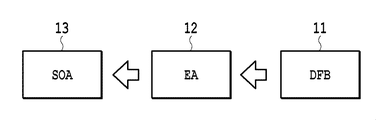
- FIG. 2 is a schematic diagram of the configuration of the SOA integrated EA-DFB laser used in the present invention.
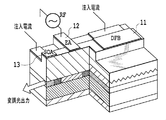
- FIG. 3A is a diagram illustrating the structure of the EA-DFB laser and the SOA integrated EA-DFB laser.
- FIG. 3B is a diagram illustrating the structure of the EA-DFB laser and the SOA integrated EA-DFB laser.
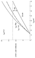
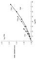
- FIG. 4 is a diagram showing measurement results of current injection amount-light output characteristics into the DFB laser unit in the EA-DFB laser and the SOA integrated EA-DFB laser.
- FIG. 5 is a diagram showing a gain calculation result of the SOA part in the SOA integrated EA-DFB laser.
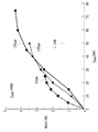
- FIG. 6 shows the measurement result of the light intensity gain for each SOA length L SOA in the SOA integrated EA-DFB laser.
- FIG. 7 is a diagram showing the measurement result of the power consumption of the SOA part of the SOA integrated EA-DFB laser.
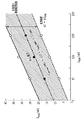
- FIG. 8 is a diagram showing a drive current range of the SOA unit 13 for each SOA length in the SOA integrated EA-DFB laser.
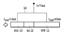
- FIG. 9 is a diagram for explaining an SOA integrated EA-DFB laser according to Embodiment 2 of the present invention.
- FIG. 2 is a schematic diagram of the configuration of the SOA integrated EA-DFB laser used in the present invention.
- the DFB laser unit 11, the EA modulator unit 12 that receives output light from the DFB laser unit 11, and the modulated output light that is modulated and output by the EA modulator unit 12 is input and amplified.
- An SOA integrated EA-DFB laser in which the SOA unit 13 is monolithically integrated on the same substrate is shown.
- FIG. 3A illustrates the structure of an EA-DFB laser
- FIG. 3B illustrates the structure of a SOA integrated EA-DFB laser used in the present invention.
- the EA-DFB laser (hereinafter simply referred to as “EA-DFB laser”) that is not integrated with the SOA described below has the same characteristics as the SOA integrated EA-DFB laser except that the SOA is not integrated. It shall have.
- the SOA integrated EA-DFB laser from the maximum permissible current (for example, 80 mA) to the DFB laser unit allowed when the EA-DFB laser is mounted on the optical transmission module, the SOA integrated EA-DFB laser
- the DFB injection current I DFB to the DFB laser unit 11 is reduced to a current (for example, 60 mA) that is larger than the threshold current of the DFB laser unit 11 and does not degrade the SMSR.
- a current that can realize power consumption is injected into the SOA unit 13.
- the power consumption P DFB in the DFB laser unit 11 is also reduced / reduced by reducing the DFB injection current I DFB to the DFB laser unit 11. Furthermore, as a result of the reduction of the input light intensity to the EA modulator unit 12, the photocurrent flowing through the EA modulator unit 12 is reduced, and the power consumption P EA in the EA modulator unit 12 is also reduced / reduced. In addition, by injecting current into the SOA unit 13 within the range of power that can be reduced by the DFB laser unit 11 and the EA modulator unit 12, it is possible to increase the light output of the entire laser and not increase the power consumption.
- the SOA injection current I SOA into the SOA unit 13 is as small as possible.
- an DFB that is allowed under the driving conditions of an optical transmission module equipped with an EA-DFB laser (that is, an optical transmission module that does not have an SOA or has an injection current I SOA into the SOA portion of 0).
- FIG. 4 shows measurement results of current injection amount-light output characteristics into the DFB laser part in the EA-DFB laser and the SOA integrated EA-DFB laser.
- the operating temperature is 45 ° C.
- the horizontal axis indicates the DFB injection current I DFB to the DFB laser unit 11.
- the DFB laser unit at a certain injection current I DFB the DFB laser unit at a certain injection current I DFB.
- FIG. 5 shows the gain calculation result of the SOA unit 13 in the SOA integrated EA-DFB laser.
- the gain calculation of the SOA unit 13 shown in FIG. 5 was performed using a rate equation, and the relationship between the input light intensity to the SOA unit 13, the SOA length L SOA, and the SOA injection current I SOA was examined.
- FIG. 6 shows the measurement result of the light intensity gain for each SOA length L SOA in the SOA integrated EA-DFB laser.
- FIG. 7 shows the measurement result of the power consumption of the SOA unit 13 of the SOA integrated EA-DFB laser.
- FIG. 8 shows the drive of the SOA unit 13 that can simultaneously achieve higher gain and lower power consumption than the conventional one while realizing a negative chirp value for each SOA length in the SOA integrated EA-DFB laser used in the present invention. Indicates the current range.
- the center drive current I center of the SOA part 13 of the EA-DFB laser was obtained.
- the upper and lower limits of the SOA injection current I SOA are defined from the viewpoint of power consumption and optical amplification as described above, DFB injection from the maximum allowable current to the DFB laser part of the EA-DFB laser measured and recorded in advance
- the reduction amount of the current I DFB is ⁇ I DFB
- the upper limit and the lower limit of the SOA injection current I SOA can be expressed as ⁇ ⁇ I DFB / 2 of the center drive current I center of the SOA unit 13.
- the current range ⁇ I DFB in which high output and low power consumption can be realized by SOA integration can be ⁇ 10 mA.
- the maximum allowable current to the DFB laser unit allowed when the EA-DFB laser is mounted on the optical transmission module is measured and recorded in advance.
- the reduction amount ⁇ I DFB is calculated from the difference between the maximum allowable current and the DFB injection current I DFB to the DFB laser unit 11 of the SOA integrated EA-DFB laser.
- I SOArng [mA] 115 [mA / mm] ⁇ L SOA [mm] +10 [mA] ⁇ ⁇ I DFB / 2 in the range of [mA] SOA injected current I SOA Is injected into the SOA unit 13.
- the SOA length of the SOA unit 13 in the optical waveguide direction is set to a range of 50 ⁇ m or more and 150 ⁇ m or less, the amount of current supplied to the DFB laser unit and the SOA unit, respectively, for each of the DFB laser unit and the SOA unit.
- Each driving condition can be satisfied, and a negative chirp value can be realized and an increase in power consumption of the DFB laser unit and the SOA unit can be further prevented. Therefore, it is preferable to set the SOA length L SOA of the SOA unit 13 in the range of 50 ⁇ m to 150 ⁇ m.
- Example 1 The SOA integrated EA-DFB laser according to Example 1 of the present invention will be described with reference to Table 1.
- Table 1 80mA drive current of EA-DFB laser, and 60mA injection current I DFB to DFB laser 12 in SOA integrated EA-DFB laser, SOA length L SOA is a 50 [mu] m, the operating temperature is 45 ° C.
- the characteristics of the EA-DFB laser and the SOA integrated EA-DFB laser when the injection current I SOA to the SOA unit 13 is driven at 10 mA or 25 mA are shown.
- P avg represents the light intensity
- DER represents the dynamic extinction ratio
- OMA represents the light modulation intensity
- f 3dB represents the cutoff frequency of the 3 dB band
- P represents the power consumption.
- I SOA 10 mA
- 25 mA is the drive current range of the SOA section 13
- Example 2 The SOA integrated EA-DFB laser according to the second embodiment of the present invention will be described with reference to FIG.
- the DFB laser unit 11, the EA modulator unit 12 that receives the output light from the DFB laser unit 11, and the modulated output light that is modulated by the EA modulator unit 12 is input and amplified.
- An SOA integrated EA-DFB laser in which the SOA unit 13 is monolithically integrated on the same substrate is shown.
- the DFB laser unit 11 and the SOA unit 13 are controlled using the same control terminal 14.
- the manufacturing process of the SOA integrated EA-DFB laser according to this example is disclosed in Patent Document 1, for example.
- the length of the SOA section 13 in the optical waveguide direction is 50 ⁇ m
- the SOA unit according to the present invention can achieve high output and power consumption.
- the ratio of the length of the SOA unit 13 and the DFB laser unit 11 so as to satisfy the drive current range I SOArng of 13, it is possible to simultaneously realize an increase in light intensity, a reduction in power consumption, and a negative chirp value. it can.
- the SOA integrated EA-DFB laser and the driving method thereof according to the present invention have been described above.
- the present invention is not limited to this.
- the gain of the SOA unit 13 may be calculated by other calculation methods.
Landscapes
- Physics & Mathematics (AREA)
- Condensed Matter Physics & Semiconductors (AREA)
- General Physics & Mathematics (AREA)
- Electromagnetism (AREA)
- Optics & Photonics (AREA)
- Semiconductor Lasers (AREA)
- Optical Modulation, Optical Deflection, Nonlinear Optics, Optical Demodulation, Optical Logic Elements (AREA)
Abstract
Description
PDFB=(IDFB-Ith)×ηdDFB
ΔPDFB=ΔIDFB×ηdDFB
表1を用いて、本発明の実施例1に係るSOA集積EA-DFBレーザを説明する。表1は、EA-DFBレーザの駆動電流を80mAとし、SOA集積EA-DFBレーザにおいてはDFBレーザ部12への注入電流IDFBを60mAとし、SOA長LSOAは50μmとし、動作温度は45℃とし、SOA部13への注入電流ISOAを10mA又は25mAで駆動した場合のEA-DFBレーザ及びSOA集積EA-DFBレーザの特性を示している。表1において、Pavgは光強度を示し、DERは動的消光比を示し、OMAは光変調強度を示し、f3dBは3dB帯域のカットオフ周波数を示し、Pは消費電力を示す。

図9を用いて、本発明の実施例2に係るSOA集積EA-DFBレーザを説明する。図9には、DFBレーザ部11と、DFBレーザ部11からの出力光を入力するEA変調器部12と、EA変調器部12において変調された出力された変調出力光を入力して増幅するSOA部13とが同一基板上にモノリシック集積されたSOA集積EA-DFBレーザが示されている。図9に示されるように、DFBレーザ部11及びSOA部13は、同一の制御端子14を用いて制御される。本実施例に係るSOA集積EA-DFBレーザの作製工程は、例えば特許文献1に示されている。
Claims (8)
- DFBレーザ部と、前記DFBレーザ部の後段に設けられたEA変調器部と、前記EA変調器部の後段に設けられたSOA部とが同一基板上にモノリシック集積されたSOA集積EA-DFBレーザの駆動方法であって、
EA-DFBレーザを光送信モジュールに搭載した場合に許容される前記EA-DFBレーザのDFBレーザ部への最大注入電流から削減量ΔIDFBを削減することによって前記SOA集積EA-DFBレーザのDFBレーザ部で削減できた消費電力と前記SOA集積EA-DFBレーザのEA変調器部で削減できた消費電力との合計分を超えない消費電力の範囲内で前記SOA部に電流ISOAを注入することを特徴とする駆動方法。 - 前記SOA部の光導波方向に関する長さをLSOAとすると、前記SOA部にISOA=115[mA/mm]×LSOA[mm]+10[mA]±ΔIDFB/2[mA]の範囲内で電流を注入して駆動することを特徴とする請求項1に記載の駆動方法。
- 前記SOA集積EA-DFBレーザのDFBレーザ部及びSOA部は同一の制御端子から電流を注入され、
ISOA=115[mA/mm]×LSOA[mm]+10[mA]±ΔIDFB/2[mA]を満たすように前記SOA集積EA-DFBレーザのDFBレーザ部及びSOA部の光導波方向に関する長さが設計されていることを特徴とする請求項1に記載の駆動方法。 - 前記SOA部の光導波方向に関する長さは、50μm以上150μm以下であることを特徴とする請求項1に記載の駆動方法。
- DFBレーザ部とEA変調器部とを含むEA-DFBレーザの出射端にSOA部が集積されたSOA集積EA-DFBレーザであって、
EA-DFBレーザを光送信モジュールに搭載した場合に許容される前記EA-DFBレーザのDFBレーザ部への最大注入電流から削減量ΔIDFBを削減することによって前記SOA集積EA-DFBレーザのDFBレーザ部で削減できた消費電力と前記SOA集積EA-DFBレーザのEA変調器部で削減できた消費電力との合計分を超えない消費電力の範囲内で前記SOA部に電流ISOAが注入されることを特徴とするSOA集積EA-DFBレーザ。 - 前記SOA部の光導波方向に関する長さをLSOAとすると、前記SOA部にISOA=115[mA/mm]×LSOA[mm]+10[mA]±ΔIDFB/2[mA]の範囲内で電流が注入されることを特徴とする請求項5に記載のSOA集積EA-DFBレーザ。
- 前記SOA集積EA-DFBレーザのDFBレーザ部及びSOA部は同一の制御端子から電流を注入され、
ISOA=115[mA/mm]×LSOA[mm]+10[mA]±ΔIDFB/2[mA]を満たすように前記SOA集積EA-DFBレーザのDFBレーザ部及びSOA部の光導波方向に関する長さが設計されていることを特徴とする請求項5に記載のSOA集積EA-DFBレーザ。 - 前記SOA部の光導波方向に関する長さは、50μm以上150μm以下であることを特徴とする請求項5のSOA集積EA-DFBレーザ。
Priority Applications (2)
| Application Number | Priority Date | Filing Date | Title |
|---|---|---|---|
| US15/547,886 US10128632B2 (en) | 2015-02-23 | 2016-02-16 | Electroabsorption modulator integrated distributed feedback laser with integrated semiconductor optical amplifier, and driving method for same |
| JP2017501897A JPWO2016136183A1 (ja) | 2015-02-23 | 2016-02-16 | Soa集積ea−dfbレーザ及びその駆動方法 |
Applications Claiming Priority (2)
| Application Number | Priority Date | Filing Date | Title |
|---|---|---|---|
| JP2015033309 | 2015-02-23 | ||
| JP2015-033309 | 2015-02-23 |
Publications (1)
| Publication Number | Publication Date |
|---|---|
| WO2016136183A1 true WO2016136183A1 (ja) | 2016-09-01 |
Family
ID=56789467
Family Applications (1)
| Application Number | Title | Priority Date | Filing Date |
|---|---|---|---|
| PCT/JP2016/000792 Ceased WO2016136183A1 (ja) | 2015-02-23 | 2016-02-16 | Soa集積ea-dfbレーザ及びその駆動方法 |
Country Status (3)
| Country | Link |
|---|---|
| US (1) | US10128632B2 (ja) |
| JP (1) | JPWO2016136183A1 (ja) |
| WO (1) | WO2016136183A1 (ja) |
Cited By (11)
| Publication number | Priority date | Publication date | Assignee | Title |
|---|---|---|---|---|
| JP2018060973A (ja) * | 2016-10-07 | 2018-04-12 | 日本電信電話株式会社 | 半導体光集積素子およびこれを搭載した光送受信モジュール |
| JP2018060974A (ja) * | 2016-10-07 | 2018-04-12 | 日本電信電話株式会社 | 半導体光集積素子 |
| JP2018060976A (ja) * | 2016-10-07 | 2018-04-12 | 日本電信電話株式会社 | 直接変調レーザ |
| JP2018060975A (ja) * | 2016-10-07 | 2018-04-12 | 日本電信電話株式会社 | 直接変調レーザ |
| JP2018060977A (ja) * | 2016-10-07 | 2018-04-12 | 日本電信電話株式会社 | 波長多重送信器 |
| JP2018073940A (ja) * | 2016-10-27 | 2018-05-10 | 住友電工デバイス・イノベーション株式会社 | 半導体レーザ装置の動作条件決定方法 |
| WO2019059066A1 (ja) * | 2017-09-19 | 2019-03-28 | 日本電信電話株式会社 | 半導体光集積素子 |
| WO2019102604A1 (ja) * | 2017-11-27 | 2019-05-31 | 三菱電機株式会社 | 半導体光送信器 |
| WO2019172089A1 (ja) * | 2018-03-07 | 2019-09-12 | 日本電信電話株式会社 | 半導体光集積素子およびその製造方法 |
| JP2019192918A (ja) * | 2019-05-27 | 2019-10-31 | 三菱電機株式会社 | 半導体光集積素子 |
| JP2024091613A (ja) * | 2022-12-23 | 2024-07-04 | 三菱電機株式会社 | 光モジュール |
Families Citing this family (8)
| Publication number | Priority date | Publication date | Assignee | Title |
|---|---|---|---|---|
| CN108879321A (zh) * | 2018-09-12 | 2018-11-23 | 成都微泰光芯技术有限公司 | 一种集成soa的eml芯片 |
| JP7147611B2 (ja) * | 2019-02-12 | 2022-10-05 | 日本電信電話株式会社 | 高出力直接変調型レーザ |
| US12316074B2 (en) * | 2019-09-26 | 2025-05-27 | Nippon Telegraph And Telephone Corporation | Optical transmitter |
| WO2022003925A1 (ja) * | 2020-07-02 | 2022-01-06 | 日本電信電話株式会社 | 光送信器 |
| US11705692B2 (en) * | 2020-07-28 | 2023-07-18 | Cisco Technology, Inc. | Laser side mode suppression ratio control |
| DE102020125719A1 (de) * | 2020-10-01 | 2022-04-07 | OSRAM Opto Semiconductors Gesellschaft mit beschränkter Haftung | Bauteil mit strukturierter anschlussfläche und verfahren zum betreiben eines bauteils |
| WO2022107311A1 (ja) * | 2020-11-20 | 2022-05-27 | 日本電信電話株式会社 | 光送信器 |
| US20220255295A1 (en) * | 2021-02-05 | 2022-08-11 | Inphi Corporation | High-power tunable laser on silicon photonics platform |
Citations (5)
| Publication number | Priority date | Publication date | Assignee | Title |
|---|---|---|---|---|
| JPH05291694A (ja) * | 1992-04-07 | 1993-11-05 | Hitachi Ltd | 低チャープ光源 |
| JPH06181366A (ja) * | 1992-12-14 | 1994-06-28 | Fujitsu Ltd | 光半導体装置 |
| US20050006654A1 (en) * | 2003-07-08 | 2005-01-13 | Byung-Kwon Kang | Semiconductor monolithic integrated optical transmitter |
| JP2013258337A (ja) * | 2012-06-13 | 2013-12-26 | Nippon Telegr & Teleph Corp <Ntt> | 半導体光集積素子 |
| JP2013258336A (ja) * | 2012-06-13 | 2013-12-26 | Nippon Telegr & Teleph Corp <Ntt> | 半導体光集積素子 |
Family Cites Families (5)
| Publication number | Priority date | Publication date | Assignee | Title |
|---|---|---|---|---|
| EP0984534B1 (en) * | 1994-03-18 | 2003-06-04 | Fujitsu Limited | Drive circuit of a semiconductor optical modulator |
| JP2001144367A (ja) * | 1999-11-11 | 2001-05-25 | Mitsubishi Electric Corp | 半導体レーザ装置及びその駆動方法 |
| EP1436870A2 (en) * | 2001-10-09 | 2004-07-14 | Infinera Corporation | TRANSMITTER PHOTONIC INTEGRATED CIRCUITS (TxPIC) AND OPTICAL TRANSPORT NETWORKS EMPLOYING TxPICs |
| EP1436931B1 (en) * | 2001-10-09 | 2005-12-28 | Infinera Corporation | Digital optical network architecture |
| SE520139C2 (sv) * | 2001-11-30 | 2003-06-03 | Optillion Ab | Lasermodulator med elektriskt separerade laser- och modulatorsektioner |
-
2016
- 2016-02-16 US US15/547,886 patent/US10128632B2/en active Active
- 2016-02-16 WO PCT/JP2016/000792 patent/WO2016136183A1/ja not_active Ceased
- 2016-02-16 JP JP2017501897A patent/JPWO2016136183A1/ja active Pending
Patent Citations (5)
| Publication number | Priority date | Publication date | Assignee | Title |
|---|---|---|---|---|
| JPH05291694A (ja) * | 1992-04-07 | 1993-11-05 | Hitachi Ltd | 低チャープ光源 |
| JPH06181366A (ja) * | 1992-12-14 | 1994-06-28 | Fujitsu Ltd | 光半導体装置 |
| US20050006654A1 (en) * | 2003-07-08 | 2005-01-13 | Byung-Kwon Kang | Semiconductor monolithic integrated optical transmitter |
| JP2013258337A (ja) * | 2012-06-13 | 2013-12-26 | Nippon Telegr & Teleph Corp <Ntt> | 半導体光集積素子 |
| JP2013258336A (ja) * | 2012-06-13 | 2013-12-26 | Nippon Telegr & Teleph Corp <Ntt> | 半導体光集積素子 |
Cited By (15)
| Publication number | Priority date | Publication date | Assignee | Title |
|---|---|---|---|---|
| JP2018060973A (ja) * | 2016-10-07 | 2018-04-12 | 日本電信電話株式会社 | 半導体光集積素子およびこれを搭載した光送受信モジュール |
| JP2018060974A (ja) * | 2016-10-07 | 2018-04-12 | 日本電信電話株式会社 | 半導体光集積素子 |
| JP2018060976A (ja) * | 2016-10-07 | 2018-04-12 | 日本電信電話株式会社 | 直接変調レーザ |
| JP2018060975A (ja) * | 2016-10-07 | 2018-04-12 | 日本電信電話株式会社 | 直接変調レーザ |
| JP2018060977A (ja) * | 2016-10-07 | 2018-04-12 | 日本電信電話株式会社 | 波長多重送信器 |
| JP2018073940A (ja) * | 2016-10-27 | 2018-05-10 | 住友電工デバイス・イノベーション株式会社 | 半導体レーザ装置の動作条件決定方法 |
| WO2019059066A1 (ja) * | 2017-09-19 | 2019-03-28 | 日本電信電話株式会社 | 半導体光集積素子 |
| JPWO2019059066A1 (ja) * | 2017-09-19 | 2020-01-16 | 日本電信電話株式会社 | 半導体光集積素子 |
| WO2019102604A1 (ja) * | 2017-11-27 | 2019-05-31 | 三菱電機株式会社 | 半導体光送信器 |
| JPWO2019102604A1 (ja) * | 2017-11-27 | 2019-12-12 | 三菱電機株式会社 | 半導体光送信器 |
| WO2019172089A1 (ja) * | 2018-03-07 | 2019-09-12 | 日本電信電話株式会社 | 半導体光集積素子およびその製造方法 |
| JP2019160840A (ja) * | 2018-03-07 | 2019-09-19 | 日本電信電話株式会社 | 半導体光集積素子およびその製造方法 |
| JP2019192918A (ja) * | 2019-05-27 | 2019-10-31 | 三菱電機株式会社 | 半導体光集積素子 |
| JP2024091613A (ja) * | 2022-12-23 | 2024-07-04 | 三菱電機株式会社 | 光モジュール |
| JP7734768B2 (ja) | 2022-12-23 | 2025-09-05 | 三菱電機株式会社 | 光モジュール |
Also Published As
| Publication number | Publication date |
|---|---|
| US10128632B2 (en) | 2018-11-13 |
| JPWO2016136183A1 (ja) | 2017-07-20 |
| US20180026424A1 (en) | 2018-01-25 |
Similar Documents
| Publication | Publication Date | Title |
|---|---|---|
| JPWO2016136183A1 (ja) | Soa集積ea−dfbレーザ及びその駆動方法 | |
| Ramdane et al. | Monolithic integration of multiple-quantum-well lasers and modulators for high-speed transmission | |
| US9059801B1 (en) | Optical modulator | |
| Aoki et al. | High-speed (10 Gbit/s) and low-drive-voltage (1 V peak to peak) InGaAs/InGaAsP MQW electroabsorption-modulator integrated DFB laser with semi-insulating buried heterostructure | |
| US9564733B2 (en) | Method of fabricating and operating an optical modulator | |
| JPWO2017135381A1 (ja) | 光送信器及び光強度モニタ方法 | |
| Otsubo et al. | 1.3-$\mu $ m AlGaInAs Multiple-Quantum-Well Semi-insulating Buried-Heterostructure Distributed-Feedback Lasers for High-Speed Direct Modulation | |
| Simoyama et al. | 50-Gbps direct modulation using 1.3-μm AlGaInAs MQW distribute-reflector lasers | |
| JP2013168500A (ja) | 光半導体装置 | |
| CN104617486B (zh) | 单片集成式多波长半导体锁模激光器 | |
| JP4421951B2 (ja) | 光送信モジュール | |
| JP2017118052A (ja) | 波長多重光送信器及びその制御方法 | |
| Dubrovina et al. | Record high power 13dBm electro-absorption modulated laser for 50G-PON | |
| JP6454256B2 (ja) | 波長多重光送信器 | |
| Cao et al. | A novel bidirectionally operated chirped quantum-dot based semiconductor optical amplifier using a dual ground state spectrum | |
| JP7343807B2 (ja) | 光送信器 | |
| JP2019004093A (ja) | 半導体光集積装置 | |
| JP7077549B2 (ja) | 多波長光源 | |
| US8130443B2 (en) | Optical waveform reshaping device | |
| Debrégeas et al. | Extremely high-power laser-modulators with integrated amplifier section (EML-SOAs) | |
| CN118199735A (zh) | 基于半导体光放大器的光传输方法及其装置 | |
| Chen et al. | Efficient, high power, low chirp electro-absorption modulated laser integrated with SOA for 50G PON application | |
| WO2019102604A1 (ja) | 半導体光送信器 | |
| CN118137282A (zh) | 激光调制装置及发射机 | |
| JP2018093443A (ja) | 光半導体送信器 |
Legal Events
| Date | Code | Title | Description |
|---|---|---|---|
| 121 | Ep: the epo has been informed by wipo that ep was designated in this application |
Ref document number: 16754936 Country of ref document: EP Kind code of ref document: A1 |
|
| ENP | Entry into the national phase |
Ref document number: 2017501897 Country of ref document: JP Kind code of ref document: A |
|
| WWE | Wipo information: entry into national phase |
Ref document number: 15547886 Country of ref document: US |
|
| NENP | Non-entry into the national phase |
Ref country code: DE |
|
| 122 | Ep: pct application non-entry in european phase |
Ref document number: 16754936 Country of ref document: EP Kind code of ref document: A1 |