WO2016133103A1 - 走査露光装置 - Google Patents
走査露光装置 Download PDFInfo
- Publication number
- WO2016133103A1 WO2016133103A1 PCT/JP2016/054518 JP2016054518W WO2016133103A1 WO 2016133103 A1 WO2016133103 A1 WO 2016133103A1 JP 2016054518 W JP2016054518 W JP 2016054518W WO 2016133103 A1 WO2016133103 A1 WO 2016133103A1
- Authority
- WO
- WIPO (PCT)
- Prior art keywords
- stage
- substrate
- light
- light source
- scanning
- Prior art date
- Legal status (The legal status is an assumption and is not a legal conclusion. Google has not performed a legal analysis and makes no representation as to the accuracy of the status listed.)
- Ceased
Links
Images



Classifications
-
- G—PHYSICS
- G03—PHOTOGRAPHY; CINEMATOGRAPHY; ANALOGOUS TECHNIQUES USING WAVES OTHER THAN OPTICAL WAVES; ELECTROGRAPHY; HOLOGRAPHY
- G03F—PHOTOMECHANICAL PRODUCTION OF TEXTURED OR PATTERNED SURFACES, e.g. FOR PRINTING, FOR PROCESSING OF SEMICONDUCTOR DEVICES; MATERIALS THEREFOR; ORIGINALS THEREFOR; APPARATUS SPECIALLY ADAPTED THEREFOR
- G03F7/00—Photomechanical, e.g. photolithographic, production of textured or patterned surfaces, e.g. printing surfaces; Materials therefor, e.g. comprising photoresists; Apparatus specially adapted therefor
- G03F7/20—Exposure; Apparatus therefor
- G03F7/2002—Exposure; Apparatus therefor with visible light or UV light, through an original having an opaque pattern on a transparent support, e.g. film printing, projection printing; by reflection of visible or UV light from an original such as a printed image
- G03F7/2004—Exposure; Apparatus therefor with visible light or UV light, through an original having an opaque pattern on a transparent support, e.g. film printing, projection printing; by reflection of visible or UV light from an original such as a printed image characterised by the use of a particular light source, e.g. fluorescent lamps or deep UV light
-
- H—ELECTRICITY
- H04—ELECTRIC COMMUNICATION TECHNIQUE
- H04N—PICTORIAL COMMUNICATION, e.g. TELEVISION
- H04N1/00—Scanning, transmission or reproduction of documents or the like, e.g. facsimile transmission; Details thereof
- H04N1/024—Details of scanning heads ; Means for illuminating the original
- H04N1/028—Details of scanning heads ; Means for illuminating the original for picture information pick-up
- H04N1/02815—Means for illuminating the original, not specific to a particular type of pick-up head
- H04N1/0282—Using a single or a few point light sources, e.g. a laser diode
-
- G—PHYSICS
- G03—PHOTOGRAPHY; CINEMATOGRAPHY; ANALOGOUS TECHNIQUES USING WAVES OTHER THAN OPTICAL WAVES; ELECTROGRAPHY; HOLOGRAPHY
- G03F—PHOTOMECHANICAL PRODUCTION OF TEXTURED OR PATTERNED SURFACES, e.g. FOR PRINTING, FOR PROCESSING OF SEMICONDUCTOR DEVICES; MATERIALS THEREFOR; ORIGINALS THEREFOR; APPARATUS SPECIALLY ADAPTED THEREFOR
- G03F1/00—Originals for photomechanical production of textured or patterned surfaces, e.g., masks, photo-masks, reticles; Mask blanks or pellicles therefor; Containers specially adapted therefor; Preparation thereof
- G03F1/88—Originals for photomechanical production of textured or patterned surfaces, e.g., masks, photo-masks, reticles; Mask blanks or pellicles therefor; Containers specially adapted therefor; Preparation thereof prepared by photographic processes for production of originals simulating relief
-
- G—PHYSICS
- G03—PHOTOGRAPHY; CINEMATOGRAPHY; ANALOGOUS TECHNIQUES USING WAVES OTHER THAN OPTICAL WAVES; ELECTROGRAPHY; HOLOGRAPHY
- G03F—PHOTOMECHANICAL PRODUCTION OF TEXTURED OR PATTERNED SURFACES, e.g. FOR PRINTING, FOR PROCESSING OF SEMICONDUCTOR DEVICES; MATERIALS THEREFOR; ORIGINALS THEREFOR; APPARATUS SPECIALLY ADAPTED THEREFOR
- G03F7/00—Photomechanical, e.g. photolithographic, production of textured or patterned surfaces, e.g. printing surfaces; Materials therefor, e.g. comprising photoresists; Apparatus specially adapted therefor
- G03F7/20—Exposure; Apparatus therefor
- G03F7/2051—Exposure without an original mask, e.g. using a programmed deflection of a point source, by scanning, by drawing with a light beam, using an addressed light or corpuscular source
- G03F7/2059—Exposure without an original mask, e.g. using a programmed deflection of a point source, by scanning, by drawing with a light beam, using an addressed light or corpuscular source using a scanning corpuscular radiation beam, e.g. an electron beam
-
- G—PHYSICS
- G03—PHOTOGRAPHY; CINEMATOGRAPHY; ANALOGOUS TECHNIQUES USING WAVES OTHER THAN OPTICAL WAVES; ELECTROGRAPHY; HOLOGRAPHY
- G03F—PHOTOMECHANICAL PRODUCTION OF TEXTURED OR PATTERNED SURFACES, e.g. FOR PRINTING, FOR PROCESSING OF SEMICONDUCTOR DEVICES; MATERIALS THEREFOR; ORIGINALS THEREFOR; APPARATUS SPECIALLY ADAPTED THEREFOR
- G03F7/00—Photomechanical, e.g. photolithographic, production of textured or patterned surfaces, e.g. printing surfaces; Materials therefor, e.g. comprising photoresists; Apparatus specially adapted therefor
- G03F7/70—Microphotolithographic exposure; Apparatus therefor
- G03F7/70691—Handling of masks or workpieces
- G03F7/70716—Stages
-
- H—ELECTRICITY
- H04—ELECTRIC COMMUNICATION TECHNIQUE
- H04N—PICTORIAL COMMUNICATION, e.g. TELEVISION
- H04N1/00—Scanning, transmission or reproduction of documents or the like, e.g. facsimile transmission; Details thereof
- H04N1/40—Picture signal circuits
- H04N1/40056—Circuits for driving or energising particular reading heads or original illumination means
-
- H—ELECTRICITY
- H04—ELECTRIC COMMUNICATION TECHNIQUE
- H04N—PICTORIAL COMMUNICATION, e.g. TELEVISION
- H04N1/00—Scanning, transmission or reproduction of documents or the like, e.g. facsimile transmission; Details thereof
- H04N1/40—Picture signal circuits
- H04N1/401—Compensating positionally unequal response of the pick-up or reproducing head
Definitions
- the present invention relates to a scanning exposure apparatus.
- a scanning exposure apparatus is an apparatus that exposes a substrate while relatively moving a light source unit and a stage that supports the substrate, and exposes a mask pattern (see Patent Document 1 below) or exposure for photo-alignment (Patent Document below). 2).
- the scanning exposure apparatus includes a light source unit extending along one direction of the substrate plane, a direction intersecting the extending direction of the light source unit is defined as a scanning direction, and a light irradiation region of the light source unit is defined along the scanning direction.
- a uniform exposure is performed on a relatively large substrate by moving the substrate relative to the light irradiation region while realizing uniform exposure in the limited area.
- the illuminance of the light source and the scanning speed are increased in order to improve the tact time of the exposure process (or improve the throughput).
- the light source is turned on in advance before the substrate enters the light irradiation region.
- the substrate supported on the stage is provided with a gap between the stage surface and the substrate by pin support or the like in order to avoid the influence of static electricity on the stage surface.
- the present invention is an example of a problem to deal with such a problem.
- the illuminance of the light source is increased and the scanning speed is increased, it is possible to prevent exposure unevenness from occurring near the edge of the substrate. Is the object of the present invention.
- a scanning exposure apparatus comprises the following arrangement.
- a stage that supports the substrate by providing a gap between the surface of the stage, a light source unit that irradiates light to a light irradiation region that extends along one direction on the substrate, and one of the stage and the light source unit Or a scanning device that relatively moves both along a scanning direction that intersects the one direction, and the scanning device moves the stage and the light source unit from a position where the stage and the light source unit are stationary to the light irradiation region.
- the scanning exposure apparatus is characterized in that an acceleration section is provided until a substrate supported by the substrate enters, and the stage includes a light-shielding body that covers a gap between the stage surface and the substrate at an end of the stage. .
- the scanning exposure apparatus of the present invention having such a feature is provided with a light shielding provided at the end of the stage, even if the light emitted from the light source unit becomes stray light and enters the gap between the stage surface and the substrate in the acceleration section. Since the body shields this, it is possible to avoid a phenomenon in which the edge of the substrate is exposed from the back side of the substrate. As a result, the occurrence of uneven exposure near the edge of the substrate can be prevented, and uniform scanning exposure can be realized over the entire surface of the substrate.
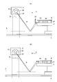
- FIG. 1 is an explanatory diagram showing functions of a scanning exposure apparatus according to an embodiment of the present invention ((a) is an explanatory diagram showing functions of the present invention, and (b) is an explanatory diagram showing problems of the prior art). It is explanatory drawing which showed an example of the light source unit of the scanning exposure apparatus which concerns on embodiment of this invention.
- FIG. 1 shows a scanning exposure apparatus according to an embodiment of the present invention ((a) is an explanatory view in side view, and (b) is an explanatory view in plan view).
- the scanning exposure apparatus 1 includes a stage 2, a light source unit 3, and a scanning device 4.
- the orthogonal directions in the plane along the substrate W are defined as the X and Y directions, and the direction orthogonal to the plane along the substrate W is defined as the Z direction.
- the stage 2 supports the substrate W by providing a gap 2S between the stage surface 2A.
- the gap 2S is formed by supporting the substrate W on the upper end of the pin 2P standing on the stage surface 2A.
- the present invention is not limited to this.
- the gap 2S is formed by air support or the like. May be.
- the light source unit 3 irradiates light to a light irradiation region 3L extending along one direction (X direction in the drawing) on the substrate W.
- a light source 30, a reflection member 31 that reflects light emitted from the light source 30, and a polarizing plate 32 such as a wire grid are provided.
- the light irradiation region 3L extends in the X direction and has a width L limited to the Y direction.
- the scanning device 4 relatively moves one or both of the stage 2 and the light source unit 3 along a scanning direction S (Y direction in the drawing) intersecting one direction (X direction).
- a scanning direction S (Y direction in the drawing) intersecting one direction (X direction).
- the light source unit 3 is fixed and the stage 2 is moved along the scanning direction S.
- the stage 2 is fixed and the light source unit 3 is moved along the scanning direction S. It may be moved.
- the scanning device 4 is provided with an acceleration section F from the position where the stage 2 and the light source unit 3 are stationary until the substrate W supported by the stage 2 enters the light irradiation region 3L.
- This acceleration section F is necessary to obtain a constant scanning speed from the time when one end of the substrate W in the Y direction enters the light irradiation region 3L until the other end of the substrate W in the Y direction exits from the light irradiation region 3L. Since there is a limit to increasing the acceleration, if the scanning speed is set high, the acceleration section F must be set longer.
- the stage 2 is provided with a light shielding body 20 covering the gap 2S between the stage surface 2A and the substrate W at the end of the stage 2.
- the light shielding bodies 20 are provided at both ends of the stage 2 that intersect the scanning direction S. However, of the both ends that intersect the scanning direction S, only the end on the side that enters the light irradiation region 3L.
- a light shield 20 may be provided. Further, the light shielding body 20 may be provided at the end of the stage 2 along the scanning direction S so that the entire circumference of the stage 2 is surrounded by the light shielding body 20.
- FIG. 2 shows an operation example of the scanning exposure apparatus 1 when scanning exposure is performed by moving the stage 2 (with the light source unit 3 stationary).
- the substrate W is carried into the stage 2 at a position away from the light irradiation region 3L of the light source unit 3 only in the acceleration section F, and the scanning speed (stage moving speed) while moving the stage 2 only in the acceleration section F. Is increased to the set speed Sa.
- the moving distance (L + W1) until the entire substrate W having the length W1 along the scanning direction S passes through the light irradiation region 3L having the width L.
- a constant scanning speed is maintained, and during that time, uniform scanning exposure is performed on the substrate W.
- the stage 2 is stopped when the substrate W is separated from the light irradiation region 3L by the acceleration section F, and the substrate W is unloaded.
- the light source 30 of the light source unit 3 since the light source 30 of the light source unit 3 is already lit while the stage 2 is moving in the acceleration section F, the light emitted from the light source 30 is reflected by the floor surface 5 and the stray light R is generated. The light is irradiated toward the substrate W. At this time, if the light blocking body 20 as in the embodiment of the present invention is not provided, the stray light R enters the gap 2S between the stage surface 2A and the substrate W as shown in FIG. Occurs from the back side. Further, the light emitted from the light source 30 is reflected by the floor surface 5 and the like, passes through the vicinity of the end of the substrate W, and is multiple-reflected by structures around the stage 2, and the substrate W is reflected from above the substrate W.
- the phenomenon of exposure occurs. When such a phenomenon occurs, unnecessary additional exposure is performed near the edge of the substrate W or near the center of the substrate W, and no matter how uniform the exposure in the regular light irradiation region 3L is, the upper surface of the substrate W is exposed. Therefore, uneven exposure occurs partially.
- a light shield 20 is provided at the end of the stage 2, and the light shield 20 provides a gap 2 ⁇ / b> S between the stage surface 2 ⁇ / b> A and the substrate W. Since it is covered, even when stray light R as shown in the figure is generated, it can be prevented from entering the gap 2S. Further, stray light that passes through the vicinity of the end of the substrate W and is subjected to multiple reflections by structures around the stage 2 to expose the substrate W from above the substrate W can be prevented. Thereby, the exposure of the substrate W is limited to only the scanning exposure within the regular light irradiation region 3L, and the above-described exposure unevenness can be avoided.
- Such a scanning exposure apparatus 1 can be used for a photo-alignment process in which the light source unit 3 irradiates ultraviolet rays and a photo-alignment material layer is formed on the substrate W, and an effective uniform alignment film on the substrate W. Can be formed. That is, by providing the light shielding body 20 at the end of the stage 2, the reaction of the photo-alignment material layer before the substrate W enters the light irradiation region 3L can be suppressed, so that the light source unit 3 is not changed. This makes it possible to apply more sensitive materials. Further, not only the acceleration section F but also a partial reaction when the substrate W is carried onto the stage 2 can be suppressed.
- the acceleration section F can be increased while realizing uniform exposure, the illuminance of the light source unit 3 can be increased and exposure can be performed at a higher scanning speed.
- the tact time can be improved and the throughput can be improved.
- the light source unit 3 is continuously turned on and the plurality of substrates W are successively exposed with stable emitted light, uniform exposure can be performed on each substrate W, and at that time, it is necessary to provide a light source shutter. Since there is no problem, problems such as particle generation due to opening and closing of the shutter and thermal deformation of the light source shutter itself do not occur.
- the light source unit 3 only needs to irradiate light onto the light irradiation region 3L extending along one direction on the substrate W (direction intersecting the scanning direction S).
- the light irradiation region 3 ⁇ / b> L is formed by arranging a plurality of light sources 30 ⁇ / b> A extending along the scanning direction S in the direction intersecting the scanning direction S, as shown in FIG. 4. You may do.
Landscapes
- Physics & Mathematics (AREA)
- Engineering & Computer Science (AREA)
- Multimedia (AREA)
- Signal Processing (AREA)
- General Physics & Mathematics (AREA)
- Optics & Photonics (AREA)
- Health & Medical Sciences (AREA)
- Toxicology (AREA)
- Exposure And Positioning Against Photoresist Photosensitive Materials (AREA)
- Liquid Crystal (AREA)
Abstract
Description
ステージ表面との間に間隙を設けて基板を支持するステージと、前記基板上の一方向に沿って延設される光照射領域に光を照射する光源ユニットと、前記ステージと前記光源ユニットの一方又は両方を、前記一方向に交差する走査方向に沿って相対的に移動させる走査装置とを備え、前記走査装置には、前記ステージ及び前記光源ユニットが静止した位置から前記光照射領域に前記ステージに支持された基板が入るまでの加速区間が設けられ、前記ステージは、前記ステージ表面と前記基板との間の間隙を覆う遮光体を当該ステージの端部に備えることを特徴とする走査露光装置。
2S:間隙,20:遮光体,
3:光源ユニット,3L:光照射領域,
30,30A:光源,31:反射部材,32:偏光板,
4:走査装置,5:床面,
S:走査方向,W:基板,R:迷光
Claims (4)
- ステージ表面との間に間隙を設けて基板を支持するステージと、
前記基板上の一方向に沿って延設される光照射領域に光を照射する光源ユニットと、
前記ステージと前記光源ユニットの一方又は両方を、前記一方向に交差する走査方向に沿って相対的に移動させる走査装置とを備え、
前記走査装置には、前記ステージ及び前記光源ユニットが静止した位置から前記光照射領域に前記ステージに支持された基板が入るまでの加速区間が設けられ、
前記ステージは、前記ステージ表面と前記基板との間の間隙を覆う遮光体を当該ステージの端部に備えることを特徴とする走査露光装置。 - 前記ステージは、前記ステージ表面に立設された複数のピンの上端で前記基板を支持することを特徴とする請求項1記載の走査露光装置。
- 前記光源ユニットは紫外線を照射することを特徴とする請求項1又は2記載の走査露光装置。
- 前記基板上には、光配向材料層が形成されていることを特徴とする請求項3記載の走査露光装置。
Priority Applications (4)
| Application Number | Priority Date | Filing Date | Title |
|---|---|---|---|
| US15/551,378 US10469692B2 (en) | 2015-02-18 | 2016-02-17 | Scanning exposure device |
| KR1020177022388A KR20170117071A (ko) | 2015-02-18 | 2016-02-17 | 주사 노광 장치 |
| JP2017500698A JP6712587B2 (ja) | 2015-02-18 | 2016-02-17 | 走査露光装置 |
| CN201680010209.3A CN107407888B (zh) | 2015-02-18 | 2016-02-17 | 扫描曝光装置 |
Applications Claiming Priority (2)
| Application Number | Priority Date | Filing Date | Title |
|---|---|---|---|
| JP2015-030025 | 2015-02-18 | ||
| JP2015030025 | 2015-02-18 |
Publications (1)
| Publication Number | Publication Date |
|---|---|
| WO2016133103A1 true WO2016133103A1 (ja) | 2016-08-25 |
Family
ID=56692263
Family Applications (1)
| Application Number | Title | Priority Date | Filing Date |
|---|---|---|---|
| PCT/JP2016/054518 Ceased WO2016133103A1 (ja) | 2015-02-18 | 2016-02-17 | 走査露光装置 |
Country Status (6)
| Country | Link |
|---|---|
| US (1) | US10469692B2 (ja) |
| JP (1) | JP6712587B2 (ja) |
| KR (1) | KR20170117071A (ja) |
| CN (1) | CN107407888B (ja) |
| TW (1) | TWI698714B (ja) |
| WO (1) | WO2016133103A1 (ja) |
Cited By (1)
| Publication number | Priority date | Publication date | Assignee | Title |
|---|---|---|---|---|
| WO2019031453A1 (ja) * | 2017-08-09 | 2019-02-14 | 株式会社ブイ・テクノロジー | 光配向用露光装置 |
Citations (4)
| Publication number | Priority date | Publication date | Assignee | Title |
|---|---|---|---|---|
| JP2005150708A (ja) * | 2003-10-24 | 2005-06-09 | Nikon Corp | 静電チャック、ステージ装置及び露光装置 |
| JP2008010643A (ja) * | 2006-06-29 | 2008-01-17 | Canon Inc | ステージ装置 |
| JP2009075303A (ja) * | 2007-09-20 | 2009-04-09 | Seiko Epson Corp | 電気光学装置の製造装置及び製造方法 |
| JP2014174287A (ja) * | 2013-03-07 | 2014-09-22 | V Technology Co Ltd | 走査露光装置及び走査露光方法 |
Family Cites Families (9)
| Publication number | Priority date | Publication date | Assignee | Title |
|---|---|---|---|---|
| JPH0758423A (ja) * | 1993-08-19 | 1995-03-03 | Sony Corp | バックアップピン受け部を設けたプリント基板 |
| JP2002151400A (ja) * | 2000-11-15 | 2002-05-24 | Canon Inc | 露光装置、その保守方法並びに同装置を用いた半導体デバイス製造方法及び半導体製造工場 |
| JP2009295950A (ja) | 2008-05-09 | 2009-12-17 | Nsk Ltd | スキャン露光装置およびスキャン露光方法 |
| JP5294488B2 (ja) * | 2009-12-03 | 2013-09-18 | 株式会社ブイ・テクノロジー | 露光装置 |
| CN103365123B (zh) * | 2012-04-06 | 2015-08-26 | 上海微电子装备有限公司 | 一种对准系统光阑板的调整机构 |
| JP6239813B2 (ja) * | 2012-07-18 | 2017-11-29 | 株式会社Screenセミコンダクターソリューションズ | 基板処理装置および基板処理方法 |
| JP5344105B1 (ja) * | 2013-03-08 | 2013-11-20 | ウシオ電機株式会社 | 光配向用偏光光照射装置及び光配向用偏光光照射方法 |
| US20190086697A1 (en) * | 2016-05-27 | 2019-03-21 | Sharp Kabushiki Kaisha | Method for manufacturing liquid crystal display device |
| JP6985803B2 (ja) * | 2017-03-01 | 2021-12-22 | 株式会社Screenホールディングス | 露光装置、基板処理装置、基板の露光方法および基板処理方法 |
-
2016
- 2016-02-17 TW TW105104656A patent/TWI698714B/zh not_active IP Right Cessation
- 2016-02-17 JP JP2017500698A patent/JP6712587B2/ja not_active Expired - Fee Related
- 2016-02-17 US US15/551,378 patent/US10469692B2/en not_active Expired - Fee Related
- 2016-02-17 KR KR1020177022388A patent/KR20170117071A/ko not_active Ceased
- 2016-02-17 CN CN201680010209.3A patent/CN107407888B/zh not_active Expired - Fee Related
- 2016-02-17 WO PCT/JP2016/054518 patent/WO2016133103A1/ja not_active Ceased
Patent Citations (4)
| Publication number | Priority date | Publication date | Assignee | Title |
|---|---|---|---|---|
| JP2005150708A (ja) * | 2003-10-24 | 2005-06-09 | Nikon Corp | 静電チャック、ステージ装置及び露光装置 |
| JP2008010643A (ja) * | 2006-06-29 | 2008-01-17 | Canon Inc | ステージ装置 |
| JP2009075303A (ja) * | 2007-09-20 | 2009-04-09 | Seiko Epson Corp | 電気光学装置の製造装置及び製造方法 |
| JP2014174287A (ja) * | 2013-03-07 | 2014-09-22 | V Technology Co Ltd | 走査露光装置及び走査露光方法 |
Cited By (1)
| Publication number | Priority date | Publication date | Assignee | Title |
|---|---|---|---|---|
| WO2019031453A1 (ja) * | 2017-08-09 | 2019-02-14 | 株式会社ブイ・テクノロジー | 光配向用露光装置 |
Also Published As
| Publication number | Publication date |
|---|---|
| KR20170117071A (ko) | 2017-10-20 |
| US20180041656A1 (en) | 2018-02-08 |
| TW201643550A (zh) | 2016-12-16 |
| JP6712587B2 (ja) | 2020-06-24 |
| US10469692B2 (en) | 2019-11-05 |
| TWI698714B (zh) | 2020-07-11 |
| CN107407888B (zh) | 2019-03-29 |
| JPWO2016133103A1 (ja) | 2018-02-15 |
| CN107407888A (zh) | 2017-11-28 |
Similar Documents
| Publication | Publication Date | Title |
|---|---|---|
| KR102171301B1 (ko) | Dmd를 이용한 디지털 노광기 및 그 제어 방법 | |
| JP2011233781A5 (ja) | ||
| TWI463270B (zh) | 雷射曝光裝置 | |
| KR102272435B1 (ko) | 편광광 조사장치 | |
| JP6078843B2 (ja) | 光配向露光方法及び光配向露光装置 | |
| JP2013094737A (ja) | 紫外線照射装置 | |
| KR102269979B1 (ko) | 묘화 장치, 및 묘화 방법 | |
| JP2013191628A5 (ja) | ||
| JP6712587B2 (ja) | 走査露光装置 | |
| CN103257530A (zh) | 接近式曝光装置、曝光光形成方法、面板基板的制造方法 | |
| JP6002261B2 (ja) | 光照射装置 | |
| CN101799632B (zh) | 光照射装置 | |
| JP5501201B2 (ja) | 周辺露光装置及びその方法 | |
| JP6500543B2 (ja) | 偏光子、光配向装置、および光配向方法 | |
| JP7007963B2 (ja) | 光照射装置 | |
| WO2017068962A1 (ja) | 光照射装置 | |
| JP2011119419A (ja) | レーザ処理装置及びレーザ処理方法 | |
| JP2008233616A (ja) | 周辺露光装置およびパネル構造物の製造方法 | |
| JP7191434B2 (ja) | 光照射装置、およびこれを備える露光装置 | |
| WO2022234783A1 (ja) | 露光装置 | |
| JP6447148B2 (ja) | 投影露光装置 | |
| JP5704535B2 (ja) | マイクロレンズアレイを使用した露光装置 | |
| JP5456620B2 (ja) | プロキシミティ露光装置、プロキシミティ露光装置の露光光照射方法、及び表示用パネル基板の製造方法 | |
| JP2013152433A (ja) | 偏光光照射装置 | |
| KR20120130890A (ko) | 반사형 노광 장치 |
Legal Events
| Date | Code | Title | Description |
|---|---|---|---|
| 121 | Ep: the epo has been informed by wipo that ep was designated in this application |
Ref document number: 16752489 Country of ref document: EP Kind code of ref document: A1 |
|
| ENP | Entry into the national phase |
Ref document number: 2017500698 Country of ref document: JP Kind code of ref document: A |
|
| ENP | Entry into the national phase |
Ref document number: 20177022388 Country of ref document: KR Kind code of ref document: A |
|
| WWE | Wipo information: entry into national phase |
Ref document number: 15551378 Country of ref document: US |
|
| NENP | Non-entry into the national phase |
Ref country code: DE |
|
| 122 | Ep: pct application non-entry in european phase |
Ref document number: 16752489 Country of ref document: EP Kind code of ref document: A1 |