WO2016132700A1 - 電力変換装置 - Google Patents
電力変換装置 Download PDFInfo
- Publication number
- WO2016132700A1 WO2016132700A1 PCT/JP2016/000604 JP2016000604W WO2016132700A1 WO 2016132700 A1 WO2016132700 A1 WO 2016132700A1 JP 2016000604 W JP2016000604 W JP 2016000604W WO 2016132700 A1 WO2016132700 A1 WO 2016132700A1
- Authority
- WO
- WIPO (PCT)
- Prior art keywords
- waveform
- output voltage
- power
- current
- output
- Prior art date
- Legal status (The legal status is an assumption and is not a legal conclusion. Google has not performed a legal analysis and makes no representation as to the accuracy of the status listed.)
- Ceased
Links
Images


Classifications
-
- H—ELECTRICITY
- H02—GENERATION; CONVERSION OR DISTRIBUTION OF ELECTRIC POWER
- H02M—APPARATUS FOR CONVERSION BETWEEN AC AND AC, BETWEEN AC AND DC, OR BETWEEN DC AND DC, AND FOR USE WITH MAINS OR SIMILAR POWER SUPPLY SYSTEMS; CONVERSION OF DC OR AC INPUT POWER INTO SURGE OUTPUT POWER; CONTROL OR REGULATION THEREOF
- H02M7/00—Conversion of AC power input into DC power output; Conversion of DC power input into AC power output
- H02M7/42—Conversion of DC power input into AC power output without possibility of reversal
- H02M7/44—Conversion of DC power input into AC power output without possibility of reversal by static converters
- H02M7/48—Conversion of DC power input into AC power output without possibility of reversal by static converters using discharge tubes with control electrode or semiconductor devices with control electrode
- H02M7/53—Conversion of DC power input into AC power output without possibility of reversal by static converters using discharge tubes with control electrode or semiconductor devices with control electrode using devices of a triode or transistor type requiring continuous application of a control signal
- H02M7/537—Conversion of DC power input into AC power output without possibility of reversal by static converters using discharge tubes with control electrode or semiconductor devices with control electrode using devices of a triode or transistor type requiring continuous application of a control signal using semiconductor devices only, e.g. single switched pulse inverters
- H02M7/5387—Conversion of DC power input into AC power output without possibility of reversal by static converters using discharge tubes with control electrode or semiconductor devices with control electrode using devices of a triode or transistor type requiring continuous application of a control signal using semiconductor devices only, e.g. single switched pulse inverters in a bridge configuration
- H02M7/53871—Conversion of DC power input into AC power output without possibility of reversal by static converters using discharge tubes with control electrode or semiconductor devices with control electrode using devices of a triode or transistor type requiring continuous application of a control signal using semiconductor devices only, e.g. single switched pulse inverters in a bridge configuration with automatic control of output voltage or current
-
- H—ELECTRICITY
- H02—GENERATION; CONVERSION OR DISTRIBUTION OF ELECTRIC POWER
- H02M—APPARATUS FOR CONVERSION BETWEEN AC AND AC, BETWEEN AC AND DC, OR BETWEEN DC AND DC, AND FOR USE WITH MAINS OR SIMILAR POWER SUPPLY SYSTEMS; CONVERSION OF DC OR AC INPUT POWER INTO SURGE OUTPUT POWER; CONTROL OR REGULATION THEREOF
- H02M1/00—Details of apparatus for conversion
- H02M1/32—Means for protecting converters other than automatic disconnection
-
- H—ELECTRICITY
- H02—GENERATION; CONVERSION OR DISTRIBUTION OF ELECTRIC POWER
- H02M—APPARATUS FOR CONVERSION BETWEEN AC AND AC, BETWEEN AC AND DC, OR BETWEEN DC AND DC, AND FOR USE WITH MAINS OR SIMILAR POWER SUPPLY SYSTEMS; CONVERSION OF DC OR AC INPUT POWER INTO SURGE OUTPUT POWER; CONTROL OR REGULATION THEREOF
- H02M7/00—Conversion of AC power input into DC power output; Conversion of DC power input into AC power output
- H02M7/42—Conversion of DC power input into AC power output without possibility of reversal
- H02M7/44—Conversion of DC power input into AC power output without possibility of reversal by static converters
- H02M7/48—Conversion of DC power input into AC power output without possibility of reversal by static converters using discharge tubes with control electrode or semiconductor devices with control electrode
- H02M7/53—Conversion of DC power input into AC power output without possibility of reversal by static converters using discharge tubes with control electrode or semiconductor devices with control electrode using devices of a triode or transistor type requiring continuous application of a control signal
- H02M7/537—Conversion of DC power input into AC power output without possibility of reversal by static converters using discharge tubes with control electrode or semiconductor devices with control electrode using devices of a triode or transistor type requiring continuous application of a control signal using semiconductor devices only, e.g. single switched pulse inverters
- H02M7/539—Conversion of DC power input into AC power output without possibility of reversal by static converters using discharge tubes with control electrode or semiconductor devices with control electrode using devices of a triode or transistor type requiring continuous application of a control signal using semiconductor devices only, e.g. single switched pulse inverters with automatic control of output wave form or frequency
-
- H—ELECTRICITY
- H02—GENERATION; CONVERSION OR DISTRIBUTION OF ELECTRIC POWER
- H02M—APPARATUS FOR CONVERSION BETWEEN AC AND AC, BETWEEN AC AND DC, OR BETWEEN DC AND DC, AND FOR USE WITH MAINS OR SIMILAR POWER SUPPLY SYSTEMS; CONVERSION OF DC OR AC INPUT POWER INTO SURGE OUTPUT POWER; CONTROL OR REGULATION THEREOF
- H02M1/00—Details of apparatus for conversion
- H02M1/0003—Details of control, feedback or regulation circuits
- H02M1/0009—Devices or circuits for detecting current in a converter
-
- H—ELECTRICITY
- H02—GENERATION; CONVERSION OR DISTRIBUTION OF ELECTRIC POWER
- H02M—APPARATUS FOR CONVERSION BETWEEN AC AND AC, BETWEEN AC AND DC, OR BETWEEN DC AND DC, AND FOR USE WITH MAINS OR SIMILAR POWER SUPPLY SYSTEMS; CONVERSION OF DC OR AC INPUT POWER INTO SURGE OUTPUT POWER; CONTROL OR REGULATION THEREOF
- H02M1/00—Details of apparatus for conversion
- H02M1/0048—Circuits or arrangements for reducing losses
- H02M1/0054—Transistor switching losses
-
- H—ELECTRICITY
- H02—GENERATION; CONVERSION OR DISTRIBUTION OF ELECTRIC POWER
- H02M—APPARATUS FOR CONVERSION BETWEEN AC AND AC, BETWEEN AC AND DC, OR BETWEEN DC AND DC, AND FOR USE WITH MAINS OR SIMILAR POWER SUPPLY SYSTEMS; CONVERSION OF DC OR AC INPUT POWER INTO SURGE OUTPUT POWER; CONTROL OR REGULATION THEREOF
- H02M3/00—Conversion of DC power input into DC power output
- H02M3/22—Conversion of DC power input into DC power output with intermediate conversion into AC
- H02M3/24—Conversion of DC power input into DC power output with intermediate conversion into AC by static converters
- H02M3/28—Conversion of DC power input into DC power output with intermediate conversion into AC by static converters using discharge tubes with control electrode or semiconductor devices with control electrode to produce the intermediate AC
- H02M3/325—Conversion of DC power input into DC power output with intermediate conversion into AC by static converters using discharge tubes with control electrode or semiconductor devices with control electrode to produce the intermediate AC using devices of a triode or a transistor type requiring continuous application of a control signal
- H02M3/335—Conversion of DC power input into DC power output with intermediate conversion into AC by static converters using discharge tubes with control electrode or semiconductor devices with control electrode to produce the intermediate AC using devices of a triode or a transistor type requiring continuous application of a control signal using semiconductor devices only
- H02M3/337—Conversion of DC power input into DC power output with intermediate conversion into AC by static converters using discharge tubes with control electrode or semiconductor devices with control electrode to produce the intermediate AC using devices of a triode or a transistor type requiring continuous application of a control signal using semiconductor devices only in push-pull configuration
- H02M3/3376—Conversion of DC power input into DC power output with intermediate conversion into AC by static converters using discharge tubes with control electrode or semiconductor devices with control electrode to produce the intermediate AC using devices of a triode or a transistor type requiring continuous application of a control signal using semiconductor devices only in push-pull configuration with automatic control of output voltage or current
-
- Y—GENERAL TAGGING OF NEW TECHNOLOGICAL DEVELOPMENTS; GENERAL TAGGING OF CROSS-SECTIONAL TECHNOLOGIES SPANNING OVER SEVERAL SECTIONS OF THE IPC; TECHNICAL SUBJECTS COVERED BY FORMER USPC CROSS-REFERENCE ART COLLECTIONS [XRACs] AND DIGESTS
- Y02—TECHNOLOGIES OR APPLICATIONS FOR MITIGATION OR ADAPTATION AGAINST CLIMATE CHANGE
- Y02B—CLIMATE CHANGE MITIGATION TECHNOLOGIES RELATED TO BUILDINGS, e.g. HOUSING, HOUSE APPLIANCES OR RELATED END-USER APPLICATIONS
- Y02B70/00—Technologies for an efficient end-user side electric power management and consumption
- Y02B70/10—Technologies improving the efficiency by using switched-mode power supplies [SMPS], i.e. efficient power electronics conversion e.g. power factor correction or reduction of losses in power supplies or efficient standby modes
Definitions
- This disclosure relates to a power converter that converts DC power supplied from a power supply source into AC power and supplies the AC power to a load.
- Power obtained from power supply sources such as solar cells, fuel cells, and storage batteries is rarely supplied directly to the load as it is, boosted as necessary, and converted from direct current to alternating current. Later supplied to the load.
- the power conversion device described in Patent Literature 1 below includes a converter for boosting DC power supplied from a power supply source (power generation means) and an inverter for converting DC power to AC power.
- the inverter includes a plurality of switching elements, and performs conversion from DC power to AC power by switching opening and closing of the switching elements with a predetermined duty.
- the switching element is operated so that the waveform of the voltage output as AC power is not a sine wave but a trapezoidal wave. Thereby, switching loss is reduced and the conversion efficiency in a power converter device is improved.
- the relationship between the voltage and current supplied to the load may not be linear.
- the waveform of the output voltage from the power converter is a sine wave
- the output current from the power converter is not a sine wave.
- a capacitor input type rectifier circuit input AC power is converted to DC power by a diode bridge composed of a plurality of diodes.
- the voltage waveform of the power input to the diode bridge is a sine wave
- the peak of the waveform of the output current from the power converter is caused by the current flowing only when the forward voltage is applied to the diode.
- the waveform of the output voltage from the power converter is a trapezoidal wave instead of a sine wave.
- the AC power whose output voltage waveform is a trapezoidal wave includes a high-frequency component, so-called ripples are likely to occur in the output current from the power converter.
- noise due to ripple may affect the operation of the load.
- the waveform of the output voltage from the power converter is a sine wave.
- Patent Document 1 proposes that the output current be a trapezoidal wave, and no consideration is given to reconciling the above two problems.
- the present disclosure aims to provide a power conversion device that can further suppress noise of the output current while suppressing the peak of the waveform of the output current.
- a power converter includes an inverter that converts DC power supplied from a power supply source into AC power by an operation of a switching element, and outputs the AC power toward a load; A current measurement unit that measures the output current of the inverter, and a control unit that changes the output voltage waveform of the inverter by controlling the operation of the switching element, and the control unit outputs based on the measured output current Change the voltage waveform.
- the control unit controls the operation of the switching element so as to change the output voltage waveform based on the measured output current. For example, control that appropriately changes the output voltage waveform so that noise is suppressed as much as possible within a range in which the peak of the measured output current can be suppressed to a predetermined value or less (for example, an output voltage waveform that is a trapezoidal wave is more By controlling so as to approach a sine wave, it is possible to achieve both suppression of the peak of the waveform of the output current and suppression of noise of the output current. Therefore, a power conversion device that can further suppress noise of the output current while suppressing the peak of the waveform of the output current is provided.
- the configuration of the power conversion apparatus 10 according to the present embodiment will be described with reference to FIG.
- the power conversion device 10 converts DC power supplied from the power supply device 200 (power supply source) into AC power and outputs it to the load 300.
- the power supply device 200 is a power generation device that generates DC power and supplies it to the outside, and is specifically a solar cell device.
- the specific mode of the power supply device is not particularly limited.
- the power supply device 200 may be a wind power generator or a fuel cell device. Moreover, it may replace with what generates direct-current power by electric power generation, and may be an apparatus which supplies the electric power stored beforehand, for example like a storage battery, outside.
- the load 300 is a device that operates upon receiving AC power.
- the load 300 includes power input terminals 331 and 332, diodes 311, 312, 313, and 314, a capacitor 316, and a resistor 317.
- the power input terminals 331 and 332 are a pair of terminals to which AC power from the power converter 10 is input.
- the four diodes 311, 312, 313, 314 and the capacitor 316 form a capacitor input type rectifier circuit.
- a smoothing reactor 315 is disposed between the power input terminal 331 and the capacitor input type rectifier circuit.
- the AC power When AC power is input to the power input terminals 331 and 332, the AC power is converted into DC power by the capacitor input rectifier circuit, and supplied to the resistor 317 for consumption.
- the resistor 317 virtually represents the entire portion operated by the power converted into DC power by the rectifier circuit as a single electrical resistance.
- the power conversion device 10 disposed between the power supply device 200 and the load 300 includes an inverter 100, a voltmeter 110, an ammeter 120, and a control unit 130.
- the inverter 100 is a part that converts DC power into AC power.
- the inverter 100 includes power input terminals 131 and 132, switching elements 111, 112, 113, and 114, and power output terminals 141 and 142.
- the power input terminals 131 and 132 are a pair of terminals to which DC power from the power supply device 200 is input.
- a smoothing capacitor 115 is connected between the power input terminal 131 and the power input terminal 132.
- the switching elements 111, 112, 113, and 114 are all the same IGBT, and constitute a full bridge inverter circuit as a whole.
- the switching elements 111, 112, 113, and 114 are opened and closed based on a control signal transmitted from the control unit 130, which will be described later, thereby converting DC power to AC power.
- the power output terminals 141 and 142 are a pair of terminals for outputting the AC power generated by the full bridge inverter circuit to the outside (that is, to the load 300). Smoothing reactors 116 and 117 and a capacitor 118 are arranged between the full bridge inverter circuit and the power output terminals 141 and 142.
- the voltmeter 110 measures a voltage between the power output terminal 141 and the power output terminal 142, that is, a voltage of AC power output from the power conversion device 10 (hereinafter also referred to as “output voltage”). .
- the value of the output voltage measured by the voltmeter 110 is always input to the control unit 130.
- the ammeter 120 measures the current output from the power output terminal 141, that is, the current of AC power output from the power conversion device 10 (hereinafter also referred to as “output current”). The value of the output current measured by the ammeter 120 is always input to the control unit 130.
- the control unit 130 is a computer system including a CPU, a ROM, a RAM, an input / output interface, and the like, and controls the overall operation of the power conversion apparatus 10. As already described, the control unit 130 transmits a control signal for controlling the opening / closing operations of the switching elements 111, 112, 113, and 114 to the inverter 100. Thereby, the power conversion operation in the inverter 100 is controlled, and the waveform of the output voltage is adjusted.
- the capacitor input type rectifier circuit provided in the load 300 is known as a so-called “non-linear” circuit. That is, in the capacitor input type rectifier circuit, the relationship between the voltage input to the circuit and the current flowing therewith is not linear.
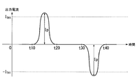
- FIG. 2 shows an example of the waveform of the output current when the output voltage (not shown) is a sine wave.
- the waveform of the output current is not a sine wave, and is 0 in the period from time t10, the period from time t20 to time t30, and the period after time t40. . This is because the reverse voltage is temporarily applied to the diode 311 or the like due to the voltage of the capacitor 316.
- the absolute value of the output current starts to increase when the voltage applied to the diode 311 and the like exceeds the voltage of the capacitor 316 (time t10, t30).
- the energy of the electric power supplied from the inverter 100 to the load 300 is accumulated.
- the energy is released at once, and the output current increases rapidly.
- the peak value I P of the output current becomes a relatively large value.
- An increase in the peak value I P is not preferable because it may cause damage to the switching element 111 and the diode 311 and the like. In particular, such a possibility increases when the load 300 includes an electronic component having a low maximum rated current.
- the power conversion device 10 is configured to appropriately change the waveform of the output voltage based on the measured value of the output current by the ammeter 120. Specifically, a plurality of output voltage waveforms are prepared in advance, and an appropriate waveform is selected from these.
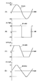
- FIGS. 3A to 3D four waveforms shown in FIGS. 3A to 3D are prepared in advance as output voltage waveforms.
- FIG. 3A shows a normally input sine wave.
- the amplitude of the sine wave that is, the maximum value of the voltage is shown as “voltage V0”.
- first waveform the waveform shown in FIG. 3B
- second waveform the waveform shown in FIG. 3C
- FIG. the waveform shown in FIG. 3C
- third waveform is a trapezoidal wave.
- the first waveform in FIG. 3B is a waveform whose inclination angle (angle with respect to the time axis, which is the horizontal axis) at the time of rising and falling of the voltage is 90 degrees, that is, a rectangular wave.
- the inclination angle at the rise and fall of the voltage is gentler than that of the first waveform.
- the inclination angle at the rise and fall of the voltage is more gradual than the second waveform.
- the periods of the first waveform, the second waveform, and the third waveform are all the same as the period of the first waveform.
- the amplitudes of the first waveform, the second waveform, and the third waveform are the same voltage V1.
- the value of the voltage V1 is smaller than the value of the voltage V0.
- the effective value of the voltage in each of the first waveform, the second waveform, and the third waveform is almost the same as the effective value of the voltage in the first waveform. equal.
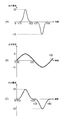
- FIG. 4A shows the waveform of the output current when the output voltage is the sine wave of FIG.
- FIG. 4B shows a waveform of the output current when the output voltage has the first waveform of FIG.
- FIG. 4C shows a waveform of the output current when the output voltage has the second waveform of FIG.
- the output voltage is a sine wave
- the period during which the output current is 0 (the period from time t21 to time t31) is the longest, and the peak of the output current
- the value I P is the largest value (I0).
- the period during which the output current is 0 (the period from time t23 to time t33) is more than that in the case of FIG. It is getting shorter. Further, the peak value I P of the output current in the case of FIG. 4 (A) (I0) less than, larger than the case of FIG. 4 (B) (I1).
- the peak value I P of the output current becomes the largest when the output voltage is a sine wave. Further, when the output voltage is a trapezoidal wave, the peak value I P decreases as the slope at the rise of the voltage increases. For this reason, considering only the suppression of the peak value I P , it is desirable that the waveform of the output voltage is a trapezoidal wave and the gradient at the time of voltage rise is as large as possible.
- ripple pulsesation
- FIG. 4A when the output voltage is a sine wave, almost no ripple occurs.
- FIG. 4B when the output voltage is a rectangular wave, the size of the ripple is maximum.
- the output current peak value I P and the ripple can be changed by appropriately selecting the waveform of the output voltage, but both are in a trade-off relationship.
- the power conversion device 10 switches the waveform of the output voltage depending on the situation.
- first threshold value I TH1 and second threshold value I TH2 are set for the peak value I P.
- the first threshold value I TH1 is a threshold value set as an upper limit value of the peak value I P , and is set as a value smaller than the maximum rated current of the switching element 111 or the like.
- the second threshold value I TH2 is a threshold value set as a lower limit value of the peak value I P and is set as a value smaller than the first threshold value I TH1 .
- the range of the peak value I P defined by the first threshold value I TH1 and the second threshold value I TH2 reliably prevents the switching element 111 and the like from being damaged, and the ripple does not become too large.
- the waveform of the output voltage is switched so that the peak value IP is within an appropriate range as much as possible.
- the output voltage waveform is a sine wave. That is, the output voltage having the waveform shown in FIG. 3A is input to the load 300.
- the peak value I P which is measured by the ammeter 120, whether large is determined than the first threshold I TH1.
- the peak value I P is equal to or less than the first threshold value I TH1 , it is not necessary to suppress the peak value I P by switching the output voltage, and the series of processes shown in FIG. Thereafter, the state where the waveform of the output voltage is a sine wave is continued.
- the process proceeds to S03.
- the waveform of the output voltage is switched from the sine wave to the first waveform. That is, the control unit 130 switches the opening / closing operation of the switching element 111 and the like so that the waveform of the output voltage becomes the first waveform of FIG.
- the peak value I P is the fact that greater than the first threshold I TH1, further accommodated in the first threshold I TH1 or less to suppress the peak value I P It is impossible. Therefore, if it transfers to S05, the control part 130 will shut down the power converter device 10, and will complete
- the process proceeds to S06.
- the peak value I P is whether large is determined than the second threshold I TH2.
- the peak value I P is within the appropriate range. For this reason, since further switching of the output voltage is unnecessary, the series of processes shown in FIG. 6 is terminated. Thereafter, the state where the waveform of the output voltage is the first waveform is continued.
- the process proceeds to S09.
- the peak value I P is whether large is determined than the second threshold I TH2.
- the peak value I P is within the appropriate range. For this reason, since further switching of the output voltage is unnecessary, the series of processes shown in FIG. 6 is terminated. Thereafter, the state where the waveform of the output voltage is the second waveform is continued.
- the process proceeds to S13.
- the transition to S13 means that the peak value IP does not fall within the proper range even when the waveform of the output voltage is switched to any of the waveforms shown in FIG. 3 (however, smaller than the first threshold value ITH1 ). That's what it means. Therefore, in S13, the waveform of the output voltage is returned from the third waveform to a sine wave. That is, the control unit 130 switches the opening / closing operation of the switching element 111 and the like so that the waveform of the output voltage becomes the sine wave of FIG. Thereafter, the series of processes shown in FIG. Thereafter, the state where the waveform of the output voltage is the original sine wave is continued.
- the ammeter 120 is switched waveform of the output voltage on the basis of the output current measured by, an appropriate range as possible peak value I P of the output current Control to be accommodated is executed. Thereby, the suppressing the peak value I P of the output current, compatibility between suppressing noise (ripple) of the output current is achieved.
- output voltage waveforms prepared in advance are not limited to those shown in FIGS. 3 (A) to 3 (D).
- an output voltage waveform as shown in FIGS. 7A to 7D may be prepared in advance, and these waveforms may be appropriately selected.
- the sine wave in FIG. 7 (A) and the first waveform in FIG. 7 (B) are the same as the sine wave in FIG. 3 (A) and the first waveform in FIG. 3 (B), respectively. .
- the second waveform rises to a voltage V01 at an inclination angle of 90 degrees and rises to a voltage V1 at a gentle inclination angle when rising. It has a waveform like this. At the time of falling from the voltage V1, the waveform decreases to a voltage ( ⁇ V01) at an inclination angle of 90 degrees.
- the third waveform rises to the voltage V01 at a tilt angle of 90 degrees at the time of rising, and thereafter to the voltage V1 (than the second waveform). Further, the waveform rises with a gentle inclination angle. At the time of falling from the voltage V1, the waveform decreases to a voltage ( ⁇ V01) at an inclination angle of 90 degrees.
- the waveform of the output voltage waveform prepared in advance is not limited to a trapezoidal wave.
- an output voltage waveform as shown in FIGS. 8A to 8D may be prepared in advance, and these waveforms may be appropriately selected.
- the sine wave in FIG. 8A is the same as the sine wave in FIG.
- the first waveform has a flat top of the same sine wave waveform as in FIG. 8 (A), thereby limiting the output voltage to the voltage V10 or lower. It has a waveform.
- the voltage V10 is set in advance as a voltage smaller than the voltage V0 that is the amplitude of the sine wave.
- the second waveform has a flat top portion of the same sine wave waveform as in FIG. 8A, thereby limiting the output voltage to the voltage V20 or less. It has a waveform.
- the voltage V20 is set in advance as a voltage that is smaller than the voltage V0 that is the amplitude of the sine wave and larger than the voltage V10.
- the third waveform has a flat top of the same sine wave waveform as in FIG. 8 (A), thereby limiting the output voltage to the voltage V30 or lower. It has a waveform.
- the voltage V30 is set in advance as a voltage that is smaller than the voltage V0 that is the amplitude of the sine wave and larger than the voltage V20.
- the effects of the present disclosure can be achieved. It can. Note that processing for selecting an appropriate one of the sine wave, the first waveform, the second waveform, and the third waveform shown in FIGS. 8A to 8D and switching the waveform of the output voltage is performed. Is the same as the processing described with reference to FIG. Therefore, the specific description is omitted.
- control for switching the waveform of the output voltage in accordance with the peak value I P of the measured output current it has been described control for switching the waveform of the output voltage in accordance with the peak value I P of the measured output current.
- embodiments of the present disclosure are not limited to this.
- a mode in which the waveform of the output voltage is switched in accordance with a deviation amount from a predetermined target current waveform may be employed.
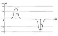
- the target current waveform and the amount of deviation will be described with reference to FIG.
- the target current waveform IDS is a waveform of an output current when the load 300 is a linear load and a sine wave output voltage is input to the load. Therefore, the target current waveform IDS is a sine wave.
- Such a target current waveform IDS can be said to be an ideal output current waveform to be originally supplied to the load 300.
- the target current waveform IDS is desirably set as a waveform having as large an amplitude as possible within a range that does not exceed the maximum rated current of the switching element 111.
- the same waveform as the waveform of the output current shown in FIG. 5 is shown as a line G1.
- the deviation amount ⁇ I is defined as the absolute value of the difference between the actual output current at each time and the value of the target current waveform IDS at the same time.
- the output current waveform does not match the target current waveform IDS. For this reason, the deviation amount ⁇ I changes with time. If the waveform of the output current matches the target current waveform IDS, the deviation amount ⁇ I is always 0.
- the output voltage waveform is a sine wave. That is, the output voltage having the waveform shown in FIG. 3A is input to the load 300.
- the process proceeds to S23.
- the waveform of the output voltage is switched from the sine wave to the first waveform. That is, the control unit 130 switches the opening / closing operation of the switching element 111 and the like so that the waveform of the output voltage becomes the first waveform of FIG.
- the peak value I P is whether large is determined than the first threshold I TH1.
- the process proceeds to S25.
- the peak value I P is the fact that greater than the first threshold I TH1, further accommodated in the first threshold I TH1 or less to suppress the peak value I P It is impossible. Therefore, if transfering to S25, the control part 130 will shut down the power converter device 10, and will complete
- the necessity of shutdown is determined based on the peak value I P that is an absolute current value, not the deviation amount ⁇ I that is a relative current value. This reliably prevents the output current from becoming too large (for example, greater than the maximum rated current of the switching element 111 or the like).
- the process proceeds to S26.
- S26 when the deviation amount ⁇ I is temporarily (or always) not less than the third threshold value I TH3 or temporarily (or always) not more than the fourth threshold value I TH4 , the process proceeds to S27.
- S27 the waveform of the output voltage is switched from the first waveform to the second waveform. That is, the control unit 130 switches the opening / closing operation of the switching element 111 and the like so that the waveform of the output voltage becomes the second waveform of FIG.
- transition to S35 means that the deviation amount ⁇ I has become too large due to switching from the first waveform to the second waveform. For this reason, in S35, the waveform of the output voltage is returned to the first waveform. Thereafter, the series of processes shown in FIG. Thereafter, the state where the waveform of the output voltage is the first waveform is continued.
- transition to S34 means that the deviation amount ⁇ I has become too large due to switching from the second waveform to the third waveform. For this reason, in S34, the waveform of the output voltage is returned to the second waveform. Thereafter, the series of processes shown in FIG. Thereafter, the state where the waveform of the output voltage is the second waveform is continued.
- S32 when the deviation amount ⁇ I is temporarily (or always) equal to or smaller than the fourth threshold value I TH4 , the process proceeds to S33.
- the waveform of the output voltage is returned from the third waveform to a sine wave. That is, the control unit 130 switches the opening / closing operation of the switching element 111 and the like so that the waveform of the output voltage becomes the sine wave of FIG. Thereafter, the series of processes shown in FIG. Thereafter, the state where the waveform of the output voltage is the original sine wave is continued.
- the output voltage waveform is switched based on the output current deviation amount ⁇ I measured by the ammeter 120, and the state where the deviation amount ⁇ I is always small is maintained.
- the peak value I P of the output current becomes too large, and it is to too small is prevented.
Landscapes
- Engineering & Computer Science (AREA)
- Power Engineering (AREA)
- Inverter Devices (AREA)
Priority Applications (1)
| Application Number | Priority Date | Filing Date | Title |
|---|---|---|---|
| US15/547,602 US10270365B2 (en) | 2015-02-16 | 2016-02-05 | Power conversion device |
Applications Claiming Priority (2)
| Application Number | Priority Date | Filing Date | Title |
|---|---|---|---|
| JP2015-027910 | 2015-02-16 | ||
| JP2015027910A JP6669434B2 (ja) | 2015-02-16 | 2015-02-16 | 電力変換装置 |
Publications (1)
| Publication Number | Publication Date |
|---|---|
| WO2016132700A1 true WO2016132700A1 (ja) | 2016-08-25 |
Family
ID=56692102
Family Applications (1)
| Application Number | Title | Priority Date | Filing Date |
|---|---|---|---|
| PCT/JP2016/000604 Ceased WO2016132700A1 (ja) | 2015-02-16 | 2016-02-05 | 電力変換装置 |
Country Status (3)
| Country | Link |
|---|---|
| US (1) | US10270365B2 (enExample) |
| JP (1) | JP6669434B2 (enExample) |
| WO (1) | WO2016132700A1 (enExample) |
Families Citing this family (1)
| Publication number | Priority date | Publication date | Assignee | Title |
|---|---|---|---|---|
| KR102343688B1 (ko) * | 2016-12-09 | 2021-12-27 | 삼성에스디아이 주식회사 | 전력 변환 장치 및 이를 포함하는 무정전 전원 공급 장치 |
Citations (4)
| Publication number | Priority date | Publication date | Assignee | Title |
|---|---|---|---|---|
| JPS58224571A (ja) * | 1982-06-24 | 1983-12-26 | Mitsubishi Electric Corp | パルス幅変調インバ−タ装置の電圧基準波形発生回路 |
| JPH04285473A (ja) * | 1991-03-11 | 1992-10-09 | Toshiba Corp | Dc/ac電源装置 |
| JP2004215321A (ja) * | 2002-12-26 | 2004-07-29 | Ntt Data Corp | 無停電電源装置 |
| JP2008278558A (ja) * | 2007-04-25 | 2008-11-13 | Densei Lambda Kk | 無停電電源装置、交流電力供給装置および負荷機器に応じた交流電圧切替方法 |
Family Cites Families (10)
| Publication number | Priority date | Publication date | Assignee | Title |
|---|---|---|---|---|
| US5191262A (en) * | 1978-12-28 | 1993-03-02 | Nilssen Ole K | Extra cost-effective electronic ballast |
| DE3303223A1 (de) * | 1983-02-01 | 1984-08-09 | Silcon Elektronik As | Stromversorgungsvorrichtung |
| US5260996A (en) * | 1990-12-10 | 1993-11-09 | Reliance Comm/Tec Corporation | Current limited electronic ringing generator |
| US5657220A (en) * | 1995-12-04 | 1997-08-12 | Astec International, Ltd. | Electrical power inverter |
| US7218539B2 (en) * | 2005-03-22 | 2007-05-15 | Delphi Technologies, Inc. | Technique for increasing power capability of a DC-to-AC converter |
| JP2007082317A (ja) | 2005-09-14 | 2007-03-29 | Fuji Electric Fa Components & Systems Co Ltd | 電力システム |
| JP4277127B2 (ja) * | 2007-08-22 | 2009-06-10 | サンケン電気株式会社 | 交流電源装置 |
| JP5281330B2 (ja) * | 2008-07-25 | 2013-09-04 | 本田技研工業株式会社 | インバータ発電機 |
| US9166445B2 (en) * | 2011-09-28 | 2015-10-20 | Eaton Corporation | AC power supply apparatus and methods providing variable voltage waveforms for load transient conditions |
| US9712050B2 (en) * | 2014-07-17 | 2017-07-18 | Infineon Technologies Americas Corp. | Power converter utilizing a resonant half-bridge and charge pump circuit |
-
2015
- 2015-02-16 JP JP2015027910A patent/JP6669434B2/ja active Active
-
2016
- 2016-02-05 WO PCT/JP2016/000604 patent/WO2016132700A1/ja not_active Ceased
- 2016-02-05 US US15/547,602 patent/US10270365B2/en active Active
Patent Citations (4)
| Publication number | Priority date | Publication date | Assignee | Title |
|---|---|---|---|---|
| JPS58224571A (ja) * | 1982-06-24 | 1983-12-26 | Mitsubishi Electric Corp | パルス幅変調インバ−タ装置の電圧基準波形発生回路 |
| JPH04285473A (ja) * | 1991-03-11 | 1992-10-09 | Toshiba Corp | Dc/ac電源装置 |
| JP2004215321A (ja) * | 2002-12-26 | 2004-07-29 | Ntt Data Corp | 無停電電源装置 |
| JP2008278558A (ja) * | 2007-04-25 | 2008-11-13 | Densei Lambda Kk | 無停電電源装置、交流電力供給装置および負荷機器に応じた交流電圧切替方法 |
Also Published As
| Publication number | Publication date |
|---|---|
| US10270365B2 (en) | 2019-04-23 |
| JP6669434B2 (ja) | 2020-03-18 |
| JP2016152657A (ja) | 2016-08-22 |
| US20180062497A1 (en) | 2018-03-01 |
Similar Documents
| Publication | Publication Date | Title |
|---|---|---|
| US8634212B2 (en) | Controller and controlling method for power converter | |
| CN104521097B (zh) | 用于提供不间断电源的装置和方法 | |
| JP6185860B2 (ja) | 双方向コンバータ | |
| KR102698112B1 (ko) | 멀티레벨 변환기를 위한 전압 밸런스 시스템 및 방법 | |
| JP6334336B2 (ja) | 電力変換装置 | |
| US20210257852A1 (en) | Uninterruptible power supply apparatus | |
| US10033182B2 (en) | Bidirectional electrical signal converter | |
| JP2019022313A (ja) | 電力変換装置 | |
| US9515575B2 (en) | Power conversion apparatus and power conversion method | |
| TWI547083B (zh) | 電源轉換器的控制電路及相關方法 | |
| JP6669434B2 (ja) | 電力変換装置 | |
| JP6849546B2 (ja) | 系統連系用電力変換装置 | |
| US10276084B2 (en) | Circuit having a variable output and a converter controller including same | |
| KR101826609B1 (ko) | 3상 3레벨 전력변환장치의 pwm 제어 장치 | |
| KR101478634B1 (ko) | 전력 변환기의 방열 능력 극대화를 위한 선택적 스위칭 방법, 그 방법이 적용되는 에너지 저장 장치, 및 전력 변환 장치 | |
| KR102226290B1 (ko) | Ac-dc 컨버터 | |
| JP5528730B2 (ja) | 電力変換装置 | |
| KR101134854B1 (ko) | 전압 보상 공급 장치 | |
| JP5294908B2 (ja) | 電力変換装置 | |
| JP2014135878A (ja) | 三相コンバータのコントローラ、それを用いた電力変換装置 | |
| TW201521343A (zh) | 電源轉換器及其斜率偵測控制器與方法 | |
| KR20080005273A (ko) | 업스트림 스텝―업 장치를 포함하는 인버터를 동작시키기위한 방법 | |
| JP6907855B2 (ja) | 3レベルチョッパ及びその制御回路 | |
| JP6895067B2 (ja) | 3レベルチョッパ及びその制御回路 | |
| JP7097673B2 (ja) | 系統連系インバータ装置 |
Legal Events
| Date | Code | Title | Description |
|---|---|---|---|
| 121 | Ep: the epo has been informed by wipo that ep was designated in this application |
Ref document number: 16752091 Country of ref document: EP Kind code of ref document: A1 |
|
| WWE | Wipo information: entry into national phase |
Ref document number: 15547602 Country of ref document: US |
|
| NENP | Non-entry into the national phase |
Ref country code: DE |
|
| 122 | Ep: pct application non-entry in european phase |
Ref document number: 16752091 Country of ref document: EP Kind code of ref document: A1 |