WO2016132700A1 - Power conversion device - Google Patents
Power conversion device Download PDFInfo
- Publication number
- WO2016132700A1 WO2016132700A1 PCT/JP2016/000604 JP2016000604W WO2016132700A1 WO 2016132700 A1 WO2016132700 A1 WO 2016132700A1 JP 2016000604 W JP2016000604 W JP 2016000604W WO 2016132700 A1 WO2016132700 A1 WO 2016132700A1
- Authority
- WO
- WIPO (PCT)
- Prior art keywords
- waveform
- output voltage
- power
- current
- output
- Prior art date
Links
Images


Classifications
-
- H—ELECTRICITY
- H02—GENERATION; CONVERSION OR DISTRIBUTION OF ELECTRIC POWER
- H02M—APPARATUS FOR CONVERSION BETWEEN AC AND AC, BETWEEN AC AND DC, OR BETWEEN DC AND DC, AND FOR USE WITH MAINS OR SIMILAR POWER SUPPLY SYSTEMS; CONVERSION OF DC OR AC INPUT POWER INTO SURGE OUTPUT POWER; CONTROL OR REGULATION THEREOF
- H02M7/00—Conversion of ac power input into dc power output; Conversion of dc power input into ac power output
- H02M7/42—Conversion of dc power input into ac power output without possibility of reversal
- H02M7/44—Conversion of dc power input into ac power output without possibility of reversal by static converters
- H02M7/48—Conversion of dc power input into ac power output without possibility of reversal by static converters using discharge tubes with control electrode or semiconductor devices with control electrode
- H02M7/53—Conversion of dc power input into ac power output without possibility of reversal by static converters using discharge tubes with control electrode or semiconductor devices with control electrode using devices of a triode or transistor type requiring continuous application of a control signal
- H02M7/537—Conversion of dc power input into ac power output without possibility of reversal by static converters using discharge tubes with control electrode or semiconductor devices with control electrode using devices of a triode or transistor type requiring continuous application of a control signal using semiconductor devices only, e.g. single switched pulse inverters
- H02M7/5387—Conversion of dc power input into ac power output without possibility of reversal by static converters using discharge tubes with control electrode or semiconductor devices with control electrode using devices of a triode or transistor type requiring continuous application of a control signal using semiconductor devices only, e.g. single switched pulse inverters in a bridge configuration
- H02M7/53871—Conversion of dc power input into ac power output without possibility of reversal by static converters using discharge tubes with control electrode or semiconductor devices with control electrode using devices of a triode or transistor type requiring continuous application of a control signal using semiconductor devices only, e.g. single switched pulse inverters in a bridge configuration with automatic control of output voltage or current
-
- H—ELECTRICITY
- H02—GENERATION; CONVERSION OR DISTRIBUTION OF ELECTRIC POWER
- H02M—APPARATUS FOR CONVERSION BETWEEN AC AND AC, BETWEEN AC AND DC, OR BETWEEN DC AND DC, AND FOR USE WITH MAINS OR SIMILAR POWER SUPPLY SYSTEMS; CONVERSION OF DC OR AC INPUT POWER INTO SURGE OUTPUT POWER; CONTROL OR REGULATION THEREOF
- H02M1/00—Details of apparatus for conversion
- H02M1/32—Means for protecting converters other than automatic disconnection
-
- H—ELECTRICITY
- H02—GENERATION; CONVERSION OR DISTRIBUTION OF ELECTRIC POWER
- H02M—APPARATUS FOR CONVERSION BETWEEN AC AND AC, BETWEEN AC AND DC, OR BETWEEN DC AND DC, AND FOR USE WITH MAINS OR SIMILAR POWER SUPPLY SYSTEMS; CONVERSION OF DC OR AC INPUT POWER INTO SURGE OUTPUT POWER; CONTROL OR REGULATION THEREOF
- H02M7/00—Conversion of ac power input into dc power output; Conversion of dc power input into ac power output
- H02M7/42—Conversion of dc power input into ac power output without possibility of reversal
- H02M7/44—Conversion of dc power input into ac power output without possibility of reversal by static converters
- H02M7/48—Conversion of dc power input into ac power output without possibility of reversal by static converters using discharge tubes with control electrode or semiconductor devices with control electrode
- H02M7/53—Conversion of dc power input into ac power output without possibility of reversal by static converters using discharge tubes with control electrode or semiconductor devices with control electrode using devices of a triode or transistor type requiring continuous application of a control signal
- H02M7/537—Conversion of dc power input into ac power output without possibility of reversal by static converters using discharge tubes with control electrode or semiconductor devices with control electrode using devices of a triode or transistor type requiring continuous application of a control signal using semiconductor devices only, e.g. single switched pulse inverters
- H02M7/539—Conversion of dc power input into ac power output without possibility of reversal by static converters using discharge tubes with control electrode or semiconductor devices with control electrode using devices of a triode or transistor type requiring continuous application of a control signal using semiconductor devices only, e.g. single switched pulse inverters with automatic control of output wave form or frequency
-
- H—ELECTRICITY
- H02—GENERATION; CONVERSION OR DISTRIBUTION OF ELECTRIC POWER
- H02M—APPARATUS FOR CONVERSION BETWEEN AC AND AC, BETWEEN AC AND DC, OR BETWEEN DC AND DC, AND FOR USE WITH MAINS OR SIMILAR POWER SUPPLY SYSTEMS; CONVERSION OF DC OR AC INPUT POWER INTO SURGE OUTPUT POWER; CONTROL OR REGULATION THEREOF
- H02M1/00—Details of apparatus for conversion
- H02M1/0003—Details of control, feedback or regulation circuits
- H02M1/0009—Devices or circuits for detecting current in a converter
-
- H—ELECTRICITY
- H02—GENERATION; CONVERSION OR DISTRIBUTION OF ELECTRIC POWER
- H02M—APPARATUS FOR CONVERSION BETWEEN AC AND AC, BETWEEN AC AND DC, OR BETWEEN DC AND DC, AND FOR USE WITH MAINS OR SIMILAR POWER SUPPLY SYSTEMS; CONVERSION OF DC OR AC INPUT POWER INTO SURGE OUTPUT POWER; CONTROL OR REGULATION THEREOF
- H02M1/00—Details of apparatus for conversion
- H02M1/0048—Circuits or arrangements for reducing losses
- H02M1/0054—Transistor switching losses
-
- H—ELECTRICITY
- H02—GENERATION; CONVERSION OR DISTRIBUTION OF ELECTRIC POWER
- H02M—APPARATUS FOR CONVERSION BETWEEN AC AND AC, BETWEEN AC AND DC, OR BETWEEN DC AND DC, AND FOR USE WITH MAINS OR SIMILAR POWER SUPPLY SYSTEMS; CONVERSION OF DC OR AC INPUT POWER INTO SURGE OUTPUT POWER; CONTROL OR REGULATION THEREOF
- H02M3/00—Conversion of dc power input into dc power output
- H02M3/22—Conversion of dc power input into dc power output with intermediate conversion into ac
- H02M3/24—Conversion of dc power input into dc power output with intermediate conversion into ac by static converters
- H02M3/28—Conversion of dc power input into dc power output with intermediate conversion into ac by static converters using discharge tubes with control electrode or semiconductor devices with control electrode to produce the intermediate ac
- H02M3/325—Conversion of dc power input into dc power output with intermediate conversion into ac by static converters using discharge tubes with control electrode or semiconductor devices with control electrode to produce the intermediate ac using devices of a triode or a transistor type requiring continuous application of a control signal
- H02M3/335—Conversion of dc power input into dc power output with intermediate conversion into ac by static converters using discharge tubes with control electrode or semiconductor devices with control electrode to produce the intermediate ac using devices of a triode or a transistor type requiring continuous application of a control signal using semiconductor devices only
- H02M3/337—Conversion of dc power input into dc power output with intermediate conversion into ac by static converters using discharge tubes with control electrode or semiconductor devices with control electrode to produce the intermediate ac using devices of a triode or a transistor type requiring continuous application of a control signal using semiconductor devices only in push-pull configuration
- H02M3/3376—Conversion of dc power input into dc power output with intermediate conversion into ac by static converters using discharge tubes with control electrode or semiconductor devices with control electrode to produce the intermediate ac using devices of a triode or a transistor type requiring continuous application of a control signal using semiconductor devices only in push-pull configuration with automatic control of output voltage or current
-
- Y—GENERAL TAGGING OF NEW TECHNOLOGICAL DEVELOPMENTS; GENERAL TAGGING OF CROSS-SECTIONAL TECHNOLOGIES SPANNING OVER SEVERAL SECTIONS OF THE IPC; TECHNICAL SUBJECTS COVERED BY FORMER USPC CROSS-REFERENCE ART COLLECTIONS [XRACs] AND DIGESTS
- Y02—TECHNOLOGIES OR APPLICATIONS FOR MITIGATION OR ADAPTATION AGAINST CLIMATE CHANGE
- Y02B—CLIMATE CHANGE MITIGATION TECHNOLOGIES RELATED TO BUILDINGS, e.g. HOUSING, HOUSE APPLIANCES OR RELATED END-USER APPLICATIONS
- Y02B70/00—Technologies for an efficient end-user side electric power management and consumption
- Y02B70/10—Technologies improving the efficiency by using switched-mode power supplies [SMPS], i.e. efficient power electronics conversion e.g. power factor correction or reduction of losses in power supplies or efficient standby modes
Definitions
- This disclosure relates to a power converter that converts DC power supplied from a power supply source into AC power and supplies the AC power to a load.
- Power obtained from power supply sources such as solar cells, fuel cells, and storage batteries is rarely supplied directly to the load as it is, boosted as necessary, and converted from direct current to alternating current. Later supplied to the load.
- the power conversion device described in Patent Literature 1 below includes a converter for boosting DC power supplied from a power supply source (power generation means) and an inverter for converting DC power to AC power.
- the inverter includes a plurality of switching elements, and performs conversion from DC power to AC power by switching opening and closing of the switching elements with a predetermined duty.
- the switching element is operated so that the waveform of the voltage output as AC power is not a sine wave but a trapezoidal wave. Thereby, switching loss is reduced and the conversion efficiency in a power converter device is improved.
- the relationship between the voltage and current supplied to the load may not be linear.
- the waveform of the output voltage from the power converter is a sine wave
- the output current from the power converter is not a sine wave.
- a capacitor input type rectifier circuit input AC power is converted to DC power by a diode bridge composed of a plurality of diodes.
- the voltage waveform of the power input to the diode bridge is a sine wave
- the peak of the waveform of the output current from the power converter is caused by the current flowing only when the forward voltage is applied to the diode.
- the waveform of the output voltage from the power converter is a trapezoidal wave instead of a sine wave.
- the AC power whose output voltage waveform is a trapezoidal wave includes a high-frequency component, so-called ripples are likely to occur in the output current from the power converter.
- noise due to ripple may affect the operation of the load.
- the waveform of the output voltage from the power converter is a sine wave.
- Patent Document 1 proposes that the output current be a trapezoidal wave, and no consideration is given to reconciling the above two problems.
- the present disclosure aims to provide a power conversion device that can further suppress noise of the output current while suppressing the peak of the waveform of the output current.
- a power converter includes an inverter that converts DC power supplied from a power supply source into AC power by an operation of a switching element, and outputs the AC power toward a load; A current measurement unit that measures the output current of the inverter, and a control unit that changes the output voltage waveform of the inverter by controlling the operation of the switching element, and the control unit outputs based on the measured output current Change the voltage waveform.
- the control unit controls the operation of the switching element so as to change the output voltage waveform based on the measured output current. For example, control that appropriately changes the output voltage waveform so that noise is suppressed as much as possible within a range in which the peak of the measured output current can be suppressed to a predetermined value or less (for example, an output voltage waveform that is a trapezoidal wave is more By controlling so as to approach a sine wave, it is possible to achieve both suppression of the peak of the waveform of the output current and suppression of noise of the output current. Therefore, a power conversion device that can further suppress noise of the output current while suppressing the peak of the waveform of the output current is provided.
- the configuration of the power conversion apparatus 10 according to the present embodiment will be described with reference to FIG.
- the power conversion device 10 converts DC power supplied from the power supply device 200 (power supply source) into AC power and outputs it to the load 300.
- the power supply device 200 is a power generation device that generates DC power and supplies it to the outside, and is specifically a solar cell device.
- the specific mode of the power supply device is not particularly limited.
- the power supply device 200 may be a wind power generator or a fuel cell device. Moreover, it may replace with what generates direct-current power by electric power generation, and may be an apparatus which supplies the electric power stored beforehand, for example like a storage battery, outside.
- the load 300 is a device that operates upon receiving AC power.
- the load 300 includes power input terminals 331 and 332, diodes 311, 312, 313, and 314, a capacitor 316, and a resistor 317.
- the power input terminals 331 and 332 are a pair of terminals to which AC power from the power converter 10 is input.
- the four diodes 311, 312, 313, 314 and the capacitor 316 form a capacitor input type rectifier circuit.
- a smoothing reactor 315 is disposed between the power input terminal 331 and the capacitor input type rectifier circuit.
- the AC power When AC power is input to the power input terminals 331 and 332, the AC power is converted into DC power by the capacitor input rectifier circuit, and supplied to the resistor 317 for consumption.
- the resistor 317 virtually represents the entire portion operated by the power converted into DC power by the rectifier circuit as a single electrical resistance.
- the power conversion device 10 disposed between the power supply device 200 and the load 300 includes an inverter 100, a voltmeter 110, an ammeter 120, and a control unit 130.
- the inverter 100 is a part that converts DC power into AC power.
- the inverter 100 includes power input terminals 131 and 132, switching elements 111, 112, 113, and 114, and power output terminals 141 and 142.
- the power input terminals 131 and 132 are a pair of terminals to which DC power from the power supply device 200 is input.
- a smoothing capacitor 115 is connected between the power input terminal 131 and the power input terminal 132.
- the switching elements 111, 112, 113, and 114 are all the same IGBT, and constitute a full bridge inverter circuit as a whole.
- the switching elements 111, 112, 113, and 114 are opened and closed based on a control signal transmitted from the control unit 130, which will be described later, thereby converting DC power to AC power.
- the power output terminals 141 and 142 are a pair of terminals for outputting the AC power generated by the full bridge inverter circuit to the outside (that is, to the load 300). Smoothing reactors 116 and 117 and a capacitor 118 are arranged between the full bridge inverter circuit and the power output terminals 141 and 142.
- the voltmeter 110 measures a voltage between the power output terminal 141 and the power output terminal 142, that is, a voltage of AC power output from the power conversion device 10 (hereinafter also referred to as “output voltage”). .
- the value of the output voltage measured by the voltmeter 110 is always input to the control unit 130.
- the ammeter 120 measures the current output from the power output terminal 141, that is, the current of AC power output from the power conversion device 10 (hereinafter also referred to as “output current”). The value of the output current measured by the ammeter 120 is always input to the control unit 130.
- the control unit 130 is a computer system including a CPU, a ROM, a RAM, an input / output interface, and the like, and controls the overall operation of the power conversion apparatus 10. As already described, the control unit 130 transmits a control signal for controlling the opening / closing operations of the switching elements 111, 112, 113, and 114 to the inverter 100. Thereby, the power conversion operation in the inverter 100 is controlled, and the waveform of the output voltage is adjusted.
- the capacitor input type rectifier circuit provided in the load 300 is known as a so-called “non-linear” circuit. That is, in the capacitor input type rectifier circuit, the relationship between the voltage input to the circuit and the current flowing therewith is not linear.
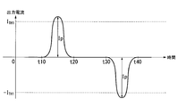
- FIG. 2 shows an example of the waveform of the output current when the output voltage (not shown) is a sine wave.
- the waveform of the output current is not a sine wave, and is 0 in the period from time t10, the period from time t20 to time t30, and the period after time t40. . This is because the reverse voltage is temporarily applied to the diode 311 or the like due to the voltage of the capacitor 316.
- the absolute value of the output current starts to increase when the voltage applied to the diode 311 and the like exceeds the voltage of the capacitor 316 (time t10, t30).
- the energy of the electric power supplied from the inverter 100 to the load 300 is accumulated.
- the energy is released at once, and the output current increases rapidly.
- the peak value I P of the output current becomes a relatively large value.
- An increase in the peak value I P is not preferable because it may cause damage to the switching element 111 and the diode 311 and the like. In particular, such a possibility increases when the load 300 includes an electronic component having a low maximum rated current.
- the power conversion device 10 is configured to appropriately change the waveform of the output voltage based on the measured value of the output current by the ammeter 120. Specifically, a plurality of output voltage waveforms are prepared in advance, and an appropriate waveform is selected from these.
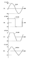
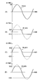
- FIGS. 3A to 3D four waveforms shown in FIGS. 3A to 3D are prepared in advance as output voltage waveforms.
- FIG. 3A shows a normally input sine wave.
- the amplitude of the sine wave that is, the maximum value of the voltage is shown as “voltage V0”.
- first waveform the waveform shown in FIG. 3B
- second waveform the waveform shown in FIG. 3C
- FIG. the waveform shown in FIG. 3C
- third waveform is a trapezoidal wave.
- the first waveform in FIG. 3B is a waveform whose inclination angle (angle with respect to the time axis, which is the horizontal axis) at the time of rising and falling of the voltage is 90 degrees, that is, a rectangular wave.
- the inclination angle at the rise and fall of the voltage is gentler than that of the first waveform.
- the inclination angle at the rise and fall of the voltage is more gradual than the second waveform.
- the periods of the first waveform, the second waveform, and the third waveform are all the same as the period of the first waveform.
- the amplitudes of the first waveform, the second waveform, and the third waveform are the same voltage V1.
- the value of the voltage V1 is smaller than the value of the voltage V0.
- the effective value of the voltage in each of the first waveform, the second waveform, and the third waveform is almost the same as the effective value of the voltage in the first waveform. equal.
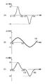
- FIG. 4A shows the waveform of the output current when the output voltage is the sine wave of FIG.
- FIG. 4B shows a waveform of the output current when the output voltage has the first waveform of FIG.
- FIG. 4C shows a waveform of the output current when the output voltage has the second waveform of FIG.
- the output voltage is a sine wave
- the period during which the output current is 0 (the period from time t21 to time t31) is the longest, and the peak of the output current
- the value I P is the largest value (I0).
- the period during which the output current is 0 (the period from time t23 to time t33) is more than that in the case of FIG. It is getting shorter. Further, the peak value I P of the output current in the case of FIG. 4 (A) (I0) less than, larger than the case of FIG. 4 (B) (I1).
- the peak value I P of the output current becomes the largest when the output voltage is a sine wave. Further, when the output voltage is a trapezoidal wave, the peak value I P decreases as the slope at the rise of the voltage increases. For this reason, considering only the suppression of the peak value I P , it is desirable that the waveform of the output voltage is a trapezoidal wave and the gradient at the time of voltage rise is as large as possible.
- ripple pulsesation
- FIG. 4A when the output voltage is a sine wave, almost no ripple occurs.
- FIG. 4B when the output voltage is a rectangular wave, the size of the ripple is maximum.
- the output current peak value I P and the ripple can be changed by appropriately selecting the waveform of the output voltage, but both are in a trade-off relationship.
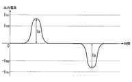
- the power conversion device 10 switches the waveform of the output voltage depending on the situation.
- first threshold value I TH1 and second threshold value I TH2 are set for the peak value I P.
- the first threshold value I TH1 is a threshold value set as an upper limit value of the peak value I P , and is set as a value smaller than the maximum rated current of the switching element 111 or the like.
- the second threshold value I TH2 is a threshold value set as a lower limit value of the peak value I P and is set as a value smaller than the first threshold value I TH1 .
- the range of the peak value I P defined by the first threshold value I TH1 and the second threshold value I TH2 reliably prevents the switching element 111 and the like from being damaged, and the ripple does not become too large.
- the waveform of the output voltage is switched so that the peak value IP is within an appropriate range as much as possible.
- the output voltage waveform is a sine wave. That is, the output voltage having the waveform shown in FIG. 3A is input to the load 300.
- the peak value I P which is measured by the ammeter 120, whether large is determined than the first threshold I TH1.
- the peak value I P is equal to or less than the first threshold value I TH1 , it is not necessary to suppress the peak value I P by switching the output voltage, and the series of processes shown in FIG. Thereafter, the state where the waveform of the output voltage is a sine wave is continued.
- the process proceeds to S03.
- the waveform of the output voltage is switched from the sine wave to the first waveform. That is, the control unit 130 switches the opening / closing operation of the switching element 111 and the like so that the waveform of the output voltage becomes the first waveform of FIG.
- the peak value I P is the fact that greater than the first threshold I TH1, further accommodated in the first threshold I TH1 or less to suppress the peak value I P It is impossible. Therefore, if it transfers to S05, the control part 130 will shut down the power converter device 10, and will complete
- the process proceeds to S06.
- the peak value I P is whether large is determined than the second threshold I TH2.
- the peak value I P is within the appropriate range. For this reason, since further switching of the output voltage is unnecessary, the series of processes shown in FIG. 6 is terminated. Thereafter, the state where the waveform of the output voltage is the first waveform is continued.
- the process proceeds to S09.
- the peak value I P is whether large is determined than the second threshold I TH2.
- the peak value I P is within the appropriate range. For this reason, since further switching of the output voltage is unnecessary, the series of processes shown in FIG. 6 is terminated. Thereafter, the state where the waveform of the output voltage is the second waveform is continued.
- the process proceeds to S13.
- the transition to S13 means that the peak value IP does not fall within the proper range even when the waveform of the output voltage is switched to any of the waveforms shown in FIG. 3 (however, smaller than the first threshold value ITH1 ). That's what it means. Therefore, in S13, the waveform of the output voltage is returned from the third waveform to a sine wave. That is, the control unit 130 switches the opening / closing operation of the switching element 111 and the like so that the waveform of the output voltage becomes the sine wave of FIG. Thereafter, the series of processes shown in FIG. Thereafter, the state where the waveform of the output voltage is the original sine wave is continued.
- the ammeter 120 is switched waveform of the output voltage on the basis of the output current measured by, an appropriate range as possible peak value I P of the output current Control to be accommodated is executed. Thereby, the suppressing the peak value I P of the output current, compatibility between suppressing noise (ripple) of the output current is achieved.
- output voltage waveforms prepared in advance are not limited to those shown in FIGS. 3 (A) to 3 (D).
- an output voltage waveform as shown in FIGS. 7A to 7D may be prepared in advance, and these waveforms may be appropriately selected.
- the sine wave in FIG. 7 (A) and the first waveform in FIG. 7 (B) are the same as the sine wave in FIG. 3 (A) and the first waveform in FIG. 3 (B), respectively. .
- the second waveform rises to a voltage V01 at an inclination angle of 90 degrees and rises to a voltage V1 at a gentle inclination angle when rising. It has a waveform like this. At the time of falling from the voltage V1, the waveform decreases to a voltage ( ⁇ V01) at an inclination angle of 90 degrees.
- the third waveform rises to the voltage V01 at a tilt angle of 90 degrees at the time of rising, and thereafter to the voltage V1 (than the second waveform). Further, the waveform rises with a gentle inclination angle. At the time of falling from the voltage V1, the waveform decreases to a voltage ( ⁇ V01) at an inclination angle of 90 degrees.
- the waveform of the output voltage waveform prepared in advance is not limited to a trapezoidal wave.
- an output voltage waveform as shown in FIGS. 8A to 8D may be prepared in advance, and these waveforms may be appropriately selected.
- the sine wave in FIG. 8A is the same as the sine wave in FIG.
- the first waveform has a flat top of the same sine wave waveform as in FIG. 8 (A), thereby limiting the output voltage to the voltage V10 or lower. It has a waveform.
- the voltage V10 is set in advance as a voltage smaller than the voltage V0 that is the amplitude of the sine wave.
- the second waveform has a flat top portion of the same sine wave waveform as in FIG. 8A, thereby limiting the output voltage to the voltage V20 or less. It has a waveform.
- the voltage V20 is set in advance as a voltage that is smaller than the voltage V0 that is the amplitude of the sine wave and larger than the voltage V10.
- the third waveform has a flat top of the same sine wave waveform as in FIG. 8 (A), thereby limiting the output voltage to the voltage V30 or lower. It has a waveform.
- the voltage V30 is set in advance as a voltage that is smaller than the voltage V0 that is the amplitude of the sine wave and larger than the voltage V20.
- the effects of the present disclosure can be achieved. It can. Note that processing for selecting an appropriate one of the sine wave, the first waveform, the second waveform, and the third waveform shown in FIGS. 8A to 8D and switching the waveform of the output voltage is performed. Is the same as the processing described with reference to FIG. Therefore, the specific description is omitted.
- control for switching the waveform of the output voltage in accordance with the peak value I P of the measured output current it has been described control for switching the waveform of the output voltage in accordance with the peak value I P of the measured output current.
- embodiments of the present disclosure are not limited to this.
- a mode in which the waveform of the output voltage is switched in accordance with a deviation amount from a predetermined target current waveform may be employed.
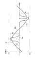
- the target current waveform and the amount of deviation will be described with reference to FIG.
- the target current waveform IDS is a waveform of an output current when the load 300 is a linear load and a sine wave output voltage is input to the load. Therefore, the target current waveform IDS is a sine wave.
- Such a target current waveform IDS can be said to be an ideal output current waveform to be originally supplied to the load 300.
- the target current waveform IDS is desirably set as a waveform having as large an amplitude as possible within a range that does not exceed the maximum rated current of the switching element 111.
- the same waveform as the waveform of the output current shown in FIG. 5 is shown as a line G1.
- the deviation amount ⁇ I is defined as the absolute value of the difference between the actual output current at each time and the value of the target current waveform IDS at the same time.
- the output current waveform does not match the target current waveform IDS. For this reason, the deviation amount ⁇ I changes with time. If the waveform of the output current matches the target current waveform IDS, the deviation amount ⁇ I is always 0.
- the output voltage waveform is a sine wave. That is, the output voltage having the waveform shown in FIG. 3A is input to the load 300.
- the process proceeds to S23.
- the waveform of the output voltage is switched from the sine wave to the first waveform. That is, the control unit 130 switches the opening / closing operation of the switching element 111 and the like so that the waveform of the output voltage becomes the first waveform of FIG.
- the peak value I P is whether large is determined than the first threshold I TH1.
- the process proceeds to S25.
- the peak value I P is the fact that greater than the first threshold I TH1, further accommodated in the first threshold I TH1 or less to suppress the peak value I P It is impossible. Therefore, if transfering to S25, the control part 130 will shut down the power converter device 10, and will complete
- the necessity of shutdown is determined based on the peak value I P that is an absolute current value, not the deviation amount ⁇ I that is a relative current value. This reliably prevents the output current from becoming too large (for example, greater than the maximum rated current of the switching element 111 or the like).
- the process proceeds to S26.
- S26 when the deviation amount ⁇ I is temporarily (or always) not less than the third threshold value I TH3 or temporarily (or always) not more than the fourth threshold value I TH4 , the process proceeds to S27.
- S27 the waveform of the output voltage is switched from the first waveform to the second waveform. That is, the control unit 130 switches the opening / closing operation of the switching element 111 and the like so that the waveform of the output voltage becomes the second waveform of FIG.
- transition to S35 means that the deviation amount ⁇ I has become too large due to switching from the first waveform to the second waveform. For this reason, in S35, the waveform of the output voltage is returned to the first waveform. Thereafter, the series of processes shown in FIG. Thereafter, the state where the waveform of the output voltage is the first waveform is continued.
- transition to S34 means that the deviation amount ⁇ I has become too large due to switching from the second waveform to the third waveform. For this reason, in S34, the waveform of the output voltage is returned to the second waveform. Thereafter, the series of processes shown in FIG. Thereafter, the state where the waveform of the output voltage is the second waveform is continued.
- S32 when the deviation amount ⁇ I is temporarily (or always) equal to or smaller than the fourth threshold value I TH4 , the process proceeds to S33.
- the waveform of the output voltage is returned from the third waveform to a sine wave. That is, the control unit 130 switches the opening / closing operation of the switching element 111 and the like so that the waveform of the output voltage becomes the sine wave of FIG. Thereafter, the series of processes shown in FIG. Thereafter, the state where the waveform of the output voltage is the original sine wave is continued.
- the output voltage waveform is switched based on the output current deviation amount ⁇ I measured by the ammeter 120, and the state where the deviation amount ⁇ I is always small is maintained.
- the peak value I P of the output current becomes too large, and it is to too small is prevented.
Abstract
A power conversion device (10) provided with: an inverter (100) for converting direct current power supplied by a power source device (200) to alternating current power due to the operation of switching elements (111, 112, 113, 114), and outputting the alternating current power towards a load (300); an ammeter (120) for measuring the output current of the inverter (100); and a control unit (130) for changing the output voltage waveform of the inverter (100) by controlling the operation of the switching elements (111, 112, 113, 114). The control unit (130) changes the output voltage waveform on the basis of the measured output current.
Description
本出願は、2015年2月16日に出願された日本出願番号2015-27910号に基づくもので、ここにその記載内容を援用する。
This application is based on Japanese Patent Application No. 2015-27910 filed on February 16, 2015, the contents of which are incorporated herein by reference.
本開示は、電力供給源から供給される直流電力を、交流電力に変換して負荷に供給する電力変換装置に関する。
This disclosure relates to a power converter that converts DC power supplied from a power supply source into AC power and supplies the AC power to a load.
太陽電池、燃料電池、蓄電池等の電力供給源から得られる電力は、そのまま負荷に対して直接供給されることは稀であり、必要に応じて昇圧され、直流から交流への電力変換がなされた後に負荷に供給される。
Power obtained from power supply sources such as solar cells, fuel cells, and storage batteries is rarely supplied directly to the load as it is, boosted as necessary, and converted from direct current to alternating current. Later supplied to the load.
このような電力変換を行うための電力変換装置としては、これまでに種々の態様のものが提案されている。下記特許文献1に記載の電力変換装置は、電力供給源(発電手段)から供給された直流電力を昇圧するためのコンバータと、直流電力を交流電力に変換するためのインバータとを備えている。
Various types of power conversion devices for performing such power conversion have been proposed so far. The power conversion device described in Patent Literature 1 below includes a converter for boosting DC power supplied from a power supply source (power generation means) and an inverter for converting DC power to AC power.
インバータは、複数のスイッチング素子を備えており、当該スイッチング素子の開閉を所定のデューティで切り替えることにより、直流電力から交流電力への変換を行うものである。下記特許文献1に記載の電力変換装置では、交流電力として出力される電圧の波形が、正弦波ではなく台形波となるようにスイッチング素子を動作させている。これにより、スイッチング損失を低減し、電力変換装置における変換効率を向上させている。
The inverter includes a plurality of switching elements, and performs conversion from DC power to AC power by switching opening and closing of the switching elements with a predetermined duty. In the power conversion device described in Patent Document 1 below, the switching element is operated so that the waveform of the voltage output as AC power is not a sine wave but a trapezoidal wave. Thereby, switching loss is reduced and the conversion efficiency in a power converter device is improved.
ところで、電力変換装置から交流電力が供給される負荷の種類によっては、当該負荷に供給される電圧と電流との関係が線形とはならない場合がある。例えば、負荷の電力入力部にコンデンサインプット型の整流回路が設けられているような場合には、電力変換装置からの出力電圧の波形が正弦波であったとしても、電力変換装置からの出力電流(つまり、負荷への入力電流)の波形は正弦波とならない。
By the way, depending on the type of load supplied with AC power from the power converter, the relationship between the voltage and current supplied to the load may not be linear. For example, when a capacitor input type rectifier circuit is provided in the power input section of the load, even if the waveform of the output voltage from the power converter is a sine wave, the output current from the power converter The waveform of (that is, the input current to the load) is not a sine wave.
コンデンサインプット型の整流回路では、複数のダイオードからなるダイオードブリッジにより、入力された交流電力が直流電力に変換される。ダイオードブリッジに入力される電力の電圧波形が正弦波である場合には、ダイオードに順方向電圧がかかった場合にのみ電流が流れることに起因して、電力変換装置からの出力電流の波形のピークが大きくなってしまう傾向がある。このため、スイッチング素子を流れる電流が最大定格電流を超えてしまうことが懸念される。
In a capacitor input type rectifier circuit, input AC power is converted to DC power by a diode bridge composed of a plurality of diodes. When the voltage waveform of the power input to the diode bridge is a sine wave, the peak of the waveform of the output current from the power converter is caused by the current flowing only when the forward voltage is applied to the diode. Tend to be larger. For this reason, there is a concern that the current flowing through the switching element exceeds the maximum rated current.
当該ピークを抑制することにのみ鑑みれば、電力変換装置からの出力電圧の波形を正弦波ではなく台形波とすることが望ましい。しかしながら、出力電圧の波形が台形波であるような交流電力には高周波の成分が含まれるので、電力変換装置からの出力電流において所謂リプルが発生しやすくなる。その結果、リプルによるノイズが負荷の動作に影響を及ぼしてしまう可能性がある。かかるノイズを低減することにのみ鑑みれば、電力変換装置からの出力電圧の波形は正弦波である方が望ましい。
Considering only the suppression of the peak, it is desirable that the waveform of the output voltage from the power converter is a trapezoidal wave instead of a sine wave. However, since the AC power whose output voltage waveform is a trapezoidal wave includes a high-frequency component, so-called ripples are likely to occur in the output current from the power converter. As a result, noise due to ripple may affect the operation of the load. In view of only reducing such noise, it is desirable that the waveform of the output voltage from the power converter is a sine wave.
このように、非線形の負荷が接続される電力変換装置においては、出力電流の波形のピークを抑制することと、出力電流のノイズを抑制することとを両立させる必要がある。上記特許文献1は、出力電流を台形波にすることのみを提案するものであって、上記二つの課題を両立させることについては何ら考慮がなされていない。
Thus, in a power converter to which a non-linear load is connected, it is necessary to satisfy both suppression of the peak of the waveform of the output current and suppression of noise of the output current. The above-mentioned Patent Document 1 proposes that the output current be a trapezoidal wave, and no consideration is given to reconciling the above two problems.
本開示は、出力電流の波形のピークを抑制しながら、更に出力電流のノイズをも抑制することのできる電力変換装置を提供することを目的とする。
The present disclosure aims to provide a power conversion device that can further suppress noise of the output current while suppressing the peak of the waveform of the output current.
本開示の一態様によれば、電力変換装置は、電力供給源から供給される直流電力を、スイッチング素子の動作によって交流電力に変換し、当該交流電力を負荷に向けて出力するインバータと、インバータの出力電流を計測する電流計測部と、スイッチング素子の動作を制御することにより、インバータの出力電圧波形を変化させる制御部と、を備え、制御部は、計測された出力電流に基づいて、出力電圧波形を変化させる。
According to one aspect of the present disclosure, a power converter includes an inverter that converts DC power supplied from a power supply source into AC power by an operation of a switching element, and outputs the AC power toward a load; A current measurement unit that measures the output current of the inverter, and a control unit that changes the output voltage waveform of the inverter by controlling the operation of the switching element, and the control unit outputs based on the measured output current Change the voltage waveform.
このような構成の電力変換装置では、計測された出力電流に基づいて出力電圧波形を変化させるよう、制御部によるスイッチング素子の動作の制御が実行される。例えば、計測された出力電流のピークを所定値以下に抑制し得る範囲で、可能な限りノイズが抑制されるような出力電圧波形に適宜変更する制御(例えば、台形波である出力電圧波形をより正弦波に近づけるような制御)によって、出力電流の波形のピークの抑制と、出力電流のノイズの抑制とを両立させることができる。
よって、出力電流の波形のピークを抑制しながら、更に出力電流のノイズをも抑制することのできる電力変換装置が提供される。 In the power conversion device having such a configuration, the control unit controls the operation of the switching element so as to change the output voltage waveform based on the measured output current. For example, control that appropriately changes the output voltage waveform so that noise is suppressed as much as possible within a range in which the peak of the measured output current can be suppressed to a predetermined value or less (for example, an output voltage waveform that is a trapezoidal wave is more By controlling so as to approach a sine wave, it is possible to achieve both suppression of the peak of the waveform of the output current and suppression of noise of the output current.
Therefore, a power conversion device that can further suppress noise of the output current while suppressing the peak of the waveform of the output current is provided.
本開示についての上記目的およびその他の目的、特徴や利点は、添付の図面を参照しながら下記の詳細な記述により、より明確になる。図面において、
本開示の実施形態に係る電力変換装置の構成を模式的に示す図である。
電力変換装置の出力電流波形を示すグラフである。
(A)~(D)は電力変換装置の出力電圧波形を示すグラフである。
(A)~(C)は電力変換装置の出力電流波形を示すグラフである。
電力変換装置の出力電流波形を示すグラフである。
電力変換装置で行われる処理の流れを示すフローチャートである。
(A)~(D)は電力変換装置の出力電圧波形を示すグラフである。
(A)~(D)は電力変換装置の出力電圧波形を示すグラフである。
出力電流の乖離量を説明するための図である。
電力変換装置で行われる処理の流れを示すフローチャートである。
The above and other objects, features and advantages of the present disclosure will become more apparent from the following detailed description with reference to the accompanying drawings. In the drawing
It is a figure showing typically the composition of the power converter concerning the embodiment of this indication. It is a graph which shows the output current waveform of a power converter device. (A) to (D) are graphs showing output voltage waveforms of the power converter. (A) to (C) are graphs showing output current waveforms of the power converter. It is a graph which shows the output current waveform of a power converter device. It is a flowchart which shows the flow of the process performed with a power converter device. (A) to (D) are graphs showing output voltage waveforms of the power converter. (A) to (D) are graphs showing output voltage waveforms of the power converter. It is a figure for demonstrating the deviation | shift amount of an output current. It is a flowchart which shows the flow of the process performed with a power converter device.
以下、添付図面を参照しながら本開示の実施形態について説明する。説明の理解を容易にするため、各図面において同一の構成要素に対しては可能な限り同一の符号を付して、重複する説明は省略する。
Hereinafter, embodiments of the present disclosure will be described with reference to the accompanying drawings. In order to facilitate the understanding of the description, the same constituent elements in the drawings will be denoted by the same reference numerals as much as possible, and redundant description will be omitted.
図1を参照しながら、本実施形態に係る電力変換装置10の構成について説明する。電力変換装置10は、電源装置200(電力供給源)から供給される直流電力を、交流電力に変換して負荷300に向けて出力するものである。
The configuration of the power conversion apparatus 10 according to the present embodiment will be described with reference to FIG. The power conversion device 10 converts DC power supplied from the power supply device 200 (power supply source) into AC power and outputs it to the load 300.
電源装置200は、直流電力を発生させ外部に供給する発電装置であり、具体的には太陽電池装置である。ただし、本開示を実施するにあたっては、電源装置の具体的な態様は特に限定されない。電源装置200は、風力発電装置や燃料電池装置であってもよい。また、発電によって直流電力を発生させるものに換えて、例えば蓄電池のように、予め蓄えられた電力を外部に供給するような装置であってもよい。
The power supply device 200 is a power generation device that generates DC power and supplies it to the outside, and is specifically a solar cell device. However, in implementing the present disclosure, the specific mode of the power supply device is not particularly limited. The power supply device 200 may be a wind power generator or a fuel cell device. Moreover, it may replace with what generates direct-current power by electric power generation, and may be an apparatus which supplies the electric power stored beforehand, for example like a storage battery, outside.
負荷300は、交流電力の供給を受けて動作する機器である。負荷300は、電力入力端子331、332と、ダイオード311、312、313、314と、コンデンサ316と、抵抗317とを備えている。
The load 300 is a device that operates upon receiving AC power. The load 300 includes power input terminals 331 and 332, diodes 311, 312, 313, and 314, a capacitor 316, and a resistor 317.
電力入力端子331、332は、電力変換装置10からの交流電力が入力される一対の端子である。4つのダイオード311、312、313、314及びコンデンサ316は、コンデンサインプット型整流回路を形成している。電力入力端子331とコンデンサインプット型整流回路との間には、平滑リアクトル315が配置されている。
The power input terminals 331 and 332 are a pair of terminals to which AC power from the power converter 10 is input. The four diodes 311, 312, 313, 314 and the capacitor 316 form a capacitor input type rectifier circuit. A smoothing reactor 315 is disposed between the power input terminal 331 and the capacitor input type rectifier circuit.
電力入力端子331、332に交流電力が入力されると、当該交流電力はコンデンサインプット型整流回路によって直流電力に変換され、抵抗317に供給され消費される。尚、抵抗317は、当該整流回路によって直流電力に変換された電力により動作する部分の全体を、仮想的に単一の電気抵抗として示したものである。
When AC power is input to the power input terminals 331 and 332, the AC power is converted into DC power by the capacitor input rectifier circuit, and supplied to the resistor 317 for consumption. Note that the resistor 317 virtually represents the entire portion operated by the power converted into DC power by the rectifier circuit as a single electrical resistance.
電源装置200と負荷300との間に配置された電力変換装置10は、インバータ100と、電圧計110と、電流計120と、制御部130とを備えている。
The power conversion device 10 disposed between the power supply device 200 and the load 300 includes an inverter 100, a voltmeter 110, an ammeter 120, and a control unit 130.
インバータ100は、直流電力を交流電力に変換する部分である。インバータ100は、電力入力端子131、132と、スイッチング素子111、112、113、114と、電力出力端子141、142とを備えている。
The inverter 100 is a part that converts DC power into AC power. The inverter 100 includes power input terminals 131 and 132, switching elements 111, 112, 113, and 114, and power output terminals 141 and 142.
電力入力端子131、132は、電源装置200からの直流電力が入力される一対の端子である。電力入力端子131と電力入力端子132との間には、平滑用のコンデンサ115が接続されている。
The power input terminals 131 and 132 are a pair of terminals to which DC power from the power supply device 200 is input. A smoothing capacitor 115 is connected between the power input terminal 131 and the power input terminal 132.
スイッチング素子111、112、113、114は、いずれも同一のIGBTであり、全体でフルブリッジインバータ回路を構成している。後述の制御部130から送信される制御信号に基づいて、スイッチング素子111、112、113、114の開閉動作が行われ、これにより直流電力から交流電力への変換がなされる。
The switching elements 111, 112, 113, and 114 are all the same IGBT, and constitute a full bridge inverter circuit as a whole. The switching elements 111, 112, 113, and 114 are opened and closed based on a control signal transmitted from the control unit 130, which will be described later, thereby converting DC power to AC power.
電力出力端子141、142は、上記のフルブリッジインバータ回路で生成された交流電力を、外部に(すなわち負荷300に)出力するための一対の端子である。フルブリッジインバータ回路と電力出力端子141、142との間には、平滑用のリアクトル116、117及びコンデンサ118が配置されている。
The power output terminals 141 and 142 are a pair of terminals for outputting the AC power generated by the full bridge inverter circuit to the outside (that is, to the load 300). Smoothing reactors 116 and 117 and a capacitor 118 are arranged between the full bridge inverter circuit and the power output terminals 141 and 142.
電圧計110は、電力出力端子141と電力出力端子142との間の電圧、すなわち、電力変換装置10から出力される交流電力の電圧(以下、「出力電圧」とも称する)を計測するものである。電圧計110により計測された出力電圧の値は、常に制御部130に入力される。
The voltmeter 110 measures a voltage between the power output terminal 141 and the power output terminal 142, that is, a voltage of AC power output from the power conversion device 10 (hereinafter also referred to as “output voltage”). . The value of the output voltage measured by the voltmeter 110 is always input to the control unit 130.
電流計120は、電力出力端子141から出力される電流、すなわち、電力変換装置10から出力される交流電力の電流(以下、「出力電流」とも称する)を計測するものである。電流計120により計測された出力電流の値は、常に制御部130に入力される。
The ammeter 120 measures the current output from the power output terminal 141, that is, the current of AC power output from the power conversion device 10 (hereinafter also referred to as “output current”). The value of the output current measured by the ammeter 120 is always input to the control unit 130.
制御部130は、CPU、ROM、RAM、及び入出力インターフェース等を備えたコンピュータシステムであり、電力変換装置10の全体の動作を制御するものである。既に述べたように、制御部130は、スイッチング素子111、112、113、114のそれぞれの開閉動作を制御するための制御信号をインバータ100に送信する。これにより、インバータ100における電力変換動作が制御され、出力電圧の波形が調整される。
The control unit 130 is a computer system including a CPU, a ROM, a RAM, an input / output interface, and the like, and controls the overall operation of the power conversion apparatus 10. As already described, the control unit 130 transmits a control signal for controlling the opening / closing operations of the switching elements 111, 112, 113, and 114 to the inverter 100. Thereby, the power conversion operation in the inverter 100 is controlled, and the waveform of the output voltage is adjusted.
ところで、負荷300が備えるコンデンサインプット型整流回路は、所謂「非線形」の回路として知られている。つまり、コンデンサインプット型整流回路においては、当該回路に入力される電圧と、それに伴い流れる電流との関係が線形とはならない。
By the way, the capacitor input type rectifier circuit provided in the load 300 is known as a so-called “non-linear” circuit. That is, in the capacitor input type rectifier circuit, the relationship between the voltage input to the circuit and the current flowing therewith is not linear.
図2には、出力電圧(不図示)が正弦波となっているときにおける、出力電流の波形の一例が示されている。同図に示されるように、出力電流の波形は正弦波とはなっておらず、時刻t10までの期間、時刻t20から時刻t30までの期間、及び、時刻t40以降の期間において0となっている。これは、コンデンサ316の電圧に起因して、ダイオード311等において一時的に逆方向の電圧がかかってしまうことに起因する。
FIG. 2 shows an example of the waveform of the output current when the output voltage (not shown) is a sine wave. As shown in the figure, the waveform of the output current is not a sine wave, and is 0 in the period from time t10, the period from time t20 to time t30, and the period after time t40. . This is because the reverse voltage is temporarily applied to the diode 311 or the like due to the voltage of the capacitor 316.
正弦波である出力電圧が次第に大きくなって行くと、ダイオード311等にかかる電圧がコンデンサ316の電圧を超えた時点(時刻t10、t30)で出力電流の絶対値が増加し始める。
As the output voltage, which is a sine wave, gradually increases, the absolute value of the output current starts to increase when the voltage applied to the diode 311 and the like exceeds the voltage of the capacitor 316 (time t10, t30).
尚、出力電流が流れていない期間においては、インバータ100から負荷300に供給された電力のエネルギーが蓄積されて行く。出力電流が流れ始めると、当該エネルギーが一気に解放され、出力電流は急激に増加する。その結果、出力電流のピーク値IPは比較的大きな値となってしまう。ピーク値IPの増加は、スイッチング素子111等やダイオード311等の破損を引き起こしてしまう可能性があるので好ましくない。特に、負荷300が最大定格電流の低い電子部品を備えているような場合には、そのような可能性が大きくなる。
In the period when the output current is not flowing, the energy of the electric power supplied from the inverter 100 to the load 300 is accumulated. When the output current starts to flow, the energy is released at once, and the output current increases rapidly. As a result, the peak value I P of the output current becomes a relatively large value. An increase in the peak value I P is not preferable because it may cause damage to the switching element 111 and the diode 311 and the like. In particular, such a possibility increases when the load 300 includes an electronic component having a low maximum rated current.
そこで、本実施形態に係る電力変換装置10では、電流計120による出力電流の計測値に基づいて、出力電圧の波形を適宜変更するように構成されている。具体的には、出力電圧の波形を予め複数用意しておき、これらのうちで適切な波形を選択するように構成されている。
Therefore, the power conversion device 10 according to the present embodiment is configured to appropriately change the waveform of the output voltage based on the measured value of the output current by the ammeter 120. Specifically, a plurality of output voltage waveforms are prepared in advance, and an appropriate waveform is selected from these.
本実施形態では、図3(A)~図3(D)に示される4つの波形が、出力電圧の波形として予め用意されている。図3(A)に示されるのは、通常入力される正弦波である。同図においては、正弦波の振幅、すなわち電圧の最大値が「電圧V0」として示されている。
In the present embodiment, four waveforms shown in FIGS. 3A to 3D are prepared in advance as output voltage waveforms. FIG. 3A shows a normally input sine wave. In the figure, the amplitude of the sine wave, that is, the maximum value of the voltage is shown as “voltage V0”.
図3(B)に示される波形(以下、「第1波形」と表記する)、図3(C)に示される波形(以下、「第2波形」と表記する)、及び、図3(D)に示される波形(以下、「第3波形」と表記する)は、いずれも台形波である。
The waveform shown in FIG. 3B (hereinafter referred to as “first waveform”), the waveform shown in FIG. 3C (hereinafter referred to as “second waveform”), and FIG. ) (Hereinafter referred to as “third waveform”) is a trapezoidal wave.
ただし、図3(B)の第1波形は、電圧の立ち上がり時、及び立ち下がり時の傾斜角(横軸である時間軸に対する角度)がいずれも90度の波形、すなわち矩形波となっている。図3(C)の第2波形では、電圧の立ち上がり時、及び立ち下がり時の傾斜角が第1波形よりも緩やかとなっている。図3(D)の第3波形では、電圧の立ち上がり時、及び立ち下がり時の傾斜角が第2波形よりも更に緩やかとなっている。
However, the first waveform in FIG. 3B is a waveform whose inclination angle (angle with respect to the time axis, which is the horizontal axis) at the time of rising and falling of the voltage is 90 degrees, that is, a rectangular wave. . In the second waveform of FIG. 3C, the inclination angle at the rise and fall of the voltage is gentler than that of the first waveform. In the third waveform of FIG. 3D, the inclination angle at the rise and fall of the voltage is more gradual than the second waveform.
第1波形、第2波形、第3波形のそれぞれの周期は、いずれも第1波形の周期と同じである。また、第1波形、第2波形、第3波形のそれぞれの振幅は、互いに同一の電圧V1となっている。尚、電圧V1の値は電圧V0の値よりも小さいのであるが、第1波形、第2波形、第3波形のそれぞれにおける電圧の実効値は、いずれも第1波形における電圧の実効値と概ね等しい。
The periods of the first waveform, the second waveform, and the third waveform are all the same as the period of the first waveform. The amplitudes of the first waveform, the second waveform, and the third waveform are the same voltage V1. The value of the voltage V1 is smaller than the value of the voltage V0. However, the effective value of the voltage in each of the first waveform, the second waveform, and the third waveform is almost the same as the effective value of the voltage in the first waveform. equal.
出力電圧の波形を、これらの波形のいずれかに切り替えることの影響について、図4(A)~(C)を参照しながら説明する。図4(A)は、出力電圧が図3(A)の正弦波となっているときにおける、出力電流の波形を示している。図4(B)は、出力電圧が図3(B)の第1波形となっているときにおける、出力電流の波形を示している。図4(C)は、出力電圧が図3(C)の第2波形となっているときにおける、出力電流の波形を示している。
The effect of switching the output voltage waveform to one of these waveforms will be described with reference to FIGS. 4 (A) to 4 (C). FIG. 4A shows the waveform of the output current when the output voltage is the sine wave of FIG. FIG. 4B shows a waveform of the output current when the output voltage has the first waveform of FIG. FIG. 4C shows a waveform of the output current when the output voltage has the second waveform of FIG.
図4(A)に示されるように、出力電圧が正弦波であるときには、出力電流が0となっている期間(時刻t21から時刻t31までの期間)が最も長くなっており、出力電流のピーク値IPは最も大きな値(I0)となっている。
As shown in FIG. 4A, when the output voltage is a sine wave, the period during which the output current is 0 (the period from time t21 to time t31) is the longest, and the peak of the output current The value I P is the largest value (I0).
図4(B)に示されるように、出力電圧が第1波形(矩形波)であるときには、出力電流が0となっている期間はほぼ存在しない。また、出力電流のピーク値IPは最も小さな値(I1)となっている。
As shown in FIG. 4B, when the output voltage has the first waveform (rectangular wave), there is almost no period in which the output current is zero. Further, the peak value I P of the output current has a smallest value (I1).
図4(C)に示されるように、出力電圧が第2波形であるときには、出力電流が0となっている期間(時刻t23から時刻t33までの期間)が図4(A)の場合よりも短くなっている。また、出力電流のピーク値IPは、図4(A)の場合(I0)よりも小さく、図4(B)の場合(I1)よりも大きくなっている。
As shown in FIG. 4C, when the output voltage has the second waveform, the period during which the output current is 0 (the period from time t23 to time t33) is more than that in the case of FIG. It is getting shorter. Further, the peak value I P of the output current in the case of FIG. 4 (A) (I0) less than, larger than the case of FIG. 4 (B) (I1).
図4(A)~(C)には示されていないが、出力電圧が図3(D)の第3波形であるときには、出力電流のピーク値IPはI2よりも大きく、且つI0よりも小さな値となる。
Figure 4 (A) ~ (C) to While not shown, when the output voltage is the third waveform in FIG. 3 (D) greater than the peak value I P is I2 of the output current, and than I0 Small value.
このように、出力電流のピーク値IPは、出力電圧が正弦波であるときに最も大きくなる。また、出力電圧を台形波にすると、電圧の立ち上がり時における傾きを大きくするほどピーク値IPは小さくなって行く。このため、ピーク値IPを抑制することにのみ鑑みれば、出力電圧の波形を台形波とし、電圧の立ち上がり時における傾きを可能な限り大きくすることが望ましい。
Thus, the peak value I P of the output current becomes the largest when the output voltage is a sine wave. Further, when the output voltage is a trapezoidal wave, the peak value I P decreases as the slope at the rise of the voltage increases. For this reason, considering only the suppression of the peak value I P , it is desirable that the waveform of the output voltage is a trapezoidal wave and the gradient at the time of voltage rise is as large as possible.
しかしながら、出力電圧の波形が台形波であるような交流電力には高周波の成分が含まれるので、出力電流において所謂リプル(脈動)が発生しやすくなる。図4(A)に示されるように、出力電圧が正弦波であるときには、リプルはほぼ発生しない。一方、出力電圧が台形波になると、リプルが発生するようになる。図4(B)に示されるように、出力電圧が矩形波であるときにはリプルの大きさが最大となっている。
However, since AC power whose output voltage waveform is a trapezoidal wave includes a high-frequency component, so-called ripple (pulsation) is likely to occur in the output current. As shown in FIG. 4A, when the output voltage is a sine wave, almost no ripple occurs. On the other hand, when the output voltage becomes a trapezoidal wave, ripples are generated. As shown in FIG. 4B, when the output voltage is a rectangular wave, the size of the ripple is maximum.
つまり、出力電圧の波形を適宜選択することにより、出力電流のピーク値IPとリプルを変化させることができるのであるが、両者はトレードオフの関係となっている。電力変換装置10ではこの点に鑑みながら、状況に応じて出力電圧の波形を切り替えることとしている。
In other words, the output current peak value I P and the ripple can be changed by appropriately selecting the waveform of the output voltage, but both are in a trade-off relationship. In view of this point, the power conversion device 10 switches the waveform of the output voltage depending on the situation.
図5に示されるように、本実施形態においては、ピーク値IPについての2つの閾値(第1閾値ITH1、第2閾値ITH2)が設定されている。第1閾値ITH1は、ピーク値IPの上限値として設定された閾値であって、スイッチング素子111等の最大定格電流よりも小さな値として設定されている。また、第2閾値ITH2は、ピーク値IPの下限値として設定された閾値であって、第1閾値ITH1よりも小さな値として設定された閾値である。
As shown in FIG. 5, in this embodiment, two threshold values (first threshold value I TH1 and second threshold value I TH2 ) are set for the peak value I P. The first threshold value I TH1 is a threshold value set as an upper limit value of the peak value I P , and is set as a value smaller than the maximum rated current of the switching element 111 or the like. The second threshold value I TH2 is a threshold value set as a lower limit value of the peak value I P and is set as a value smaller than the first threshold value I TH1 .
第1閾値ITH1及び第2閾値ITH2により定められているピーク値IPの範囲は、スイッチング素子111等の破損を引き起こすことを確実に防止し、且つ、リプルが大きくなり過ぎることの無い範囲として設定されている。以下、ピーク値IPについての当該範囲のことを「適正範囲」とも表記する。本実施形態では、ピーク値IPが可能な限り適正範囲内に収まるように、出力電圧の波形の切り替えが行われる。
The range of the peak value I P defined by the first threshold value I TH1 and the second threshold value I TH2 reliably prevents the switching element 111 and the like from being damaged, and the ripple does not become too large. Is set as Hereinafter referred to a the range for the peak value I P as "appropriate range". In the present embodiment, the waveform of the output voltage is switched so that the peak value IP is within an appropriate range as much as possible.
電力変換装置10により行われる制御の具体的な内容について、図6を参照しながら説明する。図6に示される一連の処理は、電力変換装置10から負荷300への電力の供給が開始された直後において実行される。
Specific contents of the control performed by the power conversion apparatus 10 will be described with reference to FIG. A series of processes shown in FIG. 6 is executed immediately after the power supply from the power conversion apparatus 10 to the load 300 is started.
最初のS01では、出力電圧の波形が正弦波とされる。つまり、図3(A)に示された波形の出力電圧が負荷300へと入力される。
In the first S01, the output voltage waveform is a sine wave. That is, the output voltage having the waveform shown in FIG. 3A is input to the load 300.
S01に続くS02では、電流計120により計測されたピーク値IPが、第1閾値ITH1よりも大きいか否かが判定される。ピーク値IPが第1閾値ITH1以下である場合には、出力電圧の切り換えによるピーク値IPの抑制は不要であるから、図6に示される一連の処理を終了する。以降は、出力電圧の波形が正弦波である状態が継続される。
In subsequent S02 to S01, the peak value I P which is measured by the ammeter 120, whether large is determined than the first threshold I TH1. When the peak value I P is equal to or less than the first threshold value I TH1 , it is not necessary to suppress the peak value I P by switching the output voltage, and the series of processes shown in FIG. Thereafter, the state where the waveform of the output voltage is a sine wave is continued.
S02において、ピーク値IPが第1閾値ITH1よりも大きい場合には、S03に移行する。S03では、出力電圧の波形が、正弦波から第1波形と切り替えられる。つまり、出力電圧の波形が図3(B)の第1波形となるように、スイッチング素子111等の開閉動作が制御部130によって切り替えられる。
In S02, the peak value I P is is larger than the first threshold I TH1, the process proceeds to S03. In S03, the waveform of the output voltage is switched from the sine wave to the first waveform. That is, the control unit 130 switches the opening / closing operation of the switching element 111 and the like so that the waveform of the output voltage becomes the first waveform of FIG.
S03に続くS04では、ピーク値IPが第1閾値ITH1よりも大きいか否かが再度判定される。ピーク値IPが第1閾値ITH1よりも大きい場合には、S05に移行する。
In S04 following S03, it is determined again whether or not the peak value I P is larger than the first threshold value I TH1 . When the peak value I P is larger than the first threshold value I TH1 , the process proceeds to S05.
出力電圧の波形が第1波形に切り替えられた後においても、ピーク値IPが第1閾値ITH1よりも大きいということは、ピーク値IPを更に抑制して第1閾値ITH1以下に収めるのは不可能であるということである。従って、S05に移行すると、制御部130は電力変換装置10のシャットダウンを行い、図6に示される一連の処理を終了する。
After the waveform of the output voltage is switched to the first waveform also, the peak value I P is the fact that greater than the first threshold I TH1, further accommodated in the first threshold I TH1 or less to suppress the peak value I P It is impossible. Therefore, if it transfers to S05, the control part 130 will shut down the power converter device 10, and will complete | finish a series of processes shown by FIG.
S04において、ピーク値IPが第1閾値ITH1以下である場合には、S06に移行する。S06では、ピーク値IPが第2閾値ITH2よりも大きいか否かが判定される。ピーク値IPが第2閾値ITH2よりも大きい場合には、ピーク値IPは適正範囲に収まっている。このため、出力電圧の更なる切り換えは不要であるから、図6に示される一連の処理を終了する。以降は、出力電圧の波形が第1波形である状態が継続される。
In S04, when the peak value I P is not more than the first threshold value I TH1 , the process proceeds to S06. In S06, the peak value I P is whether large is determined than the second threshold I TH2. When the peak value I P is larger than the second threshold value I TH2 , the peak value I P is within the appropriate range. For this reason, since further switching of the output voltage is unnecessary, the series of processes shown in FIG. 6 is terminated. Thereafter, the state where the waveform of the output voltage is the first waveform is continued.
S06において、ピーク値IPが第2閾値ITH2以下である場合には、S07に移行する。S07では、出力電圧の波形が、第1波形から第2波形と切り替えられる。つまり、出力電圧の波形が図3(C)の第2波形となるように、スイッチング素子111等の開閉動作が制御部130によって切り替えられる。
In S06, when the peak value I P is equal to or less than the second threshold value I TH2 , the process proceeds to S07. In S07, the waveform of the output voltage is switched from the first waveform to the second waveform. That is, the control unit 130 switches the opening / closing operation of the switching element 111 and the like so that the waveform of the output voltage becomes the second waveform of FIG.
S07に続くS08では、ピーク値IPが第1閾値ITH1よりも大きいか否かが再度判定される。ピーク値IPが第1閾値ITH1よりも大きい場合には、S15に移行する。
In S08 following S07, it is determined again whether or not the peak value I P is larger than the first threshold value I TH1 . When the peak value I P is larger than the first threshold value I TH1 , the process proceeds to S15.
S15に移行したということは、第1波形から第2波形に切り替えたことにより、ピーク値IPが大きくなり過ぎてしまったということである。このため、S15では出力電圧の波形が第1波形に戻される。その後、図6に示される一連の処理を終了する。以降は、出力電圧の波形が第1波形である状態が継続される。
S15 that the transition to, by switching from the first waveform to the second waveform, is that the peak value I P is had too large. For this reason, in S15, the waveform of the output voltage is returned to the first waveform. Thereafter, the series of processes shown in FIG. Thereafter, the state where the waveform of the output voltage is the first waveform is continued.
S08において、ピーク値IPが第1閾値ITH1以下である場合には、S09に移行する。S09では、ピーク値IPが第2閾値ITH2よりも大きいか否かが判定される。ピーク値IPが第2閾値ITH2よりも大きい場合には、ピーク値IPは適正範囲に収まっている。このため、出力電圧の更なる切り換えは不要であるから、図6に示される一連の処理を終了する。以降は、出力電圧の波形が第2波形である状態が継続される。
In S08, when the peak value I P is not more than the first threshold value I TH1 , the process proceeds to S09. In S09, the peak value I P is whether large is determined than the second threshold I TH2. When the peak value I P is larger than the second threshold value I TH2 , the peak value I P is within the appropriate range. For this reason, since further switching of the output voltage is unnecessary, the series of processes shown in FIG. 6 is terminated. Thereafter, the state where the waveform of the output voltage is the second waveform is continued.
S09において、ピーク値IPが第2閾値ITH2以下である場合には、S10に移行する。S10では、出力電圧の波形が、第2波形から第3波形と切り替えられる。つまり、出力電圧の波形が図3(D)の第3波形となるように、スイッチング素子111等の開閉動作が制御部130によって切り替えられる。
In S09, when the peak value I P is equal to or less than the second threshold value I TH2 , the process proceeds to S10. In S10, the waveform of the output voltage is switched from the second waveform to the third waveform. That is, the control unit 130 switches the opening / closing operation of the switching element 111 and the like so that the waveform of the output voltage becomes the third waveform of FIG.
S10に続くS11では、ピーク値IPが第1閾値ITH1よりも大きいか否かが再度判定される。ピーク値IPが第1閾値ITH1よりも大きい場合には、S14に移行する。
In S11 following S10, it is determined again whether or not the peak value I P is larger than the first threshold value I TH1 . When the peak value I P is larger than the first threshold value I TH1 , the process proceeds to S14.
S14に移行したということは、第2波形から第3波形に切り替えたことにより、ピーク値IPが大きくなり過ぎてしまったということである。このため、S14では出力電圧の波形が第2波形に戻される。その後、図6に示される一連の処理を終了する。以降は、出力電圧の波形が第2波形である状態が継続される。
S14 that the transition to, by switching from the second waveform to the third waveform, is that the peak value I P is had too large. For this reason, in S14, the waveform of the output voltage is returned to the second waveform. Thereafter, the series of processes shown in FIG. Thereafter, the state where the waveform of the output voltage is the second waveform is continued.
S11において、ピーク値IPが第1閾値ITH1以下である場合には、S12に移行する。S12では、ピーク値IPが第2閾値ITH2よりも大きいか否かが判定される。ピーク値IPが第2閾値ITH2よりも大きい場合には、ピーク値IPは適正範囲に収まっている。このため、出力電圧の更なる切り換えは不要であるから、図6に示される一連の処理を終了する。以降は、出力電圧の波形が第3波形である状態が継続される。
In S11, when the peak value I P is equal to or less than the first threshold I TH1, the process proceeds to S12. In S12, the peak value I P is whether large is determined than the second threshold I TH2. When the peak value I P is larger than the second threshold value I TH2 , the peak value I P is within the appropriate range. For this reason, since further switching of the output voltage is unnecessary, the series of processes shown in FIG. 6 is terminated. Thereafter, the state where the waveform of the output voltage is the third waveform is continued.
S12において、ピーク値IPが第2閾値ITH2以下である場合には、S13に移行する。S13に移行したということは、出力電圧の波形を図3に示されるいずれの波形に切り替えた場合でも、ピーク値IPが適正範囲とはならなかった(ただし、第1閾値ITH1より小さい)ということである。そこで、S13では、出力電圧の波形が、第3波形から正弦波に戻される。つまり、出力電圧の波形が図3(A)の正弦波となるように、スイッチング素子111等の開閉動作が制御部130によって切り替えられる。その後、図6に示される一連の処理を終了する。以降は、出力電圧の波形が当初の正弦波である状態が継続される。
In S12, when the peak value I P is equal to or less than the second threshold value I TH2 , the process proceeds to S13. The transition to S13 means that the peak value IP does not fall within the proper range even when the waveform of the output voltage is switched to any of the waveforms shown in FIG. 3 (however, smaller than the first threshold value ITH1 ). That's what it means. Therefore, in S13, the waveform of the output voltage is returned from the third waveform to a sine wave. That is, the control unit 130 switches the opening / closing operation of the switching element 111 and the like so that the waveform of the output voltage becomes the sine wave of FIG. Thereafter, the series of processes shown in FIG. Thereafter, the state where the waveform of the output voltage is the original sine wave is continued.
以上のように、本実施形態に係る電力変換装置10では、電流計120により計測された出力電流に基づいて出力電圧の波形が切り換えられ、出力電流のピーク値IPを可能な限り適正範囲に収めるような制御が実行される。これにより、出力電流のピーク値IPを抑制することと、出力電流のノイズ(リプル)を抑制することとの両立が図られている。
As described above, in the power conversion apparatus 10 according to the present embodiment, the ammeter 120 is switched waveform of the output voltage on the basis of the output current measured by, an appropriate range as possible peak value I P of the output current Control to be accommodated is executed. Thereby, the suppressing the peak value I P of the output current, compatibility between suppressing noise (ripple) of the output current is achieved.
予め用意されている出力電圧の波形の種類としては、図3(A)~(D)に示されたようなものに限られない。例えば、図7(A)~(D)に示されているような出力電圧の波形が予め用意されており、これらの波形が適宜選択されるような態様であってもよい。
The types of output voltage waveforms prepared in advance are not limited to those shown in FIGS. 3 (A) to 3 (D). For example, an output voltage waveform as shown in FIGS. 7A to 7D may be prepared in advance, and these waveforms may be appropriately selected.
この例では、図7(A)の正弦波、及び、図7(B)の第1波形は、図3(A)の正弦波、及び図3(B)の第1波形とそれぞれ同じである。
In this example, the sine wave in FIG. 7 (A) and the first waveform in FIG. 7 (B) are the same as the sine wave in FIG. 3 (A) and the first waveform in FIG. 3 (B), respectively. .
一方、第2波形は、図7(C)に示されているように、立ち上がり時においては、傾斜角90度で電圧V01まで電圧が上昇し、その後は電圧V1まで緩やかな傾斜角で上昇するような波形となっている。また、電圧V1からの立ち下り時においては、傾斜角90度で電圧(-V01)まで減少するような波形となっている。
On the other hand, as shown in FIG. 7C, the second waveform rises to a voltage V01 at an inclination angle of 90 degrees and rises to a voltage V1 at a gentle inclination angle when rising. It has a waveform like this. At the time of falling from the voltage V1, the waveform decreases to a voltage (−V01) at an inclination angle of 90 degrees.
また、第3波形は、図7(D)に示されているように、立ち上がり時においては、傾斜角90度で電圧V01まで電圧が上昇し、その後は電圧V1まで(第2波形よりも)更に緩やかな傾斜角で上昇するような波形となっている。また、電圧V1からの立ち下り時においては、傾斜角90度で電圧(-V01)まで減少するような波形となっている。
Further, as shown in FIG. 7D, the third waveform rises to the voltage V01 at a tilt angle of 90 degrees at the time of rising, and thereafter to the voltage V1 (than the second waveform). Further, the waveform rises with a gentle inclination angle. At the time of falling from the voltage V1, the waveform decreases to a voltage (−V01) at an inclination angle of 90 degrees.
このように、第1波形、第2波形、第3波形として、立ち上がり時の傾斜角(傾き)のみが互いに異なるような波形が用意されていた場合であっても、本開示の効果を奏することができる。尚、図7(A)~(D)に示された正弦波、第1波形、第2波形、及び第3波形の中から適切なものを選択し、出力電圧の波形を切り替えるための処理については、図6を参照して説明した処理と同一である。従って、その具体的な説明を省略する。
As described above, even when the first waveform, the second waveform, and the third waveform are prepared such that only the inclination angles (inclinations) at the time of rising are different from each other, the effects of the present disclosure can be achieved. Can do. Note that processing for selecting an appropriate one of the sine wave, the first waveform, the second waveform, and the third waveform shown in FIGS. 7A to 7D and switching the waveform of the output voltage is performed. Is the same as the processing described with reference to FIG. Therefore, the specific description is omitted.
また、予め用意されている出力電圧の波形の形状としては、台形波に限られない。例えば、図8(A)~(D)に示されているような出力電圧の波形が予め用意されており、これらの波形が適宜選択されるような態様であってもよい。
Further, the waveform of the output voltage waveform prepared in advance is not limited to a trapezoidal wave. For example, an output voltage waveform as shown in FIGS. 8A to 8D may be prepared in advance, and these waveforms may be appropriately selected.
この例では、図8(A)の正弦波は、図3(A)の正弦波と同じである。一方、第1波形は、図8(B)に示されているように、図8(A)と同じ正弦波の波形の頂部を平坦とし、これにより出力電圧を電圧V10以下に制限したような波形となっている。尚、電圧V10は、正弦波の振幅である電圧V0よりも小さな電圧として予め設定されたものである。
In this example, the sine wave in FIG. 8A is the same as the sine wave in FIG. On the other hand, as shown in FIG. 8 (B), the first waveform has a flat top of the same sine wave waveform as in FIG. 8 (A), thereby limiting the output voltage to the voltage V10 or lower. It has a waveform. The voltage V10 is set in advance as a voltage smaller than the voltage V0 that is the amplitude of the sine wave.
また、第2波形は、図8(C)に示されているように、図8(A)と同じ正弦波の波形の頂部を平坦とし、これにより出力電圧を電圧V20以下に制限したような波形となっている。尚、電圧V20は、正弦波の振幅である電圧V0よりも小さく、且つ電圧V10よりも大きな電圧として予め設定されたものである。
Further, as shown in FIG. 8C, the second waveform has a flat top portion of the same sine wave waveform as in FIG. 8A, thereby limiting the output voltage to the voltage V20 or less. It has a waveform. The voltage V20 is set in advance as a voltage that is smaller than the voltage V0 that is the amplitude of the sine wave and larger than the voltage V10.
更に、第3波形は、図8(D)に示されているように、図8(A)と同じ正弦波の波形の頂部を平坦とし、これにより出力電圧を電圧V30以下に制限したような波形となっている。尚、電圧V30は、正弦波の振幅である電圧V0よりも小さく、且つ電圧V20よりも大きな電圧として予め設定されたものである。
Further, as shown in FIG. 8 (D), the third waveform has a flat top of the same sine wave waveform as in FIG. 8 (A), thereby limiting the output voltage to the voltage V30 or lower. It has a waveform. The voltage V30 is set in advance as a voltage that is smaller than the voltage V0 that is the amplitude of the sine wave and larger than the voltage V20.
このように、第1波形、第2波形、第3波形として、最大時における電圧(つまり振幅)が互いに異なるような波形が用意されていた場合であっても、本開示の効果を奏することができる。尚、図8(A)~(D)に示された正弦波、第1波形、第2波形、及び第3波形の中から適切なものを選択し、出力電圧の波形を切り替えるための処理については、図6を参照して説明した処理と同一である。従って、その具体的な説明を省略する。
As described above, even if the first waveform, the second waveform, and the third waveform are prepared with waveforms having different voltages (that is, amplitudes) at the maximum, the effects of the present disclosure can be achieved. it can. Note that processing for selecting an appropriate one of the sine wave, the first waveform, the second waveform, and the third waveform shown in FIGS. 8A to 8D and switching the waveform of the output voltage is performed. Is the same as the processing described with reference to FIG. Therefore, the specific description is omitted.
以上の例では、計測された出力電流のピーク値IPに応じて出力電圧の波形を切り替えるような制御について説明した。しかしながら、本開示の実施態様としてはこのようなものに限られない。例えば、予め定められた目標電流波形からの乖離量に応じて、出力電圧の波形を切り替えるような態様であってもよい。
In the above example it has been described control for switching the waveform of the output voltage in accordance with the peak value I P of the measured output current. However, embodiments of the present disclosure are not limited to this. For example, a mode in which the waveform of the output voltage is switched in accordance with a deviation amount from a predetermined target current waveform may be employed.
目標電流波形、及び乖離量について、図9を参照しながら説明する。目標電流波形IDSは、仮に負荷300が線形の負荷であり、且つ当該負荷に正弦波の出力電圧が入力された場合における、出力電流の波形である。従って、目標電流波形IDSは正弦波となっている。このような目標電流波形IDSは、負荷300に本来供給されるべき理想的な出力電流の波形、ということができる。目標電流波形IDSは、スイッチング素子111の最大定格電流を超えない範囲において、可能な限り大きな振幅の波形として設定されることが望ましい。
The target current waveform and the amount of deviation will be described with reference to FIG. The target current waveform IDS is a waveform of an output current when the load 300 is a linear load and a sine wave output voltage is input to the load. Therefore, the target current waveform IDS is a sine wave. Such a target current waveform IDS can be said to be an ideal output current waveform to be originally supplied to the load 300. The target current waveform IDS is desirably set as a waveform having as large an amplitude as possible within a range that does not exceed the maximum rated current of the switching element 111.
図9には、図5に示された出力電流の波形と同一の波形が、線G1として示されている。乖離量ΔIは、各時刻における実際の出力電流と、同時刻における目標電流波形IDSの値との差、の絶対値として定義されるものである。
In FIG. 9, the same waveform as the waveform of the output current shown in FIG. 5 is shown as a line G1. The deviation amount ΔI is defined as the absolute value of the difference between the actual output current at each time and the value of the target current waveform IDS at the same time.
図9に示されるように、出力電流の波形と、目標電流波形IDSとは一致しない。このため、乖離量ΔIは時間の経過とともに変化する。仮に、出力電流の波形と、目標電流波形IDSとが一致している場合には、乖離量ΔIは常に0となる。
As shown in FIG. 9, the output current waveform does not match the target current waveform IDS. For this reason, the deviation amount ΔI changes with time. If the waveform of the output current matches the target current waveform IDS, the deviation amount ΔI is always 0.
乖離量ΔIに基づいて出力電圧の波形を切り替える制御の具体的な内容について、図10を参照しながら説明する。図10に示される一連の処理は、図6に示される処理と同様、電力変換装置10から負荷300への電力の供給が開始された直後において実行される。
Specific contents of the control for switching the waveform of the output voltage based on the deviation amount ΔI will be described with reference to FIG. A series of processing shown in FIG. 10 is executed immediately after the supply of power from the power conversion apparatus 10 to the load 300 is started, similarly to the processing shown in FIG.
最初のS21では、出力電圧の波形が正弦波とされる。つまり、図3(A)に示された波形の出力電圧が負荷300へと入力される。
In the first S21, the output voltage waveform is a sine wave. That is, the output voltage having the waveform shown in FIG. 3A is input to the load 300.
S21に続くS22では、電流計120の計測値に基づき算出された乖離量ΔI(以下、単に「乖離量ΔI」と表記する)が、第3閾値ITH3よりも大きいか否かが判定される。第3閾値ITH3とは、目標電流波形IDSにおける電流の最大値(振幅)である電流IMAXの、20%の値として設定された閾値である(ITH3=IMAX×0.2)。乖離量ΔIが常に第3閾値ITH3以下である場合には、出力電圧の切り換えによるピーク値IP(及び乖離量ΔI)の抑制は不要であるから、図10に示される一連の処理を終了する。以降は、出力電圧の波形が正弦波である状態が継続される。
In S22 following S21, it is determined whether or not the deviation amount ΔI calculated based on the measurement value of the ammeter 120 (hereinafter simply referred to as “deviation amount ΔI”) is larger than the third threshold value ITH3. . The third threshold value I TH3 is a threshold value set as a value of 20% of the current I MAX that is the maximum value (amplitude) of the current in the target current waveform IDS (I TH3 = I MAX × 0.2). When the deviation amount ΔI is always less than or equal to the third threshold value I TH3 , it is not necessary to suppress the peak value I P (and the deviation amount ΔI) by switching the output voltage, and thus the series of processes shown in FIG. To do. Thereafter, the state where the waveform of the output voltage is a sine wave is continued.
S22において、乖離量ΔIが第3閾値ITH3よりも一時的に(又は常に)大きくなる場合には、S23に移行する。S23では、出力電圧の波形が、正弦波から第1波形と切り替えられる。つまり、出力電圧の波形が図3(B)の第1波形となるように、スイッチング素子111等の開閉動作が制御部130によって切り替えられる。
If the deviation amount ΔI is temporarily (or always) larger than the third threshold value I TH3 in S22, the process proceeds to S23. In S23, the waveform of the output voltage is switched from the sine wave to the first waveform. That is, the control unit 130 switches the opening / closing operation of the switching element 111 and the like so that the waveform of the output voltage becomes the first waveform of FIG.
S23に続くS24では、ピーク値IPが第1閾値ITH1よりも大きいか否かが判定される。ピーク値IPが第1閾値ITH1よりも大きい場合には、S25に移行する。
In following S24 to S23, the peak value I P is whether large is determined than the first threshold I TH1. When the peak value I P is larger than the first threshold value I TH1 , the process proceeds to S25.
出力電圧の波形が第1波形に切り替えられた後においても、ピーク値IPが第1閾値ITH1よりも大きいということは、ピーク値IPを更に抑制して第1閾値ITH1以下に収めるのは不可能であるということである。従って、S25に移行すると、制御部130は電力変換装置10のシャットダウンを行い、図10に示される一連の処理を終了する。
After the waveform of the output voltage is switched to the first waveform also, the peak value I P is the fact that greater than the first threshold I TH1, further accommodated in the first threshold I TH1 or less to suppress the peak value I P It is impossible. Therefore, if transfering to S25, the control part 130 will shut down the power converter device 10, and will complete | finish a series of processes shown by FIG.
尚、S24においては、上記のように、相対的な電流値である乖離量ΔIではなく、絶対的な電流値であるピーク値IPに基づいて、シャットダウンの必要性が判定される。このため、出力電流が大きくなり過ぎること(例えば、スイッチング素子111等の最大定格電流よりも大きくなること)は確実に防止される。
In S24, as described above, the necessity of shutdown is determined based on the peak value I P that is an absolute current value, not the deviation amount ΔI that is a relative current value. This reliably prevents the output current from becoming too large (for example, greater than the maximum rated current of the switching element 111 or the like).
S24において、ピーク値IPが第1閾値ITH1以下である場合には、S26に移行する。S26では、乖離量ΔIが常に第3閾値ITH3よりも小さく、且つ常に第4閾値ITH4よりも大きいか否かが判定される。第4閾値ITH4とは、目標電流波形IDSにおける電流の最大値(振幅)である電流IMAXの、10%の値として設定された閾値である(ITH4=IMAX×0.1)。
In S24, when the peak value I P is equal to or less than the first threshold I TH1, the process proceeds to S26. In S26, it is determined whether or not the deviation amount ΔI is always smaller than the third threshold value I TH3 and always larger than the fourth threshold value I TH4 . The fourth threshold value I TH4 is a threshold value set as a value of 10% of the current I MAX that is the maximum value (amplitude) of the current in the target current waveform IDS (I TH4 = I MAX × 0.1).
乖離量ΔIが常に第3閾値ITH3よりも小さく、且つ常に第4閾値ITH4よりも大きい場合には、図10に示される一連の処理を終了する。以降は、出力電圧の波形が第1波形である状態が継続される。
When the deviation amount ΔI is always smaller than the third threshold value I TH3 and always larger than the fourth threshold value I TH4 , the series of processes shown in FIG. 10 is terminated. Thereafter, the state where the waveform of the output voltage is the first waveform is continued.
S26において、乖離量ΔIが一時的に(又は常に)第3閾値ITH3以上、又は一時的に(又は常に)第4閾値ITH4以下となる場合には、S27に移行する。S27では、出力電圧の波形が、第1波形から第2波形と切り替えられる。つまり、出力電圧の波形が図3(C)の第2波形となるように、スイッチング素子111等の開閉動作が制御部130によって切り替えられる。
In S26, when the deviation amount ΔI is temporarily (or always) not less than the third threshold value I TH3 or temporarily (or always) not more than the fourth threshold value I TH4 , the process proceeds to S27. In S27, the waveform of the output voltage is switched from the first waveform to the second waveform. That is, the control unit 130 switches the opening / closing operation of the switching element 111 and the like so that the waveform of the output voltage becomes the second waveform of FIG.
S27に続くS28では、乖離量ΔIが第3閾値ITH3よりも大きいか否かが再度判定される。乖離量ΔIが一時的に(又は常に)第3閾値ITH3よりも大きくなる場合には、S35に移行する。
In S28 following S27, it is determined again whether or not the deviation amount ΔI is larger than the third threshold value I TH3 . If the deviation amount ΔI is larger than temporarily (or always) third threshold I TH3, the process proceeds to S35.
S35に移行したということは、第1波形から第2波形に切り替えたことにより、乖離量ΔIが大きくなり過ぎてしまったということである。このため、S35では出力電圧の波形が第1波形に戻される。その後、図10に示される一連の処理を終了する。以降は、出力電圧の波形が第1波形である状態が継続される。
The transition to S35 means that the deviation amount ΔI has become too large due to switching from the first waveform to the second waveform. For this reason, in S35, the waveform of the output voltage is returned to the first waveform. Thereafter, the series of processes shown in FIG. Thereafter, the state where the waveform of the output voltage is the first waveform is continued.
S28において、乖離量ΔIが常に第3閾値ITH3以下である場合には、S29に移行する。S29では、乖離量ΔIが常に第4閾値ITH4よりも大きいか否かが判定される。乖離量ΔIが常に第4閾値ITH4よりも大きい場合には、図10に示される一連の処理を終了する。以降は、出力電圧の波形が第2波形である状態が継続される。
In S28, when the deviation amount ΔI is always equal to or smaller than the third threshold value I TH3 , the process proceeds to S29. In S29, it is determined whether or not the deviation amount ΔI is always larger than the fourth threshold value I TH4 . When the deviation amount ΔI is always larger than the fourth threshold value I TH4 , the series of processes shown in FIG. Thereafter, the state where the waveform of the output voltage is the second waveform is continued.
S29において、乖離量ΔIが一時的に(又は常に)第4閾値ITH4以下となる場合には、S30に移行する。S30では、出力電圧の波形が、第2波形から第3波形と切り替えられる。つまり、出力電圧の波形が図3(D)の第3波形となるように、スイッチング素子111等の開閉動作が制御部130によって切り替えられる。
In S29, when the deviation amount ΔI is temporarily (or always) equal to or smaller than the fourth threshold value I TH4 , the process proceeds to S30. In S30, the waveform of the output voltage is switched from the second waveform to the third waveform. That is, the control unit 130 switches the opening / closing operation of the switching element 111 and the like so that the waveform of the output voltage becomes the third waveform of FIG.
S30に続くS31では、乖離量ΔIが第3閾値ITH3よりも大きいか否かが再度判定される。乖離量ΔIが一時的に(又は常に)第3閾値ITH3よりも大きくなる場合には、S34に移行する。
In S31 following S30, it is determined again whether or not the deviation amount ΔI is larger than the third threshold value I TH3 . When the deviation amount ΔI is temporarily (or always) larger than the third threshold value I TH3 , the process proceeds to S34.
S34に移行したということは、第2波形から第3波形に切り替えたことにより、乖離量ΔIが大きくなり過ぎてしまったということである。このため、S34では出力電圧の波形が第2波形に戻される。その後、図10に示される一連の処理を終了する。以降は、出力電圧の波形が第2波形である状態が継続される。
The transition to S34 means that the deviation amount ΔI has become too large due to switching from the second waveform to the third waveform. For this reason, in S34, the waveform of the output voltage is returned to the second waveform. Thereafter, the series of processes shown in FIG. Thereafter, the state where the waveform of the output voltage is the second waveform is continued.
S31において、乖離量ΔIが常に第3閾値ITH3以下である場合には、S32に移行する。S32では、乖離量ΔIが常に第4閾値ITH4よりも大きいか否かが判定される。乖離量ΔIが常に第4閾値ITH4よりも大きい場合には、図10に示される一連の処理を終了する。以降は、出力電圧の波形が第3波形である状態が継続される。
In S31, when the deviation amount ΔI is always equal to or smaller than the third threshold value I TH3 , the process proceeds to S32. In S32, it is determined whether or not the deviation amount ΔI is always larger than the fourth threshold value I TH4 . When the deviation amount ΔI is always larger than the fourth threshold value I TH4 , the series of processes shown in FIG. Thereafter, the state where the waveform of the output voltage is the third waveform is continued.
S32において、乖離量ΔIが一時的に(又は常に)第4閾値ITH4以下となる場合には、S33に移行する。S33では、出力電圧の波形が、第3波形から正弦波に戻される。つまり、出力電圧の波形が図3(A)の正弦波となるように、スイッチング素子111等の開閉動作が制御部130によって切り替えられる。その後、図10に示される一連の処理を終了する。以降は、出力電圧の波形が当初の正弦波である状態が継続される。
In S32, when the deviation amount ΔI is temporarily (or always) equal to or smaller than the fourth threshold value I TH4 , the process proceeds to S33. In S33, the waveform of the output voltage is returned from the third waveform to a sine wave. That is, the control unit 130 switches the opening / closing operation of the switching element 111 and the like so that the waveform of the output voltage becomes the sine wave of FIG. Thereafter, the series of processes shown in FIG. Thereafter, the state where the waveform of the output voltage is the original sine wave is continued.
以上のように、電力変換装置10では、電流計120により計測された出力電流の乖離量ΔIに基づいて出力電圧の波形が切り換えられ、乖離量ΔIが常に小さくなっている状態が維持される。その結果、出力電流のピーク値IPが大きくなり過ぎること、及び小さくなり過ぎることが防止される。このような制御によっても、出力電流のピーク値IPを抑制することと、出力電流のノイズ(リプル)を抑制することとの両立を図ることができる。
As described above, in the power conversion device 10, the output voltage waveform is switched based on the output current deviation amount ΔI measured by the ammeter 120, and the state where the deviation amount ΔI is always small is maintained. As a result, the peak value I P of the output current becomes too large, and it is to too small is prevented. By such a control, it is possible to achieve a suppressing a peak value I P of the output current, the compatibility between suppressing noise (ripple) of the output current.
以上、具体例を参照しつつ本開示の実施の形態について説明した。しかし、本開示はこれらの具体例に限定されるものではない。すなわち、これら具体例に、当業者が適宜設計変更を加えたものも、本開示の特徴を備えている限り、本開示の範囲に包含される。例えば、前述した各具体例が備える各要素およびその配置、材料、条件、形状、サイズなどは、例示したものに限定されるわけではなく適宜変更することができる。また、前述した各実施の形態が備える各要素は、技術的に可能な限りにおいて組み合わせることができ、これらを組み合わせたものも本開示の特徴を含む限り本開示の範囲に包含される。
The embodiments of the present disclosure have been described above with reference to specific examples. However, the present disclosure is not limited to these specific examples. That is, those specific examples modified by appropriate design by those skilled in the art are also included in the scope of the present disclosure as long as they have the features of the present disclosure. For example, the elements included in each of the specific examples described above and their arrangement, materials, conditions, shapes, sizes, and the like are not limited to those illustrated, but can be changed as appropriate. Moreover, each element with which each embodiment mentioned above is provided can be combined as long as technically possible, and the combination of these is also included in the scope of the present disclosure as long as it includes the features of the present disclosure.
The embodiments of the present disclosure have been described above with reference to specific examples. However, the present disclosure is not limited to these specific examples. That is, those specific examples modified by appropriate design by those skilled in the art are also included in the scope of the present disclosure as long as they have the features of the present disclosure. For example, the elements included in each of the specific examples described above and their arrangement, materials, conditions, shapes, sizes, and the like are not limited to those illustrated, but can be changed as appropriate. Moreover, each element with which each embodiment mentioned above is provided can be combined as long as technically possible, and the combination of these is also included in the scope of the present disclosure as long as it includes the features of the present disclosure.
Claims (8)
- 電力供給源(200)から供給される直流電力を、スイッチング素子(111、112、113、114)の動作によって交流電力に変換し、当該交流電力を負荷に向けて出力するインバータ(100)と、
前記インバータの出力電流を計測する電流計測部(120)と、
前記スイッチング素子の動作を制御することにより、前記インバータの出力電圧波形を変化させる制御部(130)と、を備え、
前記制御部は、計測された前記出力電流に基づいて、前記出力電圧波形を変化させる、電力変換装置。 An inverter (100) for converting DC power supplied from the power supply source (200) into AC power by operation of the switching elements (111, 112, 113, 114), and outputting the AC power toward a load;
A current measuring unit (120) for measuring the output current of the inverter;
A control unit (130) that changes an output voltage waveform of the inverter by controlling an operation of the switching element;
The control unit is a power conversion device that changes the output voltage waveform based on the measured output current. - 前記制御部は、
前記出力電流に基づいて、前記出力電圧波形を正弦波から台形波となるように変化させる、請求項1に記載の電力変換装置。 The controller is
The power conversion device according to claim 1, wherein the output voltage waveform is changed from a sine wave to a trapezoidal wave based on the output current. - 前記制御部は、
正弦波から台形波となるように前記出力電圧波形を変化させた後、
前記出力電流に基づいて、前記出力電圧波形の立ち上がり時における傾きを更に変化させる、請求項2に記載の電力変換装置。 The controller is
After changing the output voltage waveform to become a trapezoidal wave from a sine wave,
The power conversion device according to claim 2, wherein the slope at the rising of the output voltage waveform is further changed based on the output current. - 前記制御部は、
前記出力電流に基づいて、正弦波である前記出力電圧波形をその波形の頂部が平坦となるように変化させ、これにより前記出力電圧波形の振幅を小さくする、請求項1に記載の電力変換装置。 The controller is
The power conversion device according to claim 1, wherein the output voltage waveform, which is a sine wave, is changed based on the output current so that the top of the waveform becomes flat, thereby reducing the amplitude of the output voltage waveform. . - 前記制御部は、
前記出力電流のピーク値が予め定められた第1閾値(ITH1)を超えた場合に、前記出力電圧波形を変化させる、請求項1乃至4のいずれか1項に記載の電力変換装置。 The controller is
5. The power converter according to claim 1, wherein the output voltage waveform is changed when a peak value of the output current exceeds a predetermined first threshold (I TH1 ). 6. - 前記第1閾値に加えて、前記第1閾値よりも小さな第2閾値(ITH2)が予め定められており、
前記制御部は、
前記出力電流のピーク値が、前記第2閾値よりも大きく且つ前記第1閾値以下となるように、前記出力電圧波形を変化させる、請求項5に記載の電力変換装置。 In addition to the first threshold, a second threshold (I TH2 ) smaller than the first threshold is predetermined,
The controller is
The power converter according to claim 5, wherein the output voltage waveform is changed so that a peak value of the output current is larger than the second threshold and equal to or smaller than the first threshold. - 前記出力電流が前記スイッチング素子の最大定格電流を超えることのないように、前記第1閾値が定められている、請求項6に記載の電力変換装置。 The power converter according to claim 6, wherein the first threshold value is determined so that the output current does not exceed a maximum rated current of the switching element.
- 前記出力電流の、予め定められた目標電流波形(IDS)からの乖離量(ΔI)が常に所定の第3閾値(ITH3)以下となるように、前記出力電圧波形を変化させる、請求項1に記載の電力変換装置。
The output voltage waveform is changed so that a deviation (ΔI) of the output current from a predetermined target current waveform (IDS) is always equal to or less than a predetermined third threshold value (I TH3 ). The power converter device described in 1.
Priority Applications (1)
| Application Number | Priority Date | Filing Date | Title |
|---|---|---|---|
| US15/547,602 US10270365B2 (en) | 2015-02-16 | 2016-02-05 | Power conversion device |
Applications Claiming Priority (2)
| Application Number | Priority Date | Filing Date | Title |
|---|---|---|---|
| JP2015-027910 | 2015-02-16 | ||
| JP2015027910A JP6669434B2 (en) | 2015-02-16 | 2015-02-16 | Power converter |
Publications (1)
| Publication Number | Publication Date |
|---|---|
| WO2016132700A1 true WO2016132700A1 (en) | 2016-08-25 |
Family
ID=56692102
Family Applications (1)
| Application Number | Title | Priority Date | Filing Date |
|---|---|---|---|
| PCT/JP2016/000604 WO2016132700A1 (en) | 2015-02-16 | 2016-02-05 | Power conversion device |
Country Status (3)
| Country | Link |
|---|---|
| US (1) | US10270365B2 (en) |
| JP (1) | JP6669434B2 (en) |
| WO (1) | WO2016132700A1 (en) |
Families Citing this family (1)
| Publication number | Priority date | Publication date | Assignee | Title |
|---|---|---|---|---|
| KR102343688B1 (en) * | 2016-12-09 | 2021-12-27 | 삼성에스디아이 주식회사 | Power conversion device and uninterruptible power supply including same |
Citations (4)
| Publication number | Priority date | Publication date | Assignee | Title |
|---|---|---|---|---|
| JPS58224571A (en) * | 1982-06-24 | 1983-12-26 | Mitsubishi Electric Corp | Voltage reference waveform generator circuit for pulse width modulation inverter |
| JPH04285473A (en) * | 1991-03-11 | 1992-10-09 | Toshiba Corp | Dc/ac power source |
| JP2004215321A (en) * | 2002-12-26 | 2004-07-29 | Ntt Data Corp | Uninterruptible power supply apparatus |
| JP2008278558A (en) * | 2007-04-25 | 2008-11-13 | Densei Lambda Kk | Uninterruptible power supply unit, ac power supply unit and method for switching ac voltage depending on load apparatus |
Family Cites Families (10)
| Publication number | Priority date | Publication date | Assignee | Title |
|---|---|---|---|---|
| US5191262A (en) * | 1978-12-28 | 1993-03-02 | Nilssen Ole K | Extra cost-effective electronic ballast |
| DE3303223A1 (en) * | 1983-02-01 | 1984-08-09 | Silcon Elektronik As | POWER SUPPLY DEVICE |
| US5260996A (en) * | 1990-12-10 | 1993-11-09 | Reliance Comm/Tec Corporation | Current limited electronic ringing generator |
| US5657220A (en) * | 1995-12-04 | 1997-08-12 | Astec International, Ltd. | Electrical power inverter |
| US7218539B2 (en) * | 2005-03-22 | 2007-05-15 | Delphi Technologies, Inc. | Technique for increasing power capability of a DC-to-AC converter |
| JP2007082317A (en) | 2005-09-14 | 2007-03-29 | Fuji Electric Fa Components & Systems Co Ltd | Power system |
| JP4277127B2 (en) * | 2007-08-22 | 2009-06-10 | サンケン電気株式会社 | AC power supply |
| JP5281330B2 (en) * | 2008-07-25 | 2013-09-04 | 本田技研工業株式会社 | Inverter generator |
| US9166445B2 (en) * | 2011-09-28 | 2015-10-20 | Eaton Corporation | AC power supply apparatus and methods providing variable voltage waveforms for load transient conditions |
| US9712050B2 (en) * | 2014-07-17 | 2017-07-18 | Infineon Technologies Americas Corp. | Power converter utilizing a resonant half-bridge and charge pump circuit |
-
2015
- 2015-02-16 JP JP2015027910A patent/JP6669434B2/en active Active
-
2016
- 2016-02-05 US US15/547,602 patent/US10270365B2/en active Active
- 2016-02-05 WO PCT/JP2016/000604 patent/WO2016132700A1/en active Application Filing
Patent Citations (4)
| Publication number | Priority date | Publication date | Assignee | Title |
|---|---|---|---|---|
| JPS58224571A (en) * | 1982-06-24 | 1983-12-26 | Mitsubishi Electric Corp | Voltage reference waveform generator circuit for pulse width modulation inverter |
| JPH04285473A (en) * | 1991-03-11 | 1992-10-09 | Toshiba Corp | Dc/ac power source |
| JP2004215321A (en) * | 2002-12-26 | 2004-07-29 | Ntt Data Corp | Uninterruptible power supply apparatus |
| JP2008278558A (en) * | 2007-04-25 | 2008-11-13 | Densei Lambda Kk | Uninterruptible power supply unit, ac power supply unit and method for switching ac voltage depending on load apparatus |
Also Published As
| Publication number | Publication date |
|---|---|
| JP6669434B2 (en) | 2020-03-18 |
| US20180062497A1 (en) | 2018-03-01 |
| US10270365B2 (en) | 2019-04-23 |
| JP2016152657A (en) | 2016-08-22 |
Similar Documents
| Publication | Publication Date | Title |
|---|---|---|
| US10211719B2 (en) | Power converter | |
| US8634212B2 (en) | Controller and controlling method for power converter | |
| WO2010067467A1 (en) | Power conversion device | |
| JP6185860B2 (en) | Bidirectional converter | |
| JP6334336B2 (en) | Power converter | |
| US9515575B2 (en) | Power conversion apparatus and power conversion method | |
| JP2009177857A (en) | Pwm signal generating circuit, system interlocking inverter system equipped with the pwm signal generating circuit and program for achieving the pwm signal generating circuit | |
| CN102013820B (en) | AC-DC converter, method and controller | |
| US20220311337A1 (en) | Voltage balance systems and methods for multilevel converters | |
| US9887643B2 (en) | Bidirectional electrical signal converter | |
| WO2016132700A1 (en) | Power conversion device | |
| US10033182B2 (en) | Bidirectional electrical signal converter | |
| TWI547083B (en) | Control circuit of power converter and related method | |
| JP6849546B2 (en) | Power converter for grid interconnection | |
| US10276084B2 (en) | Circuit having a variable output and a converter controller including same | |
| KR102226290B1 (en) | ACDC Converter | |
| US11233420B2 (en) | Uninterruptible power supply apparatus | |
| KR101478634B1 (en) | Selective switching method for maximizing radiation of heat of power innerter, energy storage system and power conversion system using it | |
| JP5528730B2 (en) | Power converter | |
| KR101134854B1 (en) | Apparatus for compensating and supplying voltage | |
| JP5294908B2 (en) | Power converter | |
| JP2014135878A (en) | Controller of three-phase converter and electric power conversion system using the same | |
| TW201521343A (en) | Power converter and slope detection controller and method thereof | |
| JP6907855B2 (en) | 3-level chopper and its control circuit | |
| JP2008193830A (en) | Control method for direct-current power supply system |
Legal Events
| Date | Code | Title | Description |
|---|---|---|---|
| 121 | Ep: the epo has been informed by wipo that ep was designated in this application |
Ref document number: 16752091 Country of ref document: EP Kind code of ref document: A1 |
|
| WWE | Wipo information: entry into national phase |
Ref document number: 15547602 Country of ref document: US |
|
| NENP | Non-entry into the national phase |
Ref country code: DE |
|
| 122 | Ep: pct application non-entry in european phase |
Ref document number: 16752091 Country of ref document: EP Kind code of ref document: A1 |