WO2016129518A1 - 絶縁電線の製造方法 - Google Patents
絶縁電線の製造方法 Download PDFInfo
- Publication number
- WO2016129518A1 WO2016129518A1 PCT/JP2016/053489 JP2016053489W WO2016129518A1 WO 2016129518 A1 WO2016129518 A1 WO 2016129518A1 JP 2016053489 W JP2016053489 W JP 2016053489W WO 2016129518 A1 WO2016129518 A1 WO 2016129518A1
- Authority
- WO
- WIPO (PCT)
- Prior art keywords
- insulating
- temperature
- insulating layer
- wire
- electric wire
- Prior art date
- Legal status (The legal status is an assumption and is not a legal conclusion. Google has not performed a legal analysis and makes no representation as to the accuracy of the status listed.)
- Ceased
Links
Images


Classifications
-
- H—ELECTRICITY
- H01—ELECTRIC ELEMENTS
- H01B—CABLES; CONDUCTORS; INSULATORS; SELECTION OF MATERIALS FOR THEIR CONDUCTIVE, INSULATING OR DIELECTRIC PROPERTIES
- H01B13/00—Apparatus or processes specially adapted for manufacturing conductors or cables
- H01B13/06—Insulating conductors or cables
- H01B13/16—Insulating conductors or cables by passing through or dipping in a liquid bath; by spraying
-
- C—CHEMISTRY; METALLURGY
- C09—DYES; PAINTS; POLISHES; NATURAL RESINS; ADHESIVES; COMPOSITIONS NOT OTHERWISE PROVIDED FOR; APPLICATIONS OF MATERIALS NOT OTHERWISE PROVIDED FOR
- C09D—COATING COMPOSITIONS, e.g. PAINTS, VARNISHES OR LACQUERS; FILLING PASTES; CHEMICAL PAINT OR INK REMOVERS; INKS; CORRECTING FLUIDS; WOODSTAINS; PASTES OR SOLIDS FOR COLOURING OR PRINTING; USE OF MATERIALS THEREFOR
- C09D201/00—Coating compositions based on unspecified macromolecular compounds
-
- C—CHEMISTRY; METALLURGY
- C09—DYES; PAINTS; POLISHES; NATURAL RESINS; ADHESIVES; COMPOSITIONS NOT OTHERWISE PROVIDED FOR; APPLICATIONS OF MATERIALS NOT OTHERWISE PROVIDED FOR
- C09D—COATING COMPOSITIONS, e.g. PAINTS, VARNISHES OR LACQUERS; FILLING PASTES; CHEMICAL PAINT OR INK REMOVERS; INKS; CORRECTING FLUIDS; WOODSTAINS; PASTES OR SOLIDS FOR COLOURING OR PRINTING; USE OF MATERIALS THEREFOR
- C09D5/00—Coating compositions, e.g. paints, varnishes or lacquers, characterised by their physical nature or the effects produced; Filling pastes
- C09D5/44—Coating compositions, e.g. paints, varnishes or lacquers, characterised by their physical nature or the effects produced; Filling pastes for electrophoretic applications
-
- C—CHEMISTRY; METALLURGY
- C09—DYES; PAINTS; POLISHES; NATURAL RESINS; ADHESIVES; COMPOSITIONS NOT OTHERWISE PROVIDED FOR; APPLICATIONS OF MATERIALS NOT OTHERWISE PROVIDED FOR
- C09D—COATING COMPOSITIONS, e.g. PAINTS, VARNISHES OR LACQUERS; FILLING PASTES; CHEMICAL PAINT OR INK REMOVERS; INKS; CORRECTING FLUIDS; WOODSTAINS; PASTES OR SOLIDS FOR COLOURING OR PRINTING; USE OF MATERIALS THEREFOR
- C09D5/00—Coating compositions, e.g. paints, varnishes or lacquers, characterised by their physical nature or the effects produced; Filling pastes
- C09D5/44—Coating compositions, e.g. paints, varnishes or lacquers, characterised by their physical nature or the effects produced; Filling pastes for electrophoretic applications
- C09D5/4407—Coating compositions, e.g. paints, varnishes or lacquers, characterised by their physical nature or the effects produced; Filling pastes for electrophoretic applications with polymers obtained by polymerisation reactions involving only carbon-to-carbon unsaturated bonds
-
- C—CHEMISTRY; METALLURGY
- C09—DYES; PAINTS; POLISHES; NATURAL RESINS; ADHESIVES; COMPOSITIONS NOT OTHERWISE PROVIDED FOR; APPLICATIONS OF MATERIALS NOT OTHERWISE PROVIDED FOR
- C09D—COATING COMPOSITIONS, e.g. PAINTS, VARNISHES OR LACQUERS; FILLING PASTES; CHEMICAL PAINT OR INK REMOVERS; INKS; CORRECTING FLUIDS; WOODSTAINS; PASTES OR SOLIDS FOR COLOURING OR PRINTING; USE OF MATERIALS THEREFOR
- C09D5/00—Coating compositions, e.g. paints, varnishes or lacquers, characterised by their physical nature or the effects produced; Filling pastes
- C09D5/44—Coating compositions, e.g. paints, varnishes or lacquers, characterised by their physical nature or the effects produced; Filling pastes for electrophoretic applications
- C09D5/4419—Coating compositions, e.g. paints, varnishes or lacquers, characterised by their physical nature or the effects produced; Filling pastes for electrophoretic applications with polymers obtained otherwise than by polymerisation reactions only involving carbon-to-carbon unsaturated bonds
- C09D5/4461—Polyamides; Polyimides
-
- C—CHEMISTRY; METALLURGY
- C09—DYES; PAINTS; POLISHES; NATURAL RESINS; ADHESIVES; COMPOSITIONS NOT OTHERWISE PROVIDED FOR; APPLICATIONS OF MATERIALS NOT OTHERWISE PROVIDED FOR
- C09D—COATING COMPOSITIONS, e.g. PAINTS, VARNISHES OR LACQUERS; FILLING PASTES; CHEMICAL PAINT OR INK REMOVERS; INKS; CORRECTING FLUIDS; WOODSTAINS; PASTES OR SOLIDS FOR COLOURING OR PRINTING; USE OF MATERIALS THEREFOR
- C09D7/00—Features of coating compositions, not provided for in group C09D5/00; Processes for incorporating ingredients in coating compositions
- C09D7/40—Additives
- C09D7/65—Additives macromolecular
-
- C—CHEMISTRY; METALLURGY
- C25—ELECTROLYTIC OR ELECTROPHORETIC PROCESSES; APPARATUS THEREFOR
- C25D—PROCESSES FOR THE ELECTROLYTIC OR ELECTROPHORETIC PRODUCTION OF COATINGS; ELECTROFORMING; APPARATUS THEREFOR
- C25D13/00—Electrophoretic coating characterised by the process
-
- C—CHEMISTRY; METALLURGY
- C25—ELECTROLYTIC OR ELECTROPHORETIC PROCESSES; APPARATUS THEREFOR
- C25D—PROCESSES FOR THE ELECTROLYTIC OR ELECTROPHORETIC PRODUCTION OF COATINGS; ELECTROFORMING; APPARATUS THEREFOR
- C25D13/00—Electrophoretic coating characterised by the process
- C25D13/12—Electrophoretic coating characterised by the process characterised by the article coated
- C25D13/16—Wires; Strips; Foils
-
- C—CHEMISTRY; METALLURGY
- C25—ELECTROLYTIC OR ELECTROPHORETIC PROCESSES; APPARATUS THEREFOR
- C25D—PROCESSES FOR THE ELECTROLYTIC OR ELECTROPHORETIC PRODUCTION OF COATINGS; ELECTROFORMING; APPARATUS THEREFOR
- C25D13/00—Electrophoretic coating characterised by the process
- C25D13/20—Pretreatment
-
- H—ELECTRICITY
- H01—ELECTRIC ELEMENTS
- H01B—CABLES; CONDUCTORS; INSULATORS; SELECTION OF MATERIALS FOR THEIR CONDUCTIVE, INSULATING OR DIELECTRIC PROPERTIES
- H01B13/00—Apparatus or processes specially adapted for manufacturing conductors or cables
- H01B13/0016—Apparatus or processes specially adapted for manufacturing conductors or cables for heat treatment
-
- H—ELECTRICITY
- H01—ELECTRIC ELEMENTS
- H01B—CABLES; CONDUCTORS; INSULATORS; SELECTION OF MATERIALS FOR THEIR CONDUCTIVE, INSULATING OR DIELECTRIC PROPERTIES
- H01B13/00—Apparatus or processes specially adapted for manufacturing conductors or cables
- H01B13/06—Insulating conductors or cables
- H01B13/065—Insulating conductors with lacquers or enamels
-
- H—ELECTRICITY
- H01—ELECTRIC ELEMENTS
- H01B—CABLES; CONDUCTORS; INSULATORS; SELECTION OF MATERIALS FOR THEIR CONDUCTIVE, INSULATING OR DIELECTRIC PROPERTIES
- H01B1/00—Conductors or conductive bodies characterised by the conductive materials; Selection of materials as conductors
- H01B1/02—Conductors or conductive bodies characterised by the conductive materials; Selection of materials as conductors mainly consisting of metals or alloys
- H01B1/026—Alloys based on copper
Definitions
- the present invention relates to a method of manufacturing an electric wire covered with an insulating layer by electrodeposition coating.
- an insulated wire whose surface is covered with an insulating film is used for a motor, a reactor, a transformer, and the like.
- a method for forming an insulating film on the surface of an electric wire an immersion method or an electrodeposition method is known.
- the electrodeposition method refers to passing an electric wire that becomes a core material of an insulated wire in an insulating electrodeposition coating containing polymer, and energizing the wire to electrodeposit the polymer on the surface of the wire.
- an insulating film is formed by baking a polymer (for example, see Patent Document 1).
- it can be performed using an electrodeposition coating apparatus for electric wires in which electrodeposition means and heating means are combined in this order.
- An object of the electrodeposition means is to pass an electric wire serving as a core material of an insulated wire through an insulating electrodeposition paint containing a polymer, and to energize the electric wire to form an insulating layer on the surface of the electric wire.
- a heating means aims at baking the polymer electrodeposited on the electric wire surface. Examples of the heating means include a hot air drying furnace, a near infrared heating furnace, a far infrared heating furnace, and an induction heating furnace.
- an insulated wire having an insulating film formed on the wire can be obtained.
- JP 2004-342330 A (Claim 1, paragraphs [0066] to [0070], [0080])
- an insulating layer is formed by electrodeposition, and this insulating layer contains a part of a solvent in addition to the polymer.
- the insulating layer polymer is baked so that the polymer of the insulating layer is thermally cured at once, so when the film is thickened, the surface of the insulating film dries first during baking, and then in the insulating film The solvent evaporates and foams.
- voids may be generated in the insulating film, or holes with voids may be formed on the surface of the insulating film, which may reduce the withstand voltage of the insulating film.
- the object of the present invention is to suppress foaming due to evaporation of the solvent even if the insulating film is thickened, and voids and holes are not formed in the insulating film, and the withstand voltage of the insulated wire can be increased. It is in providing the manufacturing method of an electric wire.
- an insulating layer is formed on the surface of an electric wire by an electrodeposition method using an insulating electrodeposition coating material containing a polymer, and then an insulating film is formed on the surface of the electric wire by baking treatment.
- a pretreatment for evaporating the solvent in the insulating layer is performed before the baking treatment, the pretreatment is performed by a near infrared heating furnace, and the temperature of the pretreatment is lower than the temperature of the baking treatment.
- the second aspect of the present invention is an invention based on the first aspect, and is characterized in that the peak wavelength of the near-infrared heating furnace is set within a range of 0.7 to 2.5 ⁇ m.
- a third aspect of the present invention is the invention based on the first or second aspect, wherein the pretreatment temperature is in the range of 50 to 200 ° C., and the baking treatment temperature is in the range of 200 to 500 ° C. It is characterized by being within.
- a pretreatment for evaporating the solvent in the insulating layer is performed before the baking treatment, the pretreatment is performed by a near infrared heating furnace, and the temperature of the pretreatment is set. Since the temperature is lower than the baking temperature, the electric wire can be reliably heated before the insulating layer electrodeposited on the surface of the electric wire, the solvent in the insulating layer, and the like are heated. For this reason, since the insulating layer electrodeposited on the surface of the electric wire is gradually heated from the portion in contact with the electric wire toward the surface, the solvent in the insulating layer evaporates sequentially from the portion in contact with the electric wire toward the surface. As a result, since the surface of the insulating layer does not dry out first, foaming due to evaporation of the solvent can be suppressed. Therefore, the insulating film can be thickened, and the withstand voltage of the insulated wire can be increased.
- the insulated wire 11 includes a wire 12 and an insulating film 13 formed on the surface of the wire 12.
- the electric wire 12 is formed in a quadrangular shape with a flat cross section.
- the insulating coating 13 is formed by insulating an electrodeposition coating 14 containing a polymer (polymer particles 16) and a solvent 17 from the surface of the wire 12 by an electrodeposition method. It is a polymer insulating film in which the layer 18 is formed and the formed insulating layer 18 is heated and cured.
- the polymer (polymer particles 16) of the insulating electrodeposition paint 14 may be either a water-dispersed system or a water-based system.
- examples of the electric wire 12 include a copper wire, an aluminum wire, a steel wire, a copper alloy wire, and an aluminum alloy wire.
- an insulating electrodeposition paint is prepared.
- the insulating electrodeposition paint of the present invention contains a polymer and an organic solvent and water as solvents.
- the polymer preferably contains at least one of acrylic resin, epoxy resin, epoxy-acrylic resin, polyurethane resin, polyester resin, polyimide resin, polyamideimide resin, and polyesterimide resin.
- organic solvent examples include N, N-dimethylformamide (DMF), N, N-dimethylacetamide (DMAc), dimethyl sulfoxide (DMSO), N-methylpyrrolidone (NMP), ⁇ -butyrolactone ( ⁇ BL), anisole, One or more selected from tetramethylurea and sulfolane can be mentioned.
- NMP is particularly preferable.
- a water-dispersed polyimide insulating electrodeposition paint is prepared using a polyimide resin as a polymer and NMP as an organic solvent. Specifically, first, a neutralizer is added to a polyimide solution in which a polyimide resin is dissolved in NMP and stirred to neutralize the polyimide, and then a polyimide poor solvent is added and mixed and stirred to mix the polyimide. A water dispersion type polyimide insulating electrodeposition coating is prepared by precipitation.
- the weight average molecular weight (Mw) of this polyimide is preferably 20,000 to 150,000, particularly preferably 45,000 to 90,000 in terms of polystyrene.
- the water-dispersed polyimide insulating electrodeposition coating thus prepared is a suspension in which polymer particles made of polyimide resin are dispersed.
- the average particle size of the polymer particles is preferably from 0.01 to 10 ⁇ m, more preferably from 0.05 to 1 ⁇ m.
- the average particle diameter of the polymer particles is a particle diameter measured using a particle size distribution measuring device (LA-950 manufactured by Horiba, Ltd.) and is a volume-based average particle diameter.
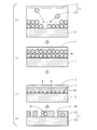
- the insulating electrodeposition coating 14 is electrodeposited on the surface of the electric wire 12 by using an electrodeposition coating apparatus 20 to form an insulating layer 18 (FIG. 1B).
- a cylindrical electric wire 22 (FIG. 2) having a circular cross section that is wound in a cylindrical shape is electrically connected to the positive electrode of the DC power supply 21 via the anode 23 in advance. And this cylindrical electric wire 22 is pulled up in the direction of the solid line arrow of FIG. 2, and passes through each process.
- a cylindrical electric wire 22 is flatly rolled by a pair of rolling rollers 24 to obtain a rectangular electric wire 12 having a rectangular cross section.
- the insulating electrodeposition paint 14 is stored in the electrodeposition tank 26 (FIGS. 1A and 2), and the rectangular electric wire is placed in the insulating electrodeposition paint 14 in the electrodeposition tank 26. 12 is passed.
- a cathode 27 electrically connected to the negative electrode of the DC power source 21 is inserted into the insulating electrodeposition coating 14 in the electrodeposition tank 26 so as to be spaced from the passing flat wire 12.
- a DC voltage is applied between the flat electric wire 12 and the insulating electrodeposition paint 14 by the DC power source 21. (Fig. 2).
- the polymer particles 16 dispersed in the solvent 17 of the insulating electrodeposition coating 14 are electrodeposited on the surface of the flat electric wire 12 to form an insulating layer 18 (FIGS. 1A and 1B).
- the temperature of the insulating electrodeposition coating 14 in the electrodeposition tank 26 is preferably 5 to 60 ° C., and the concentration of the polymer in the insulating electrodeposition coating 14 is preferably 1 to 40% by mass.
- the DC voltage of the DC power source 21 is preferably 1 to 300 V, and the DC current application time is preferably 0.01 to 30 seconds.
- the flat electric wire 12 having the insulating layer 18 electrodeposited on the surface thereof is dried as a pretreatment for the baking treatment, the solvent in the insulating layer 18 is evaporated, and the solvent in the insulating layer 18 is evaporated. Insulating layer 29 is obtained. Drying as a pretreatment is performed by a near infrared heating furnace.
- the rectangular electric wire 12 pulled up from the electrodeposition tank 26 is passed through the near-infrared heating furnace 28 (FIG. 2) to perform drying as a pretreatment.
- the peak wavelength of the near infrared heating furnace is preferably set in the range of 0.7 to 2.5 ⁇ m.
- Examples of the heating source in the near infrared heating furnace 28 include a halogen lamp heater and a tungsten heater.
- the pretreatment temperature is set lower than the temperature of the baking treatment described later. Further, the pretreatment temperature is preferably in the range of 50 to 200 ° C., and the pretreatment time is preferably in the range of 1 to 10 minutes.
- the temperature of pre-processing is the temperature of the center part in the near-infrared heating furnace measured with the thermocouple. The peak wavelength of the near-infrared heating furnace is more preferably set in the range of 1 to 2 ⁇ m, and the pretreatment temperature is more preferably in the range of 100 to 190 ° C., but is limited to this. There is no.
- the peak wavelength of the near-infrared heating furnace is limited to the range of 0.7 to 2.5 ⁇ m because the wire and the insulating layer cannot be sufficiently heated if the thickness is less than 0.7 ⁇ m, and the wire wavelength is more than 2.5 ⁇ m. Since the surface of the insulating layer is heated earlier to dry out from the surface of the insulating layer, the solvent in the insulating layer evaporates and foams, and voids or holes due to the foaming are formed in the cured insulating film. It is.
- the reason why the temperature of the pretreatment is set lower than the temperature of the baking treatment is based on the reason that foaming easily occurs when the temperature of the pretreatment is high.
- the reason why the pretreatment temperature is limited to the range of 50 to 200 ° C.
- the pretreatment time is limited to the range of 1 to 10 minutes because the insulating layer cannot be sufficiently dried if it is less than 1 minute, and the productivity is lowered if it exceeds 10 minutes.
- the electric wire 12 can be heated before the solvent 17 in 18 or the solvent 17 on the surface of the insulating layer 18 is heated.
- the solvent 17 in the insulating layer 18 evaporates sequentially from the portion in contact with the electric wire 12 toward the surface.
- FIG.1 (c) has shown the process in which a solvent evaporates by pre-processing.
- the insulating layer 29 dried by the pretreatment is baked to form the insulating film 13 on the surface of the wire 12 (FIG. 1 (d)).
- the electric wire 12 having the insulating layer 29 formed on the surface is passed through the baking furnace 31.
- the baking treatment is preferably performed by a near infrared heating furnace, a hot air heating furnace, an induction heating furnace, a far infrared heating furnace, or the like.
- the temperature of the baking treatment is preferably in the range of 200 to 500 ° C.
- the time of the baking treatment is preferably in the range of 1 to 10 minutes.
- the reason why the baking temperature is limited to the range of 200 to 500 ° C.
- the temperature of the baking treatment is the temperature of the central portion in the baking furnace.
- the baking temperature is more preferably in the range of 220 to 400 ° C., but is not limited thereto.
- FIG. 1 (d) voids and holes are not formed in the cured insulating film 13 after the baking treatment, and foaming due to evaporation of the solvent does not occur even if the insulating film 13 is thickened.
- the withstand voltage of the insulated wire 11 can be increased.
- the film thickness of the insulating film 13 can be increased to about 5 to 100 ⁇ m.
- FIG. 3C shows the evaporation process of the solvent when the baking process and the drying process are performed simultaneously.
- the solvent 17 in the insulating layer 18 evaporates, as shown in FIG. 3D, when the void 19a is formed inside the dry insulating layer 29 on the surface or when the void escapes to the surface.
- a hole 19b is formed in the insulating film 13 after curing. Therefore, foaming occurs when the insulating film 13 is thickened, and the withstand voltage of the insulated wire 11 cannot be increased.
- Example 1 a water-dispersed polyimide insulating electrodeposition paint containing 5% by mass of polyimide was stored in an electrodeposition tank.
- the average particle diameter of the polymer particles in this insulating electrodeposition paint was 0.4 ⁇ m.
- the temperature of the insulating electrodeposition paint in this electrodeposition tank was 25 ° C.
- a rectangular copper wire (electric wire) having a width of 2 mm and a thickness of 0.1 mm was used as an anode, and a stainless steel plate inserted into the insulating electrodeposition coating in the electrodeposition tank was used as a cathode.
- the flat copper wire was passed through the insulating electrodeposition paint in the electrodeposition tank at a line speed of 5 m / min.
- the polymer polyimide
- the time during which the flat copper wire was in contact with the insulating electrodeposition coating in the electrodeposition bath was 5 seconds.
- pretreatment was performed on a rectangular copper wire having an insulating layer formed on the surface. Specifically, pretreatment was performed by passing a rectangular copper wire having an insulating layer formed on the surface thereof through a near infrared heating furnace maintained at a temperature of 180 ° C.
- the solvent in the insulating layer formed on the surface of the rectangular copper wire evaporated.
- a halogen lamp heater was used as a heating source in the near infrared heating furnace.
- the peak wavelength of the halogen lamp heater was 1 ⁇ m.
- the temperature in a near-infrared heating furnace is the temperature of the center part in a furnace measured with the thermocouple.
- a baking treatment was performed on a rectangular copper wire having an insulating layer formed by evaporation of the solvent on the surface.
- a flat copper wire having an insulating layer with evaporated solvent formed on the surface thereof is baked by passing it through a baking furnace maintained at a temperature of 250 ° C., and the thickness of the insulating film is reduced.
- An insulated wire having a thickness of 20 ⁇ m was manufactured.
- a halogen lamp heater was used as a heating source in the baking furnace.
- the peak wavelength of the halogen lamp heater was 1 ⁇ m.
- the temperature in a baking furnace is the temperature of the center part in a furnace measured with the thermocouple.
- an insulated wire having an insulating film thickness of 30 ⁇ m was manufactured.
- the insulated wire whose thickness of an insulating film is 40 micrometers was manufactured by changing the voltage value at the time of letting a copper wire pass in the insulating electrodeposition coating material in an electrodeposition tank to 100V.
- These insulated wires were referred to as Example 1.
- Example 2 and Comparative Examples 1 to 5 As shown in Table 1, the insulated wires of Example 2 and Comparative Examples 1 to 5 were subjected to pretreatment heating source, pretreatment temperature, baking treatment heating source, baking treatment temperature, and pretreatment and baking treatment. By changing the order, the insulated wires having the insulating film thicknesses of 20 ⁇ m, 30 ⁇ m and 40 ⁇ m were manufactured. In addition, except having changed the heating source of pre-processing shown in Table 1, the temperature of pre-processing, the heating source of baking processing, the temperature of baking processing, the thickness of an insulating film, and the order of pre-processing and baking processing In the same manner as in Example 1, an insulated wire was manufactured.
- the thickness of the insulation film was Even when the thickness was increased to 40 ⁇ m, voids and holes were not formed in the insulating film, and it withstood an AC voltage of 10 kV.
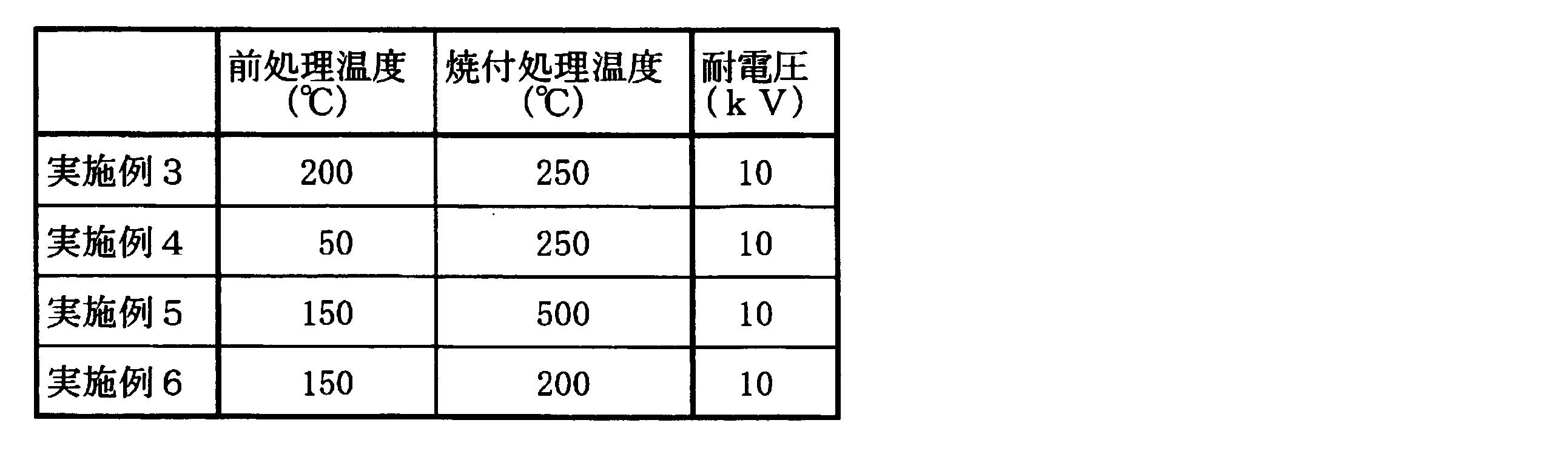
- Examples 3 to 6 As shown in Table 2, the insulated wires of Examples 3 to 6 were produced by changing the pretreatment temperature and the baking treatment temperature, respectively, and producing insulated wires having an insulation film thickness of 40 ⁇ m. In addition, the insulated wire whose thickness of an insulating film is 40 micrometers was manufactured like Example 1 except the pre-processing temperature shown in Table 2, and the baking process temperature.
- the insulated wires of Examples 3 to 6 withstood an AC voltage of 10 kV with no voids or holes formed in the insulating film.
- the method for manufacturing an insulated wire of the present invention can be used for a transformer, a reactor, a motor, etc. of an in-vehicle inverter.
- Insulating wire 11 Insulated wire 12 Flat rectangular wire (wire) 13 Insulating film 14 Insulating electrodeposition paint 17 Solvent 18, 29 Insulating layer
Landscapes
- Chemical & Material Sciences (AREA)
- Engineering & Computer Science (AREA)
- Materials Engineering (AREA)
- Organic Chemistry (AREA)
- Life Sciences & Earth Sciences (AREA)
- Chemical Kinetics & Catalysis (AREA)
- Wood Science & Technology (AREA)
- Manufacturing & Machinery (AREA)
- Electrochemistry (AREA)
- Metallurgy (AREA)
- Health & Medical Sciences (AREA)
- Molecular Biology (AREA)
- Thermal Sciences (AREA)
- Physics & Mathematics (AREA)
- Processes Specially Adapted For Manufacturing Cables (AREA)
- Insulated Conductors (AREA)
- Organic Insulating Materials (AREA)
- Paints Or Removers (AREA)
Abstract
Description
本願は、2015年2月13日に、日本に出願された特願2015-026041号に基づき優先権を主張し、その内容をここに援用する。
先ず、5質量%のポリイミドを含む水分散型ポリイミド絶縁電着塗料を電着槽に貯留した。この絶縁電着塗料中のポリマー粒子の平均粒子径は0.4μmであった。この電着槽内の絶縁電着塗料の温度は25℃であった。次いで、幅が2mm、厚さが0.1mmとなる平角状の銅線(電線)を陽極とし、上記電着槽内の絶縁電着塗料に挿入されたステンレス鋼板を陰極とした。平角状の銅線とステンレス鋼板との間に直流電圧50Vを印加した状態で、平角状の銅線を電着槽内の絶縁電着塗料中に5m/分の線速で通過させた。これにより平角状の銅線の表面にポリマー(ポリイミド)が電着されて絶縁層が形成された。平角状の銅線が電着槽内の絶縁電着塗料に接触している時間は5秒間であった。次に、表面に絶縁層が形成された平角状の銅線について前処理を行った。具体的には、表面に絶縁層が形成された平角状の銅線を、180℃の温度に保持された近赤外線加熱炉内に5m/分の線速で通過させることにより前処理を行った。これにより平角状の銅線の表面に形成された絶縁層中の溶媒が蒸発した。ここで、近赤外線加熱炉内の加熱源としてハロゲンランプヒータを用いた。ハロゲンランプヒータのピーク波長は1μmであった。また、近赤外線加熱炉内の温度は、熱電対で測定した炉内中央部の温度である。更に、溶媒が蒸発した絶縁層が表面に形成された平角状の銅線について焼付処理を行った。具体的には、溶媒が蒸発した絶縁層が表面に形成された平角状の銅線を、250℃の温度に保持された焼付炉を通過させることにより焼付処理を行い、絶縁皮膜の厚さが20μmである絶縁電線を製造した。ここで、焼付炉内の加熱源としてハロゲンランプヒータを用いた。ハロゲンランプヒータのピーク波長は1μmであった。また、焼付炉内の温度は、熱電対で測定した炉内中央部の温度である。更に、銅線を電着槽内の絶縁電着塗料中に通過させる際の電圧値を75Vに変更することにより、絶縁皮膜の厚さが30μmである絶縁電線を製造した。また、銅線を電着槽内の絶縁電着塗料中に通過させる際の電圧値を100Vに変更することにより、絶縁皮膜の厚さが40μmである絶縁電線を製造した。これらの絶縁電線を実施例1とした。
実施例2及び比較例1~5の絶縁電線は、表1に示すように前処理の加熱源、前処理の温度、焼付処理の加熱源、焼付処理の温度、並びに、前処理及び焼き付け処理の順序を変更して、絶縁皮膜の厚さが20μm、30μm及び40μmである絶縁電線をそれぞれ製造した。なお、表1に示した前処理の加熱源、前処理の温度、焼付処理の加熱源、焼付処理の温度、絶縁皮膜の厚さ、並びに、前処理及び焼き付け処理の順序を変更したこと以外は、実施例1と同様にして、絶縁電線を製造した。
実施例1及び2と比較例1~5の絶縁電線について、AC耐電圧試験機(菊水電子社製:TOS5000)により耐電圧をそれぞれ測定した。その結果を表1に示す。なお、表1において、膜厚は絶縁皮膜の厚さである。また、表1において、ボイド・穴とは、溶媒の蒸発により発泡して、絶縁皮膜中にボイドが形成された若しくは絶縁皮膜表面に穴が形成された状態をいい、耐電圧が測定不能であったことを示す。更に、表1において、焼付不足とは、ポリマーの熱硬化が不十分である状態をいう。

実施例3~6の絶縁電線は、表2に示すように前処理温度及び焼付処理温度を変更して、絶縁皮膜の厚さが40μmである絶縁電線をそれぞれ製造した。なお、表2に示した前処理温度及び焼付処理温度以外は、実施例1と同様にして、絶縁皮膜の厚さが40μmである絶縁電線を製造した。
実施例3~6の絶縁電線について、比較試験1と同様に、AC耐電圧試験機(菊水電子社製:TOS5000)により耐電圧をそれぞれ測定した。ここで、前処理の加熱源としてはハロゲンランプヒータを使用し、焼付処理の加熱源としては熱風炉を使用し、絶縁膜の厚さは40μmとした。その結果を表2に示す。
12 平角状の電線(電線)
13 絶縁皮膜
14 絶縁電着塗料
17 溶媒
18,29 絶縁層
Claims (3)
- ポリマーを含む絶縁電着塗料を用いて電着法により電線の表面に絶縁層を形成した後、焼付処理することにより、前記電線の表面に絶縁皮膜を形成する絶縁電線の製造方法において、
前記焼付処理の前に前記絶縁層中の溶媒を蒸発させる前処理を行い、
前記前処理が近赤外線加熱炉により行われ、
前記前処理の温度が前記焼付処理の温度より低い
ことを特徴とする絶縁電線の製造方法。 - 前記近赤外線加熱炉のピーク波長が0.7~2.5μmの範囲内に設定される請求項1記載の絶縁電線の製造方法。
- 前記前処理の温度が50~200℃の範囲内であり、前記焼付処理の温度が200~500℃の範囲内である請求項1記載の絶縁電線の製造方法。
Priority Applications (3)
| Application Number | Priority Date | Filing Date | Title |
|---|---|---|---|
| US15/544,159 US20180012684A1 (en) | 2015-02-13 | 2016-02-05 | Method for producing insulated electric wire |
| KR1020177017857A KR20170117376A (ko) | 2015-02-13 | 2016-02-05 | 절연 전선의 제조 방법 |
| CN201680005354.2A CN107112097A (zh) | 2015-02-13 | 2016-02-05 | 绝缘电线的制造方法 |
Applications Claiming Priority (2)
| Application Number | Priority Date | Filing Date | Title |
|---|---|---|---|
| JP2015026041A JP2016149281A (ja) | 2015-02-13 | 2015-02-13 | 絶縁電線の製造方法 |
| JP2015-026041 | 2015-02-13 |
Publications (1)
| Publication Number | Publication Date |
|---|---|
| WO2016129518A1 true WO2016129518A1 (ja) | 2016-08-18 |
Family
ID=56614329
Family Applications (1)
| Application Number | Title | Priority Date | Filing Date |
|---|---|---|---|
| PCT/JP2016/053489 Ceased WO2016129518A1 (ja) | 2015-02-13 | 2016-02-05 | 絶縁電線の製造方法 |
Country Status (5)
| Country | Link |
|---|---|
| US (1) | US20180012684A1 (ja) |
| JP (1) | JP2016149281A (ja) |
| KR (1) | KR20170117376A (ja) |
| CN (1) | CN107112097A (ja) |
| WO (1) | WO2016129518A1 (ja) |
Families Citing this family (1)
| Publication number | Priority date | Publication date | Assignee | Title |
|---|---|---|---|---|
| TW201930672A (zh) * | 2018-01-12 | 2019-08-01 | 智能紡織科技股份有限公司 | 導信紗及其製造方法 |
Citations (3)
| Publication number | Priority date | Publication date | Assignee | Title |
|---|---|---|---|---|
| JPS63257134A (ja) * | 1987-04-14 | 1988-10-25 | 日東電工株式会社 | 樹脂被覆伝送線状導体の製法 |
| JPH03241609A (ja) * | 1990-02-20 | 1991-10-28 | Mitsubishi Cable Ind Ltd | 平角状超薄膜絶縁電線 |
| JP2016031867A (ja) * | 2014-07-29 | 2016-03-07 | 日立金属株式会社 | エナメル線の製造方法及び製造装置 |
Family Cites Families (3)
| Publication number | Priority date | Publication date | Assignee | Title |
|---|---|---|---|---|
| JPH10289625A (ja) * | 1997-04-16 | 1998-10-27 | Hitachi Cable Ltd | エナメル線焼付炉 |
| JP2010140641A (ja) * | 2008-12-09 | 2010-06-24 | Mitsubishi Cable Ind Ltd | 絶縁電線の製造方法 |
| CN102938277A (zh) * | 2012-11-26 | 2013-02-20 | 苏州市新的电工有限公司 | 一种带远红外辅助加热装置的漆包线烘烤炉 |
-
2015
- 2015-02-13 JP JP2015026041A patent/JP2016149281A/ja active Pending
-
2016
- 2016-02-05 WO PCT/JP2016/053489 patent/WO2016129518A1/ja not_active Ceased
- 2016-02-05 US US15/544,159 patent/US20180012684A1/en not_active Abandoned
- 2016-02-05 CN CN201680005354.2A patent/CN107112097A/zh not_active Withdrawn
- 2016-02-05 KR KR1020177017857A patent/KR20170117376A/ko not_active Withdrawn
Patent Citations (3)
| Publication number | Priority date | Publication date | Assignee | Title |
|---|---|---|---|---|
| JPS63257134A (ja) * | 1987-04-14 | 1988-10-25 | 日東電工株式会社 | 樹脂被覆伝送線状導体の製法 |
| JPH03241609A (ja) * | 1990-02-20 | 1991-10-28 | Mitsubishi Cable Ind Ltd | 平角状超薄膜絶縁電線 |
| JP2016031867A (ja) * | 2014-07-29 | 2016-03-07 | 日立金属株式会社 | エナメル線の製造方法及び製造装置 |
Non-Patent Citations (1)
| Title |
|---|
| YUKIO UESHIMA: "Halogen Heater o Mochiita Sekigaisen Kanetsu no Tokucho to Kanetsu Jirei", LIGHT EDGE, June 2013 (2013-06-01), pages 10 - 19 * |
Also Published As
| Publication number | Publication date |
|---|---|
| JP2016149281A (ja) | 2016-08-18 |
| KR20170117376A (ko) | 2017-10-23 |
| CN107112097A (zh) | 2017-08-29 |
| US20180012684A1 (en) | 2018-01-11 |
Similar Documents
| Publication | Publication Date | Title |
|---|---|---|
| JP6973576B2 (ja) | 水分散型絶縁皮膜形成用電着液 | |
| KR102676821B1 (ko) | 전착액 및 전착 도장체 | |
| US11581127B2 (en) | Insulated electric wire, production method therefor, coil and coil production method using same | |
| TW201835246A (zh) | 電鍍液及使用此電鍍液之附絕緣被膜之導體的製造方法 | |
| JPWO2013157574A1 (ja) | 自己析出型銅用表面処理剤および樹脂皮膜付き銅含有基材の製造方法 | |
| WO2016129518A1 (ja) | 絶縁電線の製造方法 | |
| US10395798B2 (en) | Heat-resistant insulated wire and electrodeposition liquid used to form insulating layer therefor | |
| JP6069035B2 (ja) | 電着塗装体の製造方法 | |
| JP6412740B2 (ja) | 電着塗装体の製造方法 | |
| US10984922B2 (en) | Insulated electric wire, method for manufacturing same, and coil | |
| JP2017137541A (ja) | 電着液及びこれを用いた絶縁皮膜の形成方法 | |
| CN107075154A (zh) | 通过气‑液界面等离子体聚合制备聚合物薄膜的方法及从中制备的聚合物薄膜 | |
| JP2023032641A (ja) | 絶縁性アルミニウム合金導体及びその製造方法 | |
| JP2017066014A (ja) | 樹脂コート窒化ホウ素粉末及びその分散液 | |
| JP6708192B2 (ja) | 絶縁電線の製造方法 | |
| KR101649671B1 (ko) | 수지피복 금속판 및 그 제조방법 | |
| JP6008028B1 (ja) | ポリイミド管状体の製造方法 | |
| JP7524567B2 (ja) | 絶縁皮膜付き打ち抜き加工品及びその製造方法 | |
| JP2008276963A (ja) | 絶縁電線 | |
| JP2023032642A (ja) | 絶縁導体の製造方法、電着装置及び絶縁導体製造装置 | |
| JP2022023932A (ja) | エナメル線 |
Legal Events
| Date | Code | Title | Description |
|---|---|---|---|
| 121 | Ep: the epo has been informed by wipo that ep was designated in this application |
Ref document number: 16749162 Country of ref document: EP Kind code of ref document: A1 |
|
| ENP | Entry into the national phase |
Ref document number: 20177017857 Country of ref document: KR Kind code of ref document: A |
|
| WWE | Wipo information: entry into national phase |
Ref document number: 15544159 Country of ref document: US |
|
| NENP | Non-entry into the national phase |
Ref country code: DE |
|
| 122 | Ep: pct application non-entry in european phase |
Ref document number: 16749162 Country of ref document: EP Kind code of ref document: A1 |