WO2016121188A1 - 太陽電池モジュール及び太陽電池モジュールの製造方法 - Google Patents
太陽電池モジュール及び太陽電池モジュールの製造方法 Download PDFInfo
- Publication number
- WO2016121188A1 WO2016121188A1 PCT/JP2015/081545 JP2015081545W WO2016121188A1 WO 2016121188 A1 WO2016121188 A1 WO 2016121188A1 JP 2015081545 W JP2015081545 W JP 2015081545W WO 2016121188 A1 WO2016121188 A1 WO 2016121188A1
- Authority
- WO
- WIPO (PCT)
- Prior art keywords
- solar cell
- eva
- silicone
- light
- cell module
- Prior art date
- Legal status (The legal status is an assumption and is not a legal conclusion. Google has not performed a legal analysis and makes no representation as to the accuracy of the status listed.)
- Ceased
Links
Images





Classifications
-
- H—ELECTRICITY
- H10—SEMICONDUCTOR DEVICES; ELECTRIC SOLID-STATE DEVICES NOT OTHERWISE PROVIDED FOR
- H10F—INORGANIC SEMICONDUCTOR DEVICES SENSITIVE TO INFRARED RADIATION, LIGHT, ELECTROMAGNETIC RADIATION OF SHORTER WAVELENGTH OR CORPUSCULAR RADIATION
- H10F19/00—Integrated devices, or assemblies of multiple devices, comprising at least one photovoltaic cell covered by group H10F10/00, e.g. photovoltaic modules
- H10F19/80—Encapsulations or containers for integrated devices, or assemblies of multiple devices, having photovoltaic cells
- H10F19/804—Materials of encapsulations
-
- H—ELECTRICITY
- H10—SEMICONDUCTOR DEVICES; ELECTRIC SOLID-STATE DEVICES NOT OTHERWISE PROVIDED FOR
- H10F—INORGANIC SEMICONDUCTOR DEVICES SENSITIVE TO INFRARED RADIATION, LIGHT, ELECTROMAGNETIC RADIATION OF SHORTER WAVELENGTH OR CORPUSCULAR RADIATION
- H10F19/00—Integrated devices, or assemblies of multiple devices, comprising at least one photovoltaic cell covered by group H10F10/00, e.g. photovoltaic modules
- H10F19/80—Encapsulations or containers for integrated devices, or assemblies of multiple devices, having photovoltaic cells
-
- H—ELECTRICITY
- H10—SEMICONDUCTOR DEVICES; ELECTRIC SOLID-STATE DEVICES NOT OTHERWISE PROVIDED FOR
- H10F—INORGANIC SEMICONDUCTOR DEVICES SENSITIVE TO INFRARED RADIATION, LIGHT, ELECTROMAGNETIC RADIATION OF SHORTER WAVELENGTH OR CORPUSCULAR RADIATION
- H10F71/00—Manufacture or treatment of devices covered by this subclass
-
- Y—GENERAL TAGGING OF NEW TECHNOLOGICAL DEVELOPMENTS; GENERAL TAGGING OF CROSS-SECTIONAL TECHNOLOGIES SPANNING OVER SEVERAL SECTIONS OF THE IPC; TECHNICAL SUBJECTS COVERED BY FORMER USPC CROSS-REFERENCE ART COLLECTIONS [XRACs] AND DIGESTS
- Y02—TECHNOLOGIES OR APPLICATIONS FOR MITIGATION OR ADAPTATION AGAINST CLIMATE CHANGE
- Y02E—REDUCTION OF GREENHOUSE GAS [GHG] EMISSIONS, RELATED TO ENERGY GENERATION, TRANSMISSION OR DISTRIBUTION
- Y02E10/00—Energy generation through renewable energy sources
- Y02E10/50—Photovoltaic [PV] energy
-
- Y—GENERAL TAGGING OF NEW TECHNOLOGICAL DEVELOPMENTS; GENERAL TAGGING OF CROSS-SECTIONAL TECHNOLOGIES SPANNING OVER SEVERAL SECTIONS OF THE IPC; TECHNICAL SUBJECTS COVERED BY FORMER USPC CROSS-REFERENCE ART COLLECTIONS [XRACs] AND DIGESTS
- Y02—TECHNOLOGIES OR APPLICATIONS FOR MITIGATION OR ADAPTATION AGAINST CLIMATE CHANGE
- Y02P—CLIMATE CHANGE MITIGATION TECHNOLOGIES IN THE PRODUCTION OR PROCESSING OF GOODS
- Y02P70/00—Climate change mitigation technologies in the production process for final industrial or consumer products
- Y02P70/50—Manufacturing or production processes characterised by the final manufactured product
Definitions
- the present invention relates to a solar cell module and a manufacturing method thereof.
- a crystalline solar cell module formed by connecting solar cell elements made of a semiconductor substrate such as silicon has a light-transmitting substrate such as glass on the light-receiving surface side and a light-transmitting substrate such as glass or PET film on the back side.
- EVA is widely used as a sealing material that has a back surface protective material such as the like and exists between them.
- Non-patent Document 1 As a measure for improving such a problem, there is an improvement of a light-receiving surface antireflection film of a solar battery cell (Patent Document 1).
- the improvement of the light-receiving surface antireflection film has problems such as a slight decrease in the output of the solar battery cell and the improvement in facilities in the process of forming the solar battery cell antireflection film.
- Non-patent Document 1 an ionomer is mentioned as a sealing material which has PID tolerance, an ionomer has a problem that cost is high and raises the solar cell module production cost.
- Non-Patent Document 2 A solar cell module having a structure sealed with a laminate of ionomer and EVA has also been proposed (Non-Patent Document 2).
- the ionomer can prevent Na + diffusion from the light-receiving surface glass and suppress the generation of PID.
- a method of inserting a transparent PET resin film sheet between EVA and ionomer has been proposed (Patent Document 2). In this method, lamination must be performed by laminating three layers of ionomer, PET resin film, and EVA between the glass and the cell, and the process is complicated.
- Non-patent Document 1 silicone is mentioned as a sealing material which does not produce PID. It has been reported that PID phenomenon hardly occurs in a solar cell module using silicone as a sealing material (Non-patent Document 1). However, in general, silicone is a liquid, so that it is necessary to introduce new equipment to introduce it into the solar cell module process, and there is a problem that the material cost is high and the manufacturing cost of the solar cell module increases. .
- the present invention has been made to solve the above-described problems, and provides a solar cell module that is easy in the solar cell module process and that has good laminate sealing and is excellent in PID resistance, and a method for manufacturing the solar cell module. Objective.
- the inventors of the present invention have laminated EVA and silicone to seal solar cell element strings (a plurality of solar cell elements and a connecting body connecting these solar cell elements). It has been found that using the body is effective.
- this invention provides the following solar cell module and its manufacturing method.
- a solar cell module having a light transmissive substrate on the light receiving surface side and a back surface protective material on the back surface side, and EVA (ethylene) as a sealing material between the light receiving surface side light transmissive substrate and the solar cell element
- EVA ethylene
- a solar cell module having a structure in which a vinyl acetate copolymer) and silicone are adjacent and laminated, and a solar cell element and a back surface protective material are sealed with EVA.
- a solar cell module having a light transmissive substrate on the light receiving surface side and a back surface protective material on the back surface side, and EVA (ethylene) as a sealing material between the light receiving surface side light transmissive substrate and the solar cell element (Vinyl acetate copolymer) and silicone are adjacent and laminated, and EVA (ethylene vinyl acetate copolymer) and silicone are adjacently laminated between the back surface protective material and the solar cell element.
- a solar cell module having a structure.
- the EVA is in contact with the light-receiving surface side light-transmitting substrate, the silicone adjacent thereto is in contact with the solar cell element light-receiving surface, the silicone is in contact with the back surface protective material, and the EVA adjacent thereto is in contact with the back surface of the solar cell element.
- Silicone is in contact with the light-receiving surface side light-transmitting substrate, EVA adjacent to this is in contact with the solar cell element light-receiving surface, EVA is in contact with the back surface protective material, and silicone adjacent thereto is in contact with the back surface of the solar cell element.
- the solar cell module according to [2].
- the EVA and silicone form a composite laminate in which EVA and silicone are stacked in a two-layer structure, the thickness of the silicone is 0.05 to 3 mm, and the thickness of the composite laminate is 0.45 to 3.6 mm.
- the solar cell module according to any one of [1] to [8], wherein [10]
- the silicone is (A) The following average composition formula (I) R 1 a SiO (4-a) / 2 (I) (In the formula, R 1 represents the same or different unsubstituted or substituted monovalent hydrocarbon group, and a is a positive number of 1.95 to 2.05.) 100 parts by mass of an organopolysiloxane having a degree of polymerization represented by (B) 20 to 150 parts by mass of reinforcing silica having a specific surface area of 50 m 2 / g or more, (C) Curing agent The solar cell module according to any one of [1] to [9], which is a cured product of a silicone composition containing an effective amount for cu
- the solar cell module according to any one of [1] to [10], wherein a back light transmissive substrate is used as a back surface protective material.
- the solar cell module has a light-transmitting substrate on the light-receiving surface side, and a stacked body in which EVA and an unvulcanized silicone composition are stacked in a two-layer structure is placed on the light-transmitting substrate, and the stacked body
- a solar cell element string is placed on the upper part, and an EVA single layer or a laminate in which EVA and an unvulcanized silicone composition are stacked in a two-layer structure is placed on the back surface of the solar cell element string, and the rearmost surface
- After laminating the back surface protective material on the side it is heated and pressed under vacuum using a vacuum laminator, and the unvulcanized silicone composition and EVA are crosslinked to form a module [1] to [ 11]
- the manufacturing method of the solar cell module in any one of.
- the solar cell module of the present invention is not significantly changed in the manufacturing process of the solar cell module, can be easily manufactured using a vacuum laminator, has extremely high resistance to the PID phenomenon, and is associated with the PID phenomenon. The output drop is suppressed.
- the solar cell module according to the present invention has a light transmissive substrate on the light receiving surface side, a back surface protective material on the back surface side, a plurality of solar cell elements and the plurality of solar cells between the light receiving surface and the back surface.
- a solar cell element string composed of a connecting body for connecting the battery element is disposed, and a front side sealing agent for sealing the string is filled between the light transmissive substrate and the solar cell element string, and a back surface protective material is provided.
- a back side sealing agent is filled between the solar cell element strings.
- the solar cell element can be applied to a P-type semiconductor substrate, an N-type semiconductor substrate, and a thin-film element, and the effect is exhibited in all cases.
- white plate glass polycarbonate, acrylic plate, or the like is used as the light transmissive substrate.
- soda lime glass is generally used as the white plate glass. Soda lime glass is likely to generate Na + ions, and when it is systemized, when many solar cell modules are connected in series, when a high voltage (minus) load is generated on the cell side, Na on the cell side + Ions move, reach the cell surface, cause recombination, and decrease the output of the solar cell module, but the present invention has high resistance to the PID phenomenon, and can suppress the decrease in output of the solar cell module due to the PID phenomenon Therefore, white plate glass can be used effectively.
- TPT polyvinyl fluoride
- adhesive / PET polyethylene terephthalate
- PVF polyethylene terephthalate
- PVF polyvinyl fluoride
- PET polyethylene terephthalate
- PVF polyvinyl fluoride
- EVA polyethylene terephthalate
- a film of a laminate shown in “/ adhesive / PET” is used.
- the same light-transmitting substrate as that on the front surface side can be used.
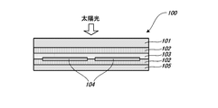
- FIG. 1 shows a solar cell module 100 according to the first embodiment of the present invention.
- FIG. 2 shows a solar cell module 200 according to the second embodiment of the present invention. From the sunlight incident direction, white glass, a sealing material silicone 103, EVA 102, and a crystalline silicon solar cell element are used as the light transmissive substrate 101. The strings 104, the sealing material EVA102, and the back surface protective material 105 are configured in this order.
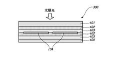
- FIG. 3 shows a solar cell module 300 according to the third embodiment of the present invention. From the sunlight incident direction, white glass, sealing material EVA102, silicone 103, and crystalline silicon solar cell element string 104 are used as the light transmissive substrate 101. The sealing material EVA102, the silicone 103, and the back surface protective material 105 are configured in this order.
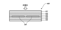
- FIG. 4 shows a solar cell module 400 according to the fourth embodiment of the present invention. From a sunlight incident direction, white glass, a sealing material silicone 103, EVA 102, and a crystalline silicon solar cell element string 104 are used as a light transmissive substrate 101.
- the sealing material EVA102, the silicone 103, and the back surface protective material 105 are configured in this order.
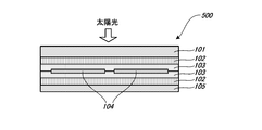
- FIG. 5 shows a solar cell module 500 according to the fifth embodiment of the present invention. From the sunlight incident direction, white glass, sealing material EVA102, silicone 103, and crystalline silicon solar cell element string 104 are used as the light transmissive substrate 101.
- the sealing material silicone 103, the EVA 102, and the back surface protective material 105 are configured in this order.
- FIG. 6 shows a solar cell module 600 according to the sixth embodiment of the present invention. From the sunlight incident direction, white glass, a sealing material silicone 103, EVA 102, and a crystalline silicon solar cell element string 104 are used as the light transmissive substrate 101.
- the sealing material silicone 103, the EVA 102, and the back surface protective material 105 are configured in this order.
- the thickness of silicone is preferably 0.05 to 3 mm, particularly preferably 0.1 to 1 mm, and the thickness of EVA is preferably 0.4 to 0.6 mm.
- the thickness of the composite laminate is preferably 0.45 to 3.6 mm, particularly preferably 0.5 to 1.6 mm.
- the thickness is preferably 0.4 to 0.6 mm.
- EVA ethylene vinyl acetate copolymer
- those usually used for solar cell modules can be used, and commercially available products can be used.
- a copolymer obtained by copolymerizing ethylene and vinyl acetate in a mass ratio of 75:25 to 65:35 is commercially available.
- the silicone is preferably obtained by curing a silicone composition containing the following components (A) to (C).
- R 1 represents the same or different unsubstituted or substituted monovalent hydrocarbon group, and a is a positive number of 1.95 to 2.05.
- the component (A) is an organopolysiloxane having a degree of polymerization represented by the following average composition formula (I) of 100 or more.
- R 1 a SiO (4-a) / 2 (I) (In the formula, R 1 represents the same or different unsubstituted or substituted monovalent hydrocarbon group, and a is a positive number of 1.95 to 2.05.)
- R 1 represents the same or different unsubstituted or substituted monovalent hydrocarbon group, usually having 1 to 12 carbon atoms, particularly preferably having 1 to 8 carbon atoms.
- alkyl groups such as methyl, ethyl, propyl, butyl, hexyl and octyl, cycloalkyl such as cyclopentyl and cyclohexyl, alkenyl such as vinyl, allyl and propenyl, cyclo
- An aryl group such as an alkenyl group, a phenyl group or a tolyl group, an aralkyl group such as a benzyl group or a 2-phenylethyl group, or a group in which some or all of the hydrogen atoms of these groups are substituted with a halogen atom or a cyano group
- the main chain of the organopolysiloxane is composed of repeating dimethylsiloxane units, or a part of the dimethylpolysiloxane structure composed of repeating dimethylsiloxane units constituting the main chain is phenyl group, vinyl group, A diphenylsiloxane unit having a 3,3,3-trifluoropropyl group, a methylphenylsiloxane unit, a methylvinylsiloxane unit, a methyl-3,3,3-trifluoropropylsiloxane unit, or the like is suitable. .
- the organopolysiloxane preferably has two or more aliphatic unsaturated groups such as alkenyl groups and cycloalkenyl groups in one molecule, and particularly preferably a vinyl group.
- the aliphatic unsaturated group may be bonded to a silicon atom at the molecular chain end, or may be bonded to a silicon atom in the middle of the molecular chain, or both. It is preferably bonded to the silicon atom.
- A is a positive number of 1.95 to 2.05, preferably 1.98 to 2.02, more preferably 1.99 to 2.01.
- the organopolysiloxane of component (A) is blocked with a triorganosiloxy group such as a trimethylsiloxy group, a dimethylphenylsiloxy group, a dimethylhydroxysiloxy group, a dimethylvinylsiloxy group, a methyldivinylsiloxy group, or a trivinylsiloxy group.
- a triorganosiloxy group such as a trimethylsiloxy group, a dimethylphenylsiloxy group, a dimethylhydroxysiloxy group, a dimethylvinylsiloxy group, a methyldivinylsiloxy group, or a trivinylsiloxy group.
- Preferred examples can be given.
- Particularly preferred are methyl vinyl polysiloxane, methyl phenyl vinyl polysiloxane, methyl trifluoropropyl vinyl polysiloxane and the like.
- Such an organopolysiloxane can be obtained by, for example, hydrolyzing and condensing one or more types of organohalogenosilanes, or by converting cyclic polysiloxanes (siloxane trimers, tetramers, etc.) to alkaline or acidic. It can obtain by ring-opening polymerization using the catalyst of.
- These are basically linear diorganopolysiloxanes, but the component (A) may be a mixture of two or more different molecular weights (degree of polymerization) and molecular structures.
- the degree of polymerization of the organopolysiloxane is 100 or more, preferably 100 to 100,000, particularly preferably 3,000 to 20,000. This degree of polymerization can be measured as a weight average degree of polymerization in terms of polystyrene by gel permeation chromatography (GPC) analysis.
- GPC gel permeation chromatography
- the reinforcing silica having a BET specific surface area of 50 m 2 / g or more as the component (B) is added to obtain a composition having excellent mechanical strength before and after curing.
- the BET specific surface area is preferably more than 200 m 2 / g, more preferably 250 m 2 / g or more.
- the transparency of the cured product may be lowered.
- the upper limit is not particularly limited, but is usually 500 m 2 / g or less.
- the reinforcing silica as the component (B) examples include fumed silica (dry silica or fumed silica), precipitated silica (wet silica), and the like. Further, those whose surfaces have been subjected to a hydrophobic treatment with chlorosilane, alkoxysilane, hexamethyldisilazane, or the like are also preferably used. In particular, the treatment with hexamethyldisilazane is preferable because of high transparency. In order to improve transparency, it is preferable to use fumed silica as reinforcing silica. Reinforcing silica may be used alone or in combination of two or more.
- component (B) As the reinforcing silica of component (B), commercially available products can be used.
- Aerosil series such as Aerosil 130, Aerosil 200, Aerosil 300, Aerosil R-812, Aerosil R-972, Aerosil R-974 (Japan)
- Aerosil Co., Ltd. Cabosil MS-5, MS-7 (Cabot Co., Ltd.), Leorosil QS-102, 103, MT-10 (Tokuyama Co., Ltd.), etc.
- Untreated or surface such as fumed silica (that is, hydrophilic or hydrophobic), Toxeal US-F (manufactured by Tokuyama Corporation), NIPSIL-SS, NIPSIL-LP (manufactured by Nippon Silica Industry Co., Ltd.) Examples include hydrophobized precipitated silica.
- the blending amount of the reinforcing silica of the component (B) is 20 to 150 parts by weight, preferably 30 to 90 parts by weight, more preferably 50 to 50 parts by weight with respect to 100 parts by weight of the organopolysiloxane of the component (A). 90 parts by mass.
- the blending amount of the component (B) is too small, the reinforcing effect before and after curing cannot be obtained, and the transparency of the silicone sealing material after curing is lowered.
- the amount is too large, it is difficult to disperse the silica in the silicone sealing material, and at the same time, the processability into a sheet may be deteriorated.
- the curing agent for component (C) is not particularly limited as long as it can cure component (A), but (a) addition reaction (hydrosilylation reaction) type curing agent widely known as a curing agent for silicone compositions. That is, a combination of an organohydrogenpolysiloxane (crosslinking agent) and a hydrosilylation reaction catalyst, or (b) an organic peroxide is preferable.
- the organohydrogenpolysiloxane as a crosslinking agent in the above contains hydrogen atoms (SiH groups) bonded to at least two silicon atoms in one molecule.
- Specific examples include a methyl group, an ethyl group, Alkyl groups such as propyl group, butyl group, pentyl group and hexyl group, unsubstituted monovalent hydrocarbon groups such as cyclohexyl group, cyclohexenyl group and phenyl group, 3,3,3-trifluoropropyl group, cyanomethyl group, etc.
- a substituted monovalent hydrocarbon group such as a substituted alkyl group in which at least a part of hydrogen atoms of the monovalent hydrocarbon group is substituted with a halogen atom or a cyano group, b is 0.7 to 2.1, c Is 0.01 to 1.0, and b + c is 0.8 to 3.0, preferably b is 0.8 to 2.0, c is 0.2 to 1.0, and b + c is 1.0 to 2.
- a conventionally known organohydrogenpolysiloxane represented by the formula is applicable. Further, the molecular structure of the organohydrogenpolysiloxane may be any of linear, cyclic, branched, and three-dimensional network structures.
- the number of silicon atoms in one molecule is preferably 2 to 300, particularly about 4 to 200, which is liquid at room temperature.
- the hydrogen atom (SiH group) bonded to the silicon atom may be at the end of the molecular chain, at the side chain, or both, and at least two (usually 2 to 300) per molecule.
- those containing 3 or more (for example, 3 to 200), more preferably about 4 to 150 are used.
- organohydrogenpolysiloxane examples include 1,1,3,3-tetramethyldisiloxane, 1,3,5,7-tetramethylcyclotetrasiloxane, methylhydrogencyclopolysiloxane, and methylhydrogen.
- Siloxane / dimethylsiloxane cyclic copolymer tris (dimethylhydrogensiloxy) methylsilane, tris (dimethylhydrogensiloxy) phenylsilane, trimethylsiloxy group-capped methylhydrogenpolysiloxane, both ends trimethylsiloxy group-capped dimethylsiloxane methyl Hydrogensiloxane copolymer, dimethylhydrogensiloxy group-capped dimethylpolysiloxane at both ends, dimethylhydrogensiloxy group-capped dimethylsiloxane methylhydride at both ends Gensiloxane copolymer, trimethylsiloxy group-capped methylhydrogensiloxane / diphenylsiloxane copolymer, trimethylsiloxy group-capped methylhydrogensiloxane / diphenylsiloxane / dimethylsiloxane copolymer, cyclic methylhydrogenpolysilox
- the compounding amount of the organohydrogenpolysiloxane is 0.1 to 30 parts by mass, more preferably 0.1 to 10 parts by mass, and still more preferably 0.3 to 100 parts by mass of the organopolysiloxane of the component (A). It is preferable that the amount be 10 parts by mass.
- the organohydrogenpolysiloxane has a molar ratio of hydrogen atoms bonded to silicon atoms in the component (C) (that is, SiH groups) to alkenyl groups bonded to silicon atoms in the component (A) is 0.5. It is preferable to add in an amount of -5 mol / mol, preferably 0.8-4 mol / mol, more preferably 1-3 mol / mol.
- hydrosilylation reaction catalyst used in the crosslinking reaction of the above (a) addition reaction can be applied, for example, platinum black, platinum chloride, chloroplatinic acid, platinum chloride.
- platinum black platinum black
- platinum chloride chloroplatinic acid
- platinum chloride examples thereof include a reaction product of an acid and a monohydric alcohol, a complex of chloroplatinic acid and an olefin, a platinum-based catalyst such as platinum bisacetoacetate, a palladium-based catalyst, and a rhodium-based catalyst.
- the blending amount of the hydrosilylation reaction catalyst can be a catalytic amount, and is usually preferably 1 to 1,000 ppm, more preferably 5 to 100 ppm in terms of platinum group metal mass. If it is less than 1 ppm, the addition reaction may not proceed sufficiently and the curing may be insufficient, and it is uneconomical to add more than 1,000 ppm.
- an addition reaction control agent may be used for the purpose of adjusting the curing rate or pot life.
- Specific examples include ethynylcyclohexanol and tetramethyltetravinylcyclotetrasiloxane.
- examples of (b) organic peroxides include benzoyl peroxide, 2,4-dichlorobenzoyl peroxide, p-methylbenzoyl peroxide, o-methylbenzoyl peroxide, 2,4-dicumyl peroxide, 2,5-dimethyl-bis (2,5-t-butylperoxy) hexane, di-t-butylperoxide, t-butylperbenzoate, 1,6-hexanediol-bis-t-butylperoxycarbonate, etc. Is mentioned.
- the amount of (b) organic peroxide added is preferably 0.1 to 15 parts by mass, particularly preferably 0.2 to 10 parts by mass with respect to 100 parts by mass of component (A). If the addition amount is too small, the crosslinking reaction may not proceed sufficiently, resulting in a decrease in hardness and insufficient strength. May increase discoloration.
- a flame retardant imparting agent, a colorant, and an adhesion imparting agent such as a carbon functional silane having an alkoxysilyl group are added as long as the object of the present invention is not impaired. can do.
- the silicone composition according to the present invention can be obtained by kneading a predetermined amount of the above-described components with a two-roll, kneader, Banbury mixer or the like.
- the plasticity before curing of the silicone composition thus prepared is 150 to 1,000, preferably 200 to 800, more preferably 250 to 600. If the plasticity is less than 150, it is difficult to maintain the shape of the uncured sheet, and the tack is strong and difficult to use. On the other hand, if it exceeds 1,000, the sheet forming process becomes difficult.
- the plasticity can be measured according to JIS K 6249.
- the molding method is not particularly limited, and extrusion molding, calendar molding, and the like are used.
- the thickness of the silicone composition sheet is preferably 0.05 to 3 mm.
- the unvulcanized silicone composition according to the present invention can be molded while using EVA as a base material and bonding one surface of the silicone composition to EVA.
- both the laminated sheets are press-molded with a roll at the same time or press-molded with a roll with a single layer of silicone, There is a method of pasting and molding while laminating simultaneously with EVA.
- the silicone composition can be cured by heating at 120 to 150 ° C. for 20 to 60 minutes.
- the solar cell module has a light-transmitting substrate on the light-receiving surface side, and EVA and an unvulcanized silicone composition overlap each other in a two-layer structure.
- the laminated body is placed on a light-transmitting substrate, a solar cell element string is placed on the upper part of the laminated body, and an EVA single layer or EVA and an unvulcanized silicone composition on the back surface of the solar cell element string After laminating a laminate with a two-layer structure and laminating a back protective material on the backmost side, it is heated and pressed under vacuum using a vacuum laminator to crosslink the unvulcanized silicone composition and EVA Can be modularized.
- the part of the unit of a compounding quantity is a mass part.
- a weight average molecular weight and a weight average polymerization degree are the polystyrene conversion values in a gel permeation chromatography (GPC) analysis.
- Examples and Comparative Examples First, the silicone used in Examples and Comparative Examples will be described. 100 parts of an organopolysiloxane comprising 99.85 mol% of dimethylsiloxane units, 0.025 mol% of methylvinylsiloxane units and 0.125 mol% of dimethylvinylsiloxane units and having an average degree of polymerization of about 6,000, BET specific surface area 70 parts of 300 m 2 / g silica (trade name Aerosil 300, manufactured by Nippon Aerosil Co., Ltd.), 16 parts of hexamethyldisilazane as a dispersant and 4 parts of water were added, and the mixture was kneaded with a kneader at 170 ° C. A compound was prepared by heat treatment for 2 hours.
- an organopolysiloxane comprising 99.85 mol% of dimethylsiloxane units, 0.025 mol% of methylvinylsiloxane
- EVA sheet for solar cells (fast cure type) manufactured by Sunvic Co., Ltd. is used as EVA, and white glass (3.2 mm thickness, with single-sided embossed shape) manufactured by Nakajima Glass Industry Co., Ltd. as the light-transmitting substrate on the surface.
- TPT Tedlar-PET-Tedlar: PTD250
- AM Packaging Co., Ltd. was used as a back surface protective material, and solar cell modules of Examples and Comparative Examples were produced. That is, solar cell modules 100 to 600 of Examples 1 to 6 were obtained according to the configuration of FIGS. Moreover, the solar cell module 700 (Comparative Example 1) shown in FIG. 7 was obtained.
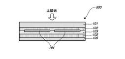
- FIG. 8 shows a solar cell module 800 (Comparative Example 2). From the sunlight incident direction, white glass, a sealing material EVA102, a crystalline silicon solar cell element string 104, a sealing material silicone 103, EVA102, The back surface protective material 105 is configured in this order.
- FIG. 9 shows a solar cell module 900 (Comparative Example 3). From the sunlight incident direction, white glass, a sealing material EVA102, a crystalline silicon solar cell element string 104, a sealing material EVA102, and a back surface protection material are used as the light transmissive substrate 101. The order is 105.
- FIG. 10 shows a solar cell module 1000 (Comparative Example 4). From the sunlight incident direction, white glass, a sealing material silicone 103, a crystalline silicon solar cell element string 104, a sealing material silicone 103, and a back surface as a light transmissive substrate 101.
- the protective material 105 is configured in this order.
- the sealing material EVA102 has a thickness of 0.45 mm and is in the form of a sheet.
- the sealing material silicone 103 has a thickness of 0.5 mm, and the solar cell modules 100 to 700 have a sheet shape in which the silicone 103 is integrated with the EVA 102. That is, the total thickness of the EVA silicone laminate is 0.95 mm.
- the sealing material silicone 103 has a thickness of 0.5 mm alone.
- the solar cell module 100 is made of six types of unvulcanized encapsulant silicone 103 having thicknesses of 0.05, 0.1, 0.25, 0.5, 1 and 3 mm, and integrated with EVA 102, respectively. Made it. Therefore, the thickness of the sealing material EVA silicone laminate is 0.5, 0.55, 0.7, 0.95, 1.45, and 3.45 mm, respectively.
- the solar cell strings 104 were arranged in 4 straight sizes (2 ⁇ 2 columns), and the connection wirings were respectively connected in series and formed.
- the solar cell module 100 will be described as an example.
- the EVA silicone composite (102, 103) was placed on the upper surface of the white plate glass (light transmissive substrate 101) so that the EVA 102 was oriented on the side in contact with the white plate glass.
- the solar cell strings 104 were placed on the upper surface of the silicone 103, the EVA 102 was placed on the upper surface, and finally the back surface protective material 105 was placed.
- the glass / sealing material / cell sealing material / back surface protective material laminate thus obtained was heated and pressed under vacuum at 140 ° C. with a vacuum laminator to form a solar cell module. It was possible to satisfactorily laminate and seal without causing a visually confirmed interface between the EVA 102 and the silicone 103, and without causing wrinkles or undulations.
- the solar cell module manufactured through the above steps was completed by attaching a frame made of an aluminum alloy to the periphery, enclosing an edge seal material such as silicone, and screwing and fixing the corners of the final frame. .
- PID test The solar cell module produced as described above was tested in a water tank with the light receiving surface side white plate glass immersed in the water surface with the light receiving surface side glass facing down, and at a temperature of 60 ° C. and a humidity of 85% RH. Went. A voltage was applied between the outer aluminum frame and the solar cell wiring so as to be ⁇ 1,000 V inside the solar cell, and the test was carried out for 96 hours. The output was measured by a pulse wave IV simulator before and after the test and compared. The measurement test conditions are 25 ° C. and illuminance of 1,000 W / m 2 . The results are shown in Tables 1 and 2.
- the solar cell modules 100, 200, 300, 400, 500, and 600 have an output retention rate (initial) after the test within 100 ⁇ 0.2%, and the PID phenomenon is suppressed.
- the solar cell modules 700 and 800 have output maintenance ratios (initial) after the tests of 72.6% and 68.9%, respectively, and the PID phenomenon occurs. all right. This result shows that PID cannot be suppressed if there is no silicone between the light-receiving surface side white plate glass and the solar battery cell.
- the solar cell module 900 had an output maintenance ratio (initial) after the test of 60.1%, and the occurrence of the PID phenomenon was the largest.
- the output maintenance rate after the test was 100.1%, and the PID phenomenon was suppressed.
- the output maintenance ratio was 0.05% at 0.05 mm, and 100 ⁇ 0.2% at silicone thicknesses of 0.1, 0.25, 0.5, 1, and 3 mm. It was. Even if the thickness is 0.05 mm, the effect of suppressing the PID phenomenon can be obtained.
- the solar cell module according to the present invention uses a composite of EVA and silicone as a sealing material, and the sealing composite is interposed between a transparent substrate made of glass or the like and a solar cell.
- the generation of PID can be suppressed, and a good laminate sealing can be easily obtained without significantly increasing the production cost of the solar cell module.
- Solar cell module 101 Light transmissive substrate 102: Sealing material EVA 103: Sealing material Silicone 104: Solar cell element string 105: Back surface protective material
Landscapes
- Photovoltaic Devices (AREA)
- Engineering & Computer Science (AREA)
- Manufacturing & Machinery (AREA)
Abstract
受光面側に光透過性基板を有し、裏面側に裏面保護材を有する太陽電池モジュールであって、受光面側光透過性基板と太陽電池素子との間の封止材として、EVA(エチレン酢酸ビニル共重合体)とシリコーンが隣接かつ積層されている構造であり、太陽電池素子と裏面保護材との間がEVAで封止されている構造である太陽電池モジュール。 本発明の太陽電池モジュールは、太陽電池モジュール製造工程において大幅な変更がなく、真空ラミネーターを用いて容易に作製でき、かつPID現象に対して極めて大きい耐性を有し、PID現象に伴う太陽電池モジュールの出力低下が抑制される。
Description
本発明は、太陽電池モジュール及びその製造方法に関する。
シリコン等の半導体基板からなる太陽電池素子を連結させて形成される結晶型太陽電池モジュールは、受光面側にガラスなどの光透過性基板、最背面側にガラスなどの光透過性基板もしくはPETフィルム等の裏面保護材を有し、その間に存在する封止材としてはEVAが広く使われている。
一方、近年メガソーラーと呼ばれる大規模発電容量を有する太陽光発電システムが数多く建設されている。このような大規模発電容量を有する太陽光発電システムは、個々の太陽電池モジュールにかかる電圧が高電圧になることがあり、設置される屋外の状況によっては、太陽電池モジュールの出力が低下する現象が生じる。この出力低下現象は、PID(Potential Induced Degradation)と呼ばれる。
原因の一つとしては、モジュール単体に高電圧が印加されることによって、ガラス中のNa+成分が封止材中を通過し、太陽電池セル表面に到達した結果、太陽電池セルの表面再結合が生じ、出力を低下させることなどが報告されている(非特許文献1)。
このような問題を改善するための策として、太陽電池セルの受光面反射防止膜の改良がある(特許文献1)。
しかし、受光面反射防止膜の改良は、太陽電池セル出力を若干低下させたり、太陽電池セル反射防止膜形成工程において、設備的に改良しなければならない等の問題がある。
このような問題を改善するための策として、太陽電池セルの受光面反射防止膜の改良がある(特許文献1)。
しかし、受光面反射防止膜の改良は、太陽電池セル出力を若干低下させたり、太陽電池セル反射防止膜形成工程において、設備的に改良しなければならない等の問題がある。
また、太陽光発電システムの対策として、絶縁トランス付属のインバーターを使用し、太陽電池モジュールの発電素子部がマイナス電位にならないようにする方法がある。しかし、インバーターの高効率化、コストダウンを目的として、トランスレス型インバーターが多く導入されており、システム変更による対策は困難である。
このような問題を改善するための策として、封止材の変更がある。PID現象は一般的にEVAを用いた場合に多く確認される(非特許文献1)。PID耐性を有する封止材としてアイオノマーが挙げられるが、アイオノマーはコストが高く、太陽電池モジュール生産コストを上げるという問題がある。
また、アイオノマーとEVAの積層体で封止する構造の太陽電池モジュールも提案されている(非特許文献2)。この構造では、アイオノマーが受光面ガラスからのNa+拡散を防ぎ、PID発生を抑制できる。しかしながら、アイオノマーとEVAは、真空ラミネーターで重ねて加熱・真空・プレスを行った場合、界面に気泡が残留しやすく、良好に成形体を得ることが難しい。その対策として、EVAとアイオノマーの間に透明PET樹脂フィルムシートを挿入する方法が提案されている(特許文献2)。
この方法では、ガラスとセルの間に、アイオノマー、PET樹脂フィルム、EVAの3層を積層させてラミネートを行わなければならず、工程が煩雑である。
この方法では、ガラスとセルの間に、アイオノマー、PET樹脂フィルム、EVAの3層を積層させてラミネートを行わなければならず、工程が煩雑である。
また、PIDを生じさせない封止材としてシリコーンが挙げられる。シリコーンを封止材料として使用した太陽電池モジュールにおいて、PID現象が生じにくいことが報告されている(非特許文献1)。
しかしながら、一般的にシリコーンは液体であり、太陽電池モジュール工程に導入するためには新たな設備投入が必要となるほか、材料コストが高く、太陽電池モジュールの製造コストが上がってしまうという問題がある。
しかしながら、一般的にシリコーンは液体であり、太陽電池モジュール工程に導入するためには新たな設備投入が必要となるほか、材料コストが高く、太陽電池モジュールの製造コストが上がってしまうという問題がある。
PVeye8月号 (2012)
P.Hacke,et.al "Characterization of Multicrystalline Silicone Modules with System Bias Voltage Applied in Damp Heat",25th European Photovoltaic Solar Energy Conference and Exhibition,Valensia,Spain,2010
本発明は上記課題を解決すべくなされたものであり、太陽電池モジュール工程が容易で、かつ良好なラミネート封止が得られ、PID耐性に優れる太陽電池モジュール、並びにその製造方法を提供することを目的とする。
本発明者らは、上記目的を達成するため鋭意検討を行った結果、太陽電池素子ストリングス(複数の太陽電池素子及びこれら太陽電池素子を連結する連結体)の封止にEVAとシリコーンとの積層体を用いることが有効であることを知見したものである。
即ち、本発明は、下記太陽電池モジュール及びその製造方法を提供する。
〔1〕
受光面側に光透過性基板を有し、裏面側に裏面保護材を有する太陽電池モジュールであって、受光面側光透過性基板と太陽電池素子との間の封止材として、EVA(エチレン酢酸ビニル共重合体)とシリコーンが隣接かつ積層されている構造であり、太陽電池素子と裏面保護材との間がEVAで封止されている構造であることを特徴とする太陽電池モジュール。
〔2〕
受光面側に光透過性基板を有し、裏面側に裏面保護材を有する太陽電池モジュールであって、受光面側光透過性基板と太陽電池素子との間の封止材として、EVA(エチレン酢酸ビニル共重合体)とシリコーンが隣接かつ積層されている構造であり、かつ、裏面保護材と太陽電池素子との間に、EVA(エチレン酢酸ビニル共重合体)とシリコーンが隣接積層されている構造であることを特徴とする太陽電池モジュール。
〔3〕
受光面側光透過性基板にEVAが接し、隣接するシリコーンが太陽電池素子に接する構造であることを特徴とする〔1〕記載の太陽電池モジュール。
〔4〕
受光面側光透過性基板にシリコーンが接し、隣接するEVAが太陽電池素子に接する構造であることを特徴とする〔1〕記載の太陽電池モジュール。
〔5〕
受光面側光透過性基板及び裏面保護材にEVAがそれぞれ接し、隣接するシリコーンが太陽電池素子にそれぞれ接する構造であることを特徴とする〔2〕記載の太陽電池モジュール。
〔6〕
受光面側光透過性基板及び裏面保護材にシリコーンがそれぞれ接し、隣接するEVAが太陽電池素子にそれぞれ接する構造であることを特徴とする〔2〕記載の太陽電池モジュール。
〔7〕
受光面側光透過性基板にEVAが接し、これに隣接するシリコーンが太陽電池素子受光面に接し、かつ裏面保護材にシリコーンが接し、これに隣接するEVAが太陽電池素子裏面に接する構造であることを特徴とする〔2〕記載の太陽電池モジュール。
〔8〕
受光面側光透過性基板にシリコーンが接し、これに隣接するEVAが太陽電池素子受光面に接し、かつ裏面保護材にEVAが接し、これに隣接するシリコーンが太陽電池素子裏面に接する構造であることを特徴とする〔2〕記載の太陽電池モジュール。
〔9〕
前記EVAとシリコーンは、EVAとシリコーンが2層構造に重なった複合積層体を形成しており、シリコーンの厚みが0.05~3mmであり、複合積層体の厚みが0.45~3.6mmであることを特徴とする〔1〕~〔8〕のいずれかに記載の太陽電池モジュール。
〔10〕
前記シリコーンは、
(A)下記平均組成式(I)
R1 aSiO(4-a)/2 (I)
(式中、R1は同一又は異種の非置換又は置換の1価炭化水素基を示し、aは1.95~2.05の正数である。)
で表される重合度が100以上のオルガノポリシロキサン 100質量部、
(B)比表面積が50m2/g以上の補強性シリカ 20~150質量部、
(C)硬化剤 (A)成分を硬化させる有効量
を含むシリコーン組成物の硬化物であることを特徴とする〔1〕~〔9〕のいずれかに記載の太陽電池モジュール。
〔11〕
裏面保護材として裏面光透過性基板が用いられている構造であることを特徴とする〔1〕~〔10〕のいずれかに記載の太陽電池モジュール。
〔12〕
前記太陽電池モジュールは、受光面側に光透過性基板を有し、EVAと未加硫状態のシリコーン組成物が2層構造に重なった積層体を光透過性基板に載置させ、その積層体上部に太陽電池素子ストリングスを載置し、太陽電池素子ストリングス背面上に、EVA単層、もしくはEVAと未加硫状態のシリコーン組成物が2層構造に重なった積層体を載置し、最背面側に裏面保護材を積層した後、真空ラミネーターを用いて真空下加熱押圧を行い、未加硫状態のシリコーン組成物及びEVAを架橋させることによりモジュール化することを特徴とする〔1〕~〔11〕のいずれかに記載の太陽電池モジュールの製造方法。
〔1〕
受光面側に光透過性基板を有し、裏面側に裏面保護材を有する太陽電池モジュールであって、受光面側光透過性基板と太陽電池素子との間の封止材として、EVA(エチレン酢酸ビニル共重合体)とシリコーンが隣接かつ積層されている構造であり、太陽電池素子と裏面保護材との間がEVAで封止されている構造であることを特徴とする太陽電池モジュール。
〔2〕
受光面側に光透過性基板を有し、裏面側に裏面保護材を有する太陽電池モジュールであって、受光面側光透過性基板と太陽電池素子との間の封止材として、EVA(エチレン酢酸ビニル共重合体)とシリコーンが隣接かつ積層されている構造であり、かつ、裏面保護材と太陽電池素子との間に、EVA(エチレン酢酸ビニル共重合体)とシリコーンが隣接積層されている構造であることを特徴とする太陽電池モジュール。
〔3〕
受光面側光透過性基板にEVAが接し、隣接するシリコーンが太陽電池素子に接する構造であることを特徴とする〔1〕記載の太陽電池モジュール。
〔4〕
受光面側光透過性基板にシリコーンが接し、隣接するEVAが太陽電池素子に接する構造であることを特徴とする〔1〕記載の太陽電池モジュール。
〔5〕
受光面側光透過性基板及び裏面保護材にEVAがそれぞれ接し、隣接するシリコーンが太陽電池素子にそれぞれ接する構造であることを特徴とする〔2〕記載の太陽電池モジュール。
〔6〕
受光面側光透過性基板及び裏面保護材にシリコーンがそれぞれ接し、隣接するEVAが太陽電池素子にそれぞれ接する構造であることを特徴とする〔2〕記載の太陽電池モジュール。
〔7〕
受光面側光透過性基板にEVAが接し、これに隣接するシリコーンが太陽電池素子受光面に接し、かつ裏面保護材にシリコーンが接し、これに隣接するEVAが太陽電池素子裏面に接する構造であることを特徴とする〔2〕記載の太陽電池モジュール。
〔8〕
受光面側光透過性基板にシリコーンが接し、これに隣接するEVAが太陽電池素子受光面に接し、かつ裏面保護材にEVAが接し、これに隣接するシリコーンが太陽電池素子裏面に接する構造であることを特徴とする〔2〕記載の太陽電池モジュール。
〔9〕
前記EVAとシリコーンは、EVAとシリコーンが2層構造に重なった複合積層体を形成しており、シリコーンの厚みが0.05~3mmであり、複合積層体の厚みが0.45~3.6mmであることを特徴とする〔1〕~〔8〕のいずれかに記載の太陽電池モジュール。
〔10〕
前記シリコーンは、
(A)下記平均組成式(I)
R1 aSiO(4-a)/2 (I)
(式中、R1は同一又は異種の非置換又は置換の1価炭化水素基を示し、aは1.95~2.05の正数である。)
で表される重合度が100以上のオルガノポリシロキサン 100質量部、
(B)比表面積が50m2/g以上の補強性シリカ 20~150質量部、
(C)硬化剤 (A)成分を硬化させる有効量
を含むシリコーン組成物の硬化物であることを特徴とする〔1〕~〔9〕のいずれかに記載の太陽電池モジュール。
〔11〕
裏面保護材として裏面光透過性基板が用いられている構造であることを特徴とする〔1〕~〔10〕のいずれかに記載の太陽電池モジュール。
〔12〕
前記太陽電池モジュールは、受光面側に光透過性基板を有し、EVAと未加硫状態のシリコーン組成物が2層構造に重なった積層体を光透過性基板に載置させ、その積層体上部に太陽電池素子ストリングスを載置し、太陽電池素子ストリングス背面上に、EVA単層、もしくはEVAと未加硫状態のシリコーン組成物が2層構造に重なった積層体を載置し、最背面側に裏面保護材を積層した後、真空ラミネーターを用いて真空下加熱押圧を行い、未加硫状態のシリコーン組成物及びEVAを架橋させることによりモジュール化することを特徴とする〔1〕~〔11〕のいずれかに記載の太陽電池モジュールの製造方法。
本発明の太陽電池モジュールは、太陽電池モジュール製造工程において大幅な変更がなく、真空ラミネーターを用いて容易に作製でき、かつPID現象に対して極めて大きい耐性を有し、PID現象に伴う太陽電池モジュールの出力低下が抑制される。
本発明に係る太陽電池モジュールは、受光面側に光透過性基板を有し、裏面側に裏面保護材を有し、これら受光面と裏面との間に複数の太陽電池素子とこれら複数の太陽電池素子を連結する連結体からなる太陽電池素子ストリングスが配設され、このストリングスを封止する表側封止剤が光透過性基板と太陽電池素子ストリングスとの間に充填され、また裏面保護材と太陽電池素子ストリングスとの間に裏側封止剤が充填されている。
この場合、前記太陽電池素子は、P型半導体基板からなるもの、N型半導体基板からなるもの、薄膜素子からなるもの、それぞれに適用可能であり、全てにおいて効果を発現する。
この場合、前記太陽電池素子は、P型半導体基板からなるもの、N型半導体基板からなるもの、薄膜素子からなるもの、それぞれに適用可能であり、全てにおいて効果を発現する。
また、光透過性基板としては、白板ガラス、ポリカーボネート、アクリル板等が用いられる。ここで、白板ガラスは、一般的にソーダライムガラスが用いられる。ソーダライムガラスは、Na+イオンの発生が生じやすく、システム化された後、太陽電池モジュールが多数直列に連結されると、セル側に高電圧(マイナス)負荷が生じた際、セル側にNa+イオンが移動し、セル表面に到達、再結合を生じ、太陽電池モジュールの出力低下を引き起こすが、本発明は、PID現象に対する耐性が高く、PID現象に伴う太陽電池モジュールの出力低下が抑制できるため、白板ガラスを有効に用いることができる。
裏面保護材としては、TPT「PVF(ポリフッ化ビニル)/接着剤/PET(ポリエチレンテレフタレート)/接着剤/PVF」や、TPE「PVF/接着剤/PET/接着剤/EVA」、あるいは特に「PVF/接着剤/PET」に示される積層体のフィルムなどが使用される。また、裏面保護材として、上記表面側と同様の光透過性基板を使用することもできる。
本発明において、上記表側封止剤としては、EVAとシリコーンの複合積層体を用いる。一方、裏側封止剤としては、EVAを単独で用いても、表側封止剤と同様のEVAとシリコーンの複合積層体を使用してもよい。
この場合、表側封止剤の使用態様としては、EVAとシリコーンのいずれが光透過性基板側に位置してもよく、また裏面保護材として上記複合積層体を用いる場合、EVAとシリコーンのいずれが裏面保護材側に位置してもよい。
図1~図6は、このような封止剤の配設態様を示す。即ち、図1は本発明の第1の実施の形態に関わる太陽電池モジュール100で、太陽光入射方向より、光透過性基板101として白板ガラス、封止材EVA102、シリコーン103、結晶シリコン太陽電池素子ストリングス104、封止材EVA102、裏面保護材105の順で構成されている。これらの積層体は、真空ラミネーターで真空下加熱押圧され、架橋、かつ一体化される。このようにして形成された太陽電池モジュール100は、外周部をアルミニウムのフレームで囲われ、アース接地された金属架台に接続される。
この場合、表側封止剤の使用態様としては、EVAとシリコーンのいずれが光透過性基板側に位置してもよく、また裏面保護材として上記複合積層体を用いる場合、EVAとシリコーンのいずれが裏面保護材側に位置してもよい。
図1~図6は、このような封止剤の配設態様を示す。即ち、図1は本発明の第1の実施の形態に関わる太陽電池モジュール100で、太陽光入射方向より、光透過性基板101として白板ガラス、封止材EVA102、シリコーン103、結晶シリコン太陽電池素子ストリングス104、封止材EVA102、裏面保護材105の順で構成されている。これらの積層体は、真空ラミネーターで真空下加熱押圧され、架橋、かつ一体化される。このようにして形成された太陽電池モジュール100は、外周部をアルミニウムのフレームで囲われ、アース接地された金属架台に接続される。
また、図2は本発明の第2の実施の形態に関わる太陽電池モジュール200で、太陽光入射方向より、光透過性基板101として白板ガラス、封止材シリコーン103、EVA102、結晶シリコン太陽電池素子ストリングス104、封止材EVA102、裏面保護材105の順で構成されている。
図3は本発明の第3の実施の形態に関わる太陽電池モジュール300で、太陽光入射方向より、光透過性基板101として白板ガラス、封止材EVA102、シリコーン103、結晶シリコン太陽電池素子ストリングス104、封止材EVA102、シリコーン103、裏面保護材105の順で構成されている。
図4は本発明の第4の実施の形態に関わる太陽電池モジュール400で、太陽光入射方向より、光透過性基板101として白板ガラス、封止材シリコーン103、EVA102、結晶シリコン太陽電池素子ストリングス104、封止材EVA102、シリコーン103、裏面保護材105の順で構成されている。
図5は本発明の第5の実施の形態に関わる太陽電池モジュール500で、太陽光入射方向より、光透過性基板101として白板ガラス、封止材EVA102、シリコーン103、結晶シリコン太陽電池素子ストリングス104、封止材シリコーン103、EVA102、裏面保護材105の順で構成されている。
図6は本発明の第6の実施の形態に関わる太陽電池モジュール600で、太陽光入射方向より、光透過性基板101として白板ガラス、封止材シリコーン103、EVA102、結晶シリコン太陽電池素子ストリングス104、封止材シリコーン103、EVA102、裏面保護材105の順で構成されている。
ここで、上記複合積層体において、シリコーンの厚みは0.05~3mm、特に0.1~1mmが好ましく、EVAの厚みは0.4~0.6mmが好ましい。この場合、複合積層体の厚みは0.45~3.6mm、特に0.5~1.6mmが好ましい。
一方、裏側封止剤としてEVAのみを用いる場合、その厚みは0.4~0.6mmであることが好ましい。
本発明において、EVA(エチレン酢酸ビニル共重合体)としては、太陽電池モジュールに通常用いられるものが使用され、市販品を使用し得る。一般的なものとしては、エチレンと酢酸ビニルとを質量比75:25~65:35の割合で共重合したものが市販品として入手可能である。
また、本発明において、シリコーンは下記(A)~(C)成分を含むシリコーン組成物を硬化することより得ることが好ましい。
(A)下記平均組成式(I)
R1 aSiO(4-a)/2 (I)
(式中、R1は同一又は異種の非置換又は置換の1価炭化水素基を示し、aは1.95~2.05の正数である。)
で表される重合度が100以上のオルガノポリシロキサン 100質量部、
(B)比表面積が50m2/g以上の補強性シリカ 20~150質量部、
(C)硬化剤 (A)成分を硬化させる有効量
(A)下記平均組成式(I)
R1 aSiO(4-a)/2 (I)
(式中、R1は同一又は異種の非置換又は置換の1価炭化水素基を示し、aは1.95~2.05の正数である。)
で表される重合度が100以上のオルガノポリシロキサン 100質量部、
(B)比表面積が50m2/g以上の補強性シリカ 20~150質量部、
(C)硬化剤 (A)成分を硬化させる有効量
更に詳述すると、前記(A)成分は下記平均組成式(I)で表される重合度が100以上のオルガノポリシロキサンである。
R1 aSiO(4-a)/2 (I)
(式中、R1は同一又は異種の非置換又は置換の1価炭化水素基を示し、aは1.95~2.05の正数である。)
R1 aSiO(4-a)/2 (I)
(式中、R1は同一又は異種の非置換又は置換の1価炭化水素基を示し、aは1.95~2.05の正数である。)
上記平均組成式(I)中、R1は同一又は異種の非置換又は置換の1価炭化水素基を示し、通常、炭素数1~12、特に炭素数1~8のものが好ましく、具体的には、メチル基、エチル基、プロピル基、ブチル基、ヘキシル基、オクチル基等のアルキル基、シクロペンチル基、シクロヘキシル基等のシクロアルキル基、ビニル基、アリル基、プロペニル基等のアルケニル基、シクロアルケニル基、フェニル基、トリル基等のアリール基、ベンジル基、2-フェニルエチル基等のアラルキル基、あるいはこれらの基の水素原子の一部又は全部をハロゲン原子又はシアノ基等で置換した基が挙げられ、メチル基、ビニル基、フェニル基、トリフルオロプロピル基が好ましく、特にメチル基、ビニル基が好ましい。
具体的には、該オルガノポリシロキサンの主鎖がジメチルシロキサン単位の繰り返しからなるもの、又はこの主鎖を構成するジメチルシロキサン単位の繰り返しからなるジメチルポリシロキサン構造の一部にフェニル基、ビニル基、3,3,3-トリフルオロプロピル基等を有するジフェニルシロキサン単位、メチルフェニルシロキサン単位、メチルビニルシロキサン単位、メチル-3,3,3-トリフルオロプロピルシロキサン単位等を導入したもの等が好適である。
特に、オルガノポリシロキサンは、1分子中に2個以上のアルケニル基、シクロアルケニル基等の脂肪族不飽和基を有するものが好ましく、特にビニル基であることが好ましい。この場合、全R1中0.01~20モル%、特に0.02~10モル%が脂肪族不飽和基であることが好ましい。なお、この脂肪族不飽和基は、分子鎖末端でケイ素原子に結合していても、分子鎖の途中のケイ素原子に結合していても、その両方であってもよいが、少なくとも分子鎖末端のケイ素原子に結合していることが好ましい。また、aは1.95~2.05、好ましくは1.98~2.02、より好ましくは1.99~2.01の正数である。
(A)成分のオルガノポリシロキサンは、分子鎖末端がトリメチルシロキシ基、ジメチルフェニルシロキシ基、ジメチルヒドロキシシロキシ基、ジメチルビニルシロキシ基、メチルジビニルシロキシ基、トリビニルシロキシ基等のトリオルガノシロキシ基で封鎖されたものを好ましく挙げることができる。特に好ましいものとしては、メチルビニルポリシロキサン、メチルフェニルビニルポリシロキサン、メチルトリフルオロプロピルビニルポリシロキサン等を挙げることができる。
このようなオルガノポリシロキサンは、例えばオルガノハロゲノシランの1種又は2種以上を(共)加水分解縮合することにより、あるいは環状ポリシロキサン(シロキサンの3量体、4量体等)をアルカリ性又は酸性の触媒を用いて開環重合することによって得ることができる。これらは基本的に直鎖状のジオルガノポリシロキサンであるが、(A)成分としては、分子量(重合度)や分子構造の異なる2種又は3種以上の混合物であってもよい。
なお、上記オルガノポリシロキサンの重合度は100以上、好ましくは100~100,000、特に好ましくは3,000~20,000である。なお、この重合度は、ゲルパーミエーションクロマトグラフィ(GPC)分析によるポリスチレン換算の重量平均重合度として測定することができる。
(B)成分のBET比表面積50m2/g以上の補強性シリカは、硬化前後の機械的強度の優れた組成物を得るために添加されるものである。この場合、シリコーン封止材料の透明性向上のためには、BET比表面積が200m2/gを超えることが好ましく、より好ましくは250m2/g以上である。BET比表面積が200m2/g以下だと、硬化物の透明性が低下してしまう場合がある。なお、その上限は特に制限されないが、通常500m2/g以下である。
このような(B)成分の補強性シリカとしては、煙霧質シリカ(乾式シリカ又はヒュームドシリカ)、沈降シリカ(湿式シリカ)等が挙げられる。また、これらの表面をクロロシラン、アルコキシシラン、ヘキサメチルジシラザン等で疎水化処理したものも好適に用いられる。特にヘキサメチルジシラザンによる処理が、透明性が高くなり、好ましい。透明性を高めるには、補強性シリカとして煙霧質シリカの使用が好ましい。補強性シリカは、1種単独で使用しても2種以上を併用してもよい。
(B)成分の補強性シリカとしては、市販品を用いることができ、例えば、アエロジル130、アエロジル200、アエロジル300、アエロジルR-812、アエロジルR-972、アエロジルR-974などのアエロジルシリーズ(日本アエロジル(株)製)、Cabosil MS-5、MS-7(キャボット社製)、レオロシールQS-102、103、MT-10((株)トクヤマ製)等の表面未処理又は表面疎水化処理された(即ち、親水性又は疎水性の)ヒュームドシリカや、トクシールUS-F((株)トクヤマ製)、NIPSIL-SS、NIPSIL-LP(日本シリカ工業(株)製)等の表面未処理又は表面疎水化処理された沈降シリカ等が挙げられる。
(B)成分の補強性シリカの配合量は、(A)成分のオルガノポリシロキサン100質量部に対して20~150質量部であり、好ましくは30~90質量部であり、更に好ましくは50~90質量部である。(B)成分の配合量が少なすぎる場合には硬化前後の補強効果が得られず、またシリコーン封止材料の硬化後の透明性が低下する。多すぎる場合、シリコーン封止材料中へのシリカの分散が困難になると同時にシート状への加工性が悪くなるおそれがある。
(C)成分の硬化剤としては、(A)成分を硬化させ得るものであれば特に限定されないが、広くシリコーン組成物の硬化剤として公知の(a)付加反応(ヒドロシリル化反応)型硬化剤、即ちオルガノハイドロジェンポリシロキサン(架橋剤)とヒドロシリル化反応触媒との組み合わせ、又は(b)有機過酸化物が好ましい。
上記(a)付加反応(ヒドロシリル化反応)における架橋剤としてのオルガノハイドロジェンポリシロキサンは、1分子中に少なくとも2個のケイ素原子と結合した水素原子(SiH基)を含有するもので、下記平均組成式(II)
R2 bHcSiO(4-b-c)/2 (II)
(式中、R2は炭素数1~6の非置換又は置換の1価炭化水素基で、好ましくは脂肪族不飽和結合を有さないものである。具体例としてはメチル基、エチル基、プロピル基、ブチル基、ペンチル基、ヘキシル基等のアルキル基、シクロヘキシル基、シクロヘキセニル基、フェニル基等の非置換の1価炭化水素基、3,3,3-トリフルオロプロピル基、シアノメチル基等の上記1価炭化水素基の水素原子の少なくとも一部がハロゲン原子やシアノ基で置換された置換アルキル基等の置換の1価炭化水素基である。bは0.7~2.1、cは0.01~1.0、かつb+cは0.8~3.0、好ましくはbが0.8~2.0、cが0.2~1.0、かつb+cが1.0~2.5を満足する正数である。)
で示される従来から公知のオルガノハイドロジェンポリシロキサンが適用可能である。また、オルガノハイドロジェンポリシロキサンの分子構造は、直鎖状、環状、分岐状、三次元網目状のいずれの構造であってもよい。この場合、1分子中のケイ素原子の数(又は重合度)は2~300個、特に4~200個程度の室温で液状のものが好適に用いられる。なお、ケイ素原子に結合する水素原子(SiH基)は分子鎖末端にあっても側鎖にあっても、その両方にあってもよく、1分子中に少なくとも2個(通常2~300個)、好ましくは3個以上(例えば3~200個)、より好ましくは4~150個程度含有するものが使用される。
R2 bHcSiO(4-b-c)/2 (II)
(式中、R2は炭素数1~6の非置換又は置換の1価炭化水素基で、好ましくは脂肪族不飽和結合を有さないものである。具体例としてはメチル基、エチル基、プロピル基、ブチル基、ペンチル基、ヘキシル基等のアルキル基、シクロヘキシル基、シクロヘキセニル基、フェニル基等の非置換の1価炭化水素基、3,3,3-トリフルオロプロピル基、シアノメチル基等の上記1価炭化水素基の水素原子の少なくとも一部がハロゲン原子やシアノ基で置換された置換アルキル基等の置換の1価炭化水素基である。bは0.7~2.1、cは0.01~1.0、かつb+cは0.8~3.0、好ましくはbが0.8~2.0、cが0.2~1.0、かつb+cが1.0~2.5を満足する正数である。)
で示される従来から公知のオルガノハイドロジェンポリシロキサンが適用可能である。また、オルガノハイドロジェンポリシロキサンの分子構造は、直鎖状、環状、分岐状、三次元網目状のいずれの構造であってもよい。この場合、1分子中のケイ素原子の数(又は重合度)は2~300個、特に4~200個程度の室温で液状のものが好適に用いられる。なお、ケイ素原子に結合する水素原子(SiH基)は分子鎖末端にあっても側鎖にあっても、その両方にあってもよく、1分子中に少なくとも2個(通常2~300個)、好ましくは3個以上(例えば3~200個)、より好ましくは4~150個程度含有するものが使用される。
このオルガノハイドロジェンポリシロキサンとして、具体的には、1,1,3,3-テトラメチルジシロキサン、1,3,5,7-テトラメチルシクロテトラシロキサン、メチルハイドロジェンシクロポリシロキサン、メチルハイドロジェンシロキサン・ジメチルシロキサン環状共重合体、トリス(ジメチルハイドロジェンシロキシ)メチルシラン、トリス(ジメチルハイドロジェンシロキシ)フェニルシラン、両末端トリメチルシロキシ基封鎖メチルハイドロジェンポリシロキサン、両末端トリメチルシロキシ基封鎖ジメチルシロキサン・メチルハイドロジェンシロキサン共重合体、両末端ジメチルハイドロジェンシロキシ基封鎖ジメチルポリシロキサン、両末端ジメチルハイドロジェンシロキシ基封鎖ジメチルシロキサン・メチルハイドロジェンシロキサン共重合体、両末端トリメチルシロキシ基封鎖メチルハイドロジェンシロキサン・ジフェニルシロキサン共重合体、両末端トリメチルシロキシ基封鎖メチルハイドロジェンシロキサン・ジフェニルシロキサン・ジメチルシロキサン共重合体、環状メチルハイドロジェンポリシロキサン、環状メチルハイドロジェンシロキサン・ジメチルシロキサン共重合体、環状メチルハイドロジェンシロキサン・ジフェニルシロキサン・ジメチルシロキサン共重合体、(CH3)2HSiO1/2単位とSiO4/2単位とからなる共重合体、(CH3)2HSiO1/2単位とSiO4/2単位と(C6H5)SiO3/2単位とからなる共重合体等や、上記各例示化合物において、メチル基の一部又は全部がエチル基、プロピル基等の他のアルキル基やフェニル基等のアリール基で置換されたものなどが挙げられる。
このオルガノハイドロジェンポリシロキサンの配合量は、(A)成分のオルガノポリシロキサン100質量部に対して0.1~30質量部、より好ましくは0.1~10質量部、更に好ましくは0.3~10質量部とすることが好ましい。
また、このオルガノハイドロジェンポリシロキサンは、(A)成分中のケイ素原子に結合したアルケニル基に対する(C)成分中のケイ素原子に結合した水素原子(即ち、SiH基)のモル比が0.5~5モル/モル、好ましくは0.8~4モル/モル、より好ましくは1~3モル/モルとなる量で配合することが好ましい。
また、上記(a)付加反応(ヒドロシリル化反応)の架橋反応に使用されるヒドロシリル化反応触媒は、公知のものが適用可能で、例えば、白金黒、塩化第二白金、塩化白金酸、塩化白金酸と1価アルコールとの反応物、塩化白金酸とオレフィン類との錯体、白金ビスアセトアセテート等の白金系触媒、パラジウム系触媒、ロジウム系触媒等が挙げられる。なお、このヒドロシリル化反応触媒の配合量は触媒量とすることができ、通常、白金族金属質量に換算して、1~1,000ppmが好ましく、更には5~100ppmの範囲が好ましい。1ppm未満であると付加反応が十分に進まず硬化不十分となるおそれがあり、1,000ppmを超える量添加するのは不経済である。
また、上記の反応触媒のほかに、硬化速度あるいはポットライフを調整する目的で、付加反応制御剤を使用してもよい。具体的にはエチニルシクロヘキサノールやテトラメチルテトラビニルシクロテトラシロキサン等が挙げられる。
一方、(b)有機過酸化物としては、例えば、ベンゾイルパーオキサイド、2,4-ジクロロベンゾイルパーオキサイド、p-メチルベンゾイルパーオキサイド、o-メチルベンゾイルパーオキサイド、2,4-ジクミルパーオキサイド、2,5-ジメチル-ビス(2,5-t-ブチルパーオキシ)ヘキサン、ジ-t-ブチルパーオキサイド、t-ブチルパーベンゾエート、1,6-ヘキサンジオール-ビス-t-ブチルパーオキシカーボネート等が挙げられる。
この(b)有機過酸化物の添加量は、(A)成分100質量部に対して0.1~15質量部、特に0.2~10質量部が好ましい。添加量が少なすぎると架橋反応が十分に進行せず、硬度低下や強度不足を生じる場合があり、多すぎるとコスト的に好ましくないばかりでなく、硬化剤の分解物が多く発生して、シートの変色を増大させる場合がある。
本発明に係るシリコーン組成物には、上記成分以外に、本発明の目的を損なわない範囲で、難燃性付与剤、着色剤、アルコキシシリル基を有するカーボンファンクショナルシラン等の接着付与剤を添加することができる。
本発明に係るシリコーン組成物は、上述した成分の所定量を2本ロール、ニーダー、バンバリーミキサー等で混練りすることによって得ることができる。
このように調製されたシリコーン組成物の硬化前の可塑度は、150~1,000、好ましくは200~800、より好ましくは250~600となる。可塑度が150より小さいと未硬化シートの形状維持が困難であり、タックが強く使いづらくなる。また、1,000を超えるとボソボソとなり、シート化工程が困難となる。なお、可塑度はJIS K 6249に準じて測定できる。
本発明に係る未加硫状態のシリコーン組成物をシート状に成形する場合、成形方法としては、特に限定されないが、押し出し成形、カレンダー成形等が用いられる。この際、シリコーン組成物シートの厚みは0.05~3mmであることが好ましい。
本発明に係る未加硫状態のシリコーン組成物は、EVAを基材とし、シリコーン組成物の一方の面とEVAを貼り合わせながら成形加工することができる。
例えば、未加硫状態のシリコーン組成物とEVAの積層方法としては、予め、双方積層したシートを同時にロールで押圧成形するか、シリコーン単層でロールにて押圧成形したのち、巻き取り過程において、EVAと同時に積層しながら貼り付け成形する方法などがある。
なお、上記シリコーン組成物の硬化は、120~150℃において20~60分加熱することによって行うことができる。
ここで、本発明の太陽電池モジュールの製造方法につき説明すると、前記太陽電池モジュールは、受光面側に光透過性基板を有し、EVAと未加硫状態のシリコーン組成物が2層構造に重なった積層体を光透過性基板に載置させ、その積層体上部に太陽電池素子ストリングスを載置し、太陽電池素子ストリングス背面上に、EVA単層、もしくはEVAと未加硫状態のシリコーン組成物が2層構造に重なった積層体を載置し、最背面側に裏面保護材を積層した後、真空ラミネーターを用いて真空下加熱押圧を行い、未加硫状態のシリコーン組成物及びEVAを架橋させることによりモジュール化することができる。
以下、実施例及び比較例を示し、本発明を具体的に説明するが、本発明は下記の実施例に制限されるものではない。なお、配合量の単位の部は質量部である。また、重量平均分子量、重量平均重合度は、ゲルパーミエーションクロマトグラフィ(GPC)分析におけるポリスチレン換算値である。
[実施例、比較例]
まず、実施例及び比較例で用いたシリコーンについて説明する。
ジメチルシロキサン単位99.85モル%、メチルビニルシロキサン単位0.025モル%、ジメチルビニルシロキサン単位0.125モル%からなり、平均重合度が約6,000であるオルガノポリシロキサン100部、BET比表面積300m2/gのシリカ(商品名アエロジル300、日本アエロジル(株)製)70部、分散剤としてヘキサメチルジシラザン16部、水4部を添加し、ニーダーにて混練りし、170℃にて2時間加熱処理してコンパウンドを調製した。
まず、実施例及び比較例で用いたシリコーンについて説明する。
ジメチルシロキサン単位99.85モル%、メチルビニルシロキサン単位0.025モル%、ジメチルビニルシロキサン単位0.125モル%からなり、平均重合度が約6,000であるオルガノポリシロキサン100部、BET比表面積300m2/gのシリカ(商品名アエロジル300、日本アエロジル(株)製)70部、分散剤としてヘキサメチルジシラザン16部、水4部を添加し、ニーダーにて混練りし、170℃にて2時間加熱処理してコンパウンドを調製した。
上記コンパウンドを100部に対し、付加架橋硬化剤としてC-25A(白金触媒)/C-25B(オルガノハイドロジェンポリシロキサン)(共に、信越化学工業(株)製)をそれぞれ0.5部/2.0部を、2本ロールで均一混合した後、カレンダーロールにより未加硫状態のシリコーン組成物のシートを作製した。
また、EVAとしてサンビック(株)製太陽電池用EVAシート(ファストキュアタイプ)を使用し、表面の光透過性基板として中島硝子工業(株)製白板ガラス(3.2mm厚、片面エンボス形状付)、裏面保護材として(株)エムエーパッケージングのTPT(Tedlar-PET-Tedlar:PTD250)を使用し、実施例及び比較例の太陽電池モジュールを作製した。
即ち、上記した図1~図6の構成に従って、実施例1~6の太陽電池モジュール100~600を得た。
また、図7に示す太陽電池モジュール700(比較例1)を得た。これは、太陽光入射方向より、光透過性基板101として白板ガラス、封止材EVA102、結晶シリコン太陽電池素子ストリングス104、封止材EVA102、シリコーン103、裏面保護材105の順で構成されている。
図8は太陽電池モジュール800(比較例2)で、太陽光入射方向より、光透過性基板101として白板ガラス、封止材EVA102、結晶シリコン太陽電池素子ストリングス104、封止材シリコーン103、EVA102、裏面保護材105の順で構成されている。
図9は太陽電池モジュール900(比較例3)で、太陽光入射方向より、光透過性基板101として白板ガラス、封止材EVA102、結晶シリコン太陽電池素子ストリングス104、封止材EVA102、裏面保護材105の順で構成されている。
即ち、上記した図1~図6の構成に従って、実施例1~6の太陽電池モジュール100~600を得た。
また、図7に示す太陽電池モジュール700(比較例1)を得た。これは、太陽光入射方向より、光透過性基板101として白板ガラス、封止材EVA102、結晶シリコン太陽電池素子ストリングス104、封止材EVA102、シリコーン103、裏面保護材105の順で構成されている。
図8は太陽電池モジュール800(比較例2)で、太陽光入射方向より、光透過性基板101として白板ガラス、封止材EVA102、結晶シリコン太陽電池素子ストリングス104、封止材シリコーン103、EVA102、裏面保護材105の順で構成されている。
図9は太陽電池モジュール900(比較例3)で、太陽光入射方向より、光透過性基板101として白板ガラス、封止材EVA102、結晶シリコン太陽電池素子ストリングス104、封止材EVA102、裏面保護材105の順で構成されている。
図10は太陽電池モジュール1000(比較例4)で、太陽光入射方向より、光透過性基板101として白板ガラス、封止材シリコーン103、結晶シリコン太陽電池素子ストリングス104、封止材シリコーン103、裏面保護材105の順で構成されている。
ここで、封止材EVA102は、厚み0.45mmであり、シート状である。また、封止材シリコーン103は、厚み0.5mmであり、太陽電池モジュール100~700は、シリコーン103がEVA102と一体化したシート状である。即ちEVAシリコーン積層体のトータル厚みは、0.95mmである。太陽電池モジュール800において、封止材シリコーン103は、厚み0.5mm単体である。
また、太陽電池モジュール100は、未加硫状態の封止材シリコーン103の厚みを0.05、0.1、0.25、0.5、1、3mmの6種類作製し、それぞれEVA102と一体化させた。従って封止材EVAシリコーン積層体の厚みは、それぞれ0.5、0.55、0.7、0.95、1.45、3.45mmである。
次に各太陽電池モジュールの製造における各工程について説明する。
[太陽電池モジュールの作製]
[1]EVAシリコーン積層体シートの作製
上記シリコーン組成物をカレンダー加工によりシート形成させた。このとき、未加硫状態のシリコーン組成物の厚みが0.05、0.1、0.25、0.5、1、3mm厚になるよう調製し、EVAを基材として貼り付けながら加工成形した。
未加硫状態のシリコーン組成物上面はエンボスフィルムを押し付け、シリコーン面を保護しながら形成した。
[2]太陽電池素子(セル)の構成
太陽電池セル104は、156mm四方の太陽電池用p型単結晶セルを使用した。
[3]太陽電池素子(セル)ストリングスの作製
太陽電池セルストリングス104は、4直サイズ(2×2列)に配列され、接続配線を、それぞれ直列に接続し、形成させた。
[4]太陽電池モジュールの形成
太陽電池モジュール100を例に説明する。
白板ガラス(光透過性基板101)の上面に、EVAシリコーン複合体(102、103)を白板ガラスに接する側にEVA102が配向する形で載置した。シリコーン103上面に上記太陽電池セルストリングス104を載置し、その上面にEVA102を載置し、最終、裏面保護材105を載置した。
このようにして得られたガラス・封止材・セル封止材、裏面保護材の積層体を、真空ラミネーターで、140℃で真空下加熱押圧して、太陽電池モジュールを形成した。EVA102とシリコーン103との間に目視で確認される界面が生じたり、しわやうねりが発生したりすることなく、良好にラミネート封止することが可能であった。
[太陽電池モジュールの作製]
[1]EVAシリコーン積層体シートの作製
上記シリコーン組成物をカレンダー加工によりシート形成させた。このとき、未加硫状態のシリコーン組成物の厚みが0.05、0.1、0.25、0.5、1、3mm厚になるよう調製し、EVAを基材として貼り付けながら加工成形した。
未加硫状態のシリコーン組成物上面はエンボスフィルムを押し付け、シリコーン面を保護しながら形成した。
[2]太陽電池素子(セル)の構成
太陽電池セル104は、156mm四方の太陽電池用p型単結晶セルを使用した。
[3]太陽電池素子(セル)ストリングスの作製
太陽電池セルストリングス104は、4直サイズ(2×2列)に配列され、接続配線を、それぞれ直列に接続し、形成させた。
[4]太陽電池モジュールの形成
太陽電池モジュール100を例に説明する。
白板ガラス(光透過性基板101)の上面に、EVAシリコーン複合体(102、103)を白板ガラスに接する側にEVA102が配向する形で載置した。シリコーン103上面に上記太陽電池セルストリングス104を載置し、その上面にEVA102を載置し、最終、裏面保護材105を載置した。
このようにして得られたガラス・封止材・セル封止材、裏面保護材の積層体を、真空ラミネーターで、140℃で真空下加熱押圧して、太陽電池モジュールを形成した。EVA102とシリコーン103との間に目視で確認される界面が生じたり、しわやうねりが発生したりすることなく、良好にラミネート封止することが可能であった。
上記工程を経て作製した太陽電池モジュールは、周囲にアルミニウム合金からなるフレームを取り付け、シリコーン等のエッジシール材を封入し、最終フレーム隅部をねじ止め固定することにより、最終太陽電池モジュールが完成した。
次にPID試験の実施例及び比較例を示す。
[PID試験]
上記のようにして作製した太陽電池モジュールは、受光面側ガラスが下になるようにして、水槽中、受光面側白板ガラスを水面に浸し、かつ温度60℃、湿度85%RH環境下で試験を行った。
外側アルミニウムフレームと太陽電池セル配線間に、太陽電池セル内部に-1,000Vとなるよう電圧を印加し、96時間実施した。出力測定は、パルス波IVシミュレーターで、試験前と試験後にて測定し、比較した。測定試験条件は、25℃、照度1,000W/m2である。
結果を表1,2に示す。
[PID試験]
上記のようにして作製した太陽電池モジュールは、受光面側ガラスが下になるようにして、水槽中、受光面側白板ガラスを水面に浸し、かつ温度60℃、湿度85%RH環境下で試験を行った。
外側アルミニウムフレームと太陽電池セル配線間に、太陽電池セル内部に-1,000Vとなるよう電圧を印加し、96時間実施した。出力測定は、パルス波IVシミュレーターで、試験前と試験後にて測定し、比較した。測定試験条件は、25℃、照度1,000W/m2である。
結果を表1,2に示す。

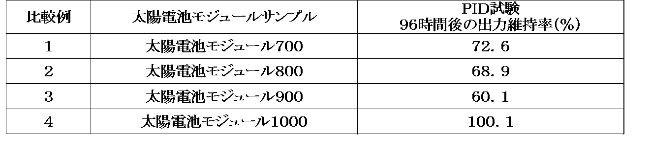
表1に示すように、太陽電池モジュール100、200、300、400、500、600は、試験後の出力維持率(初期)が、100±0.2%以内であり、PID現象が抑制されていることがわかった。
表2に示すように、太陽電池モジュール700、800は、試験後の出力維持率(初期)が、それそれ、72.6%、68.9%であり、PID現象が発生していることがわかった。この結果は、受光面側白板ガラスと太陽電池セルとの間に、シリコーンが存在しないとPIDを抑制できないことを示している。また、太陽電池モジュール900は、試験後の出力維持率(初期)が60.1%であり、PID現象の発生状況が最も大きかった。
太陽電池モジュール1000は、試験後の出力維持率が100.1%であり、PID現象が抑制された。この構造体では、太陽電池モジュールのPID耐性が最も大きいと考えられるが、太陽電池生産コストの問題がある。
表2に示すように、太陽電池モジュール700、800は、試験後の出力維持率(初期)が、それそれ、72.6%、68.9%であり、PID現象が発生していることがわかった。この結果は、受光面側白板ガラスと太陽電池セルとの間に、シリコーンが存在しないとPIDを抑制できないことを示している。また、太陽電池モジュール900は、試験後の出力維持率(初期)が60.1%であり、PID現象の発生状況が最も大きかった。
太陽電池モジュール1000は、試験後の出力維持率が100.1%であり、PID現象が抑制された。この構造体では、太陽電池モジュールのPID耐性が最も大きいと考えられるが、太陽電池生産コストの問題がある。
また、太陽電池モジュール100において、シリコーンの厚みを変更させた評価結果を表3に示す。
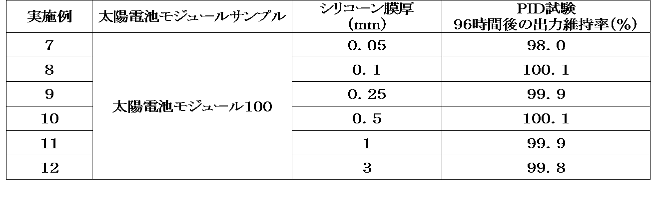
表3に示すように、0.05mmで出力維持率が98.0%であり、シリコーンの厚み0.1、0.25、0.5、1、3mmでは、100±0.2%であった。0.05mm厚でもPID現象抑制効果は得られるが、0.1mm厚以上が望ましい。
以上のように、本発明に関わる太陽電池モジュールは、封止材としてEVAとシリコーンの複合体を用い、かつガラス等からなる透過性基板と太陽電池セルとの間に、該封止複合体を積層することによって、PID発生を抑制でき、かつ太陽電池モジュールの生産コストを大幅に上昇させることなく、容易に良好なラミネート封止を得ることができる。
100、200、300、400、500、600、700、800、900、1000:太陽電池モジュール
101:光透過性基板
102:封止材EVA
103:封止材シリコーン
104:太陽電池素子ストリングス
105:裏面保護材
101:光透過性基板
102:封止材EVA
103:封止材シリコーン
104:太陽電池素子ストリングス
105:裏面保護材
Claims (12)
- 受光面側に光透過性基板を有し、裏面側に裏面保護材を有する太陽電池モジュールであって、受光面側光透過性基板と太陽電池素子との間の封止材として、EVA(エチレン酢酸ビニル共重合体)とシリコーンが隣接かつ積層されている構造であり、太陽電池素子と裏面保護材との間がEVAで封止されている構造であることを特徴とする太陽電池モジュール。
- 受光面側に光透過性基板を有し、裏面側に裏面保護材を有する太陽電池モジュールであって、受光面側光透過性基板と太陽電池素子との間の封止材として、EVA(エチレン酢酸ビニル共重合体)とシリコーンが隣接かつ積層されている構造であり、かつ、裏面保護材と太陽電池素子との間に、EVA(エチレン酢酸ビニル共重合体)とシリコーンが隣接積層されている構造であることを特徴とする太陽電池モジュール。
- 受光面側光透過性基板にEVAが接し、隣接するシリコーンが太陽電池素子に接する構造であることを特徴とする請求項1記載の太陽電池モジュール。
- 受光面側光透過性基板にシリコーンが接し、隣接するEVAが太陽電池素子に接する構造であることを特徴とする請求項1記載の太陽電池モジュール。
- 受光面側光透過性基板及び裏面保護材にEVAがそれぞれ接し、隣接するシリコーンが太陽電池素子にそれぞれ接する構造であることを特徴とする請求項2記載の太陽電池モジュール。
- 受光面側光透過性基板及び裏面保護材にシリコーンがそれぞれ接し、隣接するEVAが太陽電池素子にそれぞれ接する構造であることを特徴とする請求項2記載の太陽電池モジュール。
- 受光面側光透過性基板にEVAが接し、これに隣接するシリコーンが太陽電池素子受光面に接し、かつ裏面保護材にシリコーンが接し、これに隣接するEVAが太陽電池素子裏面に接する構造であることを特徴とする請求項2記載の太陽電池モジュール。
- 受光面側光透過性基板にシリコーンが接し、これに隣接するEVAが太陽電池素子受光面に接し、かつ裏面保護材にEVAが接し、これに隣接するシリコーンが太陽電池素子裏面に接する構造であることを特徴とする請求項2記載の太陽電池モジュール。
- 前記EVAとシリコーンは、EVAとシリコーンが2層構造に重なった複合積層体を形成しており、シリコーンの厚みが0.05~3mmであり、複合積層体の厚みが0.45~3.6mmであることを特徴とする請求項1~8のいずれか1項に記載の太陽電池モジュール。
- 前記シリコーンは、
(A)下記平均組成式(I)
R1 aSiO(4-a)/2 (I)
(式中、R1は同一又は異種の非置換又は置換の1価炭化水素基を示し、aは1.95~2.05の正数である。)
で表される重合度が100以上のオルガノポリシロキサン 100質量部、
(B)比表面積が50m2/g以上の補強性シリカ 20~150質量部、
(C)硬化剤 (A)成分を硬化させる有効量
を含むシリコーン組成物の硬化物であることを特徴とする請求項1~9のいずれか1項に記載の太陽電池モジュール。 - 裏面保護材として裏面光透過性基板が用いられている構造であることを特徴とする請求項1~10のいずれか1項に記載の太陽電池モジュール。
- 前記太陽電池モジュールは、受光面側に光透過性基板を有し、EVAと未加硫状態のシリコーン組成物が2層構造に重なった積層体を光透過性基板に載置させ、その積層体上部に太陽電池素子ストリングスを載置し、太陽電池素子ストリングス背面上に、EVA単層、もしくはEVAと未加硫状態のシリコーン組成物が2層構造に重なった積層体を載置し、最背面側に裏面保護材を積層した後、真空ラミネーターを用いて真空下加熱押圧を行い、未加硫状態のシリコーン組成物及びEVAを架橋させることによりモジュール化することを特徴とする請求項1~11のいずれか1項に記載の太陽電池モジュールの製造方法。
Priority Applications (2)
| Application Number | Priority Date | Filing Date | Title |
|---|---|---|---|
| KR1020177017396A KR20170107977A (ko) | 2015-01-27 | 2015-11-10 | 태양전지 모듈 및 태양전지 모듈의 제조 방법 |
| CN201580074723.9A CN107231819A (zh) | 2015-01-27 | 2015-11-10 | 太阳能电池组件和太阳能电池组件的制造方法 |
Applications Claiming Priority (2)
| Application Number | Priority Date | Filing Date | Title |
|---|---|---|---|
| JP2015-013157 | 2015-01-27 | ||
| JP2015013157A JP6319118B2 (ja) | 2015-01-27 | 2015-01-27 | 太陽電池モジュール及び太陽電池モジュールの製造方法 |
Publications (1)
| Publication Number | Publication Date |
|---|---|
| WO2016121188A1 true WO2016121188A1 (ja) | 2016-08-04 |
Family
ID=56542826
Family Applications (1)
| Application Number | Title | Priority Date | Filing Date |
|---|---|---|---|
| PCT/JP2015/081545 Ceased WO2016121188A1 (ja) | 2015-01-27 | 2015-11-10 | 太陽電池モジュール及び太陽電池モジュールの製造方法 |
Country Status (5)
| Country | Link |
|---|---|
| JP (1) | JP6319118B2 (ja) |
| KR (1) | KR20170107977A (ja) |
| CN (1) | CN107231819A (ja) |
| TW (1) | TWI677107B (ja) |
| WO (1) | WO2016121188A1 (ja) |
Families Citing this family (1)
| Publication number | Priority date | Publication date | Assignee | Title |
|---|---|---|---|---|
| CN111732902B (zh) * | 2020-07-02 | 2024-07-02 | 常州斯威克光伏新材料有限公司 | 一种双面电池用抗极化封装胶膜及其制备方法 |
Citations (8)
| Publication number | Priority date | Publication date | Assignee | Title |
|---|---|---|---|---|
| JPH10321888A (ja) * | 1997-05-21 | 1998-12-04 | Shibata Ind Co Ltd | 太陽電池モジュール用保護シート |
| JPH11103085A (ja) * | 1997-09-29 | 1999-04-13 | Shin Etsu Polymer Co Ltd | 太陽電池とその製造方法及び太陽電池ユニット |
| JP2008235603A (ja) * | 2007-03-20 | 2008-10-02 | Sanyo Electric Co Ltd | 太陽電池モジュール |
| JP2013521640A (ja) * | 2010-03-05 | 2013-06-10 | モメンティブ パフォーマンス マテリアルズ ゲーエムベーハー | 太陽電池モジュールのための封止材としての使用のための硬化性ポリオルガノシロキサン組成物 |
| JP2013153085A (ja) * | 2012-01-25 | 2013-08-08 | Shin Etsu Chem Co Ltd | 太陽電池モジュールの製造方法及び太陽電池モジュール |
| JP2013191673A (ja) * | 2012-03-13 | 2013-09-26 | Fuji Electric Co Ltd | フレキシブル太陽電池モジュール |
| JP2014165296A (ja) * | 2013-02-25 | 2014-09-08 | Panasonic Corp | 太陽電池モジュールおよびその製造方法 |
| JP2014225550A (ja) * | 2013-05-16 | 2014-12-04 | 富士電機株式会社 | 太陽電池モジュール及び太陽電池モジュールの製造方法 |
Family Cites Families (2)
| Publication number | Priority date | Publication date | Assignee | Title |
|---|---|---|---|---|
| JPH10321886A (ja) * | 1997-05-21 | 1998-12-04 | Shibata Ind Co Ltd | 太陽電池モジュールの製造方法 |
| JP5990164B2 (ja) * | 2010-07-02 | 2016-09-07 | スリーエム イノベイティブ プロパティズ カンパニー | 封入材及び光起電セルを有するバリア組立品 |
-
2015
- 2015-01-27 JP JP2015013157A patent/JP6319118B2/ja active Active
- 2015-11-10 WO PCT/JP2015/081545 patent/WO2016121188A1/ja not_active Ceased
- 2015-11-10 CN CN201580074723.9A patent/CN107231819A/zh not_active Withdrawn
- 2015-11-10 KR KR1020177017396A patent/KR20170107977A/ko not_active Withdrawn
- 2015-12-03 TW TW104140553A patent/TWI677107B/zh active
Patent Citations (8)
| Publication number | Priority date | Publication date | Assignee | Title |
|---|---|---|---|---|
| JPH10321888A (ja) * | 1997-05-21 | 1998-12-04 | Shibata Ind Co Ltd | 太陽電池モジュール用保護シート |
| JPH11103085A (ja) * | 1997-09-29 | 1999-04-13 | Shin Etsu Polymer Co Ltd | 太陽電池とその製造方法及び太陽電池ユニット |
| JP2008235603A (ja) * | 2007-03-20 | 2008-10-02 | Sanyo Electric Co Ltd | 太陽電池モジュール |
| JP2013521640A (ja) * | 2010-03-05 | 2013-06-10 | モメンティブ パフォーマンス マテリアルズ ゲーエムベーハー | 太陽電池モジュールのための封止材としての使用のための硬化性ポリオルガノシロキサン組成物 |
| JP2013153085A (ja) * | 2012-01-25 | 2013-08-08 | Shin Etsu Chem Co Ltd | 太陽電池モジュールの製造方法及び太陽電池モジュール |
| JP2013191673A (ja) * | 2012-03-13 | 2013-09-26 | Fuji Electric Co Ltd | フレキシブル太陽電池モジュール |
| JP2014165296A (ja) * | 2013-02-25 | 2014-09-08 | Panasonic Corp | 太陽電池モジュールおよびその製造方法 |
| JP2014225550A (ja) * | 2013-05-16 | 2014-12-04 | 富士電機株式会社 | 太陽電池モジュール及び太陽電池モジュールの製造方法 |
Also Published As
| Publication number | Publication date |
|---|---|
| JP6319118B2 (ja) | 2018-05-09 |
| CN107231819A (zh) | 2017-10-03 |
| KR20170107977A (ko) | 2017-09-26 |
| TWI677107B (zh) | 2019-11-11 |
| JP2016139683A (ja) | 2016-08-04 |
| TW201631789A (zh) | 2016-09-01 |
Similar Documents
| Publication | Publication Date | Title |
|---|---|---|
| JP6217328B2 (ja) | 太陽電池封止用紫外線遮蔽性シリコーン接着剤シート並びにそれを用いた太陽電池モジュール | |
| KR101644809B1 (ko) | 태양전지용 실리콘 봉지재 조성물 및 태양전지 모듈 | |
| CN103636005B (zh) | 太阳能电池组件及其制造方法 | |
| CN104417008A (zh) | 太阳能电池模组的制造 | |
| KR20240136958A (ko) | 태양전지모듈 및 그의 제조방법, 그리고 태양전지봉지재 | |
| JP6784186B2 (ja) | 太陽電池モジュールの製造方法 | |
| JP6269527B2 (ja) | 太陽電池モジュールの製造方法 | |
| JP6319118B2 (ja) | 太陽電池モジュール及び太陽電池モジュールの製造方法 | |
| KR102165215B1 (ko) | 태양 전지 밀봉용 실리콘 접착제 시트 및 그를 이용한 태양 전지 모듈의 제조 방법 | |
| JP2017163064A (ja) | 太陽電池モジュール及び太陽電池モジュールの製造方法 | |
| JP2017191813A (ja) | 太陽電池モジュール及びその製造方法 | |
| JP2019110327A (ja) | 太陽電池モジュール及び太陽電池モジュールの製造方法 | |
| JP2018082073A (ja) | 太陽電池モジュールの製造方法 | |
| JP6512113B2 (ja) | 太陽電池モジュールの製造方法 | |
| WO2019082927A1 (ja) | 太陽電池モジュール | |
| WO2017217133A1 (ja) | 薄膜太陽電池モジュール及びその製造方法 | |
| JP2017163062A (ja) | 太陽電池モジュール及び太陽電池モジュールの製造方法 | |
| JP2017163061A (ja) | 太陽電池モジュール及び太陽電池モジュールの製造方法 |
Legal Events
| Date | Code | Title | Description |
|---|---|---|---|
| 121 | Ep: the epo has been informed by wipo that ep was designated in this application |
Ref document number: 15880080 Country of ref document: EP Kind code of ref document: A1 |
|
| ENP | Entry into the national phase |
Ref document number: 20177017396 Country of ref document: KR Kind code of ref document: A |
|
| NENP | Non-entry into the national phase |
Ref country code: DE |
|
| 122 | Ep: pct application non-entry in european phase |
Ref document number: 15880080 Country of ref document: EP Kind code of ref document: A1 |