WO2016103987A1 - 単結晶の製造方法 - Google Patents
単結晶の製造方法 Download PDFInfo
- Publication number
- WO2016103987A1 WO2016103987A1 PCT/JP2015/082319 JP2015082319W WO2016103987A1 WO 2016103987 A1 WO2016103987 A1 WO 2016103987A1 JP 2015082319 W JP2015082319 W JP 2015082319W WO 2016103987 A1 WO2016103987 A1 WO 2016103987A1
- Authority
- WO
- WIPO (PCT)
- Prior art keywords
- single crystal
- dopant
- added
- crucible
- melt
- Prior art date
- Legal status (The legal status is an assumption and is not a legal conclusion. Google has not performed a legal analysis and makes no representation as to the accuracy of the status listed.)
- Ceased
Links
Images


Classifications
-
- C—CHEMISTRY; METALLURGY
- C30—CRYSTAL GROWTH
- C30B—SINGLE-CRYSTAL GROWTH; UNIDIRECTIONAL SOLIDIFICATION OF EUTECTIC MATERIAL OR UNIDIRECTIONAL DEMIXING OF EUTECTOID MATERIAL; REFINING BY ZONE-MELTING OF MATERIAL; PRODUCTION OF A HOMOGENEOUS POLYCRYSTALLINE MATERIAL WITH DEFINED STRUCTURE; SINGLE CRYSTALS OR HOMOGENEOUS POLYCRYSTALLINE MATERIAL WITH DEFINED STRUCTURE; AFTER-TREATMENT OF SINGLE CRYSTALS OR A HOMOGENEOUS POLYCRYSTALLINE MATERIAL WITH DEFINED STRUCTURE; APPARATUS THEREFOR
- C30B15/00—Single-crystal growth by pulling from a melt, e.g. Czochralski method
- C30B15/02—Single-crystal growth by pulling from a melt, e.g. Czochralski method adding crystallising materials or reactants forming it in situ to the melt
- C30B15/04—Single-crystal growth by pulling from a melt, e.g. Czochralski method adding crystallising materials or reactants forming it in situ to the melt adding doping materials, e.g. for n-p-junction
-
- C—CHEMISTRY; METALLURGY
- C30—CRYSTAL GROWTH
- C30B—SINGLE-CRYSTAL GROWTH; UNIDIRECTIONAL SOLIDIFICATION OF EUTECTIC MATERIAL OR UNIDIRECTIONAL DEMIXING OF EUTECTOID MATERIAL; REFINING BY ZONE-MELTING OF MATERIAL; PRODUCTION OF A HOMOGENEOUS POLYCRYSTALLINE MATERIAL WITH DEFINED STRUCTURE; SINGLE CRYSTALS OR HOMOGENEOUS POLYCRYSTALLINE MATERIAL WITH DEFINED STRUCTURE; AFTER-TREATMENT OF SINGLE CRYSTALS OR A HOMOGENEOUS POLYCRYSTALLINE MATERIAL WITH DEFINED STRUCTURE; APPARATUS THEREFOR
- C30B15/00—Single-crystal growth by pulling from a melt, e.g. Czochralski method
- C30B15/20—Controlling or regulating
-
- C—CHEMISTRY; METALLURGY
- C30—CRYSTAL GROWTH
- C30B—SINGLE-CRYSTAL GROWTH; UNIDIRECTIONAL SOLIDIFICATION OF EUTECTIC MATERIAL OR UNIDIRECTIONAL DEMIXING OF EUTECTOID MATERIAL; REFINING BY ZONE-MELTING OF MATERIAL; PRODUCTION OF A HOMOGENEOUS POLYCRYSTALLINE MATERIAL WITH DEFINED STRUCTURE; SINGLE CRYSTALS OR HOMOGENEOUS POLYCRYSTALLINE MATERIAL WITH DEFINED STRUCTURE; AFTER-TREATMENT OF SINGLE CRYSTALS OR A HOMOGENEOUS POLYCRYSTALLINE MATERIAL WITH DEFINED STRUCTURE; APPARATUS THEREFOR
- C30B29/00—Single crystals or homogeneous polycrystalline material with defined structure characterised by the material or by their shape
- C30B29/02—Elements
- C30B29/06—Silicon
Definitions
- the present invention relates to a method for producing a single crystal.
- an epitaxial silicon wafer for power MOS transistors is required to have a very low substrate resistivity.
- the resistivity to the molten silicon is increased during the pulling process of the single crystal ingot (hereinafter referred to as single crystal), which is the material of the silicon wafer (that is, during the growth of the silicon crystal).
- single crystal which is the material of the silicon wafer (that is, during the growth of the silicon crystal).
- a technique of doping arsenic (As) or antimony (Sb) as an n-type dopant for adjustment is known (see, for example, Patent Document 1).
- This Patent Document 1 discloses that the occurrence of dislocation can be suppressed by producing a single crystal so that the crystal conical part, that is, the shoulder part has an opening angle of 40 ° to 60 °.
- An object of the present invention is to provide a method for producing a single crystal having a low resistivity and suppressed occurrence of dislocation.
- the upper end of the straight body portion is located at the boundary with the shoulder portion, and is, for example, a portion indicated by reference numeral 63A in FIG.
- the dopant concentration of the dopant-added melt was adjusted by adding red phosphorus as a dopant to the silicon melt so that the resistivity at the upper end of the straight body of the single crystal was 1.0 m ⁇ ⁇ cm or less.
- the production conditions were the conditions for producing a single crystal having a diameter of 200 mm and a length of the straight body portion of 860 mm. Moreover, the production was stopped when the single crystal during production was observed and the formation of dislocation was confirmed, and the subsequent steps were not performed. Furthermore, the presence or absence of abnormal growth was also confirmed.
- H is the distance from the lowest part inside the crucible to the melt surface
- R is the radius of the melt surface.
- the melt surface is located in the crucible cylindrical portion (portion where the inner diameter is substantially uniform), and R is 10.72 inches which is half the inner diameter of the crucible. It was.
- the change in resistivity over time is taken into account by taking into account the so-called sampling and pulling method in which a plurality of single crystals are pulled up one by one without adding dopants or silicon melts. Is preferably small.
- the resistivity of the straight body of the single crystal that has been manufactured when the time is 10 hours does not greatly exceed 1.0 m ⁇ ⁇ cm. From this, at least when H / R exceeds 0.4, the resistance of the entire straight body part does not greatly exceed 1.0 m ⁇ ⁇ cm even if the single crystal production is started 10 hours after the addition of the dopant. Can be rate.
- the present invention has been completed based on the above findings.
- the method for producing a single crystal of the present invention is a production of a single crystal by the Czochralski method, and can accommodate a chamber and a dopant-added melt that is arranged in the chamber and added with a dopant to a silicon melt.
- a method for producing a single crystal using a single crystal pulling apparatus comprising a crucible and a pulling portion for pulling a seed crystal after contacting the dopant-added melt, wherein the shoulder forming the shoulder portion of the single crystal Part forming step and a straight body forming step for forming a straight body portion of the single crystal, and the shoulder portion forming step determines a distance from the lowest part inside the crucible to the surface of the dopant-added melt.
- H (mm) the radius of the surface of the dopant-added melt is R (mm)
- the formation of the shoulder is started in a state satisfying the following formula (1). 0.4 ⁇ H / R ⁇ 0.78 (1)
- the dopant is red phosphorus
- the dopant-added melt has the red phosphorus so that the resistivity at the upper end of the straight body portion is 1.0 m ⁇ ⁇ cm or less. Is preferably added.
- the dopant is arsenic, and the arsenic is added to the dopant-added melt so that the resistivity of the upper end of the straight body portion is 2.0 m ⁇ ⁇ cm or less.
- the dopant is antimony
- the dopant-added melt is added with the antimony so that the resistivity at the upper end of the straight body portion is 15 m ⁇ ⁇ cm or less.
- the resistivity at the upper end of the straight body portion is 15 m ⁇ ⁇ cm or less.
- it is. According to the present invention described above, it is possible to obtain a silicon wafer having a desired low resistivity and to produce a single crystal in which the occurrence of dislocations is suppressed.
- the dopant is red phosphorus and germanium
- the dopant-added melt has a resistivity of 1.2 m ⁇ ⁇ cm or less so that a resistivity at an upper end of the straight body portion is 1.2 m ⁇ ⁇ cm or less.
- Red phosphorus and germanium are preferably added. According to the present invention, misfit transition of an epitaxial silicon wafer manufactured using a single crystal can be suppressed.
- an amount of the dopant-added melt capable of producing one single crystal is accommodated in the crucible, and each time the single crystal is produced, a silicon raw material is added to the crucible. It is preferable to produce the next single crystal by adding the dopant.
- the concentration of the dopant in the dopant-added melt at the time of manufacturing each single crystal can be made constant, and the single crystal can be manufactured without performing control in consideration of evaporation of the dopant. .
- an amount of the dopant-added melt capable of producing a plurality of the single crystals is accommodated in the crucible, and the plurality of the plurality of the plurality of single crystals can be produced without adding a silicon raw material and the dopant to the crucible
- One single crystal is preferably produced one by one. According to the present invention, a plurality of single crystals can be manufactured without solidifying (cooling) the dopant-added melt, and the efficiency of single crystal manufacturing can be improved.
- the single crystal pulling apparatus 1 includes a single crystal pulling apparatus main body 3, a doping apparatus (not shown), and a control unit (not shown).
- the single crystal pulling apparatus main body 3 includes a chamber 30, a crucible 31 disposed in the chamber 30, a heating unit 32 that radiates and heats the crucible 31, a pulling cable 33 as a pulling unit, and heat insulation.
- a tube 34 and a shield 36 are provided.
- an inert gas for example, argon gas
- argon gas is introduced at a predetermined gas flow rate from the upper side to the lower side through the introduction unit 30 ⁇ / b> A provided at the upper part under the control of the control unit.
- the pressure in the chamber 30 can be controlled by the control unit.
- the crucible 31 melts polycrystalline silicon, which is a raw material for a silicon wafer, to form a silicon melt 4.
- the crucible 31 includes a bottomed quartz quartz crucible 311 and a graphite graphite crucible 312 which is disposed outside the quartz crucible 311 and accommodates the quartz crucible 311.
- the crucible 31 is supported by a support shaft 37 that rotates at a predetermined speed.
- the outer diameter of the cylindrical portion is 22 inches and the inner diameter is 21.44 inches.
- the heating unit 32 is disposed outside the crucible 31 and heats the crucible 31 to melt the silicon in the crucible 31.
- the pulling cable 33 is connected to, for example, a pulling drive unit (not shown) disposed on the crucible 31. Further, the pulling cable 33 is appropriately attached to the other end with a seed holder 38 for holding a seed crystal or a doping device (not shown).
- the pulling cable 33 is configured to be rotatable by driving a pulling drive unit.
- the pull-up cable 33 is raised at a predetermined pull-up speed under the control of the pull-up drive unit by the control unit.
- the heat insulating cylinder 34 is disposed so as to surround the crucible 31 and the heating unit 32.
- the shield 36 is a heat shielding shield that blocks radiant heat radiated upward from the heating unit 32.
- the doping apparatus is for volatilizing red phosphorus as a solid state dopant and doping the silicon melt 4 in the crucible 31, that is, adding it to generate a dopant added melt 41.
- a doping apparatus a configuration in which the lower end portion of the cylindrical portion is immersed in the silicon melt 4 and red phosphorus is added to the silicon melt 4, or a lower end portion of the cylindrical portion is separated from the silicon melt 4.
- red phosphorus is added to the silicon melt 4 by blowing the volatilized red phosphorus onto the silicon melt 4 can be applied.
- the control unit appropriately controls the gas flow rate in the chamber 30, the pressure in the furnace, and the pulling speed of the pulling cable 33 on the basis of the setting input by the operator, thereby controlling the single crystal 6 during manufacture.
- the single crystal pulling apparatus 1 in which a quartz crucible 311 containing 80 kg of polysilicon material is set as an initial stage heats the polysilicon material under the control of the control unit. After melting, the gas flow rate in the chamber 30 and the furnace pressure are set to a predetermined state, and red phosphorus as a volatile dopant is added to the silicon melt 4 to generate a dopant-added melt 41.
- the amount of red phosphorus added is such that the resistivity of the silicon wafer cut out from the single crystal 6 is 0.6 m ⁇ ⁇ cm to 1.0 m ⁇ ⁇ cm.
- germanium may be added together with red phosphorus. When germanium is added, the amount of red phosphorus and germanium added may be such that the resistivity of the silicon wafer is 1.2 m ⁇ ⁇ cm or less.
- the control unit of the single crystal pulling apparatus 1 immerses the seed crystal in the melt based on the setting input by the operator, and then pulls the seed crystal at a predetermined pulling speed to manufacture the single crystal 6.
- the control unit raises at least the straight body forming step among the neck forming process, the shoulder forming process, the straight body forming process, the tail forming process, and the cooling process in the single crystal 6.
- the single crystal 6 having a shorter dimension than that of the conventional one is manufactured by shortening the time. Specifically, as shown by the solid line in FIG.
- the distance from the lowermost part inside the crucible 31 to the surface 41 ⁇ / b> A of the dopant-added melt 41 is H (mm)
- the radius of the surface 41A being R (mm) and satisfying the above formula (1)
- the formation of the shoulder 62 as shown by the two-dot chain line in FIG. 3 is started.
- the straight body portion 63 and the tail portion 64 are formed as shown by a two-dot chain line in FIG. 3 and FIG.
- the conditions other than the pulling time, for example, the heating conditions by the heating unit 32 may be the same as the conventional one.
- the added melt 41 is accommodated in the crucible 31.
- the single crystal pulling apparatus 1 is used to produce a raw material 411 (silicon, red phosphorus (, Germanium)) is charged into the quartz crucible 311 to satisfy the above formula (1) at the start of the formation of the shoulder 62, and the next single crystal 6 is manufactured.
- the control unit of the single crystal pulling apparatus 1 waits for taking out the single crystal 6 other than the single crystal 6 to be produced lastly and cools it (during the cooling process), the furnace pressure is 13.3 kPa ( It is preferable to adjust to 100 torr) or more and 60 kPa (450 torr) or less.
- red phosphorus which is a volatile dopant, evaporates, and the resistivity of the single crystal 6 to be manufactured next increases.
- the furnace pressure exceeds 60 kPa, the evaporant easily adheres to the inside of the chamber 30 and inhibits single crystallization of the single crystal 6.
- the resistivity of the silicon wafer obtained from the single crystal 6 thus manufactured is 0.6 m ⁇ ⁇ cm or more and 1.0 m ⁇ ⁇ cm or less.
- the single crystal pulling apparatus 1 is used and the same quartz crucible 311 is used and a plurality of dopant-added melts 41 are used.
- the single crystal 6 may be manufactured by a so-called extraction pulling method in which a plurality of single crystals 6 are pulled up one by one.
- the control unit of the single crystal pulling apparatus 1 pulls up the first single crystal and then cools while waiting to take out (during the cooling process). It is preferable to adjust the pressure in the furnace to 13.3 kPa or more and 60 kPa or less.
- the reason why it is preferable to adjust the furnace pressure in this way is the same as the reason for the multi-pull-up method of the above embodiment.
- the above-described pull-up method can be applied without adding a raw material when pulling the last single crystal.
- arsenic may be applied in such an amount that the resistivity of the upper end 63 ⁇ / b> A of the straight body portion 63 is 2.0 m ⁇ ⁇ cm or less, or the upper end of the straight body portion 63.
- An amount of antimony in which the resistivity of 63A is 15 m ⁇ ⁇ cm or less may be applied.
- the diameter of the single crystal may be greater than 200 mm or less than 200 mm.
Landscapes
- Chemical & Material Sciences (AREA)
- Engineering & Computer Science (AREA)
- Crystallography & Structural Chemistry (AREA)
- Materials Engineering (AREA)
- Metallurgy (AREA)
- Organic Chemistry (AREA)
- Crystals, And After-Treatments Of Crystals (AREA)
Abstract
Description
この特許文献1には、結晶円錐部、すなわち肩部が40°~60°の開き角を有するように単結晶を製造することで、有転位化の発生を抑制できることが開示されている。
本発明の目的は、抵抗率が低くかつ有転位化の発生が抑制された単結晶の製造方法を提供することにある。
チョクラルスキー法による単結晶の製造において、坩堝に収容されたドーパント添加融液の中では、坩堝最下部に位置する部分と、融液表面との温度差によって、対流が発生していると考えられる。この対流によって、ドーパント添加融液の下側の熱が、上側に運ばれ、融液表面からの熱放出で温度が下げられた後、下側に戻るため、液温に変動が生じていると考えられる。この液温の変動によって、単結晶に異常成長の発生が増加し、有転位化が発生すると推測した。
また、坩堝内部の最下部から融液表面までの距離が長いほど、ドーパント添加融液の上下での温度差が大きくなるため、対流が強くなると考えられる。
そこで、坩堝にチャージするドーパント添加融液の量を最適化することで、対流に起因する液温の変動が抑制され、有転位化の発生を抑制できる可能性があると推測し、以下の実験を行った。
まず、円筒部の外径が22インチ(558.8mm(1インチ=25.4mm))、かつ、内径が21.10インチ(536.0mm)の坩堝を有する単結晶引き上げ装置を準備した。
そして、種子結晶に連続するネック部を形成するネック部形成工程と、肩部を形成する肩部形成工程と、直胴部を形成する直胴部形成工程と、テール部を形成するテール部形成工程と、テール部形成工程終了後、単結晶を冷却する冷却工程とを行うことで、単結晶を製造する実験を行った。ここで、直胴部の上端とは、肩部との境界に位置し、例えば図4に符号63Aで示す部分である。
なお、単結晶の直胴部上端の抵抗率が1.0mΩ・cm以下となるように、ドーパントとしての赤リンをシリコン融液に添加して、ドーパント添加融液のドーパント濃度を調整した。
また、製造条件は、直胴部の長さが860mmの直径200mm単結晶を製造するための条件とした。
また、製造中の単結晶を観察して、有転位化を確認した時点で製造を中止し、それ以降の工程を行わなかった。さらに、異常成長の有無についても確認した。
実験結果に基づく、シリコン融液量と、ドーパント量と、H/Rと、有転位化の発生位置と、異常成長の有無との関係を図1に示す。
なお、Hは、坩堝内部の最下部から融液表面までの距離であり、Rは、融液表面の半径である。本実験1では、全ての実験条件(トライ1~7)において、融液表面が坩堝円筒部(内径が略均一の部分)に位置し、Rは坩堝の内径の半分の10.72インチであった。
ここで、トライ2~6では、直前のトライ(トライ1~5)の結晶を、単結晶引き上げ装置から取り出してから、単結晶を製造した。また、トライ2,4,5,6を行う前に、ドーパント濃度を調整するために、ドーパントを添加した。
なお、トライ7は、有転位化および異常成長が発生しなかったトライ6の再現性確認テストである。
なお、単結晶が軸方向に成長する過程で、坩堝内シリコン融液が減少することによりH/Rの値は連続して小さくなる。従い、図1には、H/Rの値が0.77よりも小さい場合の記載はないが、トライ6およびトライ7の結果は、0.77よりもH/Rの値が小さくても有転位化および異常成長が発生しないことを示しており、今回のトライ6およびトライ7のシリコン融液の残液量から、少なくともH/Rの値が0.1まで有転位化および異常成長が発生しないことが判明した。実際、H/Rの値が0.6、0.4のトライも実験1の後に行ったが、有転位化および異常成長が発生することはなかった。
単結晶の抵抗率を低くするためのドーパントである、砒素やアンチモンあるいは赤リンは、蒸発しやすいことが分かっている。ドーパント添加融液のドーパント濃度が等しく、かつ、融液の表面積が等しければ、坩堝にチャージされた量が異なっていても、単位時間あたりのドーパントの蒸発量は等しくなると考えられる。このため、ドーパント濃度が等しければ、坩堝にチャージされたドーパント添加融液の量が少ないほど、単位時間あたりのドーパントの蒸発に伴うドーパント濃度の低下が大きいと推測できる。
そこで、実験2として、以下のシミュレーションを行った。
シミュレーション結果を図2に示す。
ここで、製造効率の観点から、ドーパントやシリコン融液を追加せずに、複数の単結晶を1本ずつ連続して引き上げるいわゆる抜き取り引き上げ法を考慮に入れると、時間経過に伴う抵抗率の変化が小さいことが好ましい。また、ドーパント添加後に単結晶の製造をすぐに開始できない場合があることや、1本の単結晶の引き上げに約10時間かかること、あるいは、シリコンウェーハに要求される性能を考慮に入れると、経過時間が10時間のときに製造を開始した単結晶の直胴部の抵抗率が1.0mΩ・cmを大きく超えないことが好ましい。
このことから、少なくともH/Rが0.4を超える場合、ドーパント添加から10時間経過後に単結晶製造を開始しても、直胴部全体の抵抗率を1.0mΩ・cmを大きく超えない抵抗率にできる。
本発明は、上述のような知見に基づいて完成されたものである。
0.4<H/R<0.78 … (1)
本発明の単結晶の製造方法において、前記ドーパントは、砒素であり、前記ドーパント添加融液には、前記直胴部の上端の抵抗率が2.0mΩ・cm以下となるように前記砒素が添加されていることが好ましい。
本発明の単結晶の製造方法において、前記ドーパントは、アンチモンであり、前記ドーパント添加融液には、前記直胴部の上端の抵抗率が15mΩ・cm以下となるように前記アンチモンが添加されていることが好ましい。
以上の本発明によれば、所望の低抵抗率のシリコンウェーハを得ることができかつ有転位化の発生が抑制された単結晶を製造することができる。
本発明によれば、単結晶を用いて製造されたエピタキシャルシリコンウェーハのミスフィット転移を抑制することができる。
本発明によれば、各単結晶を製造するときにおけるドーパント添加融液中のドーパントの濃度を一定にすることができ、ドーパントの蒸発を考慮に入れた制御を行うことなく、単結晶を製造できる。
本発明によれば、ドーパント添加融液を固化する(冷却する)ことなく複数本の単結晶を製造することができ、単結晶製造の効率化を図ることができる。
〔単結晶引き上げ装置の構成〕
まず、単結晶引き上げ装置の構成について説明する。
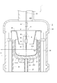
単結晶引き上げ装置1は、図3に示すように、単結晶引き上げ装置本体3と、図示しないドーピング装置と、図示しない制御部とを備える。
単結晶引き上げ装置本体3は、チャンバ30と、このチャンバ30内に配置された坩堝31と、この坩堝31に熱を放射して加熱する加熱部32と、引き上げ部としての引き上げケーブル33と、断熱筒34と、シールド36と備える。
加熱部32は、坩堝31の外側に配置されており、坩堝31を加熱して、坩堝31内のシリコンを融解する。
引き上げケーブル33は、例えば坩堝31上部に配置された図示しない引き上げ駆動部に、一端が接続されている。また、引き上げケーブル33は、他端に、種子結晶を保持するシードホルダ38、または、図示しないドーピング装置が適宜取り付けられる。引き上げケーブル33は、引き上げ駆動部の駆動により回転可能に構成されている。この引き上げケーブル33は、制御部による引き上げ駆動部の制御により、所定の引き上げ速度で上昇する。
断熱筒34は、坩堝31および加熱部32の周囲を取り囲むように配置されている。
シールド36は、加熱部32から上方に向かって放射される輻射熱を遮断する熱遮蔽用シールドである。
制御部は、作業者の設定入力に基づいて、チャンバ30内のガス流量、炉内圧力、引き上げケーブル33の引き上げ速度を適宜制御して、単結晶6製造時の制御をする。
次に、単結晶引き上げ装置1を用いて、単結晶6を製造する方法の一例について説明する。なお、本実施形態では、直胴部の長さが860mmの直径200mmの単結晶を製造する方法について説明する。
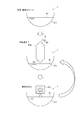
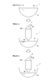
まず、図4を参照して、同一の石英坩堝311を利用し、かつ、単結晶6を引き上げるごとにポリシリコン素材411をチャージして、複数本の単結晶6を引き上げるいわゆるマルチ引き上げ法により、単結晶6を製造する方法について説明する。なお、図3の石英坩堝311の図示を簡略にしている。
ここで、図3および図4に示すように、初期段階として80kgのポリシリコン素材を入れた石英坩堝311がセットされた単結晶引き上げ装置1は、制御部の制御により、ポリシリコン素材を加熱して融解させた後、チャンバ30内のガス流量および炉内圧力を所定の状態にして、シリコン融液4に揮発性ドーパントとしての赤リンを添加してドーパント添加融液41を生成する。
なお、赤リンの添加量は、単結晶6から切り出したシリコンウェーハの抵抗率が、0.6mΩ・cm以上1.0mΩ・cm以下となるような量である。また、エピタキシャルシリコンウェーハのミスフィット転移を抑制するために、赤リンとともにゲルマニウムを添加してもよい。ゲルマニウムを添加する場合、赤リンおよびゲルマニウムの添加量は、シリコンウェーハの抵抗率が、1.2mΩ・cm以下となるような量であってもよい。
この種子結晶の引き上げの際、制御部は、単結晶6におけるネック部形成工程、肩部形成工程、直胴部形成工程、テール部形成工程、冷却工程のうち、少なくとも直胴部形成工程における引き上げ時間を従来よりも短くして、寸法が従来のものより短い単結晶6を製造する。
具体的に、図3中実線で示すように、ネック部61の形成後、坩堝31内部の最下部からドーパント添加融液41の表面41Aまでの距離をH(mm)、ドーパント添加融液41の表面41Aの半径をR(mm)とし、上記式(1)を満たす状態で、図3中二点鎖線で示すような肩部62の形成を開始する。肩部62の形成後、図3中二点鎖線および図4に示すように、直胴部63、テール部64を形成する。
なお、引き上げ時間以外の条件、例えば加熱部32による加熱条件は、従来と同じであってもよい。また、22インチの坩堝31を用いる本実施形態では、肩部62の形成開始時には、37kg(H/R=0.4)を超え、かつ、95kg(H/R=0.78)未満のドーパント添加融液41が坩堝31に収容されている。
以上の工程により、抵抗率が0.6mΩ・cm以上1.0mΩ・cm以下と低く、かつ、有転位化の発生が抑制された単結晶6を製造することができる。
ここで、単結晶引き上げ装置1の制御部は、最後に製造する単結晶6以外の単結晶6の取り出しを待って冷却している間(冷却工程の間)、炉内圧力を13.3kPa(100torr)以上、60kPa(450torr)以下に調整することが好ましい。炉内圧力が13.3kPa未満の場合、揮発性ドーパントである赤リンが蒸発し、次に製造する単結晶6の抵抗率が上昇してしまう。一方、炉内圧力が60kPaを超える場合、蒸発物がチャンバ30内に付着しやすくなり、単結晶6の単結晶化を阻害してしまう。
このように製造された単結晶6から得られるシリコンウェーハの抵抗率は、0.6mΩ・cm以上1.0mΩ・cm以下となる。
なお、本発明は上記実施形態にのみ限定されるものではなく、本発明の要旨を逸脱しない範囲内において種々の改良ならびに設計の変更などが可能である。
ここで、単結晶引き上げ装置1の制御部は、2本の単結晶6を製造する場合、1本目の単結晶を引き上げた後、取り出しを待って冷却している間(冷却工程の間)、炉内圧力を13.3kPa以上、60kPa以下に調整することが好ましい。このように炉内圧力を調整することが好ましい理由は、前記実施形態のマルチ引き上げ法の理由と同じである。
なお、マルチ引上げ法を行う場合でも、最後の単結晶を引上げる際に原料を追加せず、上記抜き取り引上げ法が適用できる。
例えば、初期段階として、肩部62の形成開始時に、H/R=0.68となるようにドーパント添加融液41をチャージして、直胴部の長さが400mmの単結晶6を3回連続で引き上げる方法を適用してもよい。このような方法によっても、抵抗率が0.6mΩ・cm以上1.0mΩ・cm以下と低く、かつ、有転位化の発生が抑制された直径200mmの単結晶を製造することができる。
単結晶の直径は、200mmを超えてもよいし、200mm未満であってもよい。
32インチの坩堝31を用いる場合
118kg(H/R=0.4)を超え、かつ、
300kg(H/R=0.78)未満の量
18インチの坩堝31を用いる場合
19kg(H/R=0.4)を超え、かつ、
52kg(H/R=0.78)未満の量 16インチの坩堝31を用いる場合
14kg(H/R=0.4)を超え、かつ、
36kg(H/R=0.78)未満の量
6…単結晶
30…チャンバ
31…坩堝
33…引き上げ部としての引き上げケーブル
41A…表面
41…ドーパント添加融液
62…肩部
63…直胴部
Claims (7)
- チョクラルスキー法による単結晶の製造であって、
チャンバと、
このチャンバ内に配置されシリコン融液にドーパントを添加したドーパント添加融液を収納可能な坩堝と、
種子結晶を前記ドーパント添加融液に接触させた後に引き上げる引き上げ部と、を備えた単結晶引き上げ装置を利用した単結晶の製造方法であって、
前記単結晶の肩部を形成する肩部形成工程と、
前記単結晶の直胴部を形成する直胴部形成工程とを備え、
前記肩部形成工程は、前記坩堝の内部の最下部から前記ドーパント添加融液の表面までの距離をH(mm)、前記ドーパント添加融液の表面の半径をR(mm)とし、以下の式(1)を満たす状態で、前記肩部の形成を開始することを特徴とする単結晶の製造方法。
0.4<H/R<0.78 … (1) - 請求項1に記載の単結晶の製造方法において、
前記ドーパントは、赤リンであり、
前記ドーパント添加融液には、前記直胴部の上端の抵抗率が1.0mΩ・cm以下となるように前記赤リンが添加されていることを特徴とする単結晶の製造方法。 - 請求項1に記載の単結晶の製造方法において、
前記ドーパントは、砒素であり、
前記ドーパント添加融液には、前記直胴部の上端の抵抗率が2.0mΩ・cm以下となるように前記砒素が添加されていることを特徴とする単結晶の製造方法。 - 請求項1に記載の単結晶の製造方法において、
前記ドーパントは、アンチモンであり、
前記ドーパント添加融液には、前記直胴部の上端の抵抗率が15mΩ・cm以下となるように前記アンチモンが添加されていることを特徴とする単結晶の製造方法。 - 請求項1に記載の単結晶の製造方法において、
前記ドーパントは、赤リンとゲルマニウムであり、
前記ドーパント添加融液には、前記直胴部の上端の抵抗率が1.2mΩ・cm以下となるように前記赤リンと前記ゲルマニウムとが添加されていることを特徴とする単結晶の製造方法。 - 請求項1から請求項5のいずれか一項に記載の単結晶の製造方法において、
1本の前記単結晶を製造可能な量の前記ドーパント添加融液を前記坩堝に収容し、1本の前記単結晶を製造する毎に前記坩堝にシリコン原料および前記ドーパントを追加して、次の前記単結晶を製造することを特徴とする単結晶の製造方法。 - 請求項1から請求項5のいずれか一項に記載の単結晶の製造方法において、
複数本の前記単結晶を製造可能な量の前記ドーパント添加融液を前記坩堝に収容し、前記坩堝にシリコン原料および前記ドーパントを追加することなく、前記複数本の単結晶を1本ずつ製造することを特徴とする単結晶の製造方法。
Priority Applications (4)
| Application Number | Priority Date | Filing Date | Title |
|---|---|---|---|
| DE112015005768.4T DE112015005768B4 (de) | 2014-12-24 | 2015-11-17 | Verfahren zur Herstellung von Monokristall |
| CN201580069135.6A CN107109684B (zh) | 2014-12-24 | 2015-11-17 | 单晶的制造方法 |
| KR1020177020702A KR101953788B1 (ko) | 2014-12-24 | 2015-11-17 | 단결정 제조 방법 |
| US15/535,578 US10329686B2 (en) | 2014-12-24 | 2015-11-17 | Method for producing single crystal |
Applications Claiming Priority (2)
| Application Number | Priority Date | Filing Date | Title |
|---|---|---|---|
| JP2014-261122 | 2014-12-24 | ||
| JP2014261122A JP6471492B2 (ja) | 2014-12-24 | 2014-12-24 | 単結晶の製造方法 |
Publications (1)
| Publication Number | Publication Date |
|---|---|
| WO2016103987A1 true WO2016103987A1 (ja) | 2016-06-30 |
Family
ID=56150020
Family Applications (1)
| Application Number | Title | Priority Date | Filing Date |
|---|---|---|---|
| PCT/JP2015/082319 Ceased WO2016103987A1 (ja) | 2014-12-24 | 2015-11-17 | 単結晶の製造方法 |
Country Status (6)
| Country | Link |
|---|---|
| US (1) | US10329686B2 (ja) |
| JP (1) | JP6471492B2 (ja) |
| KR (1) | KR101953788B1 (ja) |
| CN (1) | CN107109684B (ja) |
| DE (1) | DE112015005768B4 (ja) |
| WO (1) | WO2016103987A1 (ja) |
Cited By (4)
| Publication number | Priority date | Publication date | Assignee | Title |
|---|---|---|---|---|
| WO2019042979A1 (de) * | 2017-09-01 | 2019-03-07 | Siltronic Ag | Einkristall aus silizium mit <100>-orientierung, der mit dotierstoff vom n-typ dotiert ist, und verfahren zur herstellung eines solchen einkristalls |
| CN110249080A (zh) * | 2016-12-20 | 2019-09-17 | 胜高股份有限公司 | 单晶硅的制造方法 |
| US20210040642A1 (en) * | 2017-06-29 | 2021-02-11 | Sumco Corporation | Method for producing silicon single crystal |
| US11702760B2 (en) * | 2017-04-25 | 2023-07-18 | Sumco Corporation | N-type silicon single crystal production method, n-type silicon single crystal ingot, silicon wafer, and epitaxial silicon wafer |
Families Citing this family (7)
| Publication number | Priority date | Publication date | Assignee | Title |
|---|---|---|---|---|
| JP6786905B2 (ja) | 2016-06-27 | 2020-11-18 | 株式会社Sumco | シリコン単結晶の製造方法 |
| JP7080017B2 (ja) * | 2017-04-25 | 2022-06-03 | 株式会社Sumco | n型シリコン単結晶のインゴット、シリコンウェーハ、およびエピタキシャルシリコンウェーハ |
| US12018399B2 (en) * | 2019-08-21 | 2024-06-25 | Meishan Boya Advanced Materials Co., Ltd. | Crystals for detecting neutrons, gamma rays, and x rays and preparation methods thereof |
| US12054848B2 (en) | 2019-08-21 | 2024-08-06 | Meishan Boya Advanced Materials Co., Ltd. | Crystals for detecting neutrons, gamma rays, and x rays and preparation methods thereof |
| CN112513347B (zh) * | 2019-08-21 | 2021-12-24 | 眉山博雅新材料股份有限公司 | 同时具备中子和γ/X射线探测的晶体及其制备方法 |
| CN113463182B (zh) * | 2021-07-07 | 2022-08-23 | 西安奕斯伟硅片技术有限公司 | 一种单晶硅棒的拉制方法 |
| CN113668048A (zh) * | 2021-08-20 | 2021-11-19 | 宁夏中欣晶圆半导体科技有限公司 | 低电阻率重掺磷硅单晶生产装置及方法 |
Citations (7)
| Publication number | Priority date | Publication date | Assignee | Title |
|---|---|---|---|---|
| JPH0761893A (ja) * | 1993-08-26 | 1995-03-07 | Nec Corp | 単結晶育成法 |
| JPH09278581A (ja) * | 1996-04-05 | 1997-10-28 | Sumitomo Sitix Corp | 単結晶製造装置および単結晶製造方法 |
| JP2009057232A (ja) * | 2007-08-31 | 2009-03-19 | Covalent Materials Corp | シリコン単結晶育成方法およびその装置 |
| JP2009215117A (ja) * | 2008-03-11 | 2009-09-24 | Sumco Techxiv株式会社 | シリコン単結晶引上装置及びシリコン単結晶の製造方法 |
| JP2010100474A (ja) * | 2008-10-23 | 2010-05-06 | Covalent Materials Corp | シリコン単結晶引上げ水平磁場の最適化方法およびシリコン単結晶の製造方法 |
| WO2014039976A1 (en) * | 2012-09-10 | 2014-03-13 | GT Advanced CZ, LLC | Continuous czochralski method and apparatus |
| WO2014175120A1 (ja) * | 2013-04-24 | 2014-10-30 | Sumco Techxiv株式会社 | 単結晶の製造方法およびシリコンウェーハの製造方法 |
Family Cites Families (8)
| Publication number | Priority date | Publication date | Assignee | Title |
|---|---|---|---|---|
| JPS555081A (en) | 1978-06-28 | 1980-01-14 | Fujitsu Ltd | Motor construction |
| US6302957B1 (en) * | 1999-10-05 | 2001-10-16 | Sumitomo Metal Industries, Ltd. | Quartz crucible reproducing method |
| DE10025870A1 (de) | 2000-05-25 | 2001-12-06 | Wacker Siltronic Halbleitermat | Einkristallstab und Verfahren zur Herstellung desselben |
| US8021483B2 (en) * | 2002-02-20 | 2011-09-20 | Hemlock Semiconductor Corporation | Flowable chips and methods for the preparation and use of same, and apparatus for use in the methods |
| DE112007001701B4 (de) * | 2006-07-20 | 2018-03-15 | Sumco Techxiv Corp. | Verfahren zur Injektion von Dotierstoff, Dotiervorrichtung und Ziehvorrichtung |
| JP5074826B2 (ja) * | 2007-05-31 | 2012-11-14 | Sumco Techxiv株式会社 | ドーパントの注入方法、及びドーピング装置 |
| JP4829176B2 (ja) * | 2007-06-08 | 2011-12-07 | シルトロニック・ジャパン株式会社 | 単結晶の製造方法 |
| US10544517B2 (en) | 2011-05-06 | 2020-01-28 | Gtat Ip Holding Llc. | Growth of a uniformly doped silicon ingot by doping only the initial charge |
-
2014
- 2014-12-24 JP JP2014261122A patent/JP6471492B2/ja active Active
-
2015
- 2015-11-17 WO PCT/JP2015/082319 patent/WO2016103987A1/ja not_active Ceased
- 2015-11-17 KR KR1020177020702A patent/KR101953788B1/ko active Active
- 2015-11-17 CN CN201580069135.6A patent/CN107109684B/zh active Active
- 2015-11-17 DE DE112015005768.4T patent/DE112015005768B4/de active Active
- 2015-11-17 US US15/535,578 patent/US10329686B2/en active Active
Patent Citations (7)
| Publication number | Priority date | Publication date | Assignee | Title |
|---|---|---|---|---|
| JPH0761893A (ja) * | 1993-08-26 | 1995-03-07 | Nec Corp | 単結晶育成法 |
| JPH09278581A (ja) * | 1996-04-05 | 1997-10-28 | Sumitomo Sitix Corp | 単結晶製造装置および単結晶製造方法 |
| JP2009057232A (ja) * | 2007-08-31 | 2009-03-19 | Covalent Materials Corp | シリコン単結晶育成方法およびその装置 |
| JP2009215117A (ja) * | 2008-03-11 | 2009-09-24 | Sumco Techxiv株式会社 | シリコン単結晶引上装置及びシリコン単結晶の製造方法 |
| JP2010100474A (ja) * | 2008-10-23 | 2010-05-06 | Covalent Materials Corp | シリコン単結晶引上げ水平磁場の最適化方法およびシリコン単結晶の製造方法 |
| WO2014039976A1 (en) * | 2012-09-10 | 2014-03-13 | GT Advanced CZ, LLC | Continuous czochralski method and apparatus |
| WO2014175120A1 (ja) * | 2013-04-24 | 2014-10-30 | Sumco Techxiv株式会社 | 単結晶の製造方法およびシリコンウェーハの製造方法 |
Cited By (11)
| Publication number | Priority date | Publication date | Assignee | Title |
|---|---|---|---|---|
| CN110249080A (zh) * | 2016-12-20 | 2019-09-17 | 胜高股份有限公司 | 单晶硅的制造方法 |
| US11242617B2 (en) | 2016-12-20 | 2022-02-08 | Sumco Corporation | Method for producing silicon single crystal |
| US11702760B2 (en) * | 2017-04-25 | 2023-07-18 | Sumco Corporation | N-type silicon single crystal production method, n-type silicon single crystal ingot, silicon wafer, and epitaxial silicon wafer |
| US20230295835A1 (en) * | 2017-04-25 | 2023-09-21 | Sumco Corporation | N-type silicon single crystal production method, n-type silicon single crystal ingot, silicon wafer, and epitaxial silicon wafer |
| US12252803B2 (en) * | 2017-04-25 | 2025-03-18 | Sumco Corporation | N-type silicon single crystal production method, n-type silicon single crystal ingot, silicon wafer, and epitaxial silicon wafer |
| US20210040642A1 (en) * | 2017-06-29 | 2021-02-11 | Sumco Corporation | Method for producing silicon single crystal |
| US11814745B2 (en) * | 2017-06-29 | 2023-11-14 | Sumco Corporation | Method for producing silicon single crystal |
| US12116691B2 (en) | 2017-06-29 | 2024-10-15 | Sumco Corporation | Method for producing silicon single crystal |
| WO2019042979A1 (de) * | 2017-09-01 | 2019-03-07 | Siltronic Ag | Einkristall aus silizium mit <100>-orientierung, der mit dotierstoff vom n-typ dotiert ist, und verfahren zur herstellung eines solchen einkristalls |
| CN111051578A (zh) * | 2017-09-01 | 2020-04-21 | 硅电子股份公司 | 掺杂有n型掺杂剂的晶向为<100>的硅单晶及其制造方法 |
| US11390962B2 (en) | 2017-09-01 | 2022-07-19 | Siltronic Ag | Single crystal of silicon with <100> orientation, which is doped with n-type dopant, and method for producing such a single crystal |
Also Published As
| Publication number | Publication date |
|---|---|
| DE112015005768T5 (de) | 2017-10-05 |
| JP2016121032A (ja) | 2016-07-07 |
| CN107109684A (zh) | 2017-08-29 |
| KR101953788B1 (ko) | 2019-03-04 |
| KR20170106971A (ko) | 2017-09-22 |
| US10329686B2 (en) | 2019-06-25 |
| CN107109684B (zh) | 2019-08-27 |
| US20170327966A1 (en) | 2017-11-16 |
| DE112015005768B4 (de) | 2020-11-12 |
| JP6471492B2 (ja) | 2019-02-20 |
Similar Documents
| Publication | Publication Date | Title |
|---|---|---|
| JP6471492B2 (ja) | 単結晶の製造方法 | |
| JP6222013B2 (ja) | 抵抗率制御方法 | |
| JP5890587B2 (ja) | 単結晶の製造方法およびシリコンウェーハの製造方法 | |
| JP5892232B1 (ja) | 単結晶の製造方法およびシリコンウェーハの製造方法 | |
| JP5176101B2 (ja) | シリコン単結晶の製造方法および装置並びにシリコン単結晶インゴット | |
| KR102413304B1 (ko) | 에피택셜 실리콘 웨이퍼의 제조 방법 | |
| JP2016060667A (ja) | 抵抗率制御方法、追加ドーパント投入装置、並びに、n型シリコン単結晶 | |
| WO2015075864A1 (ja) | シリコン単結晶の製造方法 | |
| WO2018154874A1 (ja) | シリコン単結晶の製造方法、整流部材、および、単結晶引き上げ装置 | |
| JP6579046B2 (ja) | シリコン単結晶の製造方法 | |
| JP2011157239A (ja) | シリコン単結晶の製造方法およびシリコン単結晶のインゴット | |
| JP6756244B2 (ja) | 半導体シリコン単結晶の製造方法 | |
| JP6786905B2 (ja) | シリコン単結晶の製造方法 | |
| US8308864B2 (en) | Single-crystal manufacturing method | |
| JPWO2005075714A1 (ja) | 単結晶半導体の製造装置および製造方法 | |
| JP2010132470A (ja) | Fz法シリコン単結晶の製造方法 | |
| JP5262346B2 (ja) | シリコン単結晶の製造方法 | |
| TW202140869A (zh) | 單晶矽的製造方法 | |
| JP6922870B2 (ja) | シリコン単結晶の製造方法 | |
| JP6369352B2 (ja) | 結晶育成方法 | |
| KR20140019952A (ko) | 단결정 성장 방법 |
Legal Events
| Date | Code | Title | Description |
|---|---|---|---|
| 121 | Ep: the epo has been informed by wipo that ep was designated in this application |
Ref document number: 15872556 Country of ref document: EP Kind code of ref document: A1 |
|
| WWE | Wipo information: entry into national phase |
Ref document number: 15535578 Country of ref document: US |
|
| WWE | Wipo information: entry into national phase |
Ref document number: 112015005768 Country of ref document: DE |
|
| ENP | Entry into the national phase |
Ref document number: 20177020702 Country of ref document: KR Kind code of ref document: A |
|
| 122 | Ep: pct application non-entry in european phase |
Ref document number: 15872556 Country of ref document: EP Kind code of ref document: A1 |