WO2016103608A1 - 多結晶シリコン棒、多結晶シリコン棒の加工方法、多結晶シリコン棒の結晶評価方法、および、fz単結晶シリコンの製造方法 - Google Patents
多結晶シリコン棒、多結晶シリコン棒の加工方法、多結晶シリコン棒の結晶評価方法、および、fz単結晶シリコンの製造方法 Download PDFInfo
- Publication number
- WO2016103608A1 WO2016103608A1 PCT/JP2015/006142 JP2015006142W WO2016103608A1 WO 2016103608 A1 WO2016103608 A1 WO 2016103608A1 JP 2015006142 W JP2015006142 W JP 2015006142W WO 2016103608 A1 WO2016103608 A1 WO 2016103608A1
- Authority
- WO
- WIPO (PCT)
- Prior art keywords
- polycrystalline silicon
- silicon rod
- crystal
- value
- rod
- Prior art date
- Legal status (The legal status is an assumption and is not a legal conclusion. Google has not performed a legal analysis and makes no representation as to the accuracy of the status listed.)
- Ceased
Links
Images


Classifications
-
- C—CHEMISTRY; METALLURGY
- C01—INORGANIC CHEMISTRY
- C01B—NON-METALLIC ELEMENTS; COMPOUNDS THEREOF; METALLOIDS OR COMPOUNDS THEREOF NOT COVERED BY SUBCLASS C01C
- C01B33/00—Silicon; Compounds thereof
- C01B33/02—Silicon
-
- C—CHEMISTRY; METALLURGY
- C01—INORGANIC CHEMISTRY
- C01B—NON-METALLIC ELEMENTS; COMPOUNDS THEREOF; METALLOIDS OR COMPOUNDS THEREOF NOT COVERED BY SUBCLASS C01C
- C01B33/00—Silicon; Compounds thereof
- C01B33/02—Silicon
- C01B33/021—Preparation
- C01B33/027—Preparation by decomposition or reduction of gaseous or vaporised silicon compounds other than silica or silica-containing material
- C01B33/035—Preparation by decomposition or reduction of gaseous or vaporised silicon compounds other than silica or silica-containing material by decomposition or reduction of gaseous or vaporised silicon compounds in the presence of heated filaments of silicon, carbon or a refractory metal, e.g. tantalum or tungsten, or in the presence of heated silicon rods on which the formed silicon is deposited, a silicon rod being obtained, e.g. Siemens process
-
- C—CHEMISTRY; METALLURGY
- C30—CRYSTAL GROWTH
- C30B—SINGLE-CRYSTAL GROWTH; UNIDIRECTIONAL SOLIDIFICATION OF EUTECTIC MATERIAL OR UNIDIRECTIONAL DEMIXING OF EUTECTOID MATERIAL; REFINING BY ZONE-MELTING OF MATERIAL; PRODUCTION OF A HOMOGENEOUS POLYCRYSTALLINE MATERIAL WITH DEFINED STRUCTURE; SINGLE CRYSTALS OR HOMOGENEOUS POLYCRYSTALLINE MATERIAL WITH DEFINED STRUCTURE; AFTER-TREATMENT OF SINGLE CRYSTALS OR A HOMOGENEOUS POLYCRYSTALLINE MATERIAL WITH DEFINED STRUCTURE; APPARATUS THEREFOR
- C30B13/00—Single-crystal growth by zone-melting; Refining by zone-melting
- C30B13/28—Controlling or regulating
- C30B13/30—Stabilisation or shape controlling of the molten zone, e.g. by concentrators, by electromagnetic fields; Controlling the section of the crystal
-
- C—CHEMISTRY; METALLURGY
- C30—CRYSTAL GROWTH
- C30B—SINGLE-CRYSTAL GROWTH; UNIDIRECTIONAL SOLIDIFICATION OF EUTECTIC MATERIAL OR UNIDIRECTIONAL DEMIXING OF EUTECTOID MATERIAL; REFINING BY ZONE-MELTING OF MATERIAL; PRODUCTION OF A HOMOGENEOUS POLYCRYSTALLINE MATERIAL WITH DEFINED STRUCTURE; SINGLE CRYSTALS OR HOMOGENEOUS POLYCRYSTALLINE MATERIAL WITH DEFINED STRUCTURE; AFTER-TREATMENT OF SINGLE CRYSTALS OR A HOMOGENEOUS POLYCRYSTALLINE MATERIAL WITH DEFINED STRUCTURE; APPARATUS THEREFOR
- C30B29/00—Single crystals or homogeneous polycrystalline material with defined structure characterised by the material or by their shape
- C30B29/02—Elements
- C30B29/06—Silicon
-
- C—CHEMISTRY; METALLURGY
- C30—CRYSTAL GROWTH
- C30B—SINGLE-CRYSTAL GROWTH; UNIDIRECTIONAL SOLIDIFICATION OF EUTECTIC MATERIAL OR UNIDIRECTIONAL DEMIXING OF EUTECTOID MATERIAL; REFINING BY ZONE-MELTING OF MATERIAL; PRODUCTION OF A HOMOGENEOUS POLYCRYSTALLINE MATERIAL WITH DEFINED STRUCTURE; SINGLE CRYSTALS OR HOMOGENEOUS POLYCRYSTALLINE MATERIAL WITH DEFINED STRUCTURE; AFTER-TREATMENT OF SINGLE CRYSTALS OR A HOMOGENEOUS POLYCRYSTALLINE MATERIAL WITH DEFINED STRUCTURE; APPARATUS THEREFOR
- C30B35/00—Apparatus not otherwise provided for, specially adapted for the growth, production or after-treatment of single crystals or of a homogeneous polycrystalline material with defined structure
- C30B35/007—Apparatus for preparing, pre-treating the source material to be used for crystal growth
-
- G—PHYSICS
- G01—MEASURING; TESTING
- G01N—INVESTIGATING OR ANALYSING MATERIALS BY DETERMINING THEIR CHEMICAL OR PHYSICAL PROPERTIES
- G01N23/00—Investigating or analysing materials by the use of wave or particle radiation, e.g. X-rays or neutrons, not covered by groups G01N3/00 – G01N17/00, G01N21/00 or G01N22/00
- G01N23/20—Investigating or analysing materials by the use of wave or particle radiation, e.g. X-rays or neutrons, not covered by groups G01N3/00 – G01N17/00, G01N21/00 or G01N22/00 by using diffraction of the radiation by the materials, e.g. for investigating crystal structure; by using scattering of the radiation by the materials, e.g. for investigating non-crystalline materials; by using reflection of the radiation by the materials
-
- G—PHYSICS
- G01—MEASURING; TESTING
- G01N—INVESTIGATING OR ANALYSING MATERIALS BY DETERMINING THEIR CHEMICAL OR PHYSICAL PROPERTIES
- G01N23/00—Investigating or analysing materials by the use of wave or particle radiation, e.g. X-rays or neutrons, not covered by groups G01N3/00 – G01N17/00, G01N21/00 or G01N22/00
- G01N23/20—Investigating or analysing materials by the use of wave or particle radiation, e.g. X-rays or neutrons, not covered by groups G01N3/00 – G01N17/00, G01N21/00 or G01N22/00 by using diffraction of the radiation by the materials, e.g. for investigating crystal structure; by using scattering of the radiation by the materials, e.g. for investigating non-crystalline materials; by using reflection of the radiation by the materials
- G01N23/207—Diffractometry using detectors, e.g. using a probe in a central position and one or more displaceable detectors in circumferential positions
-
- C—CHEMISTRY; METALLURGY
- C30—CRYSTAL GROWTH
- C30B—SINGLE-CRYSTAL GROWTH; UNIDIRECTIONAL SOLIDIFICATION OF EUTECTIC MATERIAL OR UNIDIRECTIONAL DEMIXING OF EUTECTOID MATERIAL; REFINING BY ZONE-MELTING OF MATERIAL; PRODUCTION OF A HOMOGENEOUS POLYCRYSTALLINE MATERIAL WITH DEFINED STRUCTURE; SINGLE CRYSTALS OR HOMOGENEOUS POLYCRYSTALLINE MATERIAL WITH DEFINED STRUCTURE; AFTER-TREATMENT OF SINGLE CRYSTALS OR A HOMOGENEOUS POLYCRYSTALLINE MATERIAL WITH DEFINED STRUCTURE; APPARATUS THEREFOR
- C30B13/00—Single-crystal growth by zone-melting; Refining by zone-melting
Definitions
- the present invention relates to a polycrystalline silicon rod manufacturing technique, and more particularly to a polycrystalline silicon rod manufacturing technique suitable as a raw material for producing single crystal silicon by the FZ method.
- Single crystal silicon which is indispensable for manufacturing semiconductor devices and the like is crystal grown by the CZ method or the FZ method, and a polycrystalline silicon block or a polycrystalline silicon rod is used as a raw material at that time.
- Such polycrystalline silicon materials are often manufactured by the Siemens method (see Patent Document 1 (Japanese Patent Publication No. 37-18861) and the like).
- the Siemens method refers to vapor phase growth (deposition) of polycrystalline silicon on the surface of a silicon core wire by bringing a silane source gas such as trichlorosilane or monosilane into contact with the heated silicon core wire by CVD (Chemical Vapor Deposition) method. It is a way to
- a polycrystalline silicon block is charged in a quartz crucible, and a seed crystal is immersed in a silicon melt obtained by heating and melting this to eliminate dislocation lines. After dislocation-free, the diameter is gradually expanded to a predetermined diameter, and crystal pulling is performed at a constant speed. At this time, if unmelted polycrystalline silicon remains in the silicon melt, this unmelted polycrystalline piece floats in the vicinity of the solid-liquid interface by convection, causing the occurrence of dislocations and causing the crystal lines to disappear. It becomes a cause.
- Patent Document 2 Japanese Patent Application Laid-Open No. 2014-0010966 discloses a technique for selecting polycrystalline silicon suitable as a raw material for producing single crystal silicon with high quantitativeness and reproducibility, and contributing to stable production of single crystal silicon. Disclosed is a method of evaluating the degree of crystal orientation of polycrystalline silicon by X-ray diffraction, for the purpose of providing the same.
- the value obtained by dividing the maximum value of the plurality of baseline diffraction intensity values for the Miller index surface ⁇ 111> by the minimum value is 1.5 or less, and the Miller index surface ⁇ 220
- the value obtained by dividing the maximum value of the plurality of baseline diffraction intensity values by> by the minimum value is also 1.9 or less, and the division value (I ⁇ 111> / I ⁇ 220>) for any plate-like sample. It has been reported that a polycrystalline silicon rod having a of less than 2.5 is suitable as a raw material for growing single crystal silicon.
- Patent Document 3 Japanese Patent Application Laid-Open No. 2013-217653 also discloses a technique for selecting polycrystalline silicon suitable as a raw material for producing single crystal silicon with high quantitativeness and reproducibility, and contributing to stable production of single crystal silicon. Disclosed is a method of evaluating the degree of crystal orientation of polycrystalline silicon by X-ray diffraction, for the purpose of providing the same.
- peaks may appear in the ⁇ scan chart, and the smaller the number of such peaks, the half width thereof It is described that the narrower the width is, the more suitable the raw material for producing single crystal silicon, and the number of peaks appearing in the ⁇ scan chart is a disk for any of Miller's index planes ⁇ 111> and ⁇ 220>.
- Patent Document 4 Japanese Patent Laid-Open No. 2014-031297 also discloses a technique for selecting polycrystalline silicon suitable as a raw material for producing single crystal silicon with high quantitativeness and reproducibility, and contributing to stable production of single crystal silicon. Disclosed is a method for selecting polycrystalline silicon rods to be used as a raw material for producing single crystal silicon, for the purpose of providing.
- an electron backscattering diffraction image obtained by irradiating the main surface of a plate-like sample collected from a polycrystalline silicon rod with an electron beam is analyzed, and crystal grains having a grain size of 0.5 ⁇ m or more are not detected.
- the total area of the regions is 10% or less of the total area irradiated with the electron beam (condition 1), and the number of crystal grains having a grain size of 0.5 ⁇ m or more and less than 3 ⁇ m was detected.
- a polycrystalline silicon rod which simultaneously satisfies 45% or more of the whole of the crystal grains (condition 2) is selected as a raw material for producing single crystal silicon.
- Patent Document 5 Japanese Patent Laid-Open No. 2014-034506 also discloses a technique for selecting polycrystalline silicon suitable as a raw material for producing single crystal silicon with high quantitativeness and reproducibility, and contributing to stable production of single crystal silicon. Disclosed is a method for selecting polycrystalline silicon rods to be used as a raw material for producing single crystal silicon, for the purpose of providing.
- a plate-like sample having as a main surface a cross section perpendicular to the radial direction of a polycrystalline silicon rod grown by deposition by a chemical growth method is collected, and the thermal diffusivity ⁇ (T) of this plate-like sample Of the thermal diffusivity ratio ( ⁇ (T) / ⁇ R (T)) compared to the thermal diffusivity ⁇ R (T) of a standard sample, which is suitable as a raw material for single crystal silicon production.
- ⁇ (T) / ⁇ R (T) compared to the thermal diffusivity ⁇ R (T) of a standard sample, which is suitable as a raw material for single crystal silicon production. It is a method of selecting a polycrystalline silicon rod. It has been reported that when single crystal silicon is grown using a polycrystalline silicon rod selected in this manner, the crystal lines do not disappear, and stable manufacture of single crystal silicon becomes possible.
- the distribution state of various properties in the stretching direction is important as in the distribution state of various properties in the growth direction (radial direction).
- the characteristics of the crystal include, for example, the amount of crystal formation, crystal orientation, crystal grain size, crystal grain size, thermal diffusivity, thermal conductivity and the like.
- the “shape uniformity” of polycrystalline silicon rods is also important. This is because when the “shape uniformity” in the stretching direction (axial direction) of the polycrystalline silicon rod is low, heat is not transferred uniformly, so that the crystal habit line showing that it is in the dislocation-free state disappears (with (Dislocation).
- the present invention has been made in view of such circumstances, and the object of the present invention is polycrystalline silicon suitable as a raw material for producing single crystal silicon by the FZ method, which is excellent in shape uniformity and crystal characteristic uniformity. It is about providing technology for obtaining a stick.
- the polycrystalline silicon rod according to the first aspect of the present invention is a polycrystalline silicon rod used as a raw material for producing single crystal silicon by the FZ method, and the polycrystalline silicon rod has a full length Is 500 mm or more, and the difference ⁇ D 1 between the maximum value D max and the minimum value D min of the diameter over the entire length is 3 mm or less.
- the average diameter of the polycrystalline silicon rod is 300 mm or less.
- the polycrystalline silicon rod according to the second aspect of the present invention is a polycrystalline silicon rod used as a raw material for producing single crystal silicon by the FZ method, wherein the polycrystalline silicon rod has a total length of 500 mm or more, the difference [Delta] D 2 of the maximum value D max and the minimum value D min of approximately the diameter of the cylindrical virtual rotary body which is formed when rotated at the center axis of the extending direction of the crystal silicon rod is 6mm or less.
- the average diameter of the polycrystalline silicon rod is 300 mm or less.
- the method of processing a polycrystalline silicon rod according to the first aspect of the present invention is a method of processing a polycrystalline silicon rod used as a raw material for producing single crystal silicon by the FZ method, wherein the polycrystalline silicon rod is manufactured by Siemens method It is a polycrystalline silicon rod grown with a total length of 500 mm or more, and the side surface of the polycrystalline silicon rod such that the difference ⁇ D 1 between the maximum value D max and the minimum value D min of the diameter over the entire length is 3 mm or less. Cylindrical grinding.
- the method for processing a polycrystalline silicon rod according to the second aspect of the present invention is a method for processing a polycrystalline silicon rod used as a raw material for producing single crystal silicon by the FZ method, wherein said polycrystalline silicon rod is manufactured by Siemens method
- the maximum length D max of the diameter of a substantially cylindrical virtual rotary body formed when the grown polycrystalline silicon rod having a total length of 500 mm or more and rotated about the central axis in the extending direction of the polycrystalline silicon rod The side surface of the polycrystalline silicon rod is cylindrically ground so that the difference ⁇ D 2 of the minimum value D min is 6 mm or less.
- the crystal evaluation method for polycrystalline silicon rods according to the present invention is a crystal evaluation method for polycrystalline silicon rods used as a raw material for producing single crystal silicon by FZ method, and the diameter of polycrystalline silicon rods grown by Siemens method
- a plurality of plate-like samples having a cross section perpendicular to the direction as the main surface are taken at equal intervals in the radial direction, the crystal characteristic value of the plate-like sample is determined by measurement, and the relative crystal of the portion from which the plate-like sample is taken
- the uniformity of the rod of polycrystalline silicon is evaluated by the evaluation value obtained by multiplying the crystal characteristic value by the amount.
- the evaluation value is determined for two samples collected from the central axis of the polycrystalline silicon rod and the site at the target position, and the rotational symmetry is calculated by the following equation from the two evaluation values A and B obtained. And the step of evaluating whether the average value in the axial direction of the rotational symmetry is 40% or more. 100- (
- two samples are taken at the same radial distance from the central axis of the polycrystalline silicon rod and are located on the same generatrix when cylindrically approximating the polycrystalline silicon rod.
- the evaluation value is determined, and the rotational symmetry difference is calculated from the obtained two evaluation values C and D by the following equation, and it is determined whether the average value of the rotational symmetry difference in the axial direction is 40% or less There is a step of evaluating. (
- the crystal characteristics are, for example, any of crystal formation amount, crystal orientation, crystal grain size, thermal diffusivity, and thermal conductivity.
- the method for producing FZ single crystal silicon according to the present invention is a method for producing FZ single crystal silicon using a polycrystalline silicon rod as a raw material, wherein the polycrystalline silicon rod bridges one pair (two) of silicon cores.
- a polycrystalline silicon rod collected from the leg portion of the inverted U-shaped polycrystalline silicon portion obtained by forming polycrystalline silicon by forming an inverted U-shaped member by interposing The zone floating melting process is started from the bridge vicinity of the polycrystalline silicon rod, with the end side being the bridge vicinity in the precipitation furnace and the other end being the electrode vicinity in the precipitation furnace It is characterized by
- a new evaluation value of “characteristic value ⁇ relative crystal amount” is introduced, and based on this, one having “rotational symmetry” of 40% or more is suitable as a raw material for producing single crystal silicon by the FZ method. Adopted as a polycrystalline silicon rod. Moreover, the thing whose "rotational-symmetry difference" is 40% or less is employ
- a technique for obtaining a polycrystalline silicon rod suitable as a raw material for producing single crystal silicon by the FZ method which is excellent in shape uniformity and crystal characteristic uniformity.
- a polycrystalline silicon rod suitable as a raw material for producing single crystal silicon by the FZ method has high “shape uniformity” in the extending direction (axial direction) of the polycrystalline silicon rod, and polycrystalline silicon
- the present invention is achieved as a result of a sincere study based on the recognition that it is necessary not only the crystal property uniformity in the growth direction (diameter direction) of the rod but also the crystal property uniformity in the extension direction (axis direction) to be high. It came to Hereinafter, embodiments of the present invention will be described with reference to the drawings.
- the cross section of the polycrystalline silicon rod immediately after obtained by the Siemens method is often slightly elliptical instead of perfect perfect circle.
- the cross-sectional shape in the stretching direction (axial direction) often varies from part to part. That is, the polycrystalline silicon rod as grown by the Siemens method is not “uniform in shape” in the stretching direction (axial direction).
- the “shape uniformity” in the stretching direction (axial direction) of the polycrystalline silicon rod is low, no dislocation occurs when this is used as a raw material for producing single crystal silicon by the FZ method.
- the crystal habit line which shows that it is in the state may disappear (it is made to have dislocation). This is because the conduction of heat does not occur constantly in the continuous state change of melting, convection, and solidification due to high frequency heating.
- the "roundness" of the cross section of the polycrystalline silicon rod is suitable as a raw material for producing single crystal silicon by the FZ method, it is further rotated about the central axis in the extending direction of the polycrystalline silicon rod.
- Polycrystalline silicon rods are evaluated with a total length of 500 mm or more and an average diameter of 300 mm or less (5 to 12 inches in diameter). Judgment of "preferred” is made based on the presence or absence of the loss of crystal habit line.
- the maximum value D max and the minimum value D The condition is that the difference ⁇ D 2 of min is 6 mm or less.
- the difference [Delta] D 2 of the maximum value D max and the minimum value D min is the time of rotating grips the polycrystalline silicon rod in actual FZ process, it corresponds to the variation width in the radial direction.
- the polycrystalline silicon rod according to the present invention is a polycrystalline silicon rod used as a raw material for producing single crystal silicon by the FZ method, wherein the polycrystalline silicon rod has a total length of 500 mm or more and extends over the entire length
- the difference ⁇ D 1 between the maximum value D max and the minimum value D min of the diameter is 3 mm or less.
- the side surface of the polycrystalline silicon rod is formed by cylindrical grinding.
- the method of processing a polycrystalline silicon rod according to the present invention is a method of processing a polycrystalline silicon rod used as a raw material for producing single crystal silicon by the FZ method, and the polycrystalline silicon rod is grown by the Siemens method
- the side of the polycrystalline silicon rod is cylindrically ground such that the difference ⁇ D 1 between the maximum value D max and the minimum value D min of the diameter over the entire length is 3 mm or less.
- the polycrystalline silicon rod according to the present invention is a polycrystalline silicon rod used as a raw material for producing single crystal silicon by the FZ method, and the polycrystalline silicon rod has a total length of 500 mm or more, and the polycrystalline silicon rod
- the difference ⁇ D 2 between the maximum value D max and the minimum value D min of the diameter of the substantially cylindrical virtual rotating body formed when it is rotated about the central axis in the drawing direction is 6 mm or less.
- the side surface of the polycrystalline silicon rod is formed by cylindrical grinding.
- the method of processing a polycrystalline silicon rod according to the present invention is a method of processing a polycrystalline silicon rod used as a raw material for producing single crystal silicon by the FZ method, and the polycrystalline silicon rod is grown by the Siemens method
- the maximum value D max and the minimum value D of the diameter of a substantially cylindrical virtual rotating body which is a polycrystalline silicon rod having a total length of 500 mm or more and which is formed when it is rotated about the central axis in the stretching direction of the polycrystalline silicon rod so that the difference [Delta] D 2 of min is 6mm or less and cylindrical grinding the side surfaces of the polycrystalline silicon rod.
- single crystal growth is performed by melting, zone melting and solidification while holding and rotating a polycrystalline silicon rod, so the growth direction (diameter direction) of the polycrystalline silicon rod It is also necessary to evaluate the rotational symmetry when evaluating the crystal characteristic value (or its distribution) of
- the polycrystalline silicon rod is cylindrical
- the polycrystal amount at the growth distance d from the center is in proportion to the square of d
- the polycrystal amount is smaller toward the center side, and the polycrystal is closer to the outer side
- the quantity will increase.
- the inventors of the present invention have found that the thermal stability during the FZ process, the thermal load, and the convective effect of the melt inside the melt are not mere crystal characteristic values, but the amount of polycrystals contributing to the crystal characteristic values. It considered that it was the evaluation value (characteristic value x amount of crystals) which multiplied by, and came to form this invention.
- the present inventors define a new evaluation value (characteristic value x crystal amount) including the crystal growth amount in the growth direction (diameter direction), and evaluate the uniformity of the crystal characteristics in the growth direction (diameter direction).
- characteristic value x crystal amount including the crystal growth amount in the growth direction (diameter direction), and evaluate the uniformity of the crystal characteristics in the growth direction (diameter direction).
- evaluation value ⁇ relative crystal amount is, for example, as follows.
- FIG. 1 is a view for explaining an example of a method for collecting a sample to be used for characteristic value evaluation, and in the example shown in this figure, the diameter grown by deposition on the silicon core wire 1 by Siemens is about 150 mm
- the rod 11 having a diameter of approximately 20 mm and a length of approximately 750 mm is perpendicular to the axial direction of the polycrystalline silicon rod from the side near the bridge of the polycrystalline silicon rod 10, that is, the side located at the highest position in the furnace.
- the holes are taken out and collected, and a total of 16 plate-like samples 12 with a thickness of approximately 2 mm are collected at 10 mm intervals. Then, for each of these plate-like samples 12, the Bragg reflection intensity from the mirror index planes ⁇ 111> and ⁇ 220> is determined.
- the rod 11 having a diameter of about 20 mm and a length of about 750 mm is The sample is hollowed out in a direction perpendicular to the direction, and a total of 16 plate-like samples 12 with a thickness of approximately 2 mm are collected at 10 mm intervals. Then, for each of these plate-like samples 12, the Bragg reflection intensity from the mirror index planes ⁇ 111> and ⁇ 220> is determined.
- the symmetry in the growth direction (radial direction) of each portion of these polycrystalline silicon rods is evaluated by the product of the diffraction intensity value as a crystal characteristic value and the relative crystal amount.
- the “relative crystal amount” for calculating the evaluation value is first obtained by squaring the distance d from the center of the portion from which each plate-like sample was collected to obtain d 2 . Then, the difference ⁇ d 2 between the d 2 values of the plate-like samples collected in close proximity is determined.
- Table 2 shows the sampling position (d) for a total of 16 plate-like samples (SPL) collected from the vicinity of the electrode (the part located at the lowest position in the furnace), the value d 2 obtained by squaring the d,
- the difference ⁇ d 2 with the d 2 value of the adjacent plate-like sample, the Bragg reflection intensities (I ⁇ 111> and I ⁇ 220> ) from the measured Miller index planes ⁇ 111> and ⁇ 220>, these I ⁇ 111 > and I to ⁇ 220> is a table summarizing the difference [Delta] d 2 a multiplied by the obtained evaluation value (I ⁇ 111> ⁇ [Delta] d 2 and I ⁇ 220> ⁇ [Delta] d 2).
- the average value of “rotational symmetry” is 91% for ⁇ 111> and 84% for ⁇ 220>.
- FIG. 2 is a graph of the evaluation values obtained from the total of 32 plate samples.
- the “rotational symmetry” in Tables 1 and 2 is a value in which the difference between the evaluation values obtained from plate-like samples equidistantly spaced from the central axis is represented by% in the following procedure.
- the plate-like sample 6 since the plate-like sample 6 has a distance d of 2 cm from the center, the plate-like sample that is equidistantly symmetrical with this is the sample 11, and the evaluation value for the Miller index plane ⁇ 111>
- the difference is 3,025.
- This value of 3,025 is divided by the average of 27,275 of the above evaluation values, and the value expressed as% is 11.1%.
- the value obtained by subtracting 11.1% from 100% is 88.9%, and this value is referred to as "rotational symmetry”.
- Table 3 is a table summarizing the "rotational symmetry difference" in the axial direction obtained by the above calculation.
- the average value of the “rotational symmetry difference” is 10% for ⁇ 111> and 17% for ⁇ 220>.
- the criterion that the "rotational symmetry difference" is 40% or less is when the value of FZ, L% is obtained 66% or more from the relationship between actual FZ, L% and the actual value of the evaluation value calculated from the characteristic value. It is because it was 40% when it asked for the value of the difference in the evaluation value of. In addition, it was judged that the number of n at the time of this judgment is sufficient, and a highly significant correlation is recognized with respect to the judgment standard calculated from the risk rate of 1%, which is statistically calculated.
- FZ, L% refers to the crystal line provided in crystalline silicon obtained by crystal growth in one FZ operation when the length of the rod of polycrystalline silicon is 100.
- the length of the polycrystalline silicon rod existing in a perfect state is represented by%.
- incomplete crystallographic line there are not only the disappearance of crystallographic line but also disorder or bending of crystallographic line.
- FZ and L% are all values obtained in one FZ operation, not values obtained in a plurality of FZ operations. This is because performing two or more FZ operations leads to a decrease in productivity, and is not targeted by the present invention.
- FZ and L% do not necessarily have to be 100%, but higher values are preferable, and the lower limit thereof is about 60 to 70% in consideration of productivity, and the lower limit is practically used. I can not do it.
- crystal properties are, for example, physical property values such as crystal formation amount, crystal orientation, crystal grain size, thermal diffusivity, thermal conductivity, etc.
- the distribution of those characteristic values may be adopted as the crystal characteristic.
- “Rotational symmetry” generally tends to be lower near the electrodes than near the bridge. This tendency is the same even if the conditions at the time of polycrystalline silicon deposition are changed.
- the lower crystal temperature in the furnace is closer to the carbon electrode being cooled during the reaction process, so the CVD temperature is lower than the higher crystal sites in the furnace Is considered.
- the middle region will be within the range of these two evaluation values, so it is not necessary to evaluate the other regions. That is, evaluation of two points in the height direction determines the evaluation value of the polycrystalline silicon rod as a whole, and at the same time, an approximate profile in the rod is grasped.
- the present invention unlike the simple physical property measuring method in the growth direction (radial direction) as disclosed in Patent Documents 2 to 5, introduces a new evaluation value in consideration of the crystal amount in the radial direction, and further, It is an evaluation method that also considers the (rotational) symmetry of the crystal in the axial direction.
- the uniformity of the crystal near the carbon electrode is generally lower than that near the bridge, when starting zone melting in the single crystal silicon manufacturing process by the FZ method, the one starting from the bridge vicinity is the ridge line Is hard to lose. The possible reason for this is that, even if there is some fluctuation once generated, there is a tendency for continuity to continue melting the zone as it is, and disappears even when there is fluctuation outside the allowable range. It is thought that it is for.
- zone melting is started from the vicinity of the carbon electrode, there is a high possibility that the crystal habit line will disappear during zone melting, which is more disadvantageous than starting from the vicinity of the bridge. Therefore, it is desirable to start the band melting process for the FZ from near the bridge.
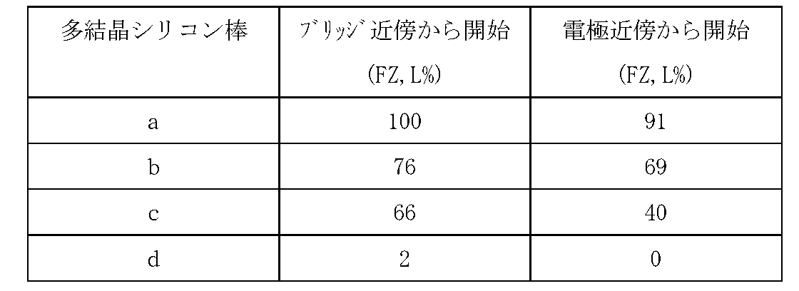
- Table 4 shows, for each of the four polycrystalline silicon rods (a, b, c, d), the values of FZ and L% when zone melting is started from the vicinity of the bridge, and the zone melting from the vicinity of the electrode It is the table
- the crystal evaluation method of the present invention can be organized as follows. That is, it is a crystal evaluation method of a polycrystalline silicon rod used as a raw material for producing single crystal silicon by the FZ method, and a plate-like shape having a main surface, a cross section perpendicular to the radial direction of the polycrystalline silicon rod grown by the Siemens method. A plurality of samples are collected at equal intervals in the radial direction, the crystal characteristic value of the plate-like sample is determined by measurement, and the crystal characteristic value is multiplied by the crystal amount (relative crystal amount) of the portion where the plate-like sample is collected. A crystal evaluation method of polycrystalline silicon rod, wherein the uniformity of the rod of polycrystalline silicon is evaluated by the evaluation value obtained.
- the evaluation method of “rotational symmetry” adopted in the present invention can be organized as follows. That is, the evaluation value is determined for two samples collected from the central axis of the polycrystalline silicon rod and the site at the target position, and the rotational symmetry is calculated by the following equation from the two evaluation values A and B obtained: A method of evaluating the crystal of a polycrystalline silicon rod, comprising the step of evaluating whether the average value in the axial direction of the rotational symmetry is 40% or more. 100- (
- the evaluation method of "rotational symmetry difference" adopted in the present invention can be organized as follows. That is, the evaluation values of the two samples taken from portions located on the same generatrix in the case where the distance in the radial direction from the central axis of the polycrystalline silicon rod is equal, and the polycrystalline silicon rod is cylindrically approximated Calculating a rotational symmetry difference from the obtained two evaluation values C and D by the following equation, and evaluating whether the average value of the rotational symmetry difference in the axial direction is 40% or less Crystal evaluation method of polycrystalline silicon rod provided. (
- Experimental Example 1 is an examination of the influence of the external shape of the polycrystalline silicon rod on FZ and L%. The examination results are shown in Table 5.
- the comparative example is a polycrystalline silicon rod as synthesized by the Siemens method, and the one in the example is formed by cylindrically grinding these polycrystalline silicon rods.
- the difference ⁇ D 1 between the maximum value D max and the minimum value D min of the diameter over the entire length is 3 mm or less, and is rotated about the central axis in the stretching direction of the polycrystalline silicon rod
- the difference ⁇ D 2 between the maximum value D max and the minimum value D min of the diameter of the substantially cylindrical virtual rotating body formed at that time is 6 mm or less.
- the ⁇ D 1 is larger than 3 mm
- the ⁇ D 2 is larger than 6 mm.
- one having a “rotational symmetry” of 40% or more is adopted as a polycrystalline silicon rod suitable as a raw material for producing single crystal silicon by the FZ method.
- the thing whose above-mentioned "rotational symmetry difference" is 40% or less is employ
- a pair of (two) silicon cores are assembled in an inverted U-shape via a bridge to form a polycrystal.
- a polycrystalline silicon rod taken from the leg of an inverted U-shaped polycrystalline silicon portion obtained by depositing silicon one end side of the polycrystalline silicon rod is in the vicinity of the bridge in the deposition furnace.
- the other end side is in the vicinity of the electrode in the deposition furnace, it is preferable to start the zone floating melting process from the vicinity of the bridge of the polycrystalline silicon rod.
- a technique for obtaining a polycrystalline silicon rod suitable as a raw material for producing single crystal silicon by the FZ method which is excellent in shape uniformity and crystal characteristic uniformity.
Landscapes
- Chemical & Material Sciences (AREA)
- Organic Chemistry (AREA)
- Crystallography & Structural Chemistry (AREA)
- Engineering & Computer Science (AREA)
- Materials Engineering (AREA)
- Metallurgy (AREA)
- Inorganic Chemistry (AREA)
- Physics & Mathematics (AREA)
- Immunology (AREA)
- Analytical Chemistry (AREA)
- Biochemistry (AREA)
- General Health & Medical Sciences (AREA)
- General Physics & Mathematics (AREA)
- Health & Medical Sciences (AREA)
- Pathology (AREA)
- Life Sciences & Earth Sciences (AREA)
- Electromagnetism (AREA)
- Silicon Compounds (AREA)
- Crystals, And After-Treatments Of Crystals (AREA)
- Analysing Materials By The Use Of Radiation (AREA)
Abstract
FZ法による単結晶シリコン製造用原料として用いられる多結晶シリコン棒の結晶評価に際し、成長方向(径方向)の結晶成長量を包含する新たな評価値(特性値×結晶量)を定義して、成長方向(径方向)の結晶特性の均一性評価を行う。具体的には、シーメンス法で育成された多結晶シリコン棒の径方向に垂直な断面を主面とする板状試料を前記径方向に等間隔に複数採取し、該板状試料の結晶特性値を測定により求め、該板状試料が採取された部位の結晶量(相対結晶量)を前記結晶特性値に乗じて得た評価値により、多結晶シリコンの棒の均一性を評価する。
Description
本発明は、多結晶シリコン棒の製造技術に関し、より詳細には、FZ法による単結晶シリコン製造用原料として好適な多結晶シリコン棒の製造技術に関する。
半導体デバイス等の製造に不可欠な単結晶シリコンは、CZ法やFZ法により結晶育成され、その際の原料として多結晶シリコン塊や多結晶シリコン棒が用いられる。このような多結晶シリコン材料は多くの場合、シーメンス法により製造される(特許文献1(特公昭37-18861号公報)等参照)。シーメンス法とは、トリクロロシランやモノシラン等のシラン原料ガスを加熱されたシリコン芯線に接触させることにより、該シリコン芯線の表面に多結晶シリコンをCVD(Chemical Vapor Deposition)法により気相成長(析出)させる方法である。
例えば、CZ法で単結晶シリコンを結晶育成する際には、石英ルツボ内に多結晶シリコン塊をチャージし、これを加熱溶融させたシリコン融液に種結晶を浸漬させて転位線を消滅させ、無転位化させた後に所定の直径となるまで徐々に径拡大させて、一定の速度で結晶の引上げが行われる。この時、シリコン融液中に未溶融の多結晶シリコンが残存していると、この未溶融多結晶片が対流により固液界面近傍を漂い、転位発生を誘発して結晶線を消失させてしまう原因となる。
特許文献2(特開2014-001096号公報)には、単結晶シリコン製造用原料として好適な多結晶シリコンを高い定量性と再現性で選別し、単結晶シリコンの安定的製造に寄与する技術を提供することを目的とした、多結晶シリコンの結晶配向度をX線回折法により評価する方法が開示されている。
特許文献2には、従来の目視観察では結晶粒が確認されない多結晶シリコンであっても、これを原料として単結晶シリコンを製造すると転位発生の誘発に起因する結晶線消失を生じる場合があるとの問題に鑑み、新たな手法として、多結晶シリコンの結晶配向度をX線回折法により評価するにあたり、採取した円板状試料をミラー指数面<hkl>からのブラッグ反射が検出される位置に配置し、スリットにより定められるX線照射領域が円板状試料の主面上をφスキャンするように円板状試料の中心を回転中心として回転角度φで面内回転させ、ミラー指数面<hkl>からのブラッグ反射強度の円板状試料の回転角度(φ)依存性を示すチャートを求め、該チャートからベースラインを求め、該ベースラインの回折強度値を結晶配向度の評価指標として用いる方法が提案されている。
そして、当該手法による評価結果に基づいて選択された多結晶シリコン棒乃至多結晶シリコン塊を用いて単結晶シリコンの育成を行うと、結晶線消失の発生が高い確率で防止できるとされている。
特に、上述のシリコン棒AやBのように、ミラー指数面<111>についての複数のベースライン回折強度値の最大値を最小値で除した値が1.5以下で、ミラー指数面<220>についての複数のベースライン回折強度値の最大値を最小値で除した値も1.9以下であり、且つ、何れの板状試料についても除算値(I<111>/I<220>)が2.5未満である多結晶シリコン棒は、単結晶シリコン育成用の原料として好適であるとの報告がある。
特許文献3(特開2013-217653号公報)にも、単結晶シリコン製造用原料として好適な多結晶シリコンを高い定量性と再現性で選別し、単結晶シリコンの安定的製造に寄与する技術を提供することを目的とした、多結晶シリコンの結晶配向度をX線回折法により評価する方法が開示されている。
具体的には、多結晶シリコン棒から採取された円板状試料について評価を行うとφスキャン・チャート中にピークが現れることがあり、このようなピークの本数が少ないほど、また、その半値幅が狭いほど、単結晶シリコン製造用の原料として好適である旨が記載されており、φスキャン・チャートに現れるピークの本数は、ミラー指数面<111>および<220>の何れについても、円板状試料の単位面積当たりの換算で24本/cm2以下であることが好ましいこと、また、円板状試料の半径をR0としたときに、ピーク半値幅にδL=21/2πR0/360を乗じて得られる値を不均質結晶粒径と定義付け、該不均質結晶粒径が何れも0.5mm未満のものを単結晶シリコン製造用原料として選択することが好ましいとの報告がなされている。
特許文献4(特開2014-031297号公報)にも、単結晶シリコン製造用原料として好適な多結晶シリコンを高い定量性と再現性で選別し、単結晶シリコンの安定的製造に寄与する技術を提供することを目的とした、単結晶シリコン製造用原料として用いる多結晶シリコン棒を選択するための方法が開示されている。
具体的には、多結晶シリコン棒から採取された板状試料の主面に電子線を照射して得られる電子後方散乱回折像を解析し、粒径が0.5μm以上の結晶粒が検出されない領域の総和面積が、電子線照射された面積全体の10%以下であること(条件1)、および、粒径が0.5μm以上で3μm未満の範囲にある結晶粒の個数が、検出された結晶粒の全体の45%以上であること(条件2)、を同時に満足する多結晶シリコン棒を単結晶シリコン製造用原料として選択する。係る多結晶シリコン棒を用いて単結晶シリコンの育成を行うと結晶線の消失が生じないため、単結晶シリコンの安定的製造が可能となるとの報告がなされている。
特許文献5(特開2014-034506号公報)にも、単結晶シリコン製造用原料として好適な多結晶シリコンを高い定量性と再現性で選別し、単結晶シリコンの安定的製造に寄与する技術を提供することを目的とした、単結晶シリコン製造用原料として用いる多結晶シリコン棒を選択するための方法が開示されている。
具体的には、化学成長法による析出で育成された多結晶シリコン棒の径方向に垂直な断面を主面とする板状試料を採取して、この板状試料の熱拡散率α(T)を測定し、標準試料の熱拡散率αR(T)と比較して、熱拡散率の比(α(T)/αR(T))に基づいて単結晶シリコン製造用の原料として好適な多結晶シリコン棒を選択する方法である。このようにして選択された多結晶シリコン棒を用いて単結晶シリコンの育成を行うと、結晶線の消失が生じないため、単結晶シリコンの安定的製造が可能となるとの報告がなされている。
これらの文献に開示の方法は、何れも、多結晶シリコン棒の成長方向(径方向)における特性値やその分布を評価するというものであるが、多結晶シリコン棒の成長方向(径方向)における回転対称性や、延伸方向(軸方向)における結晶の均一性等については評価の対象とされていない。
FZ法による単結晶シリコン製造用原料として用いられる多結晶シリコン棒においては、その成長方向(径方向)の諸特性の分布状態と同様に、延伸方向(軸方向)における諸特性の分布状態は重要なファクターである。ここで、結晶の特性とは、例えば、結晶生成量、結晶配向性、結晶粒径、結晶粒径、熱拡散率、熱伝導度などである。
これは、FZ法(帯域浮遊熔融法)により単結晶シリコンを製造する際には、多結晶シリコン棒を回転させながらゾーニングを行うためであるが、これまでは、延伸方向(軸方向)における結晶特性の均一性等については評価の対象とされてこなかった。
しかし、FZ法による単結晶シリコン製造用原料として好適な多結晶シリコン棒を得るためには、多結晶シリコン棒の全体としての「結晶特性の均一性」を高めること、すなわち、多結晶シリコン棒の成長方向(径方向)における結晶特性均一性だけではなく、延伸方向(軸方向)における結晶特性均一性も高める必要がある。
加えて、「結晶特性の均一性」だけではなく、多結晶シリコン棒の「形状均一性」も重要である。これは、多結晶シリコン棒の延伸方向(軸方向)における「形状均一性」が低いと、熱が均一に伝熱しないために、無転位状態にあることを示す晶癖線が消失する(有転位化する)ことがあるためである。
本発明は、このような事情に鑑みてなされたもので、その目的とするところは、形状均一性および結晶特性均一性に優れた、FZ法による単結晶シリコン製造用原料として好適な多結晶シリコン棒を得るための技術を提供することにある。
上記課題を解決するために、本発明に係る第1の態様の多結晶シリコン棒は、FZ法による単結晶シリコン製造用原料として用いられる多結晶シリコン棒であって、前記多結晶シリコン棒は全長が500mm以上であり、全長に渡っての直径の最大値Dmaxと最小値Dminの差ΔD1が3mm以下である。
例えば、前記多結晶シリコン棒の平均直径は300mm以下である。
本発明に係る第2の態様の多結晶シリコン棒は、FZ法による単結晶シリコン製造用原料として用いられる多結晶シリコン棒であって、前記多結晶シリコン棒は全長が500mm以上であり、前記多結晶シリコン棒の延伸方向の中心軸で回転させた際に形成される略円柱状の仮想回転体の直径の最大値Dmaxと最小値Dminの差ΔD2が6mm以下である。
例えば、前記多結晶シリコン棒の平均直径は300mm以下である。
本発明に係る第1の態様の多結晶シリコン棒の加工方法は、FZ法による単結晶シリコン製造用原料として用いられる多結晶シリコン棒の加工方法であって、前記多結晶シリコン棒はシーメンス法により育成された全長が500mm以上の多結晶シリコン棒であり、全長に渡っての直径の最大値Dmaxと最小値Dminの差ΔD1が3mm以下となるように、前記多結晶シリコン棒の側面を円筒研削する。
本発明に係る第2の態様の多結晶シリコン棒の加工方法は、FZ法による単結晶シリコン製造用原料として用いられる多結晶シリコン棒の加工方法であって、前記多結晶シリコン棒はシーメンス法により育成された全長が500mm以上の多結晶シリコン棒であり、該多結晶シリコン棒の延伸方向の中心軸で回転させた際に形成される略円柱状の仮想回転体の直径の最大値Dmaxと最小値Dminの差ΔD2が6mm以下となるように、前記多結晶シリコン棒の側面を円筒研削する。
本発明に係る多結晶シリコン棒の結晶評価方法は、FZ法による単結晶シリコン製造用原料として用いられる多結晶シリコン棒の結晶評価方法であって、シーメンス法で育成された多結晶シリコン棒の径方向に垂直な断面を主面とする板状試料を前記径方向に等間隔に複数採取し、該板状試料の結晶特性値を測定により求め、該板状試料が採取された部位の相対結晶量を前記結晶特性値に乗じて得た評価値により、多結晶シリコンの棒の均一性を評価する。
ある態様では、前記多結晶シリコン棒の中心軸と対象位置にある部位から採取した2つの試料について前記評価値を求め、得られた2つの評価値AおよびBから下式により回転対称性を算出し、該回転対称性の軸方向での平均値が40%以上であるか否かを評価するステップを備えている。
100-(|A-B|/(A+B)/2)×100
100-(|A-B|/(A+B)/2)×100
また、ある態様では、前記多結晶シリコン棒の中心軸からの径方向の距離が等しく、且つ、前記多結晶シリコン棒を円筒近似した場合の同一母線上に位置する部位から採取した2つの試料について前記評価値を求め、得られた2つの評価値CおよびDから下式により回転対称性差異を算出し、該回転対称性差異の軸方向での平均値が40%以下であるか否かを評価するステップを備えている。
(|C-D|/(C+D)/2)×100
(|C-D|/(C+D)/2)×100
上述の多結晶シリコン棒の結晶評価方法において、前記結晶特性は、例えば、結晶生成量、結晶配向性、結晶粒径、熱拡散率、熱伝導度の何れかである。
本発明に係るFZ単結晶シリコンの製造方法は、多結晶シリコン棒を原料としたFZ単結晶シリコンの製造方法であって、前記多結晶シリコン棒は、1対(2本)のシリコン芯線をブリッジを介して逆U字型に組んで多結晶シリコンを析出させて得られた逆U字型の多結晶シリコン部の脚部から採取された多結晶シリコン棒であり、前記多結晶シリコン棒の一方端部側を析出炉内でのブリッジ近傍部とし、他方端部側を析出炉内での電極近傍部としたときに、帯域浮遊熔融工程を、前記多結晶シリコン棒のブリッジ近傍部より開始することを特徴とする。
本発明においては、「特性値×相対結晶量」なる新たな評価値を導入し、これに基づき、「回転対称性」が40%以上のものを、FZ法による単結晶シリコン製造用原料として好適な多結晶シリコン棒として採用する。また、「回転対称性差異」が40%以下のものを、FZ法による単結晶シリコン製造用原料として好適な多結晶シリコン棒として採用する。
本発明によれば、形状均一性および結晶特性均一性に優れた、FZ法による単結晶シリコン製造用原料として好適な多結晶シリコン棒を得るための技術が提供される。
本発明者らは、FZ法による単結晶シリコン製造用原料として好適な多結晶シリコン棒は、多結晶シリコン棒の延伸方向(軸方向)における「形状均一性」が高いこと、また、多結晶シリコン棒の成長方向(径方向)における結晶特性均一性だけではなく延伸方向(軸方向)における結晶特性均一性も高いことが必要であるとの認識のもとに誠意検討した結果、本発明を成すに至った。以下に、図面を参照して、本発明を実施するための形態について説明する。
[形状均一性]
シーメンス法により得られた直後の多結晶シリコン棒の断面は、完全な真円ではなく僅かに楕円であることが多い。加えて、延伸方向(軸方向)に渡る断面形状は、多くの場合、部位ごとに異なっている。つまり、シーメンス法により育成されたままの多結晶シリコン棒は、延伸方向(軸方向)において「形状均一」ではない。
シーメンス法により得られた直後の多結晶シリコン棒の断面は、完全な真円ではなく僅かに楕円であることが多い。加えて、延伸方向(軸方向)に渡る断面形状は、多くの場合、部位ごとに異なっている。つまり、シーメンス法により育成されたままの多結晶シリコン棒は、延伸方向(軸方向)において「形状均一」ではない。
本発明者らの検討によれば、多結晶シリコン棒の延伸方向(軸方向)における「形状均一性」が低いと、これをFZ法による単結晶シリコン製造用原料として用いた場合に、無転位状態にあることを示す晶癖線が消失する(有転位化する)ことがある。これは、高周波加熱による融解、対流、固化の連続状態変化において熱の伝導が一定に行われないためである。
そこで、多結晶シリコン棒の断面の「真円性」がどの程度であればFZ法による単結晶シリコン製造用原料として好適であるのか、さらに、多結晶シリコン棒の延伸方向の中心軸で回転させた際に形成される略円柱状の仮想回転体の直径の最大値と最小値の差がどの程度であればFZ法による単結晶シリコン製造用原料として好適であるのかについて検討を行った。なお、多結晶シリコン棒は全長が500mm以上で平均直径が300mm以下(5~12インチ径)のもので評価を行い、「好適」であることの判断は、晶癖線の消失の有無により行った。
その結果、下記の条件を満足する多結晶シリコン棒を用いてFZ法により単結晶シリコンを製造すると、晶癖線の消失が認められないとの知見を得た。
すなわち、多結晶シリコン棒の断面の「真円性」についてみると、全長に渡っての直径の最大値Dmaxと最小値Dminの差ΔD1が3mm以下であることが条件となる。
また、多結晶シリコン棒の延伸方向の中心軸で回転させた際に形成される略円柱状の仮想回転体の直径の最大値と最小値の差についてみると、最大値Dmaxと最小値Dminの差ΔD2が6mm以下であることが条件となる。なお、この最大値Dmaxと最小値Dminの差ΔD2は、実際のFZプロセス時に多結晶シリコン棒を把持して回転させる際の、径方向の変動幅に相当する。
つまり、本発明に係る多結晶シリコン棒は、FZ法による単結晶シリコン製造用原料として用いられる多結晶シリコン棒であって、前記多結晶シリコン棒は全長が500mm以上であり、全長に渡っての直径の最大値Dmaxと最小値Dminの差ΔD1が3mm以下である。
シーメンス法により得られた直後の多結晶シリコン棒の形状が上記条件を満足しない場合には、多結晶シリコン棒の側面を円筒研削することにより成形することになる。
すなわち、本発明に係る多結晶シリコン棒の加工方法は、FZ法による単結晶シリコン製造用原料として用いられる多結晶シリコン棒の加工方法であって、前記多結晶シリコン棒はシーメンス法により育成された全長が500mm以上の多結晶シリコン棒であり、全長に渡っての直径の最大値Dmaxと最小値Dminの差ΔD1が3mm以下となるように、前記多結晶シリコン棒の側面を円筒研削する。
また、本発明に係る多結晶シリコン棒は、FZ法による単結晶シリコン製造用原料として用いられる多結晶シリコン棒であって、前記多結晶シリコン棒は全長が500mm以上であり、前記多結晶シリコン棒の延伸方向の中心軸で回転させた際に形成される略円柱状の仮想回転体の直径の最大値Dmaxと最小値Dminの差ΔD2が6mm以下である。
上述したように、シーメンス法により得られた直後の多結晶シリコン棒の形状が上記条件を満足しない場合には、多結晶シリコン棒の側面を円筒研削することにより成形することになる。
すなわち、本発明に係る多結晶シリコン棒の加工方法は、FZ法による単結晶シリコン製造用原料として用いられる多結晶シリコン棒の加工方法であって、前記多結晶シリコン棒はシーメンス法により育成された全長が500mm以上の多結晶シリコン棒であり、該多結晶シリコン棒の延伸方向の中心軸で回転させた際に形成される略円柱状の仮想回転体の直径の最大値Dmaxと最小値Dminの差ΔD2が6mm以下となるように、前記多結晶シリコン棒の側面を円筒研削する。
[結晶特性均一性]
上述したように、特許文献2~5に開示された評価方法は何れも、多結晶シリコン棒の成長方向(径方向)の結晶特性値(若しくはその分布)についてのものである。しかし、多結晶シリコン棒は円柱状であり、延伸方向(軸方向)の結晶特性値(若しくはその分布)も考慮しないと、FZ操作における晶癖線の消失を抑制するためには十分ではない。
上述したように、特許文献2~5に開示された評価方法は何れも、多結晶シリコン棒の成長方向(径方向)の結晶特性値(若しくはその分布)についてのものである。しかし、多結晶シリコン棒は円柱状であり、延伸方向(軸方向)の結晶特性値(若しくはその分布)も考慮しないと、FZ操作における晶癖線の消失を抑制するためには十分ではない。
また、FZ法により単結晶シリコンを製造するに際しては、多結晶シリコン棒を把持して回転させながら熔解、帯域熔融、固化により単結晶成長を行うため、多結晶シリコン棒の成長方向(径方向)の結晶特性値(若しくはその分布)を評価するに際しても、その回転対称性を評価することが必要である。
ここで、多結晶シリコン棒は円柱状であるから、中心から成長距離dにある多結晶量はdの2乗に比例することとなり、中心側ほど多結晶量は少なく、外側に向かうほど多結晶量は多くなる。本発明者らは、FZプロセス時の熱安定性、熱負荷、熔融内部における融液の対流に影響を与えるのは、単なる結晶特性値ではなく、この結晶特性値に寄与している多結晶量を乗じた評価値(特性値×結晶量)であると考え、本発明を成すに至った。つまり、本発明者らは、成長方向(径方向)の結晶成長量を包含する新たな評価値(特性値×結晶量)を定義して、成長方向(径方向)の結晶特性の均一性評価を行うこととした。なお、ここで、本発明において重要な点は、試料採取位置における相対的な多結晶量であるから、上記「結晶量」は絶対値である必要はなく、「相対結晶量」であればよい。その意味で、上記「評価値」は、特性値×「相対結晶量」であってよい。
延伸方向(軸方向)の結晶特性の均一性評価も同様であって、上記評価値(特性値×相対結晶量)により評価することとなる。
上述の評価値(特性値×相対結晶量)とは、例えば、下記のようなものとなる。
図1は、特性値評価に供する試料の採取法の一例を説明するための図で、この図に示した例では、シーメンス法でシリコン芯線1上への析出により育成させた直径が約150mmの多結晶シリコン棒10のブリッジ近傍部、すなわち炉内で最も高い位置にあった部位の側面側から、直径が概ね20mmで長さが概ね750mmのロッド11を、多結晶シリコン棒の軸方向と垂直にくり抜いて採取し、10mm間隔で、厚みが概ね2mmの板状試料12を、全部で16枚採取する。そして、これらの板状試料12のそれぞれにつき、ミラー指数面<111>および<220>からのブラッグ反射強度を求める。
同様に、多結晶シリコン棒10の電極近傍部、すなわち炉内で最も低い位置にあった部位の側面側から、直径が概ね20mmで長さが概ね750mmのロッド11を、多結晶シリコン棒の軸方向と垂直にくり抜いて採取し、10mm間隔で、厚みが概ね2mmの板状試料12を、全部で16枚採取する。そして、これらの板状試料12のそれぞれにつき、ミラー指数面<111>および<220>からのブラッグ反射強度を求める。
本発明では、これらの多結晶シリコン棒の各部位の成長方向(径方向)の対称性を、結晶特性値としての回折強度値と相対結晶量の積で評価する。ここで、当該評価値を算出するための「相対結晶量」は、先ず、各板状試料を採取した部位の中心からの距離dを2乗してd2を求める。そして、近接して採取された板状試料のd2値の差であるΔd2を求める。
表1は、ブリッジ近傍部(炉内で最も高い位置にあった部位)から採取した計16枚の板状試料(SPL)の採取位置(中心からの距離:d)、当該dを2乗した値d2、隣接する板状試料のd2値との差分Δd2、測定値であるミラー指数面<111>および<220>からのブラッグ反射強度(I<111>およびI<220>)、これらI<111>およびI<220>に上記差分Δd2を乗じて得られた評価値(I<111>×Δd2およびI<220>×Δd2)を纏めた表である。なお、「回転対称性」の平均値は、<111>につき88%であり、<220>につき89%である。

表2は、電極近傍部(炉内で最も低い位置にあった部位)から採取した計16枚の板状試料(SPL)についての採取位置(d)、当該dを2乗した値d2、隣接する板状試料のd2値との差分Δd2、測定値であるミラー指数面<111>および<220>からのブラッグ反射強度(I<111>およびI<220>)、これらI<111>およびI<220>に上記差分Δd2を乗じて得られた評価値(I<111>×Δd2およびI<220>×Δd2)を纏めた表である。なお、「回転対称性」の平均値は、<111>につき91%であり、<220>につき84%である。

図2は、これら計32枚の板状試料から得られた評価値をグラフ化した図である。
表1および表2中の「回転対称性」は、中心軸から左右対称の等距離にある板状試料から得られた評価値の差を、下記の手順で%表示した値である。例えば、表1において、板状試料6は中心からの距離d=2cmであるから、これと左右対称の等距離にある板状試料は試料11であり、ミラー指数面<111>についての評価値でみると、試料6のそれは25,762であり、試料11のそれは28,787であるから、その差は3,025となる。この値3,025を上記評価値の平均27,275で割って%表示した値は11.1%となる。この11.1%を100%から引いた値が88.9%となり、この値をもって「回転対称性」としている。
採取位置が高さ方向で異なる試料同士についても同様の計算を行い、多結晶シリコン棒の軸方向(炉内での高さ方向)での差の程度を評価する。例えば、表1に示した板状試料6は中心からの距離d=2cmであるから、これに対応する試料は表2中の試料6となる。これらの試料のミラー指数面<111>についての評価値でみると、表1中の試料6のそれは25,762であり、表2中の試料のそれは26,906であるから、その差は1,144となる。この値1,144を上記評価値の平均26,334で割って%表示した値は4.3%となる。この4.3%をもって軸方向での「回転対称性差異」としている。
表3は、上述の演算により求めた軸方向での「回転対称性差異」を纏めた表である。なお、「回転対称性差異」の平均値は、<111>につき10%であり、<220>につき17%である。

本発明においては、上述の「回転対称性」が40%以上のものを、FZ法による単結晶シリコン製造用原料として好適な多結晶シリコン棒として採用する。また、上述の「回転対称性差異」が40%以下のものを、FZ法による単結晶シリコン製造用原料として好適な多結晶シリコン棒として採用する。
「回転対称性差異」が40%以下との基準は、実際のFZ、L%と特性値から算出した評価値の実績値との関係から、FZ、L%の値が66%以上得られる時の評価値の違いの値を求めると40%であったことによる。なお、この判断に際してのn数は十分であり、統計的に計算される相関関係が1%の危険率から計算される判定基準に対して、高度に有意な相関関係が認められると判断した。
ここで、「FZ、L%」とは、多結晶シリコンの棒の長さを100としたときに、1回のFZ操作で結晶成長させて得られた結晶シリコンに備わっている晶僻線が完全な状態で存在している多結晶シリコン棒の長さを%で表したものである。不完全な晶僻線としては、晶僻線の消失はもとより、晶僻線の乱れや曲がりなどがある。本明細書で言うFZ、L%は全て、1回のFZ操作で得られる値であり、複数回のFZ操作により得られる値ではない。これは、2回以上のFZ操作を行うことは、生産性の低下を招くためであり、本発明では対象としない。
FZ、L%の値は必ずしも100%であることは必要ないが、より高いものが好ましく、その下限値は、生産性を考慮すると、60~70%程度であり、それ以下は事実上、使用出来ない。
上述の結晶特性がどのようなものであるかについての特別な制約はないが、例えば、結晶生成量、結晶配向性、結晶粒径、熱拡散率、熱伝導度などの物性値を例示することができ、それらの特性値の分布を結晶特性として採用することとしてもよい。
X線回折法を用いて特定のミラー指数面からの回折強度を測定する手順は、特許文献2や3に記載されているものと同様でよい。
また、結晶粒径や結晶粒径分布を評価する手順は、特許文献4に記載されているものと同様でよい。
さらに、熱拡散率および熱伝導率を評価する手順は、特許文献5に記載されているものと同様でよい。
「回転対称性」は、一般に、ブリッジ近傍よりも、電極近傍において低い傾向がある。この傾向は、多結晶シリコン析出時の諸条件を変えても同様である。炉内での低い位置にある結晶部位は、反応プロセス中に冷却されているカーボン製の電極に近いため、炉内での高い位置にある結晶部位に比べて、CVD温度が低下していることが考えられる。
この現象はシーメンス法の根本的な空間構造配置、ガス流分布を変えない限りは解決しないため、カーボン電極位置から一定の距離分を切り捨てる対策化を行うと、FZ用のシリコン棒の長さを短くすることに至ってしまう。どの程度の距離を確保するかは、結晶の高さ方向の均一性を指針に決定する必要が、ここにある。
軸方向の均一性を確保するために反応炉を長めに改造し、均熱部の長さを長くする方法も考えられるが、その状況下でもカーボン電極の近傍の温度低下は回避できず、一定割合で結晶の不均一性部分が発生してしまう。
この様に、多結晶シリコン棒の結晶特性の、炉内での高さ方向での部位依存性については、高い位置から低い位置に向かって徐々に結晶の均一性が低下して行くことがわかってきた。従って、多結晶シリコン棒としての全体の評価値把握するためには、多結晶シリコン棒の両端部位から採取した試料を評価する必要が生じる。
両端部位の評価を行えば、その中間領域は、これら2箇所の評価値の範囲内にあるであろうから、敢えてその他の領域を評価することは必要ない。つまり、高さ方向の2箇所の評価により、多結晶シリコン棒全体としての評価値が定まり、同時に、棒内の大凡のプロファイルも把握される。本発明は、特許文献2~5に開示されたような、成長方向(径方向)の単なる物性測定方法とは異なり、径方向の結晶量をも考慮した新たな評価値を導入し、更に、軸方向での結晶の(回転)対称性についても考慮した評価方法である。
本発明者らの行った実験によれば、上述の手法で評価した「回転対称性」が40%以上のものをFZ法による単結晶シリコン製造用原料として用いると、晶僻線の消失が認めらない長さ領域の割合が66%の単結晶インゴットが得られる。このような多結晶シリコン棒は、何れも、上述の「回転対称性差異」が40%以下のものであった。つまり、「回転対称性差異」が40%以下のものをFZ法による単結晶シリコン製造用原料として用いると、晶僻線の消失が認めらない長さ領域の割合が66%の単結晶インゴットが得られる。
また、一般に、ブリッジ近傍に比べてカーボン電極近傍の結晶の均一性は低いため、FZ法による単結晶シリコン製造プロセスにおいて帯域熔融を開始する際には、ブリッジ近傍部から開始した方が晶僻線は消失し難い。この理由として考えられることは、晶僻線は、一度生成すると多少の変動があっても、そのまま帯域熔融されて行く継続性の傾向があり、許容範囲外の変動があった場合にも消失するためと考えられる。
このような理由により、カーボン電極近傍部から帯域熔融を開始すると、帯域熔融をしている途中で、晶僻線が消失する可能性が高くなり、ブリッジ近傍部から開始するより不利となる。そのため、FZ用として帯域熔融プロセスは、ブリッジ近傍部から開始することが望ましい。
表4は、4本の多結晶シリコン棒(a、b、c、d)のそれぞれにつき、ブリッジ近傍部から帯域熔融を開始した場合のFZ、L%の値と、電極近傍部から帯域熔融を開始した場合のFZ、L%の値を比較して示した表である。
本発明の結晶評価方法は、下記のように整理できる。すなわち、FZ法による単結晶シリコン製造用原料として用いられる多結晶シリコン棒の結晶評価方法であって、シーメンス法で育成された多結晶シリコン棒の径方向に垂直な断面を主面とする板状試料を前記径方向に等間隔に複数採取し、該板状試料の結晶特性値を測定により求め、該板状試料が採取された部位の結晶量(相対結晶量)を前記結晶特性値に乗じて得た評価値により、多結晶シリコンの棒の均一性を評価する、多結晶シリコン棒の結晶評価方法。
また、本発明で採用する「回転対称性」の評価手法は、下記のように整理できる。すなわち、前記多結晶シリコン棒の中心軸と対象位置にある部位から採取した2つの試料について前記評価値を求め、得られた2つの評価値AおよびBから下式により回転対称性を算出し、該回転対称性の軸方向での平均値が40%以上であるか否かを評価するステップを備えている、多結晶シリコン棒の結晶評価方法。
100-(|A-B|/(A+B)/2)×100
100-(|A-B|/(A+B)/2)×100
さらに、本発明で採用する「回転対称性差異」の評価手法は、下記のように整理できる。すなわち、前記多結晶シリコン棒の中心軸からの径方向の距離が等しく、且つ、前記多結晶シリコン棒を円筒近似した場合の同一母線上に位置する部位から採取した2つの試料について前記評価値を求め、得られた2つの評価値CおよびDから下式により回転対称性差異を算出し、該回転対称性差異の軸方向での平均値が40%以下であるか否かを評価するステップを備えている、多結晶シリコン棒の結晶評価方法。
(|C-D|/(C+D)/2)×100
(|C-D|/(C+D)/2)×100
以下に、実験例(実施例および比較例)を示す。
[実験例1]
実験例1は、多結晶シリコン棒の外形形状がFZ,L%に及ぼす影響についての検討である。その検討結果を表5に示す。比較例はシーメンス法により合成したままの多結晶シリコン棒であり、実施例のものは、これらの多結晶シリコン棒を円筒研削して成形したものである。
実験例1は、多結晶シリコン棒の外形形状がFZ,L%に及ぼす影響についての検討である。その検討結果を表5に示す。比較例はシーメンス法により合成したままの多結晶シリコン棒であり、実施例のものは、これらの多結晶シリコン棒を円筒研削して成形したものである。
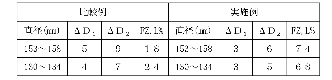
実施例のものは何れも、全長に渡っての直径の最大値Dmaxと最小値Dminの差ΔD1が3mm以下であり、且つ、多結晶シリコン棒の延伸方向の中心軸で回転させた際に形成される略円柱状の仮想回転体の直径の最大値Dmaxと最小値Dminの差ΔD2が6mm以下である。一方、比較例のものは何れも、上記ΔD1が3mmより大きく、ΔD2も6mmより大きい。
そして、実施例のものは何れも、FZ,L%が66を超えているのに対し、比較例のものは何れも、これを大きく下回るFZ,L%でしかない。
[実験例2]
実験例2の結果は、表1~3に示したものである。
実験例2の結果は、表1~3に示したものである。
既に述べたとおり、本発明においては、「回転対称性」が40%以上のものを、FZ法による単結晶シリコン製造用原料として好適な多結晶シリコン棒として採用する。また、上述の「回転対称性差異」が40%以下のものを、FZ法による単結晶シリコン製造用原料として好適な多結晶シリコン棒として採用する。
[実験例3]
実験例3では、FZ,L%の異なる5本の多結晶シリコン棒(FZ,L%=100、76、66、52、2)のそれぞれの、ブリッジ近傍から採取した試料と電極近傍から採取した試料の回転対称性(平均値)および回転対称性差異(平均値)を調べた。なお、この実施例では、評価値を求める際の結晶特性として、ラー指数面<111>および<220>からのブラッグ反射強度を採用した。表6に、その結果を纏めた。
実験例3では、FZ,L%の異なる5本の多結晶シリコン棒(FZ,L%=100、76、66、52、2)のそれぞれの、ブリッジ近傍から採取した試料と電極近傍から採取した試料の回転対称性(平均値)および回転対称性差異(平均値)を調べた。なお、この実施例では、評価値を求める際の結晶特性として、ラー指数面<111>および<220>からのブラッグ反射強度を採用した。表6に、その結果を纏めた。
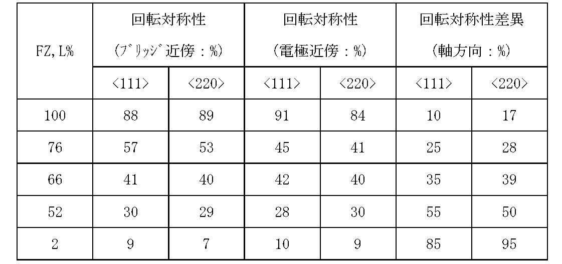
この表に纏めた結果に依れば、回転対称性の軸方向での平均値が40%以上であり、回転対称性差異の軸方向での平均値が40%以下である場合には、FZ,L%は66%以上となっている。
[実験例4]
実験例4でも、FZ,L%の異なる5本の多結晶シリコン棒(FZ,L%=100、76、66、52、2)のそれぞれの、ブリッジ近傍から採取した試料と電極近傍から採取した試料の回転対称性(平均値)および回転対称性差異(平均値)を調べた。なお、この実施例では、評価値を求める際の結晶特性として、ミラー指数面<111>および<220>の配向性を採用することとし、具体的には、ミラー指数面<111>および<220>からの回折強度の面積比率(%)を採用した。表7に、その結果を纏めた。
実験例4でも、FZ,L%の異なる5本の多結晶シリコン棒(FZ,L%=100、76、66、52、2)のそれぞれの、ブリッジ近傍から採取した試料と電極近傍から採取した試料の回転対称性(平均値)および回転対称性差異(平均値)を調べた。なお、この実施例では、評価値を求める際の結晶特性として、ミラー指数面<111>および<220>の配向性を採用することとし、具体的には、ミラー指数面<111>および<220>からの回折強度の面積比率(%)を採用した。表7に、その結果を纏めた。

この表に纏めた結果においても、回転対称性の軸方向での平均値が40%以上であり、回転対称性差異の軸方向での平均値が40%以下である場合には、FZ,L%は66%以上となっている。
[実験例5]
実験例5でも、FZ,L%の異なる5本の多結晶シリコン棒(FZ,L%=100、76、66、52、2)のそれぞれの、ブリッジ近傍から採取した試料と電極近傍から採取した試料の回転対称性(平均値)および回転対称性差異(平均値)を調べた。なお、この実施例では、評価値を求める際の結晶特性として、EBSD法で測定した平均粒径分布を採用することとした。表8に、その結果を纏めた。
実験例5でも、FZ,L%の異なる5本の多結晶シリコン棒(FZ,L%=100、76、66、52、2)のそれぞれの、ブリッジ近傍から採取した試料と電極近傍から採取した試料の回転対称性(平均値)および回転対称性差異(平均値)を調べた。なお、この実施例では、評価値を求める際の結晶特性として、EBSD法で測定した平均粒径分布を採用することとした。表8に、その結果を纏めた。

この表に纏めた結果に依れば、回転対称性の軸方向での平均値が40%以上であり、回転対称性差異の軸方向での平均値が40%以下である場合には、FZ,L%は66%以上となっている。
[実験例6]
実験例6でも、FZ,L%の異なる5本の多結晶シリコン棒(FZ,L%=100、76、66、52、2)のそれぞれの、ブリッジ近傍から採取した試料と電極近傍から採取した試料の回転対称性(平均値)および回転対称性差異(平均値)を調べた。なお、この実施例では、評価値を求める際の結晶特性として、熱拡散率を採用することとした。なお、熱伝導率は、熱拡散率に密度と比熱を乗じたものであるため、両者の値には差がない。表9に、その結果を纏めた。
実験例6でも、FZ,L%の異なる5本の多結晶シリコン棒(FZ,L%=100、76、66、52、2)のそれぞれの、ブリッジ近傍から採取した試料と電極近傍から採取した試料の回転対称性(平均値)および回転対称性差異(平均値)を調べた。なお、この実施例では、評価値を求める際の結晶特性として、熱拡散率を採用することとした。なお、熱伝導率は、熱拡散率に密度と比熱を乗じたものであるため、両者の値には差がない。表9に、その結果を纏めた。

この表に纏めた結果に依れば、回転対称性の軸方向での平均値が40%以上であり、回転対称性差異の軸方向での平均値が40%以下である場合には、FZ,L%は66%以上となっている。
[実験例7]
実験例7では、1対(2本)のシリコン芯線をブリッジを介して逆U字型に組んで多結晶シリコンを析出させ、その両脚部から採取された各1本(計2本)の多結晶シリコン棒を用い、一方(多結晶シリコン棒)はブリッジ近傍部からFZプロセスを開始し、他方(多結晶シリコン棒)は電極近傍部からFZプロセスを開始し、得られた単結晶シリコンのFZ,L%を比較した。なお、実験に用いた多結晶シリコンは、A~Dの4つの異なるシーメンスプロセスで育成されたものである。その結果を表10に示す。
実験例7では、1対(2本)のシリコン芯線をブリッジを介して逆U字型に組んで多結晶シリコンを析出させ、その両脚部から採取された各1本(計2本)の多結晶シリコン棒を用い、一方(多結晶シリコン棒)はブリッジ近傍部からFZプロセスを開始し、他方(多結晶シリコン棒)は電極近傍部からFZプロセスを開始し、得られた単結晶シリコンのFZ,L%を比較した。なお、実験に用いた多結晶シリコンは、A~Dの4つの異なるシーメンスプロセスで育成されたものである。その結果を表10に示す。

この表に纏めた結果に依れば、本来は同質の多結晶シリコン棒であっても、ブリッジ近傍部からFZプロセスを開始した方が、電極近傍部からFZプロセスを開始する場合よりも、FZ,L%は高い値を示している。
よって、多結晶シリコン棒を原料としたFZ単結晶シリコンの製造をするに際しては、多結晶シリコン棒として、1対(2本)のシリコン芯線をブリッジを介して逆U字型に組んで多結晶シリコンを析出させて得られた逆U字型の多結晶シリコン部の脚部から採取された多結晶シリコン棒を用いる場合、多結晶シリコン棒の一方端部側を析出炉内でのブリッジ近傍部とし、他方端部側を析出炉内での電極近傍部としたときに、帯域浮遊熔融工程を、多結晶シリコン棒のブリッジ近傍部より開始することが好ましい。
本発明によれば、形状均一性および結晶特性均一性に優れた、FZ法による単結晶シリコン製造用原料として好適な多結晶シリコン棒を得るための技術が提供される。
1 シリコン芯線
10 多結晶シリコン棒
11 ロッド
12 板状試料
10 多結晶シリコン棒
11 ロッド
12 板状試料
Claims (11)
- FZ法による単結晶シリコン製造用原料として用いられる多結晶シリコン棒であって、
前記多結晶シリコン棒は全長が500mm以上であり、
全長に渡っての直径の最大値Dmaxと最小値Dminの差ΔD1が3mm以下である、多結晶シリコン棒。 - 前記多結晶シリコン棒の平均直径が300mm以下である、請求項1に記載の多結晶シリコン棒。
- FZ法による単結晶シリコン製造用原料として用いられる多結晶シリコン棒であって、
前記多結晶シリコン棒は全長が500mm以上であり、
前記多結晶シリコン棒の延伸方向の中心軸で回転させた際に形成される略円柱状の仮想回転体の直径の最大値Dmaxと最小値Dminの差ΔD2が6mm以下である、多結晶シリコン棒。 - 前記多結晶シリコン棒の平均直径が300mm以下である、請求項3に記載の多結晶シリコン棒。
- FZ法による単結晶シリコン製造用原料として用いられる多結晶シリコン棒の加工方法であって、
前記多結晶シリコン棒はシーメンス法により育成された全長が500mm以上の多結晶シリコン棒であり、
全長に渡っての直径の最大値Dmaxと最小値Dminの差ΔD1が3mm以下となるように、前記多結晶シリコン棒の側面を円筒研削する、多結晶シリコン棒の加工方法。 - FZ法による単結晶シリコン製造用原料として用いられる多結晶シリコン棒の加工方法であって、
前記多結晶シリコン棒はシーメンス法により育成された全長が500mm以上の多結晶シリコン棒であり、
該多結晶シリコン棒の延伸方向の中心軸で回転させた際に形成される略円柱状の仮想回転体の直径の最大値Dmaxと最小値Dminの差ΔD2が6mm以下となるように、前記多結晶シリコン棒の側面を円筒研削する、多結晶シリコン棒の加工方法。 - FZ法による単結晶シリコン製造用原料として用いられる多結晶シリコン棒の結晶評価方法であって、
シーメンス法で育成された多結晶シリコン棒の径方向に垂直な断面を主面とする板状試料を前記径方向に等間隔に複数採取し、該板状試料の結晶特性値を測定により求め、該板状試料が採取された部位の相対結晶量を前記結晶特性値に乗じて得た評価値により、多結晶シリコンの棒の均一性を評価する、多結晶シリコン棒の結晶評価方法。 - 前記多結晶シリコン棒の中心軸と対象位置にある部位から採取した2つの試料について前記評価値を求め、得られた2つの評価値AおよびBから下式により回転対称性を算出し、該回転対称性の軸方向での平均値が40%以上であるか否かを評価するステップを備えている、請求項7に記載の、多結晶シリコン棒の結晶評価方法。
100-(|A-B|/(A+B)/2)×100 - 前記多結晶シリコン棒の中心軸からの径方向の距離が等しく、且つ、前記多結晶シリコン棒を円筒近似した場合の同一母線上に位置する部位から採取した2つの試料について前記評価値を求め、得られた2つの評価値CおよびDから下式により回転対称性差異を算出し、該回転対称性差異の軸方向での平均値が40%以下であるか否かを評価するステップを備えている、請求項7に記載の、多結晶シリコン棒の結晶評価方法。
(|C-D|/(C+D)/2)×100 - 前記結晶特性は、結晶生成量、結晶配向性、結晶粒径、熱拡散率、熱伝導度の何れかである、請求項7~9の何れか1項に記載の多結晶シリコン棒の結晶評価方法。
- 多結晶シリコン棒を原料としたFZ単結晶シリコンの製造方法であって、
前記多結晶シリコン棒は、1対(2本)のシリコン芯線をブリッジを介して逆U字型に組んで多結晶シリコンを析出させて得られた逆U字型の多結晶シリコン部の脚部から採取された多結晶シリコン棒であり、
前記多結晶シリコン棒の一方端部側を析出炉内でのブリッジ近傍部とし、他方端部側を析出炉内での電極近傍部としたときに、
帯域浮遊熔融工程を、前記多結晶シリコン棒のブリッジ近傍部より開始する、FZ単結晶シリコンの製造方法。
Priority Applications (3)
| Application Number | Priority Date | Filing Date | Title |
|---|---|---|---|
| US15/537,968 US10800659B2 (en) | 2014-12-25 | 2015-12-09 | Polycrystalline silicon rod, processing method for polycrystalline silicon rod, method for evaluating polycrystalline silicon rod, and method for producing FZ single crystal silicon |
| DE112015005391.3T DE112015005391T5 (de) | 2014-12-25 | 2015-12-09 | Polykristalliner Siliciumstab, Bearbeitungsverfahren für polykristalline Siliciumstäbe, Verfahren zum Bewerten polykristalliner Siliciumstäbe und Verfahren zum Herstellen monokristallinen FZ-Siliciums |
| US17/012,418 US11167994B2 (en) | 2014-12-25 | 2020-09-04 | Polycrystalline silicon rod, processing method for polycrystalline silicon rod, method for evaluating polycrystalline silicon rod, and method for producing FZ single crystal silicon |
Applications Claiming Priority (2)
| Application Number | Priority Date | Filing Date | Title |
|---|---|---|---|
| JP2014263296A JP6345108B2 (ja) | 2014-12-25 | 2014-12-25 | 多結晶シリコン棒、多結晶シリコン棒の加工方法、多結晶シリコン棒の結晶評価方法、および、fz単結晶シリコンの製造方法 |
| JP2014-263296 | 2014-12-25 |
Related Child Applications (2)
| Application Number | Title | Priority Date | Filing Date |
|---|---|---|---|
| US15/537,968 A-371-Of-International US10800659B2 (en) | 2014-12-25 | 2015-12-09 | Polycrystalline silicon rod, processing method for polycrystalline silicon rod, method for evaluating polycrystalline silicon rod, and method for producing FZ single crystal silicon |
| US17/012,418 Division US11167994B2 (en) | 2014-12-25 | 2020-09-04 | Polycrystalline silicon rod, processing method for polycrystalline silicon rod, method for evaluating polycrystalline silicon rod, and method for producing FZ single crystal silicon |
Publications (1)
| Publication Number | Publication Date |
|---|---|
| WO2016103608A1 true WO2016103608A1 (ja) | 2016-06-30 |
Family
ID=56149677
Family Applications (1)
| Application Number | Title | Priority Date | Filing Date |
|---|---|---|---|
| PCT/JP2015/006142 Ceased WO2016103608A1 (ja) | 2014-12-25 | 2015-12-09 | 多結晶シリコン棒、多結晶シリコン棒の加工方法、多結晶シリコン棒の結晶評価方法、および、fz単結晶シリコンの製造方法 |
Country Status (4)
| Country | Link |
|---|---|
| US (2) | US10800659B2 (ja) |
| JP (1) | JP6345108B2 (ja) |
| DE (1) | DE112015005391T5 (ja) |
| WO (1) | WO2016103608A1 (ja) |
Families Citing this family (1)
| Publication number | Priority date | Publication date | Assignee | Title |
|---|---|---|---|---|
| JP7128124B2 (ja) * | 2019-01-18 | 2022-08-30 | 信越化学工業株式会社 | 多結晶シリコン棒、多結晶シリコンロッドおよびその製造方法 |
Citations (6)
| Publication number | Priority date | Publication date | Assignee | Title |
|---|---|---|---|---|
| JPS53108029A (en) * | 1977-03-03 | 1978-09-20 | Komatsu Mfg Co Ltd | Method of making high purity silicon having uniform shape |
| JPH09165296A (ja) * | 1995-12-15 | 1997-06-24 | Komatsu Electron Metals Co Ltd | 多結晶シリコン棒の処理装置および処理方法ならびに単結晶化装置および単結晶化方法 |
| WO2010098319A1 (ja) * | 2009-02-27 | 2010-09-02 | 株式会社トクヤマ | 多結晶シリコンロッド及びその製造装置 |
| WO2012004969A1 (ja) * | 2010-07-06 | 2012-01-12 | 信越化学工業株式会社 | 多結晶シリコン棒および多結晶シリコン棒の検査方法ならびに多結晶シリコン棒の製造方法 |
| WO2012164803A1 (ja) * | 2011-06-02 | 2012-12-06 | 信越化学工業株式会社 | 多結晶シリコン棒の選択方法および単結晶シリコンの製造方法 |
| WO2013150758A1 (ja) * | 2012-04-04 | 2013-10-10 | 信越化学工業株式会社 | 多結晶シリコンの結晶配向度評価方法、多結晶シリコン棒の選択方法、および単結晶シリコンの製造方法 |
Family Cites Families (16)
| Publication number | Priority date | Publication date | Assignee | Title |
|---|---|---|---|---|
| JPS56105622A (en) | 1980-01-25 | 1981-08-22 | Koujiyundo Silicon Kk | Manufacture of silicon stick for semiconductor |
| US4724160A (en) | 1986-07-28 | 1988-02-09 | Dow Corning Corporation | Process for the production of semiconductor materials |
| US4805556A (en) * | 1988-01-15 | 1989-02-21 | Union Carbide Corporation | Reactor system and method for forming uniformly large-diameter polycrystalline rods by the pyrolysis of silane |
| JP2883910B2 (ja) * | 1990-03-30 | 1999-04-19 | 株式会社住友シチックス尼崎 | 単結晶シリコンの製造方法 |
| US6544333B2 (en) * | 1997-12-15 | 2003-04-08 | Advanced Silicon Materials Llc | Chemical vapor deposition system for polycrystalline silicon rod production |
| JP3644227B2 (ja) * | 1997-12-22 | 2005-04-27 | 信越半導体株式会社 | シリコン単結晶の製造方法及び製造装置 |
| DE102007023041A1 (de) | 2007-05-16 | 2008-11-20 | Wacker Chemie Ag | Polykristalliner Siliciumstab für das Zonenziehen und ein Verfahren zu dessen Herstellung |
| US8399072B2 (en) * | 2009-04-24 | 2013-03-19 | Savi Research, Inc. | Process for improved chemcial vapor deposition of polysilicon |
| JP5471070B2 (ja) * | 2009-06-26 | 2014-04-16 | 株式会社Sumco | 単結晶インゴットの円筒研削方法 |
| DE102010003068A1 (de) | 2010-03-19 | 2011-09-22 | Wacker Chemie Ag | Verfahren zur Herstellung von rissfreien polykristallinen Siliciumstäben |
| JP5719282B2 (ja) * | 2011-11-29 | 2015-05-13 | 信越化学工業株式会社 | 多結晶シリコンの製造方法 |
| JP5969230B2 (ja) * | 2012-03-16 | 2016-08-17 | 株式会社トクヤマ | 多結晶シリコンロッド |
| JP2014001096A (ja) | 2012-06-18 | 2014-01-09 | Shin Etsu Chem Co Ltd | 多結晶シリコンの結晶配向度評価方法、多結晶シリコン棒の選択方法、多結晶シリコン棒、多結晶シリコン塊、および、単結晶シリコンの製造方法 |
| JP5712176B2 (ja) | 2012-08-06 | 2015-05-07 | 信越化学工業株式会社 | 多結晶シリコン棒の選択方法、多結晶シリコン塊の製造方法、及び、単結晶シリコンの製造方法 |
| JP5868286B2 (ja) | 2012-08-10 | 2016-02-24 | 信越化学工業株式会社 | 多結晶シリコン棒の選択方法、多結晶シリコン塊の製造方法、及び、単結晶シリコンの製造方法 |
| JP6328565B2 (ja) * | 2012-12-27 | 2018-05-23 | 株式会社トクヤマ | 多結晶シリコンロッドおよびその製造方法 |
-
2014
- 2014-12-25 JP JP2014263296A patent/JP6345108B2/ja active Active
-
2015
- 2015-12-09 US US15/537,968 patent/US10800659B2/en active Active
- 2015-12-09 DE DE112015005391.3T patent/DE112015005391T5/de active Pending
- 2015-12-09 WO PCT/JP2015/006142 patent/WO2016103608A1/ja not_active Ceased
-
2020
- 2020-09-04 US US17/012,418 patent/US11167994B2/en active Active
Patent Citations (6)
| Publication number | Priority date | Publication date | Assignee | Title |
|---|---|---|---|---|
| JPS53108029A (en) * | 1977-03-03 | 1978-09-20 | Komatsu Mfg Co Ltd | Method of making high purity silicon having uniform shape |
| JPH09165296A (ja) * | 1995-12-15 | 1997-06-24 | Komatsu Electron Metals Co Ltd | 多結晶シリコン棒の処理装置および処理方法ならびに単結晶化装置および単結晶化方法 |
| WO2010098319A1 (ja) * | 2009-02-27 | 2010-09-02 | 株式会社トクヤマ | 多結晶シリコンロッド及びその製造装置 |
| WO2012004969A1 (ja) * | 2010-07-06 | 2012-01-12 | 信越化学工業株式会社 | 多結晶シリコン棒および多結晶シリコン棒の検査方法ならびに多結晶シリコン棒の製造方法 |
| WO2012164803A1 (ja) * | 2011-06-02 | 2012-12-06 | 信越化学工業株式会社 | 多結晶シリコン棒の選択方法および単結晶シリコンの製造方法 |
| WO2013150758A1 (ja) * | 2012-04-04 | 2013-10-10 | 信越化学工業株式会社 | 多結晶シリコンの結晶配向度評価方法、多結晶シリコン棒の選択方法、および単結晶シリコンの製造方法 |
Also Published As
| Publication number | Publication date |
|---|---|
| US10800659B2 (en) | 2020-10-13 |
| US20200399132A1 (en) | 2020-12-24 |
| JP6345108B2 (ja) | 2018-06-20 |
| JP2016121052A (ja) | 2016-07-07 |
| DE112015005391T5 (de) | 2017-08-24 |
| US11167994B2 (en) | 2021-11-09 |
| US20170341943A1 (en) | 2017-11-30 |
Similar Documents
| Publication | Publication Date | Title |
|---|---|---|
| JP5828795B2 (ja) | 多結晶シリコンの結晶配向度評価方法、多結晶シリコン棒の選択方法、および単結晶シリコンの製造方法 | |
| KR101763045B1 (ko) | 다결정 실리콘의 결정 배향도 평가 방법, 다결정 실리콘 막대의 선택 방법, 다결정 실리콘 막대, 다결정 실리콘 덩어리, 및 단결정 실리콘의 제조 방법 | |
| CN103547713B (zh) | 多晶硅棒的选择方法及单晶硅的制造方法 | |
| WO2016132411A1 (ja) | 多結晶シリコン棒とその製造方法およびfzシリコン単結晶 | |
| JP5947248B2 (ja) | 多結晶シリコン棒の選択方法 | |
| JP6131218B2 (ja) | 多結晶シリコン棒の表面温度の算出方法および制御方法、多結晶シリコン棒の製造方法、多結晶シリコン棒、ならびに、多結晶シリコン塊 | |
| WO2015170459A1 (ja) | 多結晶シリコン棒、多結晶シリコン棒の製造方法、および、単結晶シリコン | |
| JP6345108B2 (ja) | 多結晶シリコン棒、多結晶シリコン棒の加工方法、多結晶シリコン棒の結晶評価方法、および、fz単結晶シリコンの製造方法 | |
| JP2022009646A (ja) | 多結晶シリコン棒および多結晶シリコン棒の製造方法 | |
| JP5969956B2 (ja) | 多結晶シリコンの粒径評価方法および多結晶シリコン棒の選択方法 | |
| JP6440601B2 (ja) | 多結晶シリコン棒の製造方法およびfz単結晶シリコンの製造方法 | |
| JP6378147B2 (ja) | 多結晶シリコン棒の製造方法およびcz単結晶シリコンの製造方法 | |
| JP6470223B2 (ja) | 単結晶シリコンの製造方法 | |
| JP2019077568A (ja) | 多結晶シリコン棒および単結晶シリコンの製造方法 |
Legal Events
| Date | Code | Title | Description |
|---|---|---|---|
| 121 | Ep: the epo has been informed by wipo that ep was designated in this application |
Ref document number: 15872183 Country of ref document: EP Kind code of ref document: A1 |
|
| WWE | Wipo information: entry into national phase |
Ref document number: 15537968 Country of ref document: US |
|
| WWE | Wipo information: entry into national phase |
Ref document number: 112015005391 Country of ref document: DE |
|
| 122 | Ep: pct application non-entry in european phase |
Ref document number: 15872183 Country of ref document: EP Kind code of ref document: A1 |