WO2016098512A1 - Système de collecte de données - Google Patents
Système de collecte de données Download PDFInfo
- Publication number
- WO2016098512A1 WO2016098512A1 PCT/JP2015/082268 JP2015082268W WO2016098512A1 WO 2016098512 A1 WO2016098512 A1 WO 2016098512A1 JP 2015082268 W JP2015082268 W JP 2015082268W WO 2016098512 A1 WO2016098512 A1 WO 2016098512A1
- Authority
- WO
- WIPO (PCT)
- Prior art keywords
- sensor
- data collection
- sensor module
- data
- enable signal
- Prior art date
Links
Images

Classifications
-
- G—PHYSICS
- G08—SIGNALLING
- G08C—TRANSMISSION SYSTEMS FOR MEASURED VALUES, CONTROL OR SIMILAR SIGNALS
- G08C13/00—Arrangements for influencing the relationship between signals at input and output, e.g. differentiating, delaying
- G08C13/02—Arrangements for influencing the relationship between signals at input and output, e.g. differentiating, delaying to yield a signal which is a function of two or more signals, e.g. sum or product
-
- G—PHYSICS
- G08—SIGNALLING
- G08C—TRANSMISSION SYSTEMS FOR MEASURED VALUES, CONTROL OR SIMILAR SIGNALS
- G08C15/00—Arrangements characterised by the use of multiplexing for the transmission of a plurality of signals over a common path
-
- G—PHYSICS
- G08—SIGNALLING
- G08C—TRANSMISSION SYSTEMS FOR MEASURED VALUES, CONTROL OR SIMILAR SIGNALS
- G08C15/00—Arrangements characterised by the use of multiplexing for the transmission of a plurality of signals over a common path
- G08C15/06—Arrangements characterised by the use of multiplexing for the transmission of a plurality of signals over a common path successively, i.e. using time division
- G08C15/12—Arrangements characterised by the use of multiplexing for the transmission of a plurality of signals over a common path successively, i.e. using time division the signals being represented by pulse characteristics in transmission link
-
- G—PHYSICS
- G08—SIGNALLING
- G08C—TRANSMISSION SYSTEMS FOR MEASURED VALUES, CONTROL OR SIMILAR SIGNALS
- G08C19/00—Electric signal transmission systems
- G08C19/02—Electric signal transmission systems in which the signal transmitted is magnitude of current or voltage
- G08C19/025—Electric signal transmission systems in which the signal transmitted is magnitude of current or voltage using fixed values of magnitude of current or voltage
-
- H—ELECTRICITY
- H04—ELECTRIC COMMUNICATION TECHNIQUE
- H04B—TRANSMISSION
- H04B3/00—Line transmission systems
- H04B3/50—Systems for transmission between fixed stations via two-conductor transmission lines
-
- G—PHYSICS
- G05—CONTROLLING; REGULATING
- G05B—CONTROL OR REGULATING SYSTEMS IN GENERAL; FUNCTIONAL ELEMENTS OF SUCH SYSTEMS; MONITORING OR TESTING ARRANGEMENTS FOR SUCH SYSTEMS OR ELEMENTS
- G05B2219/00—Program-control systems
- G05B2219/20—Pc systems
- G05B2219/25—Pc structure of the system
- G05B2219/25028—Power, data and clock bus
-
- H—ELECTRICITY
- H01—ELECTRIC ELEMENTS
- H01B—CABLES; CONDUCTORS; INSULATORS; SELECTION OF MATERIALS FOR THEIR CONDUCTIVE, INSULATING OR DIELECTRIC PROPERTIES
- H01B11/00—Communication cables or conductors
- H01B11/02—Cables with twisted pairs or quads
- H01B11/12—Arrangements for exhibiting specific transmission characteristics
- H01B11/16—Cables, e.g. submarine cables, with coils or other devices incorporated during cable manufacture
Definitions
- the present invention relates to a data collection system that collects data from a plurality of sensors, and more particularly to a data collection system that can reduce the complexity of wiring even when the number of sensors is large.
- sensors are placed on objects such as facilities and structures, and data is collected from each sensor to monitor and inspect the condition of the object.
- data is collected from each sensor to monitor and inspect the condition of the object.
- a data collection system that arranges several hundred magnetic sensors in the piping and collects the data output by each magnetic sensor. It has been put into practical use.
- data collection systems in which sensors such as thermometers and hygrometers are arranged in various places in a plant and the like and data output from the sensors are put into practical use.
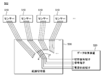
- FIG. 6 is a block diagram illustrating a configuration example of a conventional data collection system 500.
- the data collection system 500 includes a plurality of sensors 510, a data collection device 520, and a wiring switch 530.
- the data collection device 520 supplies power to the connected sensor 510 and inputs data measured by the sensor 510.
- Each sensor 510 and the data collection device 520 are connected via a wiring switch 530.
- the data collection device 520 controls the wiring switch 530 by the switching signal, and sequentially switches the connection destination sensor 510 to collect data.
- the data collection device 520 has a large number of connected sensors 510, but in many cases it is sufficient to acquire data sequentially. For this reason, it is set as the connection form using the wiring switch 530. FIG.
- the conventional data collection device 520 needs to connect the wiring switch 530 and each sensor 510 individually.
- a plurality of wires such as a data signal wire and a power supply wire are used.
- the number of sensors 510 is large, the number of wirings is enormous. For this reason, the mounting of the sensor 510 has been complicated.
- an object of the present invention is to provide a data collection system that can reduce the complexity of wiring even when the number of sensors is large.
- a data collection system of the present invention is a data collection system comprising a plurality of sensor modules having a sensor unit and a data collection device, wherein the data collection device has a clock for each of them.
- a clock output unit that outputs to the sensor module; an enable signal output unit that outputs an enable signal to a predetermined sensor module at intervals equal to or greater than the number of clocks corresponding to the number of sensor modules; a counter that counts the number of clocks;
- a sensor signal input unit that inputs data output from the module via a bus line and records the data in association with a count value, and the sensor module uses the clock as a trigger to send the enable signal to a sensor in the next stage Functions as a shift register to send to the module and enables No.
- the sensor module may include an amplifier that is enabled / disabled by the enable signal.
- the data collection device can supply power through a power supply line connected to each sensor module by a bus.
- the sensor module may include a switch that switches power supply to the sensor unit with the enable signal.
- the data collection device may record a count value corresponding to a sensor module that does not require data input, and shorten the clock interval when counting the count value.
- the counter can reset a count value when the enable signal is output.
- a data collection system that can reduce the complexity of wiring even when the number of sensors is large is provided.
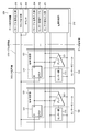
- FIG. 1 is a block diagram illustrating a configuration of a data collection system 10 according to the present embodiment.
- the data collection system 10 includes a plurality of sensor modules 100 and a data collection device 200.
- Each sensor module 100 and the data collection device 200 are connected by a data type signal line and a power supply line in a bus topology. For this reason, since it is not necessary to perform wiring independently for every sensor module 100, even if the number of sensor modules 100 increases, the complexity of wiring can be reduced.
- the switching control line includes a clock signal line and an enable signal line.
- the clock signal lines are connected by a bus topology, and the enable signal lines are connected in a loop shape or cascade (see FIG. 2). For this reason, the sensor module 100 is connected in multiple stages with respect to the enable signal line.
- Each sensor module 100 includes a sensor unit 110 and a signal switching unit 120.
- the sensor unit 110 is supplied with power from the data collection device, measures physical quantities such as temperature, voltage, and magnetism, and outputs them as analog data in a predetermined range.
- the sensor unit 110 of each sensor module 100 only needs to have the same data output interface, and the measurement target of each sensor module 100 does not have to be the same.
- the signal switching unit 120 receives power supply from the data collection device 200 via the power supply line, and outputs data output from the sensor unit 110 to the data collection device 200 via the data signal line.
- the signal switching unit 120 of each sensor module 100 receives the switching control signal from the data collection device 200 via the switching control line and sequentially operates. Thereby, the data collection device 200 can sequentially acquire data from each sensor module 100.
- FIG. 2 is a block diagram illustrating a specific configuration example of the sensor module 100 and the data collection device 200.
- the signal switching unit 120 of the sensor module 100 includes an amplifier 121 with a disable function and a D-type flip-flop 122.
- the data collection device 200 includes a clock output unit 201, an enable signal output unit 202, a counter 203, an enable signal input unit 204, a sensor signal input unit 205, a sensor management table 206, and a power supply unit 210.
- the Q output of the D-type flip-flop 122 is inverted and input to the disable terminal of the amplifier 121 with the disable function, and becomes the D input of the signal switching unit 120 of the next stage through the enable signal line.
- the output signal of the enable signal output unit 202 is input by the enable signal line
- the Q output of the last stage sensor module 100 is input to the enable signal input unit 204 by the enable signal line. Is done.
- the clock from the clock output unit 201 is input to the clock terminal CLK of each D-type flip-flop 122 through the clock signal line. Therefore, the D-type flip-flop 122 of the sensor module 100 connected in multiple stages forms a shift register in which the enable signal output from the enable signal output unit 202 is shifted to the next stage for each clock of the clock output unit 201. It will be. If each sensor module 100 forms a shift register, a circuit other than the D-type flip-flop 122 may be used.
- the amplifier 121 with the disable function outputs high impedance in the disabled state, and amplifies the analog data output from the sensor unit 110 in the enabled state and outputs it to the data signal line. That is, output data of the sensor unit 110 is sent to the data collection device 200 only when an enable signal is sent from the previous stage.
- the sensor module 100 at this time is referred to as an enabled state.
- a normal amplifier and an output switch may be used to switch the output switch on and off by the Q output of the D-type flip-flop 122.
- the clock output unit 201 outputs a clock at a predetermined cycle. It is also possible to output a clock faster than usual or to stop the clock.
- the enable signal output unit 202 outputs an enable signal (H) at intervals equal to or greater than the number of clocks corresponding to the number of stages of the sensor module 100. For this reason, the plurality of sensor modules 100 are not simultaneously enabled.
- Counter 203 counts the number of clocks.
- the counter 203 is reset when the enable signal output unit 202 outputs the enable signal (H). Thereby, the count value of the counter 203 can be associated with the sensor module 100 in the enabled state.
- the enable signal input unit 204 inputs an enable signal output from the last sensor module 100. Thereby, it can be confirmed that the enable signal has shifted to all the sensor modules 100. Further, the number of sensor modules 100 can be confirmed by referring to the count value of the counter 203 when the enable signal input unit 204 inputs the enable signal. However, the enable signal input unit 204 may be omitted.
- the sensor signal input unit 205 inputs data output from the sensor module 100 and performs digital conversion.
- Digital conversion may be performed on the sensor module 100 side.
- the sensor management table 206 records the data input by the sensor signal input unit 205 in association with the count value.
- the attributes of the sensor unit 110 may be recorded.
- a count value corresponding to the sensor module 100 may be recorded. In this case, when the counter 203 counts the count value, the time spent for data collection can be shortened by sending a clock at a high speed.
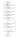
- data collection can be performed according to the procedure shown in FIG. That is, at the timing of data collection, the D-type flip-flop 122 of each sensor module 100 is initialized (S101). Note that the timing of data collection can be continuous, at predetermined intervals, based on user instructions, and the like.
- Initialization of the D-type flip-flop 122 may be performed by outputting more clocks than the number of sensor modules 100 while keeping the output of the enable signal output unit 202 at L. At this time, in order to shorten the processing time, it is preferable to send the clock at a higher speed than usual. Alternatively, a separate reset signal line may be provided to initialize the D-type flip-flops 122 all at once.
- the output of the enable signal output unit 202 is set to H and an enable signal is output (S102).
- the counter 203 is reset.
- the output of the enable signal output unit 202 is H and the clock is output (S103)
- the count value of the counter 203 advances, and the sensor module 100 in the first stage is enabled and outputs data of the sensor unit 110. Therefore, the data input to the sensor signal input unit 205 is recorded in the sensor management table 206 in association with the count value (S104).
- the output of the enable signal output unit 202 is set to L (S105), and a clock is output (S106).
- the count value of the counter 203 advances and the sensor modules 100 are sequentially enabled. Therefore, the data input to the sensor signal input unit 205 is recorded in the sensor management table 206 in association with the count value ( S107).
- the clock cycle can be arbitrarily determined as a cycle suitable for the data collection system 10.
- the process of outputting the clock (S106) and recording the input data (S107) is repeated until the enable signal input unit 204 inputs the enable signal (S108). Note that it may be repeated until the count value of the counter 203 reaches the number of sensor modules 100.
- next data collection process may be performed continuously immediately after the end of the data collection process shown in the figure, or the next data collection process may be performed with a predetermined or unspecified interval. It may be.
- the data collection system 10 since the amplifier 121 with the disable function is in a power saving mode in the disabled state, the data collection system 10 according to the present embodiment supplies power to the sensor module 100 with a bus type connection. An increase in power consumption can be prevented.
- a switch 111 may be provided in the power supply line of the sensor unit 110, and on / off may be switched by an enable signal, similar to the amplifier 121 with the disable function. .
- the sensor unit 110 operates only in the enabled state.
- the sensor signal input unit 205 records output data when the state of the sensor unit 110 is stabilized.
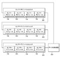
- a plurality of sensor modules 100 are unitized to form a sensor module unit 300, whereby handling of a large number of sensor units 110 can be facilitated.
- the complexity of wiring can be further reduced while the basic configuration remains the same.
- DESCRIPTION OF SYMBOLS 10 ... Data collection system, 100 ... Sensor module, 110 ... Sensor part, 111 ... Switch, 120 ... Signal switching part, 121 ... Amplifier with a disable function, 122 ... D-type flip-flop, 200 ... Data collection device, 201 ... Clock Output unit 202 ... Enable signal output unit 203 ... Counter 204 ... Enable signal input unit 205 ... Sensor signal input unit 206 ... Sensor management table 210 ... Power supply unit 300 ... Sensor module unit
Landscapes
- Physics & Mathematics (AREA)
- General Physics & Mathematics (AREA)
- Engineering & Computer Science (AREA)
- Computer Networks & Wireless Communication (AREA)
- Signal Processing (AREA)
- Arrangements For Transmission Of Measured Signals (AREA)
Abstract
Priority Applications (4)
| Application Number | Priority Date | Filing Date | Title |
|---|---|---|---|
| US15/536,499 US9997059B2 (en) | 2014-12-17 | 2015-11-17 | Data collection system |
| RU2017120987A RU2667031C1 (ru) | 2014-12-17 | 2015-11-17 | Система сбора данных |
| EP15869720.1A EP3236444B1 (fr) | 2014-12-17 | 2015-11-17 | Système de collecte de données |
| CN201580068996.2A CN107111926B (zh) | 2014-12-17 | 2015-11-17 | 数据收集系统 |
Applications Claiming Priority (2)
| Application Number | Priority Date | Filing Date | Title |
|---|---|---|---|
| JP2014-254629 | 2014-12-17 | ||
| JP2014254629A JP6375928B2 (ja) | 2014-12-17 | 2014-12-17 | データ収集システム |
Publications (1)
| Publication Number | Publication Date |
|---|---|
| WO2016098512A1 true WO2016098512A1 (fr) | 2016-06-23 |
Family
ID=56126411
Family Applications (1)
| Application Number | Title | Priority Date | Filing Date |
|---|---|---|---|
| PCT/JP2015/082268 WO2016098512A1 (fr) | 2014-12-17 | 2015-11-17 | Système de collecte de données |
Country Status (6)
| Country | Link |
|---|---|
| US (1) | US9997059B2 (fr) |
| EP (1) | EP3236444B1 (fr) |
| JP (1) | JP6375928B2 (fr) |
| CN (1) | CN107111926B (fr) |
| RU (1) | RU2667031C1 (fr) |
| WO (1) | WO2016098512A1 (fr) |
Families Citing this family (3)
| Publication number | Priority date | Publication date | Assignee | Title |
|---|---|---|---|---|
| US11751768B2 (en) | 2017-12-28 | 2023-09-12 | Techno-Commons, Inc. | Biological data measuring device |
| JP6874748B2 (ja) * | 2018-09-05 | 2021-05-19 | 横河電機株式会社 | 環境情報収集システム及び航空機 |
| DE102019204313A1 (de) * | 2019-03-28 | 2020-10-01 | Siemens Aktiengesellschaft | Elektroenergieübertragungseinrichtung sowie Analyseverfahren |
Citations (4)
| Publication number | Priority date | Publication date | Assignee | Title |
|---|---|---|---|---|
| JPS6335096A (ja) * | 1985-07-26 | 1988-02-15 | ミューテック ミクロテヒニク ウント イーバーヴァッフングスジュステーメ ゲーエムベーハー | 複数個の測定要素を持つ測定装置 |
| JPS6489839A (en) * | 1987-09-30 | 1989-04-05 | Kuroda Precision Ind Ltd | Serial transmission system for parallel sensor signal |
| JPH08298513A (ja) * | 1995-04-26 | 1996-11-12 | Omron Corp | 制御通信システム |
| JP2002271878A (ja) * | 2000-06-30 | 2002-09-20 | Haamorinku:Kk | 制御・監視信号伝送システム |
Family Cites Families (10)
| Publication number | Priority date | Publication date | Assignee | Title |
|---|---|---|---|---|
| DE3623705A1 (de) | 1985-07-26 | 1987-01-29 | Mitec Moderne Ind Gmbh | Adressierbare schaltungsanordnung |
| DE3620595A1 (de) | 1985-07-26 | 1987-02-05 | Mitec Moderne Ind Gmbh | Kabel |
| US5247292A (en) * | 1987-09-30 | 1993-09-21 | Nakamura Kiki Engineering Co. Ltd. | Sensor signal transmission system |
| US5223826A (en) * | 1988-08-26 | 1993-06-29 | Nakamura Kiki Engineering Co., Ltd. | Control/supervisory signal transmission system |
| DE10342625A1 (de) * | 2003-09-15 | 2005-04-14 | Robert Bosch Gmbh | Sensor |
| JP2008175638A (ja) | 2007-01-17 | 2008-07-31 | Toshiba Corp | 構造材の欠陥検出装置及び方法 |
| WO2009128216A1 (fr) * | 2008-04-15 | 2009-10-22 | パナソニック株式会社 | Dispositif de moteur, système d'entraînement de moteur muni de dispositifs de moteur, et dispositif de circuit intégré |
| CN101521952A (zh) * | 2009-04-10 | 2009-09-02 | 华中科技大学 | 一种无线传感器网络接入协议的实现装置 |
| JP5884960B2 (ja) * | 2011-03-18 | 2016-03-15 | セイコーエプソン株式会社 | 位置検出システム |
| US10146723B2 (en) * | 2013-11-21 | 2018-12-04 | Sigsense Technologies, Inc. | Sensor data correlation and analysis platform |
-
2014
- 2014-12-17 JP JP2014254629A patent/JP6375928B2/ja active Active
-
2015
- 2015-11-17 RU RU2017120987A patent/RU2667031C1/ru active
- 2015-11-17 WO PCT/JP2015/082268 patent/WO2016098512A1/fr active Application Filing
- 2015-11-17 EP EP15869720.1A patent/EP3236444B1/fr active Active
- 2015-11-17 US US15/536,499 patent/US9997059B2/en active Active
- 2015-11-17 CN CN201580068996.2A patent/CN107111926B/zh active Active
Patent Citations (4)
| Publication number | Priority date | Publication date | Assignee | Title |
|---|---|---|---|---|
| JPS6335096A (ja) * | 1985-07-26 | 1988-02-15 | ミューテック ミクロテヒニク ウント イーバーヴァッフングスジュステーメ ゲーエムベーハー | 複数個の測定要素を持つ測定装置 |
| JPS6489839A (en) * | 1987-09-30 | 1989-04-05 | Kuroda Precision Ind Ltd | Serial transmission system for parallel sensor signal |
| JPH08298513A (ja) * | 1995-04-26 | 1996-11-12 | Omron Corp | 制御通信システム |
| JP2002271878A (ja) * | 2000-06-30 | 2002-09-20 | Haamorinku:Kk | 制御・監視信号伝送システム |
Also Published As
| Publication number | Publication date |
|---|---|
| EP3236444A1 (fr) | 2017-10-25 |
| CN107111926B (zh) | 2020-11-13 |
| RU2667031C1 (ru) | 2018-09-13 |
| JP2016115219A (ja) | 2016-06-23 |
| US20170372598A1 (en) | 2017-12-28 |
| US9997059B2 (en) | 2018-06-12 |
| CN107111926A (zh) | 2017-08-29 |
| EP3236444B1 (fr) | 2020-09-16 |
| EP3236444A4 (fr) | 2018-08-08 |
| JP6375928B2 (ja) | 2018-08-22 |
Similar Documents
| Publication | Publication Date | Title |
|---|---|---|
| TWI465036B (zh) | 多階取樣保持電路 | |
| WO2016098512A1 (fr) | Système de collecte de données | |
| US20170261379A1 (en) | Digital Temperature Sensor With Integrated Timer And Burst Mode | |
| CN201233288Y (zh) | 一种多路数据采集系统 | |
| CN103308850A (zh) | 触控ic模拟前端自测的内建架构及测试方法 | |
| US8358229B2 (en) | Method for use in a sigma-delta analog to digital converter, sigma-delta analog to digital converters and systems comprising a sigma-delta analog to digital converter | |
| US8289336B2 (en) | System and method for processing and representing a sampled signal | |
| CN201159740Y (zh) | 一种多道同时测量装置 | |
| US9152269B2 (en) | Sensing circuit | |
| KR101752580B1 (ko) | 메모리 디바이스에 대한 전력 관리 | |
| EP2965055B1 (fr) | Architecture de capteur à sortie analogique à fil unique | |
| JP2009175053A (ja) | 被測定信号の変化点を検出する装置、方法および試験装置 | |
| JP5494965B2 (ja) | 信号処理装置 | |
| CN101498738B (zh) | 一种多道同时测量装置及测量方法 | |
| US9917684B1 (en) | System and method for sampled analog clock distribution | |
| CN107516123A (zh) | 高灵敏性的计数器过电压动作计数系统 | |
| RU2554508C2 (ru) | Устройство ввода аналоговых сигналов | |
| RU2208800C2 (ru) | Устройство для измерения электрической мощности и энергии | |
| CN116481599A (zh) | 多通道信号采集设备和传感器系统 | |
| JP2017011667A (ja) | センサ装置及びセンシング方法 | |
| KR101734006B1 (ko) | 전력 소모를 감소시키는 데이터 판독 회로 | |
| JP2003008437A (ja) | 多入力a/d変換装置 | |
| CN105094034A (zh) | 多路数据采集系统 | |
| RU59915U1 (ru) | Аналого-цифровой преобразователь | |
| US8629695B2 (en) | Multi-stage sample and hold circuit |
Legal Events
| Date | Code | Title | Description |
|---|---|---|---|
| 121 | Ep: the epo has been informed by wipo that ep was designated in this application |
Ref document number: 15869720 Country of ref document: EP Kind code of ref document: A1 |
|
| REEP | Request for entry into the european phase |
Ref document number: 2015869720 Country of ref document: EP |
|
| WWE | Wipo information: entry into national phase |
Ref document number: 15536499 Country of ref document: US |
|
| NENP | Non-entry into the national phase |
Ref country code: DE |
|
| ENP | Entry into the national phase |
Ref document number: 2017120987 Country of ref document: RU Kind code of ref document: A |