WO2016093261A1 - 接続体の検査方法、接続体、導電性粒子及び異方性導電接着剤 - Google Patents
接続体の検査方法、接続体、導電性粒子及び異方性導電接着剤 Download PDFInfo
- Publication number
- WO2016093261A1 WO2016093261A1 PCT/JP2015/084478 JP2015084478W WO2016093261A1 WO 2016093261 A1 WO2016093261 A1 WO 2016093261A1 JP 2015084478 W JP2015084478 W JP 2015084478W WO 2016093261 A1 WO2016093261 A1 WO 2016093261A1
- Authority
- WO
- WIPO (PCT)
- Prior art keywords
- resin core
- resin
- conductive
- conductive particles
- connection terminal
- Prior art date
Links
Images


Classifications
-
- C—CHEMISTRY; METALLURGY
- C09—DYES; PAINTS; POLISHES; NATURAL RESINS; ADHESIVES; COMPOSITIONS NOT OTHERWISE PROVIDED FOR; APPLICATIONS OF MATERIALS NOT OTHERWISE PROVIDED FOR
- C09J—ADHESIVES; NON-MECHANICAL ASPECTS OF ADHESIVE PROCESSES IN GENERAL; ADHESIVE PROCESSES NOT PROVIDED FOR ELSEWHERE; USE OF MATERIALS AS ADHESIVES
- C09J9/00—Adhesives characterised by their physical nature or the effects produced, e.g. glue sticks
- C09J9/02—Electrically-conducting adhesives
-
- G—PHYSICS
- G01—MEASURING; TESTING
- G01N—INVESTIGATING OR ANALYSING MATERIALS BY DETERMINING THEIR CHEMICAL OR PHYSICAL PROPERTIES
- G01N21/00—Investigating or analysing materials by the use of optical means, i.e. using sub-millimetre waves, infrared, visible or ultraviolet light
- G01N21/84—Systems specially adapted for particular applications
- G01N21/88—Investigating the presence of flaws or contamination
- G01N21/8803—Visual inspection
-
- C—CHEMISTRY; METALLURGY
- C09—DYES; PAINTS; POLISHES; NATURAL RESINS; ADHESIVES; COMPOSITIONS NOT OTHERWISE PROVIDED FOR; APPLICATIONS OF MATERIALS NOT OTHERWISE PROVIDED FOR
- C09J—ADHESIVES; NON-MECHANICAL ASPECTS OF ADHESIVE PROCESSES IN GENERAL; ADHESIVE PROCESSES NOT PROVIDED FOR ELSEWHERE; USE OF MATERIALS AS ADHESIVES
- C09J11/00—Features of adhesives not provided for in group C09J9/00, e.g. additives
- C09J11/02—Non-macromolecular additives
-
- C—CHEMISTRY; METALLURGY
- C09—DYES; PAINTS; POLISHES; NATURAL RESINS; ADHESIVES; COMPOSITIONS NOT OTHERWISE PROVIDED FOR; APPLICATIONS OF MATERIALS NOT OTHERWISE PROVIDED FOR
- C09J—ADHESIVES; NON-MECHANICAL ASPECTS OF ADHESIVE PROCESSES IN GENERAL; ADHESIVE PROCESSES NOT PROVIDED FOR ELSEWHERE; USE OF MATERIALS AS ADHESIVES
- C09J201/00—Adhesives based on unspecified macromolecular compounds
-
- H—ELECTRICITY
- H01—ELECTRIC ELEMENTS
- H01B—CABLES; CONDUCTORS; INSULATORS; SELECTION OF MATERIALS FOR THEIR CONDUCTIVE, INSULATING OR DIELECTRIC PROPERTIES
- H01B1/00—Conductors or conductive bodies characterised by the conductive materials; Selection of materials as conductors
-
- H—ELECTRICITY
- H01—ELECTRIC ELEMENTS
- H01B—CABLES; CONDUCTORS; INSULATORS; SELECTION OF MATERIALS FOR THEIR CONDUCTIVE, INSULATING OR DIELECTRIC PROPERTIES
- H01B1/00—Conductors or conductive bodies characterised by the conductive materials; Selection of materials as conductors
- H01B1/20—Conductive material dispersed in non-conductive organic material
- H01B1/22—Conductive material dispersed in non-conductive organic material the conductive material comprising metals or alloys
-
- H—ELECTRICITY
- H01—ELECTRIC ELEMENTS
- H01B—CABLES; CONDUCTORS; INSULATORS; SELECTION OF MATERIALS FOR THEIR CONDUCTIVE, INSULATING OR DIELECTRIC PROPERTIES
- H01B5/00—Non-insulated conductors or conductive bodies characterised by their form
-
- H—ELECTRICITY
- H01—ELECTRIC ELEMENTS
- H01B—CABLES; CONDUCTORS; INSULATORS; SELECTION OF MATERIALS FOR THEIR CONDUCTIVE, INSULATING OR DIELECTRIC PROPERTIES
- H01B5/00—Non-insulated conductors or conductive bodies characterised by their form
- H01B5/16—Non-insulated conductors or conductive bodies characterised by their form comprising conductive material in insulating or poorly conductive material, e.g. conductive rubber
-
- H—ELECTRICITY
- H01—ELECTRIC ELEMENTS
- H01R—ELECTRICALLY-CONDUCTIVE CONNECTIONS; STRUCTURAL ASSOCIATIONS OF A PLURALITY OF MUTUALLY-INSULATED ELECTRICAL CONNECTING ELEMENTS; COUPLING DEVICES; CURRENT COLLECTORS
- H01R11/00—Individual connecting elements providing two or more spaced connecting locations for conductive members which are, or may be, thereby interconnected, e.g. end pieces for wires or cables supported by the wire or cable and having means for facilitating electrical connection to some other wire, terminal, or conductive member, blocks of binding posts
- H01R11/01—Individual connecting elements providing two or more spaced connecting locations for conductive members which are, or may be, thereby interconnected, e.g. end pieces for wires or cables supported by the wire or cable and having means for facilitating electrical connection to some other wire, terminal, or conductive member, blocks of binding posts characterised by the form or arrangement of the conductive interconnection between the connecting locations
-
- H—ELECTRICITY
- H01—ELECTRIC ELEMENTS
- H01R—ELECTRICALLY-CONDUCTIVE CONNECTIONS; STRUCTURAL ASSOCIATIONS OF A PLURALITY OF MUTUALLY-INSULATED ELECTRICAL CONNECTING ELEMENTS; COUPLING DEVICES; CURRENT COLLECTORS
- H01R43/00—Apparatus or processes specially adapted for manufacturing, assembling, maintaining, or repairing of line connectors or current collectors or for joining electric conductors
-
- H—ELECTRICITY
- H05—ELECTRIC TECHNIQUES NOT OTHERWISE PROVIDED FOR
- H05K—PRINTED CIRCUITS; CASINGS OR CONSTRUCTIONAL DETAILS OF ELECTRIC APPARATUS; MANUFACTURE OF ASSEMBLAGES OF ELECTRICAL COMPONENTS
- H05K3/00—Apparatus or processes for manufacturing printed circuits
- H05K3/30—Assembling printed circuits with electric components, e.g. with resistor
- H05K3/32—Assembling printed circuits with electric components, e.g. with resistor electrically connecting electric components or wires to printed circuits
- H05K3/34—Assembling printed circuits with electric components, e.g. with resistor electrically connecting electric components or wires to printed circuits by soldering
-
- G—PHYSICS
- G01—MEASURING; TESTING
- G01N—INVESTIGATING OR ANALYSING MATERIALS BY DETERMINING THEIR CHEMICAL OR PHYSICAL PROPERTIES
- G01N21/00—Investigating or analysing materials by the use of optical means, i.e. using sub-millimetre waves, infrared, visible or ultraviolet light
- G01N21/84—Systems specially adapted for particular applications
- G01N21/88—Investigating the presence of flaws or contamination
- G01N21/95—Investigating the presence of flaws or contamination characterised by the material or shape of the object to be examined
- G01N2021/9513—Liquid crystal panels
Definitions
- the present invention relates to a method for inspecting a connection body in which a transparent electrode formed on a transparent substrate and a connection terminal of an electronic component are anisotropically conductively connected, and the connection body, in particular, captured between the transparent electrode and the connection terminal.
- the present invention relates to a connection body inspection method with improved visibility of conductive particles, a connection body, conductive particles, and an anisotropic conductive adhesive.
- liquid crystal display devices and organic EL panels have been used as various display means such as televisions, PC monitors, mobile phones, smart phones, portable game machines, tablet terminals, wearable terminals, and in-vehicle monitors.
- the driving IC is directly mounted on the glass substrate of the display panel using an anisotropic conductive film (ACF).
- ACF anisotropic conductive film
- a plurality of transparent electrodes made of ITO (indium tin oxide) or the like are formed on a glass substrate on which an IC or a flexible substrate is mounted, and an electronic component such as an IC or a flexible substrate is connected to the transparent electrode.
- the electronic component connected to the glass substrate has a plurality of electrode terminals formed on the mounting surface corresponding to the transparent electrodes, and is thermocompression-bonded on the glass substrate through the anisotropic conductive film, thereby A transparent electrode is connected.
- An anisotropic conductive film is a film in which conductive particles are mixed in a binder resin, and heat conduction is performed between two conductors to provide electrical continuity between the conductors with the conductive particles. Resin maintains the mechanical connection between the conductors.
- a highly reliable thermosetting binder resin is usually used, but a photocurable binder resin or a photothermal binder resin may be used.
- the anisotropic conductive film When connecting an electronic component to a transparent electrode via such an anisotropic conductive film, first, the anisotropic conductive film is temporarily pasted onto the transparent electrode of the glass substrate by a temporary pressure bonding means. Subsequently, after mounting the electronic component on the glass substrate via the anisotropic conductive film to form a temporary connection body, the electronic component is moved to the transparent electrode side together with the anisotropic conductive film by a thermocompression bonding means such as a thermocompression bonding head. Heat and press. By the heating by the thermocompression bonding head, the anisotropic conductive film undergoes a thermosetting reaction, whereby the electronic component is bonded onto the transparent electrode.
- a thermocompression bonding means such as a thermocompression bonding head.
- the conductive layer is generally formed by plating the surface of the resin core with a conductive material such as nickel or gold. The formed one is used.
- the conductive particles sandwiched between the transparent electrode and the connection terminal make conduction between the transparent electrode and the connection terminal through the conductive layer.
- the conductive layer may be peeled off from the surface of the resin core due to friction with the transparent electrode or the connection terminal due to accidental vibration during pressure bonding during anisotropic connection.
- the conductive layer may be eluted from the conductive particles by an acid or the like generated in the binder resin at the time of anisotropic connection or before and after the treatment. As described above, when the conductive particles are sandwiched between the transparent electrode and the connection terminal in a state where the surface of the resin core is exposed, the conductivity may be impaired.
- Such a phenomenon may occur for all conductive particles trapped between a set of transparent electrodes and connection terminals, or a plurality of conductive particles trapped between a set of transparent electrodes and connection terminals. May occur in some of the sex particles.
- connection bodies in which glass substrates and electronic components such as ICs and flexible substrates are anisotropically connected there are several possible causes for the decrease in electrical conductivity. Due to the finer pitch of the wiring, it takes a considerable amount of man-hours and time to specify the wiring. That is, whether the cause of the conduction failure is due to the constituent member side of the connection body such as a glass substrate or an electronic component, or due to peeling or elution of the conductive layer of the conductive particles described above, the thermocompression bonding step In order to improve the yield, it is strongly required to identify the factors such as the inadequate indentation of the conductive particles due to the alignment, thermocompression tool setting and accuracy, etc. ing.
- the resin core of the conductive particles is observed to be colorless or translucent, and if the conductive layer peels off and elutes, it is difficult to grasp the position of the conductive particles captured on the connection terminals and the degree of collapse. It is.
- connection body inspection method a connection body, conductive particles, and an anisotropic conductive adhesive that can easily and quickly perform inspection of conductive particles after manufacturing the connection body.
- a connection body inspection method is a connection body in which a transparent electrode formed on a transparent substrate and a connection terminal of an electronic component are connected by an anisotropic conductive adhesive.
- the conductive particles sandwiched between the transparent electrode and the connection terminal are such that the resin core is covered with a conductive layer, and the resin core is colored in a color different from the connection terminal, It is detected by coloring the resin core that it is captured on the transparent electrode and the surface of the resin core is exposed.
- connection body is a connection body in which a transparent electrode formed on a transparent substrate and a connection terminal of an electronic component are connected by an anisotropic conductive adhesive, and the connection between the transparent electrode and the connection terminal.
- the conductive particles sandwiched between the resin particles are coated with a conductive layer, and the resin particles are colored in a color different from the connection terminals, and the conductive particles captured on the transparent electrode are In addition, the fact that the surface of the resin core is exposed is made visible by coloring the resin core.
- the conductive particles according to the present invention are the conductive particles contained in the adhesive that anisotropically conductively connects the transparent electrodes formed on the transparent substrate and the connection terminals of the electronic component.
- a conductive layer covering the surface of the core, the resin core is colored in a color different from the connection terminal, and the surface of the resin core is exposed by the coloring of the resin core. is there.
- the anisotropic conductive adhesive according to the present invention is an anisotropic conductive adhesive that contains conductive particles in a binder resin and connects a transparent electrode formed on a transparent substrate and a connection terminal of an electronic component.
- the conductive particles have a resin core and a conductive layer covering the surface of the resin core, the resin core is colored in a color different from the connection terminal, and the surface of the resin core is exposed. It is made visible by coloring the resin core.
- the conductive particles sandwiched between the transparent electrode and the connection terminal are such that the resin core is covered with the conductive layer, and at least a part of the resin core is colored in a color different from that of the connection terminal. Therefore, when the colored surface of the resin core is exposed, the conductive particles captured by the connection terminals after crimping can improve the visibility, and the degree of peeling and elution of the conductive layer and the conductivity can be improved. It is possible to easily grasp the crushing state of the sex particles.
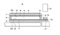
- FIG. 1 is a cross-sectional view of a liquid crystal display panel shown as an example of a connection body.
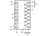
- FIG. 2 is a plan view showing a mounting portion of the transparent substrate.
- FIG. 3 is a cross-sectional view showing a connection process between the liquid crystal driving IC and the transparent substrate.
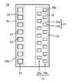
- FIG. 4 is a plan view showing a mounting surface of the liquid crystal driving IC.
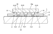
- FIG. 5 is a cross-sectional view showing an anisotropic conductive film.
- FIG. 6 is a cross-sectional view showing conductive particles.
- FIG. 1 is a cross-sectional view of a liquid crystal display panel shown as an example of a connection body.
- FIG. 2 is a plan view showing a mounting portion of the transparent substrate.
- FIG. 3 is a cross-sectional view showing a connection process between the liquid crystal driving IC and the transparent substrate.
- FIG. 4 is a plan view showing a mounting surface of the liquid crystal driving IC.
- FIG. 5 is a cross
- FIG. 7 is a bottom view showing the conductive particles captured by the bumps from the back side of the transparent substrate of the connection body, (A) is the conductive particles in which peeling / elution of the conductive layer does not occur, and (B) is Conductive particles with peeling / elution of the conductive layer laminated on the colored resin core, (C) shows conductive particles with peeling / elution of the conductive layer laminated on the uncolored resin core .
- connection body inspection method a connection body inspection method, a connection body, conductive particles, and an anisotropic conductive adhesive to which the present invention is applied will be described in detail with reference to the drawings.
- the present invention is not limited to the following embodiments, and various modifications can be made without departing from the scope of the present invention.
- the drawings are schematic, and the ratio of each dimension may be different from the actual one. Specific dimensions should be determined in consideration of the following description. Moreover, it is a matter of course that portions having different dimensional relationships and ratios are included between the drawings.
- the liquid crystal display panel 10 includes two transparent substrates 11 and 12 made of a glass substrate and the like, and the transparent substrates 11 and 12 are bonded to each other by a frame-shaped seal 13. .
- the liquid crystal 14 is sealed in a space surrounded by the transparent substrates 11 and 12 to form a panel display unit 15.
- the transparent substrates 11 and 12 have a pair of striped transparent electrodes 16 and 17 made of ITO (Indium Tin Oxide) or the like on both inner surfaces facing each other so as to intersect each other.
- the transparent electrodes 16 and 17 are configured such that a pixel as a minimum unit of liquid crystal display is configured by the intersection of the transparent electrodes 16 and 17.
- one transparent substrate 12 is formed to have a larger planar dimension than the other transparent substrate 11, and an edge 12a of the formed transparent substrate 12 has an electronic component.
- a mounting portion 27 on which the liquid crystal driving IC 18 is mounted is provided. 2 and 3, the mounting unit 27 includes an input terminal row 20 in which a plurality of input terminals 19 of the transparent electrode 17 are arranged, and an output terminal row 22 in which a plurality of output terminals 21 are arranged,
- a substrate-side alignment mark 31 is formed so as to overlap the IC-side alignment mark 32 provided on the liquid crystal driving IC 18.
- the mounting unit 27 includes, for example, a first terminal region 27a in which one input terminal row 20 is formed, and two output terminal rows 22a and 22b arranged in parallel in the width direction orthogonal to the arrangement direction of the output terminals 21. And a second terminal region 27b.
- the output terminal 21 and the output terminal row 22 include a first output terminal row 22a in which the first output terminals 21a are arranged on the inner side, that is, the input terminal row 20 side, and a second output on the outer side, that is, the outer edge side of the mounting portion 27. And a second output terminal row 22b in which the terminals 21b are arranged.
- the liquid crystal driving IC 18 can selectively apply a liquid crystal driving voltage to the pixels to change the alignment of the liquid crystal partially to perform a predetermined liquid crystal display.
- the liquid crystal driving IC 18 has an input in which a plurality of input bumps 23 electrically connected to the input terminal 19 of the transparent electrode 17 are arranged on the mounting surface 18 a on the transparent substrate 12.
- An output bump row 26 in which a plurality of output bumps 25 that are electrically connected to the bump row 24 and the output terminal 21 of the transparent electrode 17 are arranged is formed.
- the first bump region 18b in which the input bumps 23 are arranged in a line along one side edge of the mounting surface 18a and the width direction orthogonal to the arrangement direction of the output bumps 25 are arranged in parallel.
- the output bump 25 and the output bump row 26 include a first output bump row 26a in which the first output bumps 25a are arranged on the inner side, that is, the input bump row 24 side, and a second output on the outer side, that is, the outer edge side of the mounting surface 18a.
- the first and second output bumps 25a and 25b are arranged in a staggered manner in a plurality of rows along the other side edge facing the one side edge.
- the input / output bumps 23 and 25 and the input / output terminals 19 and 21 provided on the mounting portion 27 of the transparent substrate 12 are formed with the same number and the same pitch, respectively, so that the transparent substrate 12 and the liquid crystal driving IC 18 are aligned. Connected by being connected.
- one or a plurality of input bump rows 24 are provided on one side edge of the mounting surface 18a. Any configuration in which the output bump rows 26 are arranged in one or a plurality of rows on the other side edge may be employed.
- a part of the input / output bumps 23 and 25 arranged in a line may be a plurality of lines, and a part of the input / output bumps 23 and 25 arranged in a line may be a line. Good.
- the input / output bump rows 24 and 26 may be formed in a straight array in which the arrays of the plurality of input / output bumps 23 and 25 are parallel and adjacent bumps are arranged in parallel.
- 23 and 25 may be formed in a staggered arrangement in which adjacent bumps are evenly displaced from each other in parallel.
- the input / output bumps 23 and 25 may be arranged along the long side of the IC substrate, and the side bumps may be formed along the short side of the IC substrate.
- the input / output bumps 23 and 25 may be formed with the same dimensions or different dimensions.
- the input / output bump rows 24 and 26 the input / output bumps 23 and 25 formed with the same dimensions may be arranged symmetrically or asymmetrically.
- the input / output bumps 23 and 25 formed with different dimensions may be arranged asymmetrically. May be.
- liquid crystal driving IC 18 With recent miniaturization and higher functionality of liquid crystal display devices and other electronic devices, electronic components such as the liquid crystal driving IC 18 are required to be smaller and lower in height, and the input / output bumps 23 and 25 are also high in height. Is low (for example, 6 to 15 ⁇ m).
- the liquid crystal driving IC 18 is formed with an IC side alignment mark 32 for alignment with the transparent substrate 12 by being superimposed on the mounting surface 18a with the substrate side alignment mark 31. Since the wiring pitch of the transparent electrodes 17 of the transparent substrate 12 and the fine pitches of the input / output bumps 23 and 25 of the liquid crystal driving IC 18 are increasing, the liquid crystal driving IC 18 and the transparent substrate 12 are aligned with high precision. Adjustment is required.
- the substrate side alignment mark 31 and the IC side alignment mark 32 various marks that can be aligned with the transparent substrate 12 and the liquid crystal driving IC 18 can be used.
- the liquid crystal driving IC 18 is connected to the input / output terminals 19 and 21 of the transparent electrode 17 formed in the mounting portion 27 using the anisotropic conductive film 1 as an adhesive for circuit connection.
- the anisotropic conductive film 1 contains conductive particles 4, and input / output bumps 23 and 25 of the liquid crystal driving IC 18 and input / output terminals 19 of the transparent electrode 17 formed on the mounting portion 27 of the transparent substrate 12. 21 is electrically connected through the conductive particles 4.
- the anisotropic conductive film 1 is thermocompression bonded by the thermocompression bonding head 33 to fluidize the binder resin, so that the conductive particles 4 are connected to the input / output terminals 19 and 21 and the input / output bumps 23 and 25 of the liquid crystal driving IC 18.
- the binder resin is cured in this state. Thereby, the anisotropic conductive film 1 electrically and mechanically connects the transparent substrate 12 and the liquid crystal driving IC 18.
- an alignment film 28 subjected to a predetermined rubbing process is formed on both the transparent electrodes 16 and 17, and the initial alignment of liquid crystal molecules is regulated by the alignment film 28.
- a pair of polarizing plates 29a and 29b are disposed outside the transparent substrates 11 and 12, and the light transmitted from a light source (not shown) such as a backlight is transmitted by these polarizing plates 29a and 29b. The vibration direction is regulated.
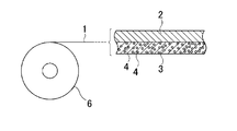
- an anisotropic conductive film (ACF) 1 usually has a binder resin layer (adhesive layer) 3 containing conductive particles 4 on a release film 2 as a base material. It is formed.
- the anisotropic conductive film 1 is a thermosetting adhesive or a photo-curing adhesive such as ultraviolet rays, and is attached to the mounting portion 27 where the input / output terminals 19 and 21 of the transparent substrate 12 of the liquid crystal display panel 10 are formed.
- the liquid crystal driving IC 18 is mounted and fluidized by being thermally pressed by the thermocompression bonding head 33, and the conductive particles 4 are opposed to the input / output terminals 19 and 21 of the transparent electrode 17 and the liquid crystal driving IC 18 inserted.
- the conductive particles 4 are crushed between the output bumps 23 and 25 and hardened in a state of being crushed by heating or ultraviolet irradiation.
- the anisotropic conductive film 1 can connect the transparent substrate 12 and the liquid crystal driving IC 18 to make them conductive.
- conductive particles 4 are blended in a normal binder resin layer 3 containing a film-forming resin, a thermosetting resin, a latent curing agent, a silane coupling agent, and the like.
- the release film 2 that supports the binder resin layer 3 includes, for example, a release agent such as silicone on PET (PolyEthylene Terephthalate), OPP (Oriented Polypropylene), PMP (Poly-4-methylpentene-1), PTFE (Polytetrafluoroethylene), and the like. It coats and prevents the anisotropic conductive film 1 from drying, and maintains the shape of the anisotropic conductive film 1.
- a release agent such as silicone on PET (PolyEthylene Terephthalate), OPP (Oriented Polypropylene), PMP (Poly-4-methylpentene-1), PTFE (Polytetrafluoroethylene), and the like. It coats and prevents the anisotropic conductive film 1 from drying, and maintains the shape of the anisotropic conductive film 1.
- the film-forming resin contained in the binder resin layer 3 is preferably a resin having an average molecular weight of about 10,000 to 80,000.
- the film forming resin include various resins such as an epoxy resin, a modified epoxy resin, a urethane resin, and a phenoxy resin. Among these, phenoxy resin is particularly preferable from the viewpoint of film formation state, connection reliability, and the like.
- thermosetting resin is not particularly limited, and examples thereof include commercially available epoxy resins and acrylic resins.
- the epoxy resin is not particularly limited.
- naphthalene type epoxy resin biphenyl type epoxy resin, phenol novolac type epoxy resin, bisphenol type epoxy resin, stilbene type epoxy resin, triphenolmethane type epoxy resin, phenol aralkyl type epoxy resin.
- an acrylic compound, liquid acrylate, etc. can be selected suitably.
- what made acrylate the methacrylate can also be selected from methyl acrylate, ethyl acrylate, isopropy
- the latent curing agent is not particularly limited, and examples thereof include various curing agents such as a heat curing type and a UV curing type.
- the latent curing agent does not normally react, but is activated by various triggers selected according to applications such as heat, light, and pressure, and starts the reaction.
- the activation method of the thermal activation type latent curing agent includes a method of generating active species (cation, anion, radical) by a dissociation reaction by heating, etc., and it is stably dispersed in the epoxy resin near room temperature, and epoxy at high temperature
- active species cation, anion, radical
- Thermally active latent curing agents include imidazole, hydrazide, boron trifluoride-amine complexes, sulfonium salts, amine imides, polyamine salts, dicyandiamide, etc., and modified products thereof. The above mixture may be sufficient. Among these, a microcapsule type imidazole-based latent curing agent is preferable.
- the silane coupling agent is not particularly limited, and examples thereof include an epoxy type, an amino type, a mercapto sulfide type, and a ureido type. By adding the silane coupling agent, the adhesion at the interface between the organic material and the inorganic material is improved.
- the conductive particle 4 has a resin core 4a and a conductive layer 4b covering the resin core 4a, and the resin core 4a is different from the input bump 23 and the output bump 25 of the liquid crystal driving IC 18. Colored.
- the resin core 4a particles made of a plastic material excellent in compressive deformation are preferably used.
- (meth) acrylate resin polystyrene resin, styrene- (meth) acrylic copolymer resin, urethane resin, epoxy resin , Phenol resin, acrylonitrile / styrene (AS) resin, benzoguanamine resin, divinylbenzene resin, styrene resin, polyester resin, and the like.
- the resin core 4a is formed of a (meth) acrylate resin
- the (meth) acrylic resin has a (meth) acrylate ester and, if necessary, a reactive double bond copolymerizable therewith. It is preferable that it is a copolymer with the compound which has and a bifunctional or polyfunctional monomer.
- the polystyrene resin is composed of a styrene derivative, a compound having a reactive double bond that can be copolymerized therewith, and a bifunctional or polyfunctional compound, if necessary. It is preferably a copolymer with a functional monomer.
- the (meth) acrylic resin is preferably a (co) polymer of a (meth) acrylic acid ester. Copolymers of (meth) acrylic acid ester monomers and other monomers can also be used.
- (meth) acrylic acid ester monomers examples include methyl (meth) acrylate, ethyl (meth) acrylate, propyl (meth) acrylate, butyl (meth) acrylate, 2-ethylhexyl (meth) acrylate, and lauryl.
- the resin core 4a forming the conductive particles of the present invention is a polystyrene resin
- specific examples of the styrene monomer include styrene, methyl styrene, dimethyl styrene, trimethyl styrene, ethyl styrene, diethyl styrene, Alkyl styrenes such as triethyl styrene, propyl styrene, butyl styrene, hexyl styrene, hebutyl styrene and octyl styrene; halogenated styrenes such as fluorostyrene, chlorostyrene, bromostyrene, dibromostyrene, iodostyrene and chloromethylstyrene; and nitro Mention may be made of styrene, acetyl
- the resin core 4a is preferably formed of any one of the above (meth) acrylic resins or styrene resins, but may be formed of a composition made of these resins. Further, it may be a copolymer of the (meth) acrylic acid ester monomer and the styrene monomer.
- the (meth) acrylic resin or styrene resin includes a (meth) acrylic acid ester monomer and / or a styrene monomer as described above and, if necessary, another monomer that can be copolymerized. It may be polymerized.
- Examples of the above-mentioned (meth) acrylic acid ester monomers or other monomers copolymerizable with styrene monomers include vinyl monomers and unsaturated carboxylic acid monomers.
- the resin core 4a is comprised with the polymer of the acrylic monomer, for example, may comprise it with the polymer of the monomer containing a urethane compound and an acrylate ester. it can.
- the acrylic monomer refers to both an acrylic ester (acrylate) and a methacrylic ester (methacrylate).
- the monomer includes an oligomer that is a polymer of two or more monomers as long as it is polymerized by heating, ultraviolet irradiation, or the like.
- the acrylic resin constituting the resin core 4a of the present invention is composed of a polymer of a monomer containing a urethane compound and an acrylate ester
- the urethane compound contains 5 parts by weight or more with respect to 100 parts by weight of the monomer. It is preferable that the content is 25 parts by weight or more.
- polyfunctional urethane acrylate can be used, for example, bifunctional urethane acrylate can be used.
- the resin core 4a is colored at least partly or entirely in a different color from the input bumps 23 and the output bumps 25 of the liquid crystal driving IC 18 by a colorant. Thereby, the resin core 4a can improve visibility, when the surface of the resin core 4a is exposed by peeling or eluting the conductive layer 4b.
- the resin core 4a when the resin core 4a is made of an acrylic resin, the resin core 4a can be colored by adding a filler serving as a colorant to polymerize the acrylic monomer, and the resin core 4a can be made of a polystyrene resin. When forming, it can carry out by adding the filler used as a coloring agent and polymerizing a styrene-type monomer.
- the resin core 4a is colored in a complementary color (opposite color) to the colors of the input / output bumps 23 and 25, thereby improving visibility.
- a complementary color (opposite color) refers to a color on the opposite side of the hue circle. Specifically, when the target color is placed at the center of one region obtained by equally dividing the hue circle into four, the complementary color (opposite color) is a color belonging to a region not adjacent to the region to which the target color belongs. It shall be said.
- the resin core 4a is preferably colored with a black filler when the surfaces of the input / output bumps 23 and 25 are covered with a white conductive layer.
- the resin core 4a may be colored with a white filler when the surfaces of the input / output bumps 23 and 25 are covered with a conductive layer having a yellow metallic luster such as gold.
- the resin core 4a when the resin core 4a is coated with a material having a metallic luster such as gold, silver or copper as a conductive material constituting the surfaces of the input / output bumps 23 and 25, the resin core 4a is colored with a white filler such as titanium oxide. It is preferable. Further, when the resin core 4a is covered with a white material such as zinc as a conductive material constituting the surfaces of the input / output bumps 23 and 25, the resin core 4a is colored with a black filler such as titanium black, carbon black, or iron oxide. It is preferred that
- the coloring agent which colors the resin core 4a has insulation.
- the colorant is preferably a substance having an insulation resistance measured at 25 ° C. and 70% RH of 1 ⁇ 10 8 ⁇ / cm or more.
- the insulation resistance can be measured by, for example, a general insulation resistance meter.
- the colorant for coloring the resin core 4a may be a conductive material.
- the conduction resistance value between the input / output bumps 23 and 25 and the input / output terminals 19 and 21 connected via the conductive particles 4 can be easily reduced.
- the size of the filler coloring the resin core 4a is preferably less than 30% of the particle diameter of the conductive particles 4, more preferably 20% or less, and even more preferably 10% or less.
- the size of the filler coloring the resin core 4a is 30% or more of the particle diameter of the conductive particles 4, the elasticity of the conductive particles 4 decreases, and input / output immediately after anisotropic connection or after a reliability test. This is because the variation in the gap between the bumps 23 and 25 and the input / output terminals 19 and 21 cannot be followed and the conduction resistance value may increase.
- the filler coloring the resin core 4a is preferably spherical. This is because, as will be described later, when the connection body is inspected, the degree of crushing and the like can be easily compared.
- the size of the filler coloring the resin core 4a is uniform. Specifically, it is preferable that 90% of the total number of fillers used be within a size that is within ⁇ 20% of the average diameter of the fillers. Thereby, in the test
- the blending amount of the filler coloring the resin core 4a is preferably 30 vol% or less. If the blending amount of the filler is more than 30 vol%, the elasticity of the conductive particles 4 is impaired, and the connection reliability may be lowered. Moreover, it is preferable that the compounding quantity of a filler shall be 2 vol% or more. When the filler content is less than 2 vol%, the visibility of the resin core 4a cannot be improved.
- the conductive layer 4b formed on the surface of the resin core 4a is composed of conductive metals generally used as conductive layers of conductive particles, alloys containing these metals, conductive properties Metal oxides or other conductive materials can be used to form.
- the conductive layer 4b is formed of Ni, Ni alloy, Au, or the like.
- the conductive layer 4b is formed by a physical method such as vapor deposition, ion sputtering, electroless plating, or thermal spraying, a chemical method for chemically bonding a conductive material to the resin core surface having a functional group, or surface activity. It can be formed by a method of adsorbing a conductive material on the surface of the resin core using an agent or the like. Such a conductive layer 4b does not need to be a single layer, and a plurality of layers may be laminated.
- the thickness of the conductive layer 4b is usually in the range of 0.01 to 10.0 ⁇ m, preferably 0.05 to 5 ⁇ m, and more preferably 0.2 to 2 ⁇ m.
- An insulating layer made of an insulating resin may be further formed on the surface of the conductive layer 4b.
- a method for forming an insulating layer for example, a method for forming a discontinuous insulating layer made of polyvinylidene fluoride by a hybridization system is shown. Treat with vinylidene at a temperature of 85-115 ° C. for 5-10 minutes.
- the thickness of this insulating layer is usually about 0.1 to 0.5 ⁇ m.
- this insulating layer may coat
- the conductive particles 4 of the present invention are used for an anisotropic conductive adhesive (anisotropic conductive film) as will be described later, the conductive particles 4 are usually 1 to 50 ⁇ m, preferably 3 to 10 ⁇ m average particles. It is good to have a diameter.
- the shape of the anisotropic conductive film 1 is not particularly limited.
- the anisotropic conductive film 1 has a long tape shape that can be wound around a take-up reel 6 and is cut and used for a predetermined length. can do.
- the adhesive according to the present invention is not limited to this, and for example, an insulating adhesive layer made of only the binder resin 3 and a conductive particle-containing layer made of the binder resin 3 containing the conductive particles 4 are laminated. Can do. Moreover, in this invention, you may use the anisotropic conductive paste which consists of a binder resin composition which mix
- FIG. The anisotropic conductive adhesive according to the present invention includes both the anisotropic conductive film 1 and the anisotropic conductive paste.
- the input / output bumps 23 and 25 for capturing the conductive particles 4 are formed of a conductive metal, an alloy containing these metals, a conductive ceramic, a conductive metal oxide, or other conductive material. .
- Examples of conductive metals include Zn, Al, Sb, U, Cd, Ga, Ca, Au, Ag, Co, Sn, Se, Fe, Cu, Th, Pb, Ni, Pd, Be, and Mg. Can do. Moreover, the said metal may be used independently, 2 or more types may be used, and another element, a compound (for example, solder) etc. may be added.
- Examples of conductive ceramics include Vo 2 , Ru 2 O, SiC, ZrO 2 , Ta 2 N, ZrN, NbN, VN, TiB 2 , ZrB, HfB 2 , TaB 2 , MoB 2 , CrB 2 , B 4 C , MoB, ZrC, VC and TiC.
- examples of the conductive material other than the above include carbon particles such as carbon and graphite, and ITO.
- the input / output bumps 23 and 25 contain gold.
- the electrical resistance value is lowered, the spreadability is improved, and good conductivity can be obtained.
- an anisotropic conductive adhesive an anisotropic conductive film, anisotropic conductive paste
- the input / output terminals 19, 21 is less likely to be damaged when conductively connected to 21.
- the input / output bumps 23 and 25 it is preferable to use, for example, a nickel (Ni) metal layer having a gold (Au) layer formed thereon (substitute with gold (Au)).
- connection process Next, a connection process for connecting the liquid crystal driving IC 18 to the transparent substrate 12 will be described. First, the anisotropic conductive film 1 is temporarily attached on the mounting portion 27 where the input / output terminals 19 and 21 of the transparent substrate 12 are formed. Next, the transparent substrate 12 is placed on the stage of the connection device, and the liquid crystal driving IC 18 is disposed on the mounting portion 27 of the transparent substrate 12 via the anisotropic conductive film 1.
- thermocompression bonding head 33 heated to a predetermined temperature for curing the binder resin layer 3 is hot-pressed from above the liquid crystal driving IC 18 at a predetermined pressure and time.
- the binder resin layer 3 of the anisotropic conductive film 1 exhibits fluidity and flows out from between the mounting surface 18a of the liquid crystal driving IC 18 and the mounting portion 27 of the transparent substrate 12, and the conductive in the binder resin layer 3
- the conductive particles 4 are sandwiched between the input / output bumps 23 and 25 of the liquid crystal driving IC 18 and the input / output terminals 19 and 21 of the transparent substrate 12 and are crushed.
- the conductive particles 4 are electrically connected between the input / output bumps 23 and 25 and the input / output terminals 19 and 21, and the binder resin heated by the thermocompression bonding head 33 in this state is cured. To do.
- the liquid crystal display panel 10 in which electrical conductivity is ensured between the input / output bumps 23 and 25 of the liquid crystal driving IC 18 and the input / output terminals 19 and 21 formed on the transparent substrate 12 can be manufactured.
- the conductive particles 4 sandwiched between the input / output bumps 23, 25 and the input / output terminals 19, 21 have the input / output bumps 23, 25 as a background. Observation from the back surface of the transparent substrate 12 becomes possible.
- the conductive particles 4 that are not between the input / output bumps 23 and 25 and the input / output terminals 19 and 21 are dispersed in the binder resin in the space 35 between the adjacent input / output bumps 23 and 25, and are electrically insulated. The state is maintained. Therefore, the liquid crystal display panel 10 is electrically connected only between the input / output bumps 23 and 25 of the liquid crystal driving IC 18 and the input / output terminals 19 and 21 of the transparent substrate 12.
- the anisotropic conductive film 1 is not limited to the thermosetting type, and may be a photo-curing type or a photo-heat combined type adhesive as long as pressure connection is performed.
- the conductive particles 4 sandwiched between the input / output bumps 23 and 25 and the input / output terminals 19 and 21 can be observed from the back surface of the transparent substrate 12 for visual inspection. Attached. As shown in FIG. 7A, the conductive particles 4 in which no peeling or elution occurs in the conductive layer 4b can be visually recognized with the input / output bumps 23 and 25 as a background, and the number of particles captured, the degree of collapse, etc. Can be easily identified.
- the conductive particles 4 are electrically conductive from the surface of the resin core 4a due to friction with the input / output terminals 19 and 21 and the input / output bumps 23 and 25 due to the occurrence of accidental vibration during pressure bonding during anisotropic connection.
- the layer 4b may be peeled off, or the conductive layer 4b may be eluted by an acid or the like generated in the binder resin at the time of anisotropic connection or before and after the treatment, and the surface of the resin core 4a may be exposed.
- Such a phenomenon may occur with respect to all the conductive particles 4 captured between the set of input / output terminals 19 and 21 and the input / output bumps 23 and 25, or the set of input / output terminals 19 and 21. May occur in some of the plurality of conductive particles 4 captured between the input / output bumps 23 and 25. Moreover, peeling and elution of the conductive layer 4b occur over the entire surface of the resin core 4a, and the entire surface of the resin core 4a is exposed.
- the resin core 4a is colored in a color different from that of the input / output bumps 23 and 25, the visibility of the conductive particles 4 from which the conductive layer 4b is peeled off or eluted is enhanced. As shown in FIG. 5, even with the input / output bumps 23 and 25 in the background, it is possible to quickly inspect the presence / absence and number of the conductive particles 4 in which the conductive layer 4b is peeled off or eluted, the degree of collapse, and the like.
- the resin core 4c in the case of the resin core 4c that is not colored at all, the resin core 4c is generally transparent even if the conductive layer 4b is peeled off or eluted and the resin core is exposed. Since it is translucent, it is difficult to determine the presence or absence and number of conductive particles in which the conductive layer 4b is peeled off or eluted with the input / output bumps 23 and 25 in the background.
- the conductive particles 4 to which the present invention is applied have the visibility when the conductive layer 4b is peeled off or eluted because the resin core 4a is colored in a different color from the input / output bumps 23 and 25. It is raised (FIG. 7B).
- the resin core 4a is colored with a white filler when the surfaces of the input / output bumps 23 and 25 are covered with a conductive material having a yellow metallic luster such as gold.
- a white conductive material it is preferable to be colored with a black filler in order to improve visibility.
- the resin core 4a is preferably colored with a white filler such as titanium oxide.
- the resin core 4a is preferably colored with a black filler such as titanium black, carbon black, or iron oxide.
- an anisotropic conductive film using conductive particles in which a conductive layer is formed on a colored resin core and an anisotropic conductive film using conductive particles in which the resin core is not colored
- the binder resin layer of the anisotropic conductive film used for connecting the IC for evaluation was 60 parts by mass of phenoxy resin (trade name: YP50, manufactured by Nippon Steel Chemical Co., Ltd.), epoxy resin (trade name: jER828, manufactured by Mitsubishi Chemical Corporation).
- a binder resin composition prepared by adding 40 parts by mass and 2 parts by mass of a cationic curing agent (trade name: SI-60L, manufactured by Sanshin Chemical Industry Co., Ltd.) to a solvent is prepared, and this binder resin composition is applied onto a release film. Formed by drying.
- the conductive particles contained in the binder resin layer of the anisotropic conductive film have a conductive layer formed on a colored resin core.
- the resin cores were prepared in proportions of 60 parts by weight and 40 parts by weight, respectively, using A-HD-N manufactured by Shin-Nakamura Chemical Co., Ltd. as the acrylic monomer and U-6LPA manufactured by Shin-Nakamura Chemical Co., Ltd. as the urethane acrylate. Titanium oxide (Taibak R-820, manufactured by Ishihara Sangyo Co., Ltd., filler system: 0.26 ⁇ m) as a colorant was dispersed in the acrylic monomer and urethane acrylate, and acrylic resin particles were prepared by emulsion polymerization.
- the acrylic resin particles were coated with nickel by a sputtering method to obtain conductive particles having a particle diameter of 3.2 ⁇ m.
- the thickness of the nickel layer is 0.15 ⁇ m.
- an evaluation IC was prepared in which a plurality of bumps (Au-plated) having an outer shape of 1.8 mm ⁇ 20 mm, a thickness of 0.5 mm, a width of 30 ⁇ m, a length of 85 ⁇ m, and a height of 15 ⁇ m were arranged.
- the bump surface of the evaluation IC has a metallic luster.
- An anisotropic conductive film was temporarily attached to the glass substrate for evaluation, an evaluation IC was mounted, and a connector sample was prepared by thermocompression bonding with a thermocompression bonding head under the conditions of 170 ° C., 60 MPa, and 5 seconds.
- a connector sample was prepared by thermocompression bonding with a thermocompression bonding head under the conditions of 170 ° C., 60 MPa, and 5 seconds.
- the initial stage conduction resistance and the conduction resistance after a reliability test were measured.
- the connected body sample was placed in a thermostatic chamber having a temperature of 85 ° C. and a humidity of 85% RH for 500 hours.
- the initial conduction resistance was OK for less than 10 ⁇ and NG for 10 ⁇ or more. Further, the conduction resistance after the reliability test is preferably less than 20 ⁇ , more preferably less than 10 ⁇ , even more preferably less than 5 ⁇ , and 20 ⁇ or more is defective.
- connection body sample the electroconductive particle captured by bump of IC for evaluation was observed using the optical microscope from the back surface of the glass substrate for evaluation, and the visibility of the electroconductive particle from which the electroconductive layer peeled was evaluated. .
- connection conditions are the same (170 ° C., 60 MPa, 5 sec).
- the number of conductive particles captured on the bumps of the IC for evaluation is counted in advance, and the ratio of the conductive particles with the resin core surface exposed at a magnification of 50 times using an optical microscope is visible.
- the ratio is 90% or more, ⁇ (best), and when the ratio of the conductive particles whose resin core surface is exposed at a magnification of 50 times is 50% or more and less than 90% is marked as ⁇ (good), the magnification is 50 times.
- the case where the ratio of the conductive particles whose resin core surface was exposed was 10% or more and less than 50% was ⁇ (normal), and the ratio of the conductive particles whose resin core surface was exposed at a magnification of 50 was 10
- the case of less than% was defined as x (defect).
- Example 1 In Example 1, 2 vol% of titanium oxide (Taibak R-820, manufactured by Ishihara Sangyo Co., Ltd.) was dispersed in the urethane compound as a colorant, and acrylic resin particles were prepared by emulsion polymerization.
- the connected body sample according to Example 1 has an initial conduction resistance of 1.2 ⁇ , a conduction resistance after reliability test of 2.5 ⁇ , and the visibility of the conductive particles from which the conductive layer has peeled is ⁇ (normal). It was.
- Example 2 In Example 2, 8 vol% of titanium oxide (Taibak R-820, manufactured by Ishihara Sangyo Co., Ltd.) was dispersed as a colorant in the urethane compound, and acrylic resin particles were prepared by emulsion polymerization.
- the connected body sample according to Example 2 had an initial conduction resistance of 1.7 ⁇ , a conduction resistance after reliability test of 3.3 ⁇ , and the visibility of the conductive particles from which the conductive layer was peeled off was good (good). It was.
- Example 3 In Example 3, 15 vol% of titanium oxide (Taibak R-820, manufactured by Ishihara Sangyo Co., Ltd.) was dispersed in the urethane compound as a colorant, and acrylic resin particles were prepared by emulsion polymerization.
- the connected body sample according to Example 3 had an initial conduction resistance of 2.2 ⁇ , a conduction resistance after the reliability test of 4.8 ⁇ , and the visibility of the conductive particles from which the conductive layer was peeled off was good (good). It was.
- Example 4 In Example 4, 23 vol% of titanium oxide (Taibak R-820, manufactured by Ishihara Sangyo Co., Ltd.) was dispersed as a colorant in the urethane compound, and acrylic resin particles were prepared by emulsion polymerization.
- the connected body sample according to Example 4 had an initial conduction resistance of 3.2 ⁇ , a conduction resistance after a reliability test of 9.3 ⁇ , and the visibility of the conductive particles from which the conductive layer was peeled off was good (good). It was.
- Example 5 In Example 5, 30 vol% of titanium oxide (Taibak R-820, manufactured by Ishihara Sangyo Co., Ltd.) was dispersed in the urethane compound as a colorant, and acrylic resin particles were prepared by emulsion polymerization.
- the connected body sample according to Example 5 had an initial conduction resistance of 4.3 ⁇ , a conduction resistance after a reliability test of 17.5 ⁇ , and the visibility of the conductive particles from which the conductive layer was peeled off was good (good). It was.
- Comparative Example 1 acrylic resin particles were prepared without adding a colorant to the urethane compound.
- the connection body sample according to Comparative Example 1 has an initial conduction resistance of 1.2 ⁇ , a conduction resistance after a reliability test of 2.1 ⁇ , and the visibility of the conductive particles from which the conductive layer has peeled is x (defective). It was.
- Comparative Example 2 In Comparative Example 2, 1 vol% of titanium oxide (Taibak R-820 manufactured by Ishihara Sangyo Co., Ltd.) was dispersed as a colorant in the urethane compound, and acrylic resin particles were prepared by emulsion polymerization.
- the connected body sample according to Comparative Example 2 has an initial conduction resistance of 1.1 ⁇ , a conduction resistance after a reliability test of 2.2 ⁇ , and the visibility of the conductive particles from which the conductive layer has peeled is x (defective). It was.
- Comparative Example 3 In Comparative Example 3, 38 vol% of titanium oxide (Taibak R-820, manufactured by Ishihara Sangyo Co., Ltd.) was dispersed as a colorant in the urethane compound, and acrylic resin particles were prepared by emulsion polymerization.
- the connected body sample according to Comparative Example 3 had an initial conduction resistance of 6.9 ⁇ , a conduction resistance after a reliability test of 21.9 ⁇ , and the visibility of the conductive particles from which the conductive layer was peeled off was good (good). It was.
- Examples 1-5 the visibility of the conductive particles was high, and the evaluation was ⁇ (ordinary) or higher. This is because the connected body samples according to Examples 1 to 5 are formed using a conductive adhesive film in which an appropriate amount of a colorant is added and colored conductive particles are blended. This is because it was possible to secure the sex.
- Comparative Example 1 since the resin core of the conductive particles is not colored, and in Comparative Example 2, the addition amount of the colorant is small. In any case, the conductive particles with the conductive layer peeled off against the background of the IC bumps are visible. The inspection process was complicated.
- Comparative Example 3 since the amount of the colorant added was too large, the resin core became hard, and the followability with respect to the expansion and contraction of the distance between the IC bump and the ITO film was deteriorated. It became lacking in nature.
- thermocompression bonding head 1 anisotropic conductive film, 2 release film, 3 binder resin layer, 4 conductive particles, 4a resin core, 4b conductive layer, 6 take-up reel, 10 liquid crystal display panel, 11, 12 transparent substrate, 12a edge, 13 Seal, 14 liquid crystal, 15 panel display, 16, 17 transparent electrode, 18 liquid crystal drive IC, 18a mounting surface, 19 input terminal, 20 input terminal row, 21 output terminal, 22 output terminal row, 23 input bump, 25 output Bump, 24 input bump row, 26 output bump row, 27 mounting part, 33 thermocompression bonding head
Landscapes
- Chemical & Material Sciences (AREA)
- Engineering & Computer Science (AREA)
- Manufacturing & Machinery (AREA)
- Organic Chemistry (AREA)
- Physics & Mathematics (AREA)
- Microelectronics & Electronic Packaging (AREA)
- Dispersion Chemistry (AREA)
- Spectroscopy & Molecular Physics (AREA)
- Analytical Chemistry (AREA)
- Pathology (AREA)
- Health & Medical Sciences (AREA)
- Biochemistry (AREA)
- General Health & Medical Sciences (AREA)
- General Physics & Mathematics (AREA)
- Immunology (AREA)
- Life Sciences & Earth Sciences (AREA)
- Wire Bonding (AREA)
- Adhesives Or Adhesive Processes (AREA)
- Non-Insulated Conductors (AREA)
- Manufacturing Of Electrical Connectors (AREA)
- Electric Connection Of Electric Components To Printed Circuits (AREA)
- Conductive Materials (AREA)
- Liquid Crystal (AREA)
Abstract
接続体の製造後における導電性粒子の検査を簡易、迅速に行うことができる接続体の検査方法、接続体、導電性粒子及び異方性導電接着剤を提供する。 透明基板(12)に形成された透明電極(19,21)と電子部品(18)の接続端子(23,25)とが異方性導電接着剤(1)によって接続されている接続体の検査方法において、透明電極(19,21)と接続端子(23,25)との間に挟持される導電性粒子(4)は、樹脂コア(4a)が導電層(4b)によって被覆されてなり、かつ、樹脂コア4aが接続端子(23,25)と異なる色に着色され、透明電極(19,21)上に捕捉され、樹脂コア(4a)の表面が露出したことを上記樹脂コアの着色によって検出する。
Description
本発明は、透明基板に形成された透明電極と電子部品の接続端子とが異方性導電接続された接続体の検査方法及び接続体に関し、特に透明電極と接続端子との間に捕捉された導電性粒子の視認性が向上された接続体の検査方法、接続体、導電性粒子及び異方性導電接着剤に関する。
本出願は、日本国において2014年12月10日に出願された日本特許出願番号特願2014-250384を基礎として優先権を主張するものであり、この出願は参照されることにより、本出願に援用される。
本出願は、日本国において2014年12月10日に出願された日本特許出願番号特願2014-250384を基礎として優先権を主張するものであり、この出願は参照されることにより、本出願に援用される。
従来から、テレビやPCモニタ、携帯電話やスマートホン、携帯型ゲーム機、タブレット端末やウェアラブル端末、あるいは車載用モニタ等の各種表示手段として、液晶表示装置や有機ELパネルが用いられている。近年、このような表示装置においては、ファインピッチ化、軽量薄型化等の観点から、異方性導電フィルム(ACF:Anisotropic Conductive Film)を用いて、駆動用ICを直接表示パネルのガラス基板上に実装する工法や、駆動回路等が形成されたフレキシブル基板を直接ガラス基板に実装する工法が採用されている。
ICやフレキシブル基板が実装されるガラス基板には、ITO(酸化インジウムスズ)等からなる透明電極が複数形成され、この透明電極上にICやフレキシブル基板等の電子部品が接続される。ガラス基板に接続される電子部品は、実装面に、透明電極に対応して複数の電極端子が形成され、異方性導電フィルムを介してガラス基板上に熱圧着されることにより、電極端子と透明電極とが接続される。
異方性導電フィルムは、バインダー樹脂に導電性粒子を混ぜ込んでフィルム状としたもので、2つの導体間で加熱圧着されることにより導電性粒子で導体間の電気的導通がとられ、バインダー樹脂にて導体間の機械的接続が保持される。異方性導電フィルムを構成する接着剤としては、通常、信頼性の高い熱硬化性のバインダー樹脂が用いられるが、光硬化性のバインダー樹脂又は光熱併用型のバインダー樹脂であってもよい。
このような異方性導電フィルムを介して電子部品を透明電極へ接続する場合は、先ず、ガラス基板の透明電極上に異方性導電フィルムを仮圧着手段によって仮貼りする。続いて、異方性導電フィルムを介してガラス基板上に電子部品を搭載し仮接続体を形成した後、熱圧着ヘッド等の熱圧着手段によって電子部品を異方性導電フィルムとともに透明電極側へ加熱押圧する。この熱圧着ヘッドによる加熱によって、異方性導電フィルムは熱硬化反応を起こし、これにより電子部品が透明電極上に接着される。
ガラス基板の透明電極とICチップ等の電子部品の接続端子との間に挟持される導電性粒子としては、一般に樹脂コアの表面にニッケルや金等の導電材料がメッキされることにより導電層が形成されたものが用いられている。透明電極と接続端子との間に挟持された導電性粒子は、導電層を介して透明電極と接続端子との導通を図る。
ところで、導電性粒子は、異方性接続時における圧着の際に不慮の振動が生じることによる透明電極や接続端子との摩擦によって樹脂コアの表面から導電層が剥離することがある。また、導電性粒子は、異方性接続時あるいはその前後の処理の際にバインダー樹脂に発生した酸等によって導電層が溶出されることがある。このように、導電性粒子が樹脂コアの表面を露出させた状態で透明電極と接続端子との間に挟持されると、導通性が損なわれる恐れがある。
このような現象は、一組の透明電極と接続端子との間に捕捉された全導電性粒子について生じることもあれば、一組の透明電極と接続端子との間に捕捉された複数の導電性粒子の内のいくつかで生じることもある。
ガラス基板とICやフレキシブル基板等の電子部品とが異方性接続された接続体において、導通性の低下要因は複数考えられるが、電子機器の小型化等に伴う基板や電子部品の薄型化、配線のファインピッチ化等によって、その特定にも相当の工数、時間を要する。すなわち、導通不良の要因が、ガラス基板や電子部品等の接続体の構成部材側に起因するものなのか、上述した導電性粒子の導電層の剥離や溶出に起因するものなのか、熱圧着工程におけるアライメント、熱圧着ツールの設定や精度等に起因して導電性粒子の押し込み不足が生じたためなのか、といった要因を早期に洗い出し、改善策を講じることが、歩留りを向上させる上で強く求められている。
そのため、上述した導電性粒子に導電層の剥離や溶出が起こっているか、透明電極と接続端子との間に十分に押し込まれているか、といった判定を容易に行うことができれば、検査工程の負担を減らすことができる。
しかし、導電性粒子の樹脂コアは無色あるいは半透明に観察されるものであり、導電層が剥離、溶出すると、接続端子上に捕捉された導電性粒子の位置や潰れ具合を把握することは困難である。
そこで、本発明は、接続体の製造後における導電性粒子の検査を簡易、迅速に行うことができる接続体の検査方法、接続体、導電性粒子及び異方性導電接着剤を提供することを目的とする。
上述した課題を解決するために、本発明に係る接続体の検査方法は、透明基板に形成された透明電極と電子部品の接続端子とが異方性導電接着剤によって接続されている接続体の検査方法において、上記透明電極と上記接続端子との間に挟持される導電性粒子は、樹脂コアが導電層によって被覆されてなり、かつ、上記樹脂コアが上記接続端子と異なる色に着色され、上記透明電極上に捕捉され、上記樹脂コアの表面が露出したことを上記樹脂コアの着色によって検出するものである。
また、本発明に係る接続体は、透明基板に形成された透明電極と電子部品の接続端子とが異方性導電接着剤によって接続されている接続体において、上記透明電極と上記接続端子との間に挟持される導電性粒子は、樹脂コアが導電層によって被覆されてなり、かつ、上記樹脂コアが上記接続端子と異なる色に着色され、上記透明電極上に捕捉された上記導電性粒子は、上記樹脂コアの表面が露出したことを上記樹脂コアの着色によって視認可能とされるものである。
また、本発明に係る導電性粒子は、透明基板に形成された透明電極と電子部品の接続端子とを異方性導電接続する接着剤に含有される導電性粒子において、樹脂コアと、上記樹脂コアの表面を被覆する導電層とを有し、上記樹脂コアは上記接続端子と異なる色に着色され、上記樹脂コアの表面が露出したことを上記樹脂コアの着色によって視認可能とされるものである。
また、本発明に係る異方性導電接着剤は、バインダー樹脂中に導電性粒子が含有され、透明基板に形成された透明電極と電子部品の接続端子とを接続する異方性導電接着剤において、上記導電性粒子は、樹脂コアと、上記樹脂コアの表面を被覆する導電層とを有し、上記樹脂コアは上記接続端子と異なる色に着色され、上記樹脂コアの表面が露出したことを上記樹脂コアの着色によって視認可能とされるものである。
本発明によれば、透明電極と接続端子との間に挟持される導電性粒子は、樹脂コアが導電層によって被覆され、かつ、樹脂コアの少なくとも一部が接続端子と異なる色に着色されているため、圧着後の接続端子に捕捉されている導電性粒子は、樹脂コアの着色された表面が露出されると、視認性を向上することができ、導電層の剥離や溶出の程度や導電性粒子の潰れ具合を容易に把握できる。
以下、本発明が適用された接続体の検査方法、接続体、導電性粒子及び異方性導電接着剤について、図面を参照しながら詳細に説明する。なお、本発明は、以下の実施形態のみに限定されるものではなく、本発明の要旨を逸脱しない範囲内において種々の変更が可能であることは勿論である。また、図面は模式的なものであり、各寸法の比率等は現実のものとは異なることがある。具体的な寸法等は以下の説明を参酌して判断すべきものである。また、図面相互間においても互いの寸法の関係や比率が異なる部分が含まれていることは勿論である。
[液晶表示パネル]
以下では、本発明が適用された接続体として、ガラス基板に、電子部品として液晶駆動用のICチップが実装された液晶表示パネルを例に説明する。この液晶表示パネル10は、図1に示すように、ガラス基板等からなる二枚の透明基板11,12が対向配置され、これら透明基板11,12が枠状のシール13によって互いに貼り合わされている。そして、液晶表示パネル10は、透明基板11,12によって囲繞された空間内に液晶14が封入されることによりパネル表示部15が形成されている。
以下では、本発明が適用された接続体として、ガラス基板に、電子部品として液晶駆動用のICチップが実装された液晶表示パネルを例に説明する。この液晶表示パネル10は、図1に示すように、ガラス基板等からなる二枚の透明基板11,12が対向配置され、これら透明基板11,12が枠状のシール13によって互いに貼り合わされている。そして、液晶表示パネル10は、透明基板11,12によって囲繞された空間内に液晶14が封入されることによりパネル表示部15が形成されている。
透明基板11,12は、互いに対向する両内側表面に、ITO(酸化インジウムスズ)等からなる縞状の一対の透明電極16,17が、互いに交差するように形成されている。そして、両透明電極16,17は、これら両透明電極16,17の当該交差部位によって液晶表示の最小単位としての画素が構成されるようになっている。
両透明基板11,12のうち、一方の透明基板12は、他方の透明基板11よりも平面寸法が大きく形成されており、この大きく形成された透明基板12の縁部12aには、電子部品として液晶駆動用IC18が実装される実装部27が設けられている。なお、実装部27には、図2、図3に示すように、透明電極17の複数の入力端子19が配列された入力端子列20及び複数の出力端子21が配列された出力端子列22、液晶駆動用IC18に設けられたIC側アライメントマーク32と重畳させる基板側アライメントマーク31が形成されている。
実装部27は、例えば、一つの入力端子列20が形成された第1の端子領域27aと、出力端子21の配列方向と直交する幅方向に並列する2つの出力端子列22a,22bが形成された第2の端子領域27bとを有する。出力端子21及び出力端子列22は、内側すなわち入力端子列20側に第1の出力端子21aが配列された第1の出力端子列22aと、外側すなわち実装部27の外縁側に第2の出力端子21bが配列された第2の出力端子列22bとを有する。
液晶駆動用IC18は、画素に対して液晶駆動電圧を選択的に印加することにより、液晶の配向を部分的に変化させて所定の液晶表示を行うことができるようになっている。また、図3、図4に示すように、液晶駆動用IC18は、透明基板12への実装面18aに、透明電極17の入力端子19と導通接続される複数の入力バンプ23が配列された入力バンプ列24と、透明電極17の出力端子21と導通接続される複数の出力バンプ25が配列された出力バンプ列26が形成されている。
液晶駆動用IC18は、例えば、入力バンプ23が実装面18aの一方の側縁に沿って一列で配列された第1のバンプ領域18bと、出力バンプ25の配列方向と直交する幅方向に並列する2つの出力バンプ列26a,26bが形成された第2のバンプ領域18cとを有する。出力バンプ25及び出力バンプ列26は、内側すなわち入力バンプ列24側に第1の出力バンプ25aが配列された第1の出力バンプ列26aと、外側すなわち実装面18aの外縁側に第2の出力バンプ25bが配列された第2の出力バンプ列26bとを有する。
第1、第2の出力バンプ25a,25bは、一方の側縁と対向する他方の側縁に沿って複数列で千鳥状に配列されている。入出力バンプ23,25と、透明基板12の実装部27に設けられている入出力端子19,21とは、それぞれ同数かつ同ピッチで形成され、透明基板12と液晶駆動用IC18とが位置合わせされて接続されることにより、接続される。
なお、第1、第2のバンプ領域18b,18cにおける入出力バンプ列24,26の配列は、図4に示す以外にも、実装面18aの一方の側縁に入力バンプ列24が一又は複数列で配列され、他方の側縁に出力バンプ列26が一又は複数列で配列されるいずれの構成であってもよい。また、入出力バンプ列24,26は、一列配列の入出力バンプ23,25の一部が複数列となってもよく、複数配列の入出力バンプ23,25の一部が一列となってもよい。さらに、入出力バンプ列24,26は、複数列の各入出力バンプ23,25の配列が平行且つ隣接するバンプ同士が並列するストレート配列で形成されてもよく、あるいは複数列の各入出力バンプ23,25の配列が平行且つ隣接するバンプ同士が均等にズレる千鳥配列で形成されてもよい。
また、液晶駆動用IC18は、IC基板の長辺に沿って入出力バンプ23,25を配列させるとともに、IC基板の短辺に沿ってサイドバンプを形成してもよい。なお、入出力バンプ23,25は、同一寸法で形成してもよく、異なる寸法で形成してもよい。また、入出力バンプ列24,26は、同一寸法で形成された入出力バンプ23,25が対称又は非対称に配列されてもよく、異なる寸法で形成された入出力バンプ23,25が非対称に配列されてもよい。
なお、近年の液晶表示装置その他の電子機器の小型化、高機能化に伴い、液晶駆動用IC18等の電子部品も小型化、低背化が求められ、入出力バンプ23,25もその高さが低くなっている(例えば6~15μm)。
また、液晶駆動用IC18は、実装面18aに、基板側アライメントマーク31と重畳させることにより、透明基板12に対するアライメントを行うIC側アライメントマーク32が形成されている。なお、透明基板12の透明電極17の配線ピッチや液晶駆動用IC18の入出力バンプ23,25のファインピッチ化が進んでいることから、液晶駆動用IC18と透明基板12とは、高精度のアライメント調整が求められている。
基板側アライメントマーク31及びIC側アライメントマーク32は、組み合わされることにより透明基板12と液晶駆動用IC18とのアライメントが取れる種々のマークを用いることができる。
実装部27に形成されている透明電極17の入出力端子19,21上には、回路接続用接着剤として異方性導電フィルム1を用いて液晶駆動用IC18が接続される。異方性導電フィルム1は、導電性粒子4を含有しており、液晶駆動用IC18の入出力バンプ23,25と透明基板12の実装部27に形成された透明電極17の入出力端子19,21とを、導電性粒子4を介して電気的に接続させるものである。この異方性導電フィルム1は、熱圧着ヘッド33によって熱圧着されることによりバインダー樹脂が流動化して導電性粒子4が入出力端子19,21と液晶駆動用IC18の入出力バンプ23,25との間で押し潰され、この状態でバインダー樹脂が硬化する。これにより、異方性導電フィルム1は、透明基板12と液晶駆動用IC18とを電気的、機械的に接続する。
また、両透明電極16,17上には、所定のラビング処理が施された配向膜28が形成されており、この配向膜28によって液晶分子の初期配向が規制されるようになっている。さらに、両透明基板11,12の外側には、一対の偏光板29a,29bが配設されており、これら両偏光板29a,29bによってバックライト等の光源(図示せず)からの透過光の振動方向が規制されるようになっている。
[異方性導電フィルム]
次いで、異方性導電フィルム1について説明する。異方性導電フィルム(ACF:Anisotropic Conductive Film)1は、図5に示すように、通常、基材となる剥離フィルム2上に導電性粒子4を含有するバインダー樹脂層(接着剤層)3が形成されたものである。異方性導電フィルム1は、熱硬化型あるいは紫外線等の光硬化型の接着剤であり、液晶表示パネル10の透明基板12の入出力端子19,21が形成された実装部27に貼着されるとともに液晶駆動用IC18が搭載され、熱圧着ヘッド33により熱加圧されることにより流動化して導電性粒子4が相対向する透明電極17の入出力端子19,21と液晶駆動用IC18の入出力バンプ23,25との間で押し潰され、加熱あるいは紫外線照射により、導電性粒子4が押し潰された状態で硬化する。これにより、異方性導電フィルム1は、透明基板12と液晶駆動用IC18とを接続し、導通させることができる。
次いで、異方性導電フィルム1について説明する。異方性導電フィルム(ACF:Anisotropic Conductive Film)1は、図5に示すように、通常、基材となる剥離フィルム2上に導電性粒子4を含有するバインダー樹脂層(接着剤層)3が形成されたものである。異方性導電フィルム1は、熱硬化型あるいは紫外線等の光硬化型の接着剤であり、液晶表示パネル10の透明基板12の入出力端子19,21が形成された実装部27に貼着されるとともに液晶駆動用IC18が搭載され、熱圧着ヘッド33により熱加圧されることにより流動化して導電性粒子4が相対向する透明電極17の入出力端子19,21と液晶駆動用IC18の入出力バンプ23,25との間で押し潰され、加熱あるいは紫外線照射により、導電性粒子4が押し潰された状態で硬化する。これにより、異方性導電フィルム1は、透明基板12と液晶駆動用IC18とを接続し、導通させることができる。
また、異方性導電フィルム1は、膜形成樹脂、熱硬化性樹脂、潜在性硬化剤、シランカップリング剤等を含有する通常のバインダー樹脂層3に導電性粒子4が配合されている。
バインダー樹脂層3を支持する剥離フィルム2は、例えば、PET(Poly Ethylene Terephthalate)、OPP(Oriented Polypropylene)、PMP(Poly-4-methylpentene-1)、PTFE(Polytetrafluoroethylene)等にシリコーン等の剥離剤を塗布してなり、異方性導電フィルム1の乾燥を防ぐとともに、異方性導電フィルム1の形状を維持する。
バインダー樹脂層3に含有される膜形成樹脂としては、平均分子量が10000~80000程度の樹脂が好ましい。膜形成樹脂としては、エポキシ樹脂、変形エポキシ樹脂、ウレタン樹脂、フェノキシ樹脂等の各種の樹脂が挙げられる。中でも、膜形成状態、接続信頼性等の観点からフェノキシ樹脂が特に好ましい。
熱硬化性樹脂としては、特に限定されず、例えば、市販のエポキシ樹脂、アクリル樹脂等が挙げられる。
エポキシ樹脂としては、特に限定されないが、例えば、ナフタレン型エポキシ樹脂、ビフェニル型エポキシ樹脂、フェノールノボラック型エポキシ樹脂、ビスフェノール型エポキシ樹脂、スチルベン型エポキシ樹脂、トリフェノールメタン型エポキシ樹脂、フェノールアラルキル型エポキシ樹脂、ナフトール型エポキシ樹脂、ジシクロペンタジエン型エポキシ樹脂、トリフェニルメタン型エポキシ樹脂等が挙げられる。これらは単独でも、2種以上の組み合わせであってもよい。
アクリル樹脂としては、特に制限はなく、目的に応じてアクリル化合物、液状アクリレート等を適宜選択することができる。例えば、メチルアクリレート、エチルアクリレート、イソプロピルアクリレート、イソブチルアクリレート、エポキシアクリレート、エチレングリコールジアクリレート、ジエチレングリコールジアクリレート、トリメチロールプロパントリアクリレート、ジメチロールトリシクロデカンジアクリレート、テトラメチレングリコールテトラアクリレート、2-ヒドロキシ-1,3-ジアクリロキシプロパン、2,2-ビス[4-(アクリロキシメトキシ)フェニル]プロパン、2,2-ビス[4-(アクリロキシエトキシ)フェニル]プロパン、ジシクロペンテニルアクリレート、トリシクロデカニルアクリレート、トリス(アクリロキシエチル)イソシアヌレート、ウレタンアクリレート、エポキシアクリレート等を挙げることができる。なお、アクリレートをメタクリレートにしたものを用いることもできる。これらは、1種単独で使用してもよいし、2種以上を併用してもよい。
潜在性硬化剤としては、特に限定されないが、例えば、加熱硬化型、UV硬化型等の各種硬化剤が挙げられる。潜在性硬化剤は、通常では反応せず、熱、光、加圧等の用途に応じて選択される各種のトリガにより活性化し、反応を開始する。熱活性型潜在性硬化剤の活性化方法には、加熱による解離反応などで活性種(カチオンやアニオン、ラジカル)を生成する方法、室温付近ではエポキシ樹脂中に安定に分散しており高温でエポキシ樹脂と相溶・溶解し、硬化反応を開始する方法、モレキュラーシーブ封入タイプの硬化剤を高温で溶出して硬化反応を開始する方法、マイクロカプセルによる溶出・硬化方法等が存在する。熱活性型潜在性硬化剤としては、イミダゾール系、ヒドラジド系、三フッ化ホウ素-アミン錯体、スルホニウム塩、アミンイミド、ポリアミン塩、ジシアンジアミド等や、これらの変性物があり、これらは単独でも、2種以上の混合体であってもよい。中でも、マイクロカプセル型イミダゾール系潜在性硬化剤が好適である。
シランカップリング剤としては、特に限定されないが、例えば、エポキシ系、アミノ系、メルカプト・スルフィド系、ウレイド系等を挙げることができる。シランカップリング剤を添加することにより、有機材料と無機材料との界面における接着性が向上される。
[導電性粒子]
[樹脂コア]
導電性粒子4は、図6に示すように、樹脂コア4aと、樹脂コア4aを被覆する導電層4bとを有し、樹脂コア4aが液晶駆動用IC18の入力バンプ23及び出力バンプ25と異なる色に着色されている。樹脂コア4aとしては、圧縮変形に優れるプラスチック材料からなる粒子を用いることが好ましく、例えば(メタ)アクリレート系樹脂,ポリスチレン系樹脂,スチレン-(メタ)アクリル共重合樹脂,ウレタン系樹脂,エポキシ系樹脂,フェノール樹脂、アクリロニトリル・スチレン(AS)樹脂、ベンゾグアナミン樹脂、ジビニルベンゼン系樹脂、スチレン系樹脂、ポリエステル樹脂等で形成することができる。
[樹脂コア]
導電性粒子4は、図6に示すように、樹脂コア4aと、樹脂コア4aを被覆する導電層4bとを有し、樹脂コア4aが液晶駆動用IC18の入力バンプ23及び出力バンプ25と異なる色に着色されている。樹脂コア4aとしては、圧縮変形に優れるプラスチック材料からなる粒子を用いることが好ましく、例えば(メタ)アクリレート系樹脂,ポリスチレン系樹脂,スチレン-(メタ)アクリル共重合樹脂,ウレタン系樹脂,エポキシ系樹脂,フェノール樹脂、アクリロニトリル・スチレン(AS)樹脂、ベンゾグアナミン樹脂、ジビニルベンゼン系樹脂、スチレン系樹脂、ポリエステル樹脂等で形成することができる。
例えば(メタ)アクリレート系樹脂で樹脂コア4aを形成する場合には、この(メタ)アクリル系樹脂は、(メタ)アクリル酸エステルと、さらに必要によりこれと共重合可能な反応性二重結合を有する化合物および二官能あるいは多官能性モノマーとの共重合体であることが好ましい。
また、ポリスチレン系樹脂で樹脂コア4aを形成する場合には、このポリスチレン系樹脂は、スチレンの誘導体と、さらに必要によりこれと共重合可能な反応性二重結合を有する化合物および二官能あるいは多官能性モノマーとの共重合体であることが好ましい。
本発明の導電性粒子4が(メタ)アクリル系樹脂からなる樹脂コア4aを有する場合、この(メタ)アクリル系樹脂としては、(メタ)アクリル酸エステルの(共)重合体が好ましく、さらにこの(メタ)アクリル酸エステル系のモノマーと他のモノマーとの共重合体を使用することもできる。
ここで、(メタ)アクリル酸エステル系のモノマーの例としては、メチル(メタ)アクリレート,エチル(メタ)アクリレート,プロピル(メタ)アクリレート,ブチル(メタ)アクリレート,2-エチルヘキシル(メタ)アクリレート,ラウリル(メタ)アクリレート,ステアリル(メタ)アクリレート,シクロヘキシル(メタ)アクリレート,2-ヒドロキシエチル(メタ)アクリレート,2-プロピル(メタ)アクリレート,クロロ-2-ヒドロキシエチル(メタ)アクリレート,ジエチレングリコールモノ(メタ)アクリレート,メトキシエチル(メタ)アクリレート,グリシジル(メタ)アクリレート、ジシクロペンタニル(メタ)アクリレート,ジシクロペンテニル(メタ)アクリレートおよびイソボロノル(メタ)アクリレート等を挙げることができる。
また、本発明の導電性粒子を形成する樹脂コア4aがポリスチレン系樹脂である場合、スチレン系モノマーの具体的な例としては、スチレン、メチルスチレン、ジメチルスチレン、トリメチルスチレン、エチルスチレン、ジエチルスチレン、トリエチルスチレン、プロピルスチレン、ブチルスチレン、ヘキシルスチレン、ヘブチルスチレンおよびオクチルスチレン等のアルキルスチレン;フロロスチレン、クロロスチレン、ブロモスチレン、ジブロモスチレン、ヨウドスチレンおよびクロロメチルスチレンなどのハロゲン化スチレン;ならびに、ニトロスチレン、アセチルスチレンおよびメトキシスチレンを挙げることができる。
樹脂コア4aは、上記のような(メタ)アクリル系樹脂またはスチレン系樹脂のいずれかの樹脂単独で形成されていることが好ましいが、これらの樹脂からなる組成物から形成されていてもよい。また、上記(メタ)アクリル酸エステル系のモノマーとスチレン系のモノマーとの共重合体であってもよい。
さらに、この(メタ)アクリル系樹脂またはスチレン系樹脂には、上記のような(メタ)アクリル酸エステル系のモノマーおよび/またはスチレン系のモノマーとさらに必要により共重合可能な他のモノマーとが共重合していても良い。
上記のような(メタ)アクリル酸エステル系のモノマーあるいはスチレン系モノマーと共重合可能な他のモノマーの例としては、ビニル系モノマー、不飽和カルボン酸モノマーを挙げることができる。
アクリル樹脂で構成された樹脂コア4aの一例を挙げると、樹脂コア4aは、アクリルモノマーの重合体で構成され、例えばウレタン化合物と、アクリル酸エステルとを含有するモノマーの重合体で構成することができる。
ここで、アクリルモノマーとは、アクリル酸エステル(アクリレート)と、メタクリル酸エステル(メタクリレート)の両方を指す。また、本願発明でモノマーとは、加熱や紫外線照射等により重合するものであれば、2個以上のモノマーの重合体であるオリゴマーも含まれる。
本発明の樹脂コア4aを構成するアクリル樹脂が、ウレタン化合物と、アクリル酸エステルとを含有するモノマーの重合体で構成される場合、モノマー100重量部に対し、前記ウレタン化合物は5重量部以上含有されることが好ましく、25重量部以上含有されることがより好ましい。
ウレタン化合物としては、多官能ウレタンアクリレートを使用することができ、例えば2官能ウレタンアクリレート等を使用することができる。
[着色剤]
また、樹脂コア4aは、少なくとも一部又は全部が着色剤によって液晶駆動用IC18の入力バンプ23及び出力バンプ25と異なる色に着色されている。これにより、樹脂コア4aは、導電層4bが剥離又は溶出することにより樹脂コア4aの表面が露出した場合に、視認性を向上することができる。
また、樹脂コア4aは、少なくとも一部又は全部が着色剤によって液晶駆動用IC18の入力バンプ23及び出力バンプ25と異なる色に着色されている。これにより、樹脂コア4aは、導電層4bが剥離又は溶出することにより樹脂コア4aの表面が露出した場合に、視認性を向上することができる。
樹脂コア4aの着色は、例えば樹脂コア4aをアクリル樹脂により構成する場合、着色剤となるフィラーを添加してアクリルモノマーを重合させることにより行うことができ、また、樹脂コア4aをポリスチレン系樹脂で形成する場合には、着色剤となるフィラーを添加してスチレン系モノマーを重合させることにより行うことができる。
また、樹脂コア4aは、入出力バンプ23,25の色と補色(反対色)に着色されることにより、視認性が向上される。補色(反対色)とは、色相環の反対側にある色を指す。具体的には、対象の色を、色相環を均等に四分割した一つの領域の中心においたとき、補色(反対色)とは、当該対象の色が属する領域と隣接しない領域に属する色をいうものとする。
また、樹脂コア4aは、入出力バンプ23,25の表面が白色系の導電層によって被覆されるときは、黒色系のフィラーによって着色されることが好ましい。また、樹脂コア4aは、入出力バンプ23,25の表面が金などの黄色系の金属光沢を有する導電層によって被覆されるときは、白色系のフィラーによって着色されてもよい。
例えば、樹脂コア4aは、入出力バンプ23,25の表面を構成する導電材料として金、銀又は銅等の金属光沢を有する材料によって被覆される場合、酸化チタン等の白色系のフィラーによって着色されることが好ましい。また、樹脂コア4aは、入出力バンプ23,25の表面を構成する導電材料として亜鉛等の白色系の材料によって被覆される場合、チタンブラック、カーボンブラック又は酸化鉄等の黒色系のフィラーによって着色されることが好ましい。
なお、樹脂コア4aを着色する着色剤は、絶縁性を有する。例えば、着色剤は、25℃、70%RHの条件で測定される絶縁抵抗が、1×10⁸Ω/cm以上となる物質であることが好ましい。上記絶縁抵抗は、例えば、一般的な絶縁抵抗計により測定することができる。絶縁性を有する着色剤によって着色することで、マイグレーションなどが発生した場合の要因の特定が容易になる。
また、樹脂コア4aを着色する着色剤は、導電性材料であってもよい。導電性を有する着色剤によって着色することで、導電性粒子4を介して接続された入出力バンプ23,25と入出力端子19,21との導通抵抗値を低下させやすくすることができる。
また、樹脂コア4aを着色するフィラーの大きさは、導電性粒子4の粒子径の30%未満とすることが好ましく、より好ましくは20%以下、更により好ましくは10%以下である。樹脂コア4aを着色するフィラーの大きさが導電性粒子4の粒子径の30%以上の場合、導電性粒子4の弾性が低下し、異方性接続の直後や信頼性試験後等において入出力バンプ23,25と入出力端子19,21との間隙の変動に追従できず、導通抵抗値の上昇を招く恐れがあるためである。
また、樹脂コア4aを着色するフィラーは球形であることが好ましい。後述するように、接続体の検査の際に、潰れ具合等を容易に比較することができるためである。
また、樹脂コア4aを着色するフィラーの大きさは均一であることが好ましい。具体的に、使用するフィラーの全個数の90%がフィラーの平均径の±20%以内に収まる大きさであることが好ましい。これにより、接続体の検査において、導電性粒子の圧縮状態を容易に判定することができる。
また、樹脂コア4aを着色するフィラーの配合量は、30vol%以下とすることが好ましい。フィラーの配合量が30vol%より多すぎると、導電性粒子4の弾性が損なわれ、接続信頼性が低下する恐れがある。また、フィラーの配合量は、2vol%以上とすることが好ましい。フィラーの配合量が2vol%未満であると、樹脂コア4aの視認性を向上させることができない。
[導電層]
また、本発明の導電性粒子4において、樹脂コア4aの表面に形成されている導電層4bは、導電性粒子の導電層として一般に用いられる導電性金属、これらの金属を含有する合金、導電性金属酸化物またはその他の導電性材料が用いられて形成することができる。例えば、導電層4bは、Ni、Ni合金、Au等によって形成されている。
また、本発明の導電性粒子4において、樹脂コア4aの表面に形成されている導電層4bは、導電性粒子の導電層として一般に用いられる導電性金属、これらの金属を含有する合金、導電性金属酸化物またはその他の導電性材料が用いられて形成することができる。例えば、導電層4bは、Ni、Ni合金、Au等によって形成されている。
また、導電層4bは、蒸着法、イオンスパッタリング法、無電解めっき法、溶射法などの物理的方法、官能基を有する樹脂コア表面に導電性材料を科学的に結合させる化学的方法、界面活性剤等を用いて樹脂コアの表面に導電性材料を吸着させる方法などにより形成することができる。このような導電層4bは単層である必要はなく、複数の層が積層されていてもよい。
このような導電層4bの厚さは、通常は0.01~10.0μm、好ましくは0.05~5μm、さらに好ましくは0.2~2μmの範囲内にある。この導電層4bの表面には、さらに絶縁性樹脂からなる絶縁層が形成されていてもよい。絶縁層を形成する方法として例えば、ハイブリダイゼーションシステムによりポリフッ化ビニリデンからなる不連続な絶縁層を形成する方法の例を示すと、導電性粒子400重量部に対して2~8重量部のポリフッ化ビニリデンを用い、85~115℃の温度で5~10分間処理する。この絶縁層の厚さは通常は0.1~0.5μm程度である。なお、この絶縁層は導電性粒子の表面を不完全に被覆するものであってもよい。
なお、本発明の導電性粒子4を後述のように異方導電性接着材(異方性導電膜)に用いる場合、導電性粒子4は、通常1~50μm、好ましくは3~10μmの平均粒子径を有しているのが良い。
なお、異方性導電フィルム1の形状は、特に限定されないが、例えば、図5に示すように、巻取リール6に巻回可能な長尺テープ形状とし、所定の長さだけカットして使用することができる。
また、上述の実施の形態では、異方性導電フィルム1として、バインダー樹脂層3に導電性粒子4を配合したバインダー樹脂組成物をフィルム状に成形した接着フィルムを例に説明したが、本発明に係る接着剤は、これに限定されず、例えばバインダー樹脂3のみからなる絶縁性接着剤層と導電性粒子4を配合したバインダー樹脂3からなる導電性粒子含有層とを積層した構成とすることができる。また、本発明では、バインダー樹脂層3に導電性粒子4を配合したバインダー樹脂組成物からなる異方性導電ペーストを用いてもよい。本発明に係る異方性導電接着剤は、異方性導電フィルム1及び異方性導電ペーストの両方を含むものである。
[バンプ材料]
このような導電性粒子4を捕捉する入出力バンプ23,25は、導電性金属、これらの金属を含有する合金、導電性セラミック、導電性金属酸化物またはその他の導電性材料から形成されている。
このような導電性粒子4を捕捉する入出力バンプ23,25は、導電性金属、これらの金属を含有する合金、導電性セラミック、導電性金属酸化物またはその他の導電性材料から形成されている。
導電性金属の例としては、Zn、Al、Sb、U、Cd、Ga、Ca、Au、Ag、Co、Sn、Se、Fe、Cu、Th、Pb、Ni、Pd、BeおよびMgを挙げることができる。また上記金属は単独で用いてもよいし、2種類以上を用いてもよく、さらに他の元素、化合物(例えばハンダ)等を添加してもよい。導電性セラミックの例としては、Vo2、Ru2O、SiC、ZrO2、Ta2N、ZrN、NbN、VN、TiB2、ZrB、HfB2、TaB2、MoB2、CrB2、B4C、MoB、ZrC、VCおよびTiCを挙げることができる。また、上記以外の導電性材料としてカーボンおよびグラファイトのような炭素粒子、ならびにITO等を挙げることができる。
このような導電性材料の中でも、特に、入出力バンプ23,25に金を含有させることが好ましい。入出力バンプ23,25に金を含有させることにより、電気抵抗値が低くなると共に、展延性が良好になり、良好な導電性を得ることができる。また、金は硬度が低いので、後述のように、この導電性粒子4を含有する異方導電性接着材(異方性導電フィルム、異方性導電ペースト)を用いて、入出力端子19,21との間で導電接続される場合に、損傷することも少ない。
特に、入出力バンプ23,25として、例えば、ニッケル(Ni)金属層の表面に金(Au)層が形成されたもの(金(Au)によって置換されたもの)を用いるのが好ましい。
[接続工程]
次いで、透明基板12に液晶駆動用IC18を接続する接続工程について説明する。先ず、透明基板12の入出力端子19,21が形成された実装部27上に異方性導電フィルム1を仮貼りする。次いで、この透明基板12を接続装置のステージ上に載置し、透明基板12の実装部27上に異方性導電フィルム1を介して液晶駆動用IC18を配置する。
次いで、透明基板12に液晶駆動用IC18を接続する接続工程について説明する。先ず、透明基板12の入出力端子19,21が形成された実装部27上に異方性導電フィルム1を仮貼りする。次いで、この透明基板12を接続装置のステージ上に載置し、透明基板12の実装部27上に異方性導電フィルム1を介して液晶駆動用IC18を配置する。
次いで、バインダー樹脂層3を硬化させる所定の温度に加熱された熱圧着ヘッド33によって、所定の圧力、時間で液晶駆動用IC18上から熱加圧する。これにより、異方性導電フィルム1のバインダー樹脂層3は流動性を示し、液晶駆動用IC18の実装面18aと透明基板12の実装部27の間から流出するとともに、バインダー樹脂層3中の導電性粒子4は、液晶駆動用IC18の入出力バンプ23,25と透明基板12の入出力端子19,21との間に挟持されて押し潰される。
その結果、入出力バンプ23,25と入出力端子19,21との間で導電性粒子4を挟持することにより電気的に接続され、この状態で熱圧着ヘッド33によって加熱されたバインダー樹脂が硬化する。これにより、液晶駆動用IC18の入出力バンプ23,25と透明基板12に形成された入出力端子19,21との間で導通性を確保された液晶表示パネル10を製造することができる。なお、液晶表示パネル10は、図7に示すように、入出力バンプ23,25と入出力端子19,21との間で挟持された導電性粒子4が、入出力バンプ23,25を背景に透明基板12の裏面から観察可能となる。
入出力バンプ23,25と入出力端子19,21との間にない導電性粒子4は、隣接する入出力バンプ23,25間のスペース35においてバインダー樹脂に分散されており、電気的に絶縁した状態を維持している。したがって、液晶表示パネル10は、液晶駆動用IC18の入出力バンプ23,25と透明基板12の入出力端子19,21との間のみで電気的導通が図られる。また、異方性導電フィルム1としては、熱硬化型に限らず、加圧接続を行うものであれば、光硬化型もしくは光熱併用型の接着剤を用いてもよい。
[検査工程]
上述したように、液晶表示パネル10は、入出力バンプ23,25と入出力端子19,21との間で挟持された導電性粒子4が、透明基板12の裏面から観察可能となり、視認検査に付される。導電層4bに剥離や溶出等が発生していない導電性粒子4は、図7(A)に示すように、入出力バンプ23,25を背景として視認可能であり、粒子捕捉数や潰れ具合等が容易に判別できる。
上述したように、液晶表示パネル10は、入出力バンプ23,25と入出力端子19,21との間で挟持された導電性粒子4が、透明基板12の裏面から観察可能となり、視認検査に付される。導電層4bに剥離や溶出等が発生していない導電性粒子4は、図7(A)に示すように、入出力バンプ23,25を背景として視認可能であり、粒子捕捉数や潰れ具合等が容易に判別できる。
ここで、導電性粒子4は、異方性接続時における圧着の際に不慮の振動が生じることにより入出力端子19,21や入出力バンプ23,25との摩擦によって樹脂コア4aの表面から導電層4bが剥離し、あるいは異方性接続時あるいはその前後の処理の際にバインダー樹脂に発生した酸等によって導電層4bが溶出され、樹脂コア4aの表面が露出することがある。
このような現象は、一組の入出力端子19,21と入出力バンプ23,25との間に捕捉された全導電性粒子4について生じることもあれば、一組の入出力端子19,21と入出力バンプ23,25との間に捕捉された複数の導電性粒子4の内のいくつかで生じることもある。また、導電層4bの剥離や溶出は樹脂コア4aの全面にわたって起こり、樹脂コア4aは全表面が露出する。
このとき、樹脂コア4aが入出力バンプ23,25と異なる色に着色されることにより導電層4bの剥離や溶出が起きた導電性粒子4の視認性が高められているため、図7(B)に示すように、入出力バンプ23,25を背景にしても、導電層4bの剥離や溶出が起きた導電性粒子4の有無や数、潰れ具合等の検査を迅速に行うことができる。
すなわち、図7(C)に示すように、何ら着色が施されていない樹脂コア4cの場合、導電層4bの剥離や溶出が起きて樹脂コアが露出しても、樹脂コア4cは一般に透明、半透明であるため、入出力バンプ23,25を背景に導電層4bの剥離や溶出が起きた導電性粒子の有無や数を判別することは困難である。この点、本発明が適用された導電性粒子4は、樹脂コア4aが入出力バンプ23,25と異なる色に着色されているため、導電層4bの剥離や溶出が起きた際の視認性が高められている(図7(B))。したがって、入出力バンプ23,25を背景にしても、導電層4bの剥離や溶出が起きた導電性粒子4の有無や数、潰れ具合等の検査を迅速に行うことができる。
このとき、樹脂コア4aは、入出力バンプ23,25の表面が金などの黄色系の金属光沢を有する導電材料によって被覆されるときは白色系のフィラーによって着色され、入出力バンプ23,25の表面が白色系の導電材料によって被覆されるときは黒色系のフィラーによって着色されることが視認性を向上させるうえで好ましい。
例えば、樹脂コア4aは、入出力バンプ23,25の表面が金、銀又は銅等の金属光沢を有する材料によって被覆される場合、酸化チタン等の白色系のフィラーによって着色されることが好ましい。また、樹脂コア4aは、入出力バンプ23,25の表面が亜鉛等の白色系の材料によって被覆される場合、チタンブラック、カーボンブラック又は酸化鉄等の黒色系のフィラーによって着色されることが好ましい。
次いで、本発明の実施例について説明する。本実施例では、着色を施した樹脂コアに導電層が形成された導電性粒子を用いた異方性導電フィルムと、樹脂コアに着色を施していない導電性粒子を用いた異方性導電フィルムを用意し、各異方性導電フィルムによって評価用ガラス基板に評価用ICを接続した接続体サンプルを作成し、各接続体サンプルの初期導通抵抗、信頼性試験後の導通抵抗を測定するとともに、導電層が剥離した導電性粒子の視認性を評価した。
[異方性導電フィルム]
評価用ICの接続に用いる異方性導電フィルムのバインダー樹脂層は、フェノキシ樹脂(商品名:YP50、新日鐵化学社製)60質量部、エポキシ樹脂(商品名:jER828、三菱化学社製)40質量部、カチオン系硬化剤(商品名:SI‐60L、三新化学工業社製)2質量部を溶剤に加えたバインダー樹脂組成物を調整し、このバインダー樹脂組成物を剥離フィルム上に塗布、乾燥することにより形成した。
評価用ICの接続に用いる異方性導電フィルムのバインダー樹脂層は、フェノキシ樹脂(商品名:YP50、新日鐵化学社製)60質量部、エポキシ樹脂(商品名:jER828、三菱化学社製)40質量部、カチオン系硬化剤(商品名:SI‐60L、三新化学工業社製)2質量部を溶剤に加えたバインダー樹脂組成物を調整し、このバインダー樹脂組成物を剥離フィルム上に塗布、乾燥することにより形成した。
異方性導電フィルムのバインダー樹脂層に含有させる導電性粒子は、着色を施した樹脂コアに導電層が形成されている。樹脂コアは、アクリルモノマーとして新中村化学工業社製A-HD-N、ウレタンアクリレートとして新中村化学工業社製U-6LPAを用いて、それぞれ60質量部、40重量部の割合で作成した。上記アクリルモノマー及びウレタンアクリレートに着色剤として酸化チタン(石原産業社製タイベークR-820、フィラー系:0.26μm)を分散させ、乳化重合によりアクリル樹脂粒子を作成した。
このアクリル樹脂粒子に、スパッタリング法によりニッケルを被覆し、粒子径3.2μmの導電性粒子を得た。ニッケル層の厚みは0.15μmである。
[評価用IC]
評価素子として、外形が1.8mm×20mm、厚み0.5mmで、幅30μm×長さ85μm、高さ15μmのバンプ(Au‐plated)が複数配列された評価用ICを用意した。評価用ICのバンプ表面は金属光沢を有する。
評価素子として、外形が1.8mm×20mm、厚み0.5mmで、幅30μm×長さ85μm、高さ15μmのバンプ(Au‐plated)が複数配列された評価用ICを用意した。評価用ICのバンプ表面は金属光沢を有する。
[評価用ガラス基板]
評価用ガラス基板として、厚さ0.7mmのITOコーティングガラスを用意した。
評価用ガラス基板として、厚さ0.7mmのITOコーティングガラスを用意した。
この評価用ガラス基板に異方性導電フィルムを仮貼りした後、評価用ICを搭載し、熱圧着ヘッドにより170℃、60MPa、5secの条件で熱圧着することにより接続体サンプルを作成した。各接続体サンプルについて、初期導通抵抗、信頼性試験後の導通抵抗を測定した。信頼性試験は、接続体サンプルを温度85℃、湿度85%RHの恒温槽に500時間おいた。
初期導通抵抗は、10Ω未満をOK、10Ω以上をNGとした。また、信頼性試験後の導通抵抗は、20Ω未満が好ましく、より好ましくは10Ω未満、さらに好ましくは5Ω未満、20Ω以上は不良である。
また、各接続体サンプルについて、評価用ガラス基板の裏面から光学顕微鏡を用いて評価用ICのバンプに捕捉された導電性粒子を観察し、導電層が剥離した導電性粒子の視認性を評価した。
なお、上記接続条件において導電性粒子の導電層を剥離させ樹脂コア表面を露出させた状態を再現することは困難であったことから、予め導電層の一部を剥離し樹脂コア表面を露出させた導電性粒子を用意し、この導電性粒子を配合した異方性導電フィルムを介して上記評価用ICと上記評価用ガラス基板を接続した接続体サンプルを作成し、視認性評価を行った。なお、接続条件は同じ(170℃、60MPa、5sec)である。
視認性評価は、予め評価用ICのバンプに捕捉された導電性粒子の数をカウントしておき、光学顕微鏡を用いて倍率50倍で樹脂コア表面が露出した導電性粒子の視認できた割合が90%以上の場合を◎(最良)とし、倍率50倍で樹脂コア表面が露出した導電性粒子の視認できた割合が50%以上90%未満の場合を○(良)とし、倍率50倍で樹脂コア表面が露出した導電性粒子の視認できた割合が10%以上50%未満の場合を△(普通)とし、倍率50倍で樹脂コア表面が露出した導電性粒子の視認できた割合が10%未満の場合を×(不良)とした。
[実施例1]
実施例1では、上記ウレタン化合物に着色剤として酸化チタン(石原産業社製タイベークR-820)を2vol%分散させ、乳化重合によりアクリル樹脂粒子を作成した。実施例1に係る接続体サンプルは、初期導通抵抗が1.2Ω、信頼性試験後の導通抵抗が2.5Ωであり、導電層が剥離した導電性粒子の視認性は△(普通)であった。
実施例1では、上記ウレタン化合物に着色剤として酸化チタン(石原産業社製タイベークR-820)を2vol%分散させ、乳化重合によりアクリル樹脂粒子を作成した。実施例1に係る接続体サンプルは、初期導通抵抗が1.2Ω、信頼性試験後の導通抵抗が2.5Ωであり、導電層が剥離した導電性粒子の視認性は△(普通)であった。
[実施例2]
実施例2では、上記ウレタン化合物に着色剤として酸化チタン(石原産業社製タイベークR-820)を8vol%分散させ、乳化重合によりアクリル樹脂粒子を作成した。実施例2に係る接続体サンプルは、初期導通抵抗が1.7Ω、信頼性試験後の導通抵抗が3.3Ωであり、導電層が剥離した導電性粒子の視認性は○(良)であった。
実施例2では、上記ウレタン化合物に着色剤として酸化チタン(石原産業社製タイベークR-820)を8vol%分散させ、乳化重合によりアクリル樹脂粒子を作成した。実施例2に係る接続体サンプルは、初期導通抵抗が1.7Ω、信頼性試験後の導通抵抗が3.3Ωであり、導電層が剥離した導電性粒子の視認性は○(良)であった。
[実施例3]
実施例3では、上記ウレタン化合物に着色剤として酸化チタン(石原産業社製タイベークR-820)を15vol%分散させ、乳化重合によりアクリル樹脂粒子を作成した。実施例3に係る接続体サンプルは、初期導通抵抗が2.2Ω、信頼性試験後の導通抵抗が4.8Ωであり、導電層が剥離した導電性粒子の視認性は○(良)であった。
実施例3では、上記ウレタン化合物に着色剤として酸化チタン(石原産業社製タイベークR-820)を15vol%分散させ、乳化重合によりアクリル樹脂粒子を作成した。実施例3に係る接続体サンプルは、初期導通抵抗が2.2Ω、信頼性試験後の導通抵抗が4.8Ωであり、導電層が剥離した導電性粒子の視認性は○(良)であった。
[実施例4]
実施例4では、上記ウレタン化合物に着色剤として酸化チタン(石原産業社製タイベークR-820)を23vol%分散させ、乳化重合によりアクリル樹脂粒子を作成した。実施例4に係る接続体サンプルは、初期導通抵抗が3.2Ω、信頼性試験後の導通抵抗が9.3Ωであり、導電層が剥離した導電性粒子の視認性は○(良)であった。
実施例4では、上記ウレタン化合物に着色剤として酸化チタン(石原産業社製タイベークR-820)を23vol%分散させ、乳化重合によりアクリル樹脂粒子を作成した。実施例4に係る接続体サンプルは、初期導通抵抗が3.2Ω、信頼性試験後の導通抵抗が9.3Ωであり、導電層が剥離した導電性粒子の視認性は○(良)であった。
[実施例5]
実施例5では、上記ウレタン化合物に着色剤として酸化チタン(石原産業社製タイベークR-820)を30vol%分散させ、乳化重合によりアクリル樹脂粒子を作成した。実施例5に係る接続体サンプルは、初期導通抵抗が4.3Ω、信頼性試験後の導通抵抗が17.5Ωであり、導電層が剥離した導電性粒子の視認性は○(良)であった。
実施例5では、上記ウレタン化合物に着色剤として酸化チタン(石原産業社製タイベークR-820)を30vol%分散させ、乳化重合によりアクリル樹脂粒子を作成した。実施例5に係る接続体サンプルは、初期導通抵抗が4.3Ω、信頼性試験後の導通抵抗が17.5Ωであり、導電層が剥離した導電性粒子の視認性は○(良)であった。
[比較例1]
比較例1では、上記ウレタン化合物に着色剤を添加せずにアクリル樹脂粒子を作成した。比較例1に係る接続体サンプルは、初期導通抵抗が1.2Ω、信頼性試験後の導通抵抗が2.1Ωであり、導電層が剥離した導電性粒子の視認性は×(不良)であった。
比較例1では、上記ウレタン化合物に着色剤を添加せずにアクリル樹脂粒子を作成した。比較例1に係る接続体サンプルは、初期導通抵抗が1.2Ω、信頼性試験後の導通抵抗が2.1Ωであり、導電層が剥離した導電性粒子の視認性は×(不良)であった。
[比較例2]
比較例2では、上記ウレタン化合物に着色剤として酸化チタン(石原産業社製タイベークR-820)を1vol%分散させ、乳化重合によりアクリル樹脂粒子を作成した。比較例2に係る接続体サンプルは、初期導通抵抗が1.1Ω、信頼性試験後の導通抵抗が2.2Ωであり、導電層が剥離した導電性粒子の視認性は×(不良)であった。
比較例2では、上記ウレタン化合物に着色剤として酸化チタン(石原産業社製タイベークR-820)を1vol%分散させ、乳化重合によりアクリル樹脂粒子を作成した。比較例2に係る接続体サンプルは、初期導通抵抗が1.1Ω、信頼性試験後の導通抵抗が2.2Ωであり、導電層が剥離した導電性粒子の視認性は×(不良)であった。
[比較例3]
比較例3では、上記ウレタン化合物に着色剤として酸化チタン(石原産業社製タイベークR-820)を38vol%分散させ、乳化重合によりアクリル樹脂粒子を作成した。比較例3に係る接続体サンプルは、初期導通抵抗が6.9Ω、信頼性試験後の導通抵抗が21.9Ωであり、導電層が剥離した導電性粒子の視認性は○(良)であった。
比較例3では、上記ウレタン化合物に着色剤として酸化チタン(石原産業社製タイベークR-820)を38vol%分散させ、乳化重合によりアクリル樹脂粒子を作成した。比較例3に係る接続体サンプルは、初期導通抵抗が6.9Ω、信頼性試験後の導通抵抗が21.9Ωであり、導電層が剥離した導電性粒子の視認性は○(良)であった。

表1に示すように、実施例1~5では、いずれも導電性粒子の視認性が高く、△(普通)以上の評価となった。これは、実施例1~5に係る接続体サンプルは、適量の着色剤が添加されて着色された導電性粒子が配合された導電性接着フィルムを用いて形成されているため、視認性及び接続性を確保することができたことによる。
比較例1では、導電性粒子の樹脂コアが着色されていないため、また比較例2では着色剤の添加量が少なく、いずれもICバンプを背景にして導電層が剥離された導電性粒子の視認性が悪く、検査工程が煩雑化した。
また、比較例3は、着色剤の添加量が多すぎたため、樹脂コアが硬くなり、ICバンプとITO膜との距離の伸縮に対する追従性が悪くなったことから、導通抵抗が大きく、接続信頼性に欠けるものとなった。
1 異方性導電フィルム、2 剥離フィルム、3 バインダー樹脂層、4 導電性粒子、4a 樹脂コア、4b 導電層、6 巻取リール、10 液晶表示パネル、11,12 透明基板、12a 縁部、13 シール、14 液晶、15 パネル表示部、16,17 透明電極、18 液晶駆動用IC、18a 実装面、19 入力端子、20 入力端子列、21 出力端子、22 出力端子列、23 入力バンプ、25 出力バンプ、24 入力バンプ列、26 出力バンプ列、27 実装部、33 熱圧着ヘッド
Claims (12)
- 透明基板に形成された透明電極と電子部品の接続端子とが異方性導電接着剤によって接続されている接続体の検査方法において、
上記透明電極と上記接続端子との間に挟持される導電性粒子は、樹脂コアが導電層によって被覆されてなり、かつ、上記樹脂コアが上記接続端子と異なる色に着色され、
上記透明電極上に捕捉され、上記樹脂コアの表面が露出したことを上記樹脂コアの着色によって検出する接続体の検査方法。 - 上記樹脂コアは、上記接続端子の表面と補色(反対色)のフィラーによって着色されている請求項1記載の接続体の検査方法。
- 上記樹脂コアは、上記接続端子の表面の色を、色相環を均等に四分割した一つの領域の中心においたとき、上記接続端子の表面の色が属する領域と隣接しない領域に属する色のフィラーによって着色されている請求項2記載の接続体の検査方法。
- 上記樹脂コアは、アクリルモノマーを重合させてなる請求項1~3のいずれか1項に記載の接続体の検査方法。
- 上記フィラーの大きさは、上記導電性粒子の粒子径の30%未満である請求項1~3のいずれか1項に記載の接続体の検査方法。
- 上記フィラーの配合量は30vol%未満である請求項1~3のいずれか1項に記載の接続体の検査方法。
- 上記フィラーは球形である請求項1~3のいずれか1項に記載の接続体の検査方法。
- 上記フィラーの大きさは、全個数の90%がフィラーの平均径の±20%以内である請求項1~3のいずれか1項に記載の接続体の検査方法。
- 上記樹脂コアは、全表面が露出している請求項1~3のいずれか1項に記載の接続体の検査方法。
- 透明基板に形成された透明電極と電子部品の接続端子とが異方性導電接着剤によって接続されている接続体において、
上記透明電極と上記接続端子との間に挟持される導電性粒子は、樹脂コアが導電層によって被覆されてなり、かつ、上記樹脂コアが上記接続端子と異なる色に着色され、
上記透明電極上に捕捉された上記導電性粒子は、上記樹脂コアの表面が露出したことを上記樹脂コアの着色によって視認可能とされる接続体。 - 透明基板に形成された透明電極と電子部品の接続端子とを異方性導電接続する接着剤に含有される導電性粒子において、
樹脂コアと、
上記樹脂コアの表面を被覆する導電層とを有し、
上記樹脂コアは上記接続端子と異なる色に着色され、上記樹脂コアの表面が露出したことを上記樹脂コアの着色によって視認可能とされる導電性粒子。 - バインダー樹脂中に導電性粒子が含有され、透明基板に形成された透明電極と電子部品の接続端子とを接続する異方性導電接着剤において、
上記導電性粒子は、
樹脂コアと、
上記樹脂コアの表面を被覆する導電層とを有し、
上記樹脂コアは上記接続端子と異なる色に着色され、上記樹脂コアの表面が露出したことを上記樹脂コアの着色によって視認可能とされる異方性導電接着剤。
Priority Applications (2)
| Application Number | Priority Date | Filing Date | Title |
|---|---|---|---|
| KR1020177014219A KR101908876B1 (ko) | 2014-12-10 | 2015-12-09 | 접속체의 검사 방법, 접속체, 도전성 입자 및 이방성 도전 접착제 |
| CN201580064653.9A CN107005012B (zh) | 2014-12-10 | 2015-12-09 | 连接体的检查方法、连接体、导电性粒子及各向异性导电粘接剂 |
Applications Claiming Priority (2)
| Application Number | Priority Date | Filing Date | Title |
|---|---|---|---|
| JP2014-250384 | 2014-12-10 | ||
| JP2014250384A JP6457255B2 (ja) | 2014-12-10 | 2014-12-10 | 接続体の検査方法、接続体、導電性粒子、異方性導電接着剤及び接続体の製造方法 |
Publications (1)
| Publication Number | Publication Date |
|---|---|
| WO2016093261A1 true WO2016093261A1 (ja) | 2016-06-16 |
Family
ID=56107438
Family Applications (1)
| Application Number | Title | Priority Date | Filing Date |
|---|---|---|---|
| PCT/JP2015/084478 WO2016093261A1 (ja) | 2014-12-10 | 2015-12-09 | 接続体の検査方法、接続体、導電性粒子及び異方性導電接着剤 |
Country Status (5)
| Country | Link |
|---|---|
| JP (1) | JP6457255B2 (ja) |
| KR (1) | KR101908876B1 (ja) |
| CN (1) | CN107005012B (ja) |
| TW (1) | TWI694473B (ja) |
| WO (1) | WO2016093261A1 (ja) |
Citations (4)
| Publication number | Priority date | Publication date | Assignee | Title |
|---|---|---|---|---|
| JPH0536306A (ja) * | 1991-07-26 | 1993-02-12 | Sekisui Fine Chem Kk | 導電性微粒子、電極接続構造体及びその製造方法 |
| JP2006054109A (ja) * | 2004-08-12 | 2006-02-23 | Seiko Instruments Inc | 異方性導電膜及びそれを用いた表示装置、並びに、表示装置の検査方法及び検査装置 |
| JP2009500804A (ja) * | 2005-07-05 | 2009-01-08 | チェイル インダストリーズ インコーポレイテッド | 密度勾配を有する複合金属層を含む導電性微粒子、該導電性微粒子の製造方法および該導電性微粒子を含む異方性導電接着剤組成物 |
| WO2014009552A2 (en) * | 2012-07-13 | 2014-01-16 | Conpart As | Improvements in conductive adhesives |
Family Cites Families (8)
| Publication number | Priority date | Publication date | Assignee | Title |
|---|---|---|---|---|
| CN1240527A (zh) * | 1996-10-15 | 2000-01-05 | 西门子公司 | 带接点区的芯片卡以及制造这种芯片卡的方法 |
| KR20010098662A (ko) * | 2000-04-17 | 2001-11-08 | 가마이 고로 | 터치식 액정 표시 장치 및 입력 검출 방법 |
| JP2005026577A (ja) | 2003-07-04 | 2005-01-27 | Matsushita Electric Ind Co Ltd | 電子部品の実装方法 |
| KR20070096572A (ko) * | 2006-03-27 | 2007-10-02 | 삼성전자주식회사 | 표시 장치 |
| KR101368836B1 (ko) * | 2008-09-19 | 2014-02-28 | 가부시기가이샤 닛뽕쇼꾸바이 | 도전성 미립자 및 그것을 사용한 이방성 도전재료 |
| JP5833809B2 (ja) * | 2010-02-01 | 2015-12-16 | デクセリアルズ株式会社 | 異方性導電フィルム、接合体及び接続方法 |
| KR20130100950A (ko) * | 2010-07-05 | 2013-09-12 | 디아이씨 가부시끼가이샤 | 투명 도전층 부착 기체 및 그의 제조 방법, 및 터치 패널용 투명 도전막 적층체, 터치 패널 |
| KR101477237B1 (ko) * | 2012-12-27 | 2014-12-29 | 제일모직 주식회사 | 레이저를 이용한 접속 방법 |
-
2014
- 2014-12-10 JP JP2014250384A patent/JP6457255B2/ja active Active
-
2015
- 2015-12-09 WO PCT/JP2015/084478 patent/WO2016093261A1/ja active Application Filing
- 2015-12-09 KR KR1020177014219A patent/KR101908876B1/ko active IP Right Grant
- 2015-12-09 CN CN201580064653.9A patent/CN107005012B/zh active Active
- 2015-12-09 TW TW104141229A patent/TWI694473B/zh active
Patent Citations (4)
| Publication number | Priority date | Publication date | Assignee | Title |
|---|---|---|---|---|
| JPH0536306A (ja) * | 1991-07-26 | 1993-02-12 | Sekisui Fine Chem Kk | 導電性微粒子、電極接続構造体及びその製造方法 |
| JP2006054109A (ja) * | 2004-08-12 | 2006-02-23 | Seiko Instruments Inc | 異方性導電膜及びそれを用いた表示装置、並びに、表示装置の検査方法及び検査装置 |
| JP2009500804A (ja) * | 2005-07-05 | 2009-01-08 | チェイル インダストリーズ インコーポレイテッド | 密度勾配を有する複合金属層を含む導電性微粒子、該導電性微粒子の製造方法および該導電性微粒子を含む異方性導電接着剤組成物 |
| WO2014009552A2 (en) * | 2012-07-13 | 2014-01-16 | Conpart As | Improvements in conductive adhesives |
Also Published As
| Publication number | Publication date |
|---|---|
| KR101908876B1 (ko) | 2018-10-16 |
| KR20170077181A (ko) | 2017-07-05 |
| JP6457255B2 (ja) | 2019-01-23 |
| TW201628024A (zh) | 2016-08-01 |
| CN107005012B (zh) | 2019-06-18 |
| JP2016115399A (ja) | 2016-06-23 |
| TWI694473B (zh) | 2020-05-21 |
| CN107005012A (zh) | 2017-08-01 |
Similar Documents
| Publication | Publication Date | Title |
|---|---|---|
| WO2015119093A1 (ja) | アライメント方法、電子部品の接続方法、接続体の製造方法、接続体、異方性導電フィルム | |
| JP2016029698A (ja) | 接続体、及び接続体の製造方法 | |
| WO2016204136A1 (ja) | 接続体、接続体の製造方法、検査方法 | |
| WO2015108025A1 (ja) | 接続体、接続体の製造方法、接続方法、異方性導電接着剤 | |
| JP6324746B2 (ja) | 接続体、接続体の製造方法、電子機器 | |
| US10299382B2 (en) | Connection body and connection body manufacturing method | |
| WO2013129437A1 (ja) | 接続体の製造方法、及び異方性導電接着剤 | |
| JP2019186577A (ja) | 接続体、接続体の製造方法及び検査方法 | |
| JP7369756B2 (ja) | 接続体及び接続体の製造方法 | |
| JP6457255B2 (ja) | 接続体の検査方法、接続体、導電性粒子、異方性導電接着剤及び接続体の製造方法 | |
| WO2015146434A1 (ja) | 導電性粒子、導電性接着剤、接続体の製造方法、電子部品の接続方法、及び接続体 | |
| JP6257303B2 (ja) | 接続体の製造方法、接続方法、及び接続体 | |
| JP6434210B2 (ja) | 電子部品、接続体、接続体の製造方法及び電子部品の接続方法 | |
| JP6393039B2 (ja) | 接続体の製造方法、接続方法及び接続体 | |
| JP2019140413A (ja) | 接続体、接続体の製造方法、接続方法 | |
| JP6457214B2 (ja) | 電子部品、接続体、接続体の製造方法及び電子部品の接続方法 | |
| WO2015093212A1 (ja) | 電子部品、接続体、接続体の製造方法及び電子部品の接続方法 | |
| JP2015170647A (ja) | 接続体の製造方法、電子部品の接続方法及び接続体 |
Legal Events
| Date | Code | Title | Description |
|---|---|---|---|
| 121 | Ep: the epo has been informed by wipo that ep was designated in this application |
Ref document number: 15866450 Country of ref document: EP Kind code of ref document: A1 |
|
| ENP | Entry into the national phase |
Ref document number: 20177014219 Country of ref document: KR Kind code of ref document: A |
|
| NENP | Non-entry into the national phase |
Ref country code: DE |
|
| 122 | Ep: pct application non-entry in european phase |
Ref document number: 15866450 Country of ref document: EP Kind code of ref document: A1 |