WO2016080123A1 - 半導体装置および負電位印加防止方法 - Google Patents
半導体装置および負電位印加防止方法 Download PDFInfo
- Publication number
- WO2016080123A1 WO2016080123A1 PCT/JP2015/079287 JP2015079287W WO2016080123A1 WO 2016080123 A1 WO2016080123 A1 WO 2016080123A1 JP 2015079287 W JP2015079287 W JP 2015079287W WO 2016080123 A1 WO2016080123 A1 WO 2016080123A1
- Authority
- WO
- WIPO (PCT)
- Prior art keywords
- resistor
- circuit
- semiconductor device
- internal
- internal circuit
- Prior art date
- Legal status (The legal status is an assumption and is not a legal conclusion. Google has not performed a legal analysis and makes no representation as to the accuracy of the status listed.)
- Ceased
Links
Images



Classifications
-
- H—ELECTRICITY
- H03—ELECTRONIC CIRCUITRY
- H03K—PULSE TECHNIQUE
- H03K17/00—Electronic switching or gating, i.e. not by contact-making and –breaking
- H03K17/16—Modifications for eliminating interference voltages or currents
-
- H—ELECTRICITY
- H10—SEMICONDUCTOR DEVICES; ELECTRIC SOLID-STATE DEVICES NOT OTHERWISE PROVIDED FOR
- H10D—INORGANIC ELECTRIC SEMICONDUCTOR DEVICES
- H10D84/00—Integrated devices formed in or on semiconductor substrates that comprise only semiconducting layers, e.g. on Si wafers or on GaAs-on-Si wafers
-
- H—ELECTRICITY
- H10—SEMICONDUCTOR DEVICES; ELECTRIC SOLID-STATE DEVICES NOT OTHERWISE PROVIDED FOR
- H10D—INORGANIC ELECTRIC SEMICONDUCTOR DEVICES
- H10D84/00—Integrated devices formed in or on semiconductor substrates that comprise only semiconducting layers, e.g. on Si wafers or on GaAs-on-Si wafers
- H10D84/01—Manufacture or treatment
- H10D84/02—Manufacture or treatment characterised by using material-based technologies
- H10D84/03—Manufacture or treatment characterised by using material-based technologies using Group IV technology, e.g. silicon technology or silicon-carbide [SiC] technology
- H10D84/038—Manufacture or treatment characterised by using material-based technologies using Group IV technology, e.g. silicon technology or silicon-carbide [SiC] technology using silicon technology, e.g. SiGe
Definitions
- the present technology relates to a semiconductor device and a negative potential application preventing method.
- IPS Intelligent Power Switch
- the present technology has been made in view of such a point, and an object of the present technology is to provide a semiconductor device and a negative potential application preventing method in which malfunction is prevented and quality is improved.
- the semiconductor device includes an internal circuit and a resistor.
- the internal circuit is mounted in the device, and the resistor is disposed between a path connected to a ground terminal for grounding the device and the internal circuit.
- a reverse current flows from the ground terminal to the output terminal when the output terminal of the device has a negative potential, and one end of the resistor is connected to the path, and the other end of the resistor is connected to the internal circuit. Connect to ground.
- FIG. 1 It is a figure which shows the structural example of a semiconductor device. It is a figure which shows the structural example of IPS. It is a figure which shows generation
- FIG. 1 is a diagram illustrating a configuration example of a semiconductor device.
- the semiconductor device 1 according to the first embodiment includes internal circuits 1-1 to 1-n and resistors R 1 to R n .
- the internal circuits 1-1 to 1-n are mounted in the semiconductor device 1.
- the resistors R 1 to R n are arranged between the path 3a connected to the ground terminal 1a for grounding the semiconductor device 1 and the internal circuits 1-1 to 1-n.
- the path 3a is a line through which a backflow current flows from the ground terminal 1a toward the output terminal 1b when the output terminal 1b of the semiconductor device 1 has a negative potential.
- One ends of the resistors R 1 to R n are connected to the path 3a, and the other ends of the resistors R 1 to R n are connected to the ground portions 2-1 to 2-n of the internal circuits 1-1 to 1-n.
- FIG. 2 is a diagram showing a configuration example of IPS.
- the IPS 10-1 has a VCC terminal to which a power supply voltage is applied as a power supply terminal, and a GND terminal (grounding terminal) connected to the GND, and outputs an ST terminal, an IN terminal, and a drive signal as signal terminals. It has an output terminal OUT.
- the IPS 10-1 includes an IN circuit (input processing circuit) 11, an ST circuit (state processing circuit) 12, an internal GND circuit 13, and a drive circuit 14 as internal circuits.
- the input terminal of the IN circuit 11 is connected to the IN terminal, and the output terminal of the ST circuit 12 is connected to the ST terminal.
- the GND portions (ground portions) 11g, 12g, and 13g of the IN circuit 11, the ST circuit 12, and the internal GND circuit 13 are connected to the GND terminal through the path 3.
- the IN circuit 11, the ST circuit 12, the internal GND circuit 13, and the drive circuit 14 will be described as internal circuits of the IPS, but the internal circuit is not limited to these circuits, and other The internal circuit may be used.
- the IN circuit 11 is a circuit that processes an input signal input from the IN terminal.
- the ST circuit 12 is a circuit that detects various states of the IPS 10-1 and outputs detection results from the ST terminal. Examples of the detected state include overvoltage, overcurrent, and overheating.
- the internal GND circuit 13 is a circuit that generates a low-potential voltage as GND inside the apparatus.
- the generated internal GND is supplied as a potential in place of the GND to a specific circuit inside the IPS 10-1.
- the internal GND generated by the internal GND circuit 13 is supplied to the drive circuit 14.
- the drive circuit 14 is a circuit for driving the inductance load 4 such as a relay or a solenoid connected to the output terminal OUT, and has a power transistor M0 in the output stage.
- a MOSFET MetalMOSFETOxide Semiconductor Field Effect Transistor
- the detailed configuration and operation of the drive circuit 14 will be described later with reference to FIG.
- FIG. 3 is a diagram illustrating the generation of a backflow current.
- the current flowing through the inductance load 4 is on / off controlled by the transistor M0 with respect to the inductance load 4 connected to the output terminal OUT.
- the GND terminal becomes a higher potential than the output terminal OUT, so that a reverse current flows on the path 3 from the GND terminal toward the output terminal OUT.
- the internal circuit (IN circuit 11, ST circuit 12 and internal GND circuit 13) of the IPS 10-1 connected to the path 3 may be destroyed.
- FIG. 4 is a diagram illustrating a configuration example of IPS.
- the IPS 10-2 has a configuration further including a protection resistor R0 for protecting the internal circuit from a backflow current with respect to the circuit configuration shown in FIG.
- the protective resistor R0 is located on the path 3, and one end of the protective resistor R0 is connected to the GND terminal. The other end of the protective resistor R0 is connected to the GND part 11g of the IN circuit 11, the GND part 12g of the ST circuit 12, and the GND part 13g of the internal GND circuit 13. Other configurations are the same as those in FIG.
- FIG. 5 is a diagram illustrating a state in which a negative potential is applied to the internal circuit.
- the IPS 10-2 is provided with a protective resistor R0.
- R0 a protective resistor
- the GND section 11g of the IN circuit 11, the GND section 12g of the ST circuit 12, and the GND section 13g of the internal GND circuit 13 are directly connected to the path 3 through which the backflow current flows.
- FIG. 6 is a diagram illustrating a configuration example of IPS.
- the IPS 10-3 further includes resistors R1 to R3 in addition to the circuit configuration shown in FIG.
- One end of the resistor R1, one end of the resistor R2, and one end of the resistor R3 are connected to the GND terminal.
- the other end of the resistor R1 is connected to the GND unit 11g of the IN circuit 11, and the other end of the resistor R2 is connected to the GND unit 12g of the ST circuit 12.
- the other end of the resistor R3 is connected to the other end of the GND portion 13g of the internal GND circuit 13.
- Other configurations are the same as those in FIG.
- the GND section 11g of the IN circuit 11, the GND section 12g of the ST circuit 12, and the GND section 13g of the internal GND circuit 13 are directly connected to the path 3. The connection is lost.
- the combined resistance value of the resistors R1 to R3 is the resistance of the protective resistor R0.
- the configuration may be the same as the value.
- FIG. 7 is a diagram showing a configuration example of IPS.
- the combined resistance value of the resistors R1 to R3 is set to be the same as the value of the protective resistor R0 shown in FIG.
- the protective resistance R0 is 1 k [ ⁇ ]
- the three resistors R1 to R3 are connected in parallel, so that the resistance value of each of the resistors R1 to R3 may be 3 k [ ⁇ ].
- the combined resistance value of multiple individual resistors is the same as the resistance value of the protective resistor, it not only prevents the application of negative potential to the internal circuit, but also prevents excessive backflow current from flowing into the internal circuit. It becomes possible to do.
- the resistance values of the individual resistors are all set to the same value, and the same amount of backflow current flows through all the internal circuits.
- the resistance value of the individual resistor is adaptively changed and set according to the tolerance of the backflow current flowing into the internal circuit. However, even if individual resistors with different resistance values are arranged for each internal circuit, the combined resistance value of these individual resistors and the resistance value of the protective resistor are not controlled in order to prevent an excessive backflow current from flowing. Ensure that the same value is met.
- FIG. 8 is a diagram illustrating a configuration example of the IN circuit. The configuration in a state where the individual resistor R1 is connected to the IN circuit 11 is shown.
- the IN circuit 11 includes a diode D1 and a Schmitt trigger type inverter IC1.
- the IN terminal of the IPS is connected to the input terminal of the inverter IC1 and the cathode of the diode D1.
- the power supply unit of the inverter IC1 is connected to a power supply voltage, and the output terminal of the inverter IC1 is connected to a predetermined circuit element.
- One end of the resistor R1 is connected to the path 3, and the other end of the resistor R1 is connected to the GND part of the inverter IC1 and the anode of the diode D1.
- FIG. 9 is a diagram showing a configuration example of the ST circuit. The configuration in the state where the individual resistor R2 is connected to the ST circuit 12 is shown.
- the ST circuit 12 includes an NMOS transistor M11 and a diode D2.
- a signal transmitted from another circuit is input to the gate of the transistor M11.
- the drain of the transistor M11 is connected to the ST terminal of IPS and the cathode of the diode D2.
- One end of the resistor R2 is connected to the path 3, and the other end of the resistor R2 is connected to the source of the transistor M11 and the anode of the diode D2.
- FIG. 10 is a diagram showing a configuration example of the internal GND circuit. The configuration in the state where the individual resistor R3 is connected to the internal GND circuit 13 is shown.
- the internal GND circuit 13 includes a PMOS transistor M12 and a diode D3. Note that the other circuits in the figure correspond to, for example, the drive circuit 14 shown in FIG.
- the cathode of the diode D3 is connected to the power supply voltage and one end of the other circuit, and the anode of the diode D3 is connected to the gate of the transistor M12.
- the source of the transistor M12 is connected to the other end of the other circuit.
- One end of the resistor R3 is connected to the path 3, and the other end of the resistor R3 is connected to the drain of the transistor M12.
- the reverse current passes through the diode D1 via the resistor R1
- the ST circuit 12 shown in FIG. 9 the reverse current passes through the diode R1. Pass through D2.
- the backflow current flows from the drain to the source of the transistor M12 via the resistor R3.
- the resistance values of the resistors R1 and R2 for the IN circuit 11 and the ST circuit 12 are set larger than the resistance value of the resistor R3 of the internal GND circuit 13.
- the value of the resistor R3 for the internal GND circuit 13 is set smaller than the resistance values of the resistors R1 and R2 of the IN circuit 11 and the ST circuit 12. That is, R1> R3 and R2> R3.
- FIG. 11 is a diagram showing a cross-sectional configuration of an N-channel MOSFET.
- N-type diffusion layers 101 s and 101 d are formed on a P-type silicon substrate 100.
- an electrode 102s is drawn from the N-type diffusion layer 101s to form a source
- an electrode 102d is drawn from the N-type diffusion layer 101d to form a drain.
- a gate is formed by drawing an electrode from polysilicon (polycrystalline silicon) 103g placed on an oxide film (SiO 2 ) 103 between two opposing N-type diffusion layers 101s and 101d.
- the P-type diffusion layer on the surface of the P-type silicon substrate immediately below the gate is inverted to N-type, and this is the path (channel) through which current flows between the source and drain. Will be formed.
- the current easily flows between the drain and source, and the current characteristics improve as the channel length decreases or the gate oxide film thickness decreases.
- the transistor when a transistor is present on a line in the internal circuit into which the reverse current flows and the area of the PN junction of the transistor is large, the transistor can be regarded as an internal circuit having a high tolerance for the reverse current, and therefore is disposed in the internal circuit. Set the resistance value of the individual resistor small.
- the resistance value of the individual resistor is set according to the area of the PN junction of the transistor.
- the condition that the combined resistance value of the individual resistors and the resistance value of the protective resistor are the same value is satisfied.
- one end of the individual resistor is connected to the path 3 and the other end of the individual resistor is connected to the GND portion of one internal circuit, so that the individual resistor and the internal circuit have a one-to-one relationship. It was a configuration arranged in a relationship.
- one end of the individual resistor is connected to the path 3, and the other end of the individual resistor is connected to the GND part of two or more internal circuits.
- the circuit is arranged in a one-to-many relationship.
- FIG. 12 is a diagram illustrating a configuration example of IPS.
- the IPS 10-4 further includes resistors R4 and R5 in addition to the circuit configuration shown in FIG.
- One end of the resistor R4 and one end of the resistor R5 are connected to the GND terminal.
- the other end of the resistor R4 is connected to the GND unit 11g of the IN circuit 11 and the GND unit 12g of the ST circuit 12.
- the other end of the resistor R5 is connected to the other end of the GND portion 13g of the internal GND circuit 13.
- Other configurations are the same as those in FIG.
- a plurality of internal circuits may be connected to one end of one individual resistor. Even with such a configuration, it is possible to prevent the application of a negative potential and to suppress the flow of an excessive reverse current.
- FIG. 13 is a diagram illustrating a configuration example of a drive circuit.
- the drive circuit 500 is a circuit that controls on / off of the current of the inductance load, and shows the solenoid valve 4a as the inductance load.
- the drive circuit 500 includes an output stage MOSFET 5a (corresponding to the transistor M0 in FIG. 2), a gate resistor 52, and a control circuit 53.
- a blocking MOSFET 54, a dynamic clamp diode 55, and a backflow prevention diode 56 are provided.
- the dynamic clamp diode 55 is composed of a plurality of Zener diodes connected in series. Further, a pull-down depletion MOSFET 57, an input pull-down resistor 58, a GND terminal 59, an input terminal 50, and an output terminal 51 are provided.
- the input terminal 50 is connected to one end of the input pull-down resistor 58, the high potential side of the control circuit 53, and one end of the gate resistor 52.
- the other end of the gate resistor 52 is connected to the drain of the blocking MOSFET 54, the drain of the pull-down depletion MOSFET 57, the cathode of the backflow prevention diode 56, and the gate of the output stage MOSFET 5a.
- the gate of the blocking MOSFET 54 is connected to the output side of the control circuit 53.
- the drain of the output stage MOSFET 5a and the cathode of the dynamic clamp diode 55 are connected to the output terminal 51, and the anode of the dynamic clamp diode 55 and the anode of the backflow prevention diode 56 are connected.
- the source of the output stage MOSFET 5a Connected to the GND terminal 59 are the source of the output stage MOSFET 5a, the source of the pull-down depletion MOSFET 57, the source of the blocking MOSFET 54, the low potential side of the control circuit 53, and the other end of the input pull-down resistor 58.
- the switch SW is turned on to apply the voltage of the main power supply V0 to the solenoid valve 4a and the output stage MOSFET 5a (power on). When the power is turned on, the solenoid valve 4a does not operate.
- a voltage (for example, about 5V) that is several times the gate threshold voltage Vth (for example, about 1.5V) of the output stage MOSFET 5a is applied to the input terminal 50.
- This voltage is applied as a normal gate voltage (for example, about 5V) to the gate of the output stage MOSFET 5a through the gate resistor 52. Then, the output stage MOSFET 5a becomes conductive, current flows through the solenoid valve 4a, and the solenoid valve 4a starts operating.
- the control circuit 53 includes a circuit composed of a comparator, a resistor, a diode, and the like, and uses the gate voltage of the output stage MOSFET 5a input from the input terminal 50 as a power source.
- the control circuit 53 is designed to operate from a predetermined voltage (for example, about 1 V) that is equal to or lower than the gate threshold voltage Vth of the output stage MOSFET 5a. Further, a voltage determined by the control circuit 53 that is equal to or higher than a predetermined voltage and further equal to or higher than the gate threshold voltage Vth of the output stage MOSFET 5a (referred to as a threshold voltage H of the control circuit;
- the gate MOSFET 54 is designed to output a gate signal that turns on.
- the voltage exceeding the threshold voltage H of the control circuit 53 is designed to output a gate signal for turning off the blocking MOSFET 54.
- a signal V1 exceeding the threshold voltage H of the control circuit 53 is applied to the input terminal 50, a voltage obtained by dividing the voltage V1 by the impedance of the gate resistor 52 and the pull-down depletion MOSFET 57 is the gate voltage at the gate of the output stage MOSFET 5a. As applied.
- this gate voltage is equal to or higher than the gate threshold voltage Vth of the output stage MOSFET 5a, the output stage MOSFET 5a becomes conductive.
- the voltage / current characteristics of the pull-down depletion MOSFET 57 are designed such that the gate is connected to the GND electrode and the drain current is saturated at about several tens of ⁇ A. For this reason, the drain voltage is low at about several tens of ⁇ A or less.
- the drain current when the drain current is about several tens of ⁇ A or more, the drain current becomes constant without depending on the drain voltage, and the impedance of the pull-down depletion MOSFET 57 increases.
- the impedance of the pull-down depletion MOSFET 57 is extremely larger than that of the gate resistance 52. Therefore, the voltage V1 at the input terminal 50 is hardly lowered by the gate resistance 52 and is almost as it is. Is applied as a gate voltage.
- the control circuit 53 is designed so that it can operate normally even with a voltage equal to or lower than the gate threshold voltage Vth of the output stage MOSFET 5a.
- the control circuit 53 when a voltage exceeding the threshold voltage H of the control circuit 53 is input from the input terminal 50 to the control circuit 53, the voltage is equal to or higher than the gate threshold voltage Vth of the output stage MOSFET 5a.
- MOSFET 5a conducts.
- the original gate threshold voltage Vth of the output stage MOSFET 5a is apparently increased to the threshold voltage H (for example, about 2.5 V) of the control circuit.
- H for example, about 2.5 V
- the dynamic clamp diode 55 is for protecting the output stage MOSFET 5a from a high voltage generated by the inductance of the solenoid valve 4a when the output stage MOSFET 5a is cut off.
- This surge current causes a voltage drop in the gate resistor 52 and the input pull-down resistor 58. This voltage drop raises the gate voltage of the output stage MOSFET 5a. When the gate voltage exceeds the gate threshold voltage Vth of the output stage MOSFET 5a, the output stage MOSFET 5a becomes conductive. By this conduction, the energy stored in the inductance of the solenoid valve 4a is processed.
- the power supply of the control circuit 53 uses the voltage V1 (signal voltage) input from the input terminal 50. Therefore, this control circuit 53 does not require a separate control power supply, and the drive circuit 500 apparently operates in the same manner as a three-terminal MOSFET.
- the GND terminal 59 corresponds to the source terminal of the MOSFET
- the input terminal 50 corresponds to the gate terminal
- the output terminal 51 corresponds to the drain terminal.
- a current limiting circuit or an overcurrent protection circuit (not shown) that uses the voltage V1 as a power source is added to the drive circuit 500, so that it can be used as a three-terminal high-function MOSFET having a protection function. be able to.
Landscapes
- Semiconductor Integrated Circuits (AREA)
- Electronic Switches (AREA)
Abstract
誤動作を防止して品質の向上を図る。 半導体装置(1)は、内部回路(1-1~1-n)と、抵抗(R1~Rn)とを備える。内部回路(1-1~1-n)は、半導体装置(1)内に実装されている。抵抗(R1~Rn)は、半導体装置(1)を接地する接地端子(1a)につながる経路(3a)と、内部回路(1-1~1-n)との間に配置される。経路(3a)は、半導体装置(1)の出力端子(1b)が負電位になることで、接地端子(1a)から出力端子(1b)に向かって逆流電流が流れるラインである。抵抗(R1~Rn)の一端は、経路(3a)に接続し、抵抗(R1~Rn)の他端は、内部回路(1-1~1-n)の接地部(2-1~2-n)に接続する。
Description
本技術は、半導体装置および負電位印加防止方法に関する。
近年、パワー半導体とその周辺の制御回路や保護回路などをワンチップ化したIPS(Intelligent Power Switch)と呼ばれる半導体装置の開発が進んでいる。
IPSは、例えば、トランスミッション、エンジンおよびブレーキなどの自動車電装システムに広く利用されており、小型化、高性能化および高信頼性に応える製品が要望されている。
IPSは、例えば、トランスミッション、エンジンおよびブレーキなどの自動車電装システムに広く利用されており、小型化、高性能化および高信頼性に応える製品が要望されている。
従来技術としては、電源投入時に急峻な電圧変化が出力段パワーデバイスに印加される場合に、出力段パワーデバイスをオフ状態に維持させることで、電源投入時の誤動作を防止するパワー集積回路装置が提案されている。
従来のIPSでは、何らかの原因によって、IPSの出力端子が負電位になると、IPS内部の回路素子に対して、動作上不都合な負電位が印加される場合がある。このような現象が生じると、一時的にせよ誤動作を引き起こす可能性があるので、品質の低下を招いてしまうという問題がある。
本技術はこのような点に鑑みてなされたものであり、誤動作を防止して品質の向上を図った半導体装置および負電位印加防止方法を提供することを目的とする。
上記課題を解決するために、半導体装置が提供される。半導体装置は、内部回路と抵抗とを備える。内部回路は、装置内に実装され、抵抗は、当該装置を接地する接地端子につながる経路と、内部回路との間に配置される。また、当該装置の出力端子が負電位になることで接地端子から出力端子に向かって逆流電流が流れる経路であって、抵抗の一端は、経路に接続し、抵抗の他端は、内部回路の接地部に接続する。
誤動作を防止して品質の向上を図ることが可能になる。
本発明の上記および他の目的、特徴および利点は本発明の例として好ましい実施の形態を表す添付の図面と関連した以下の説明により明らかになるであろう。
本発明の上記および他の目的、特徴および利点は本発明の例として好ましい実施の形態を表す添付の図面と関連した以下の説明により明らかになるであろう。
以下、実施の形態を図面を参照して説明する。なお、本明細書および図面において実質的に同一の機能を有する要素については、同一の符号を付することにより重複説明を省略する場合がある。
(第1の実施の形態)
図1は半導体装置の構成例を示す図である。第1の実施の形態の半導体装置1は、内部回路1-1~1-nと、抵抗R1~Rnとを備える。内部回路1-1~1-nは、半導体装置1内に実装されている。抵抗R1~Rnは、半導体装置1を接地する接地端子1aにつながる経路3aと、内部回路1-1~1-nとの間に配置される。
図1は半導体装置の構成例を示す図である。第1の実施の形態の半導体装置1は、内部回路1-1~1-nと、抵抗R1~Rnとを備える。内部回路1-1~1-nは、半導体装置1内に実装されている。抵抗R1~Rnは、半導体装置1を接地する接地端子1aにつながる経路3aと、内部回路1-1~1-nとの間に配置される。
経路3aは、半導体装置1の出力端子1bが負電位になることで、接地端子1aから出力端子1bに向かって逆流電流が流れるラインである。抵抗R1~Rnの一端は、経路3aに接続し、抵抗R1~Rnの他端は、内部回路1-1~1-nの接地部2-1~2-nに接続する。
このように、半導体装置1では、接地端子1aから出力端子1bに向かって逆流電流が流れる経路3aに対して、抵抗R1~Rnの一端が接続し、抵抗R1~Rnの他端は、内部回路1-1~1-nの接地部2-1~2-nに接続する。
このような構成により、出力端子1bが何らかの原因で負電位になったとしても、内部回路1-1~1-nの接地部2-1~2-nに負電位が印加されることがなくなるので、内部回路1-1~1-nの誤動作を防止することができ、品質の向上を図ることが可能になる。
(IPSの構成)
次に本技術の半導体装置を、電源側に半導体デバイスを配置し、GND側に負荷を配置したハイサイド型IPSに適用した場合について以降詳しく説明する。最初にIPSの概略構成について説明する。
次に本技術の半導体装置を、電源側に半導体デバイスを配置し、GND側に負荷を配置したハイサイド型IPSに適用した場合について以降詳しく説明する。最初にIPSの概略構成について説明する。
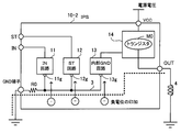
図2はIPSの構成例を示す図である。IPS10-1は、電源端子として、電源電圧が印加されるVCC端子と、GNDに接続されるGND端子(接地端子)とを有し、信号端子として、ST端子、IN端子および駆動信号を出力する出力端子OUTを有している。
また、IPS10-1は、内部回路として、IN回路(入力処理回路)11、ST回路(状態処理回路)12、内部GND回路13および駆動回路14を備える。
IN回路11の入力端は、IN端子に接続し、ST回路12の出力端は、ST端子に接続している。また、IN回路11、ST回路12および内部GND回路13それぞれのGND部(接地部)11g、12g、13gは、経路3を通じてGND端子に接続している。
IN回路11の入力端は、IN端子に接続し、ST回路12の出力端は、ST端子に接続している。また、IN回路11、ST回路12および内部GND回路13それぞれのGND部(接地部)11g、12g、13gは、経路3を通じてGND端子に接続している。
なお、以降においても、IPSの内部回路として、IN回路11、ST回路12、内部GND回路13および駆動回路14を示して説明するが、内部回路はこれらの回路に限定されるものでなく、他の内部回路であってもよい。
IN回路11は、IN端子から入力される入力信号を処理する回路である。ST回路12は、IPS10-1の各種状態を検出し、検出結果をST端子から出力する回路である。検出される状態としては、例えば、過電圧、過電流、過熱などがある。
内部GND回路13は、低電位の電圧を装置内部のGNDとして生成する回路である。生成された内部GNDは、IPS10-1内部の特定の回路に対して、GNDに代わる電位として供給される。例えば、図2では、内部GND回路13で生成された内部GNDは、駆動回路14に供給されている。
駆動回路14は、出力端子OUTに接続される、リレーやソレノイドなどのインダクタンス負荷4を駆動するための回路であり、出力段にパワートランジスタM0を有している。トランジスタM0は、例えば、MOSFET(Metal Oxide Semiconductor Field Effect Transistor)が使用される。なお、駆動回路14の詳細な構成および動作については図13で後述する。
(逆流電流の発生)
次に逆流電流の発生について説明する。図3は逆流電流の発生を示す図である。駆動回路14では、出力端子OUTに接続されているインダクタンス負荷4に対し、インダクタンス負荷4に流れる電流を、トランジスタM0によってオン・オフ制御している。
次に逆流電流の発生について説明する。図3は逆流電流の発生を示す図である。駆動回路14では、出力端子OUTに接続されているインダクタンス負荷4に対し、インダクタンス負荷4に流れる電流を、トランジスタM0によってオン・オフ制御している。
このような制御において、駆動回路14内のトランジスタM0がターンオフしたとき、インダクタンス負荷4に逆起電力が生じることにより、出力端子OUTが一時的に負電位になる場合がある。
出力端子OUTが負電位になると、GND端子が出力端子OUTよりも高電位になるから、GND端子から出力端子OUTに向かって、経路3上に逆流電流が流れることになる。
このとき、過大な逆流電流が流れると、経路3に接続している、IPS10-1の内部回路(IN回路11、ST回路12および内部GND回路13)が破壊に至るおそれがある。
(保護抵抗を備えたIPS)
次に逆流電流用の保護抵抗を備えたIPSについて説明する。図4はIPSの構成例を示す図である。IPS10-2は、図2で示した回路構成に対して、逆流電流から内部回路を保護するための保護抵抗R0をさらに備えた構成を有している。
次に逆流電流用の保護抵抗を備えたIPSについて説明する。図4はIPSの構成例を示す図である。IPS10-2は、図2で示した回路構成に対して、逆流電流から内部回路を保護するための保護抵抗R0をさらに備えた構成を有している。
保護抵抗R0は、経路3上に位置しており、保護抵抗R0の一端は、GND端子に接続する。また、保護抵抗R0の他端は、IN回路11のGND部11gと、ST回路12のGND部12gと、内部GND回路13のGND部13gと接続する。その他の構成は図2と同じである。
このような保護抵抗R0を設けることで、逆流電流が発生した場合でも、過大な逆流電流が内部回路に流れ込むことを抑制することができる。すなわち、出力端子OUTが負電位になって、GND端子から出力端子OUTへ逆流電流が流れる経路3が生じたとしても、保護抵抗R0によって、過大な逆流電流の流れを抑制することができ、素子破壊を防ぐことができる。
(負電位の印加)
次にIPSの内部回路に負電位が印加される状態について説明する。図5は内部回路に負電位が印加される状態を示す図である。図4で示したように、IPS10-2では、保護抵抗R0を設けている。これにより、IN回路11、ST回路12および内部GND回路13に対して、過大な逆流電流が流れ込むようなことはない。
次にIPSの内部回路に負電位が印加される状態について説明する。図5は内部回路に負電位が印加される状態を示す図である。図4で示したように、IPS10-2では、保護抵抗R0を設けている。これにより、IN回路11、ST回路12および内部GND回路13に対して、過大な逆流電流が流れ込むようなことはない。
ただし、このような構成では、IN回路11のGND部11g、ST回路12のGND部12gおよび内部GND回路13のGND部13gは、逆流電流が流れる経路3に直接接続していることになる。
この場合、出力端子OUTが負電位になると、IN回路11、ST回路12および内部GND回路13に対して、動作上不都合な負電位が印加されてしまう。
このような負電位は、トランジスタM0のターンオフ時のインダクタンス負荷4の逆起電力によって生じるものなので、一時的に発生するものであるが、たとえ一時的であっても負電位が印加されると、誤動作を引き起こす可能性がある。
このような負電位は、トランジスタM0のターンオフ時のインダクタンス負荷4の逆起電力によって生じるものなので、一時的に発生するものであるが、たとえ一時的であっても負電位が印加されると、誤動作を引き起こす可能性がある。
(第2の実施の形態)
次に内部回路に対し負電位が印加されないようにして、誤動作の防止を図った第2の実施の形態について説明する。
次に内部回路に対し負電位が印加されないようにして、誤動作の防止を図った第2の実施の形態について説明する。
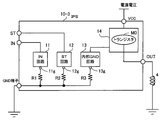
図6はIPSの構成例を示す図である。IPS10-3は、図2で示した回路構成に対して、さらに抵抗R1~R3を備えている。
抵抗R1の一端、抵抗R2の一端および抵抗R3の一端は、GND端子に接続する。また、抵抗R1の他端は、IN回路11のGND部11gに接続し、抵抗R2の他端は、ST回路12のGND部12gに接続する。さらに、抵抗R3の他端は、内部GND回路13のGND部13gの他端に接続する。その他の構成は図2と同じである。
抵抗R1の一端、抵抗R2の一端および抵抗R3の一端は、GND端子に接続する。また、抵抗R1の他端は、IN回路11のGND部11gに接続し、抵抗R2の他端は、ST回路12のGND部12gに接続する。さらに、抵抗R3の他端は、内部GND回路13のGND部13gの他端に接続する。その他の構成は図2と同じである。
このような抵抗R1~R3(以下、個別抵抗とも呼ぶ)を設けることで、IN回路11のGND部11g、ST回路12のGND部12gおよび内部GND回路13のGND部13gは、経路3に直接接続しなくなる。
したがって、出力端子OUTが負電位になっても、これらの内部回路に負電位が印加されるようなことはなく、誤動作の防止を図ることが可能になる。
また、内部回路に負電位が印加されないようにして誤動作の防止を図るだけでなく、過大な逆流電流の発生の抑制も図る場合には、抵抗R1~R3の合成抵抗値が、保護抵抗R0の値と同一になるような構成にすればよい。
また、内部回路に負電位が印加されないようにして誤動作の防止を図るだけでなく、過大な逆流電流の発生の抑制も図る場合には、抵抗R1~R3の合成抵抗値が、保護抵抗R0の値と同一になるような構成にすればよい。
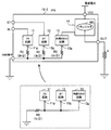
図7はIPSの構成例を示す図である。抵抗R1~R3の合成抵抗値が、図4で示した保護抵抗R0の値と同じになるように設定した構成例を示している。例えば、保護抵抗R0を1k[Ω]とすれば、3つの抵抗R1~R3は並列接続しているから、抵抗R1~R3それぞれの抵抗値を3k[Ω]とすればよい。
このように、複数の個別抵抗の合成抵抗値は、保護抵抗の抵抗値と同一にすれば、内部回路への負電位の印加防止だけでなく、過大な逆流電流が内部回路に流れ込むことも抑制することが可能になる。
(第3の実施の形態)
次に各内部回路の逆流電流の許容度合に応じて、抵抗R1~R3の抵抗値を適応的に変えて設定する第3の実施の形態の場合について説明する。
次に各内部回路の逆流電流の許容度合に応じて、抵抗R1~R3の抵抗値を適応的に変えて設定する第3の実施の形態の場合について説明する。
上記のように、個別抵抗の合成抵抗値を保護抵抗の抵抗値と同じにすれば、素子破壊に至るような過大な逆流電流の発生についても抑制することができる。
ただし、出力端子OUTが負電位になれば、GND端子から出力端子OUTに向かって、逆流電流が流れることには変わりはなく、抵抗を介して、内部回路には、素子破壊には至らなくてもある程度の逆流電流は流れ込むことになる。
ただし、出力端子OUTが負電位になれば、GND端子から出力端子OUTに向かって、逆流電流が流れることには変わりはなく、抵抗を介して、内部回路には、素子破壊には至らなくてもある程度の逆流電流は流れ込むことになる。
図7に示した構成では、個別抵抗の抵抗値はすべて同じ値に設定し、すべての内部回路に対して、同じ量の逆流電流が流れるようにしている。
これに対し、第3の実施の形態では、内部回路に流れ込む逆流電流の許容度合に応じて、個別抵抗の抵抗値を適応的に変えて設定する。ただし、内部回路毎に抵抗値の異なる個別抵抗を配置する場合であっても、過大な逆流電流が流れ込むことを抑制するために、それら個別抵抗の合成抵抗値と、保護抵抗の抵抗値とが同じ値になる条件は満たすようにする。
これに対し、第3の実施の形態では、内部回路に流れ込む逆流電流の許容度合に応じて、個別抵抗の抵抗値を適応的に変えて設定する。ただし、内部回路毎に抵抗値の異なる個別抵抗を配置する場合であっても、過大な逆流電流が流れ込むことを抑制するために、それら個別抵抗の合成抵抗値と、保護抵抗の抵抗値とが同じ値になる条件は満たすようにする。
以下、IN回路11、ST回路12および内部GND回路13の概略回路構成を示し、各回路に適した個別抵抗を設定する場合について説明する。
図8はIN回路の構成例を示す図である。IN回路11に個別抵抗R1が接続している状態での構成を示している。IN回路11は、ダイオードD1およびシュミットトリガタイプのインバータIC1を備える。
図8はIN回路の構成例を示す図である。IN回路11に個別抵抗R1が接続している状態での構成を示している。IN回路11は、ダイオードD1およびシュミットトリガタイプのインバータIC1を備える。
接続関係を記すと、IPSのIN端子は、インバータIC1の入力端と、ダイオードD1のカソードと接続する。インバータIC1の電源部は、電源電圧に接続し、インバータIC1の出力端子は、所定の回路素子に接続する。抵抗R1の一端は、経路3に接続し、抵抗R1の他端は、インバータIC1のGND部と、ダイオードD1のアノードと接続する。
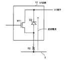
図9はST回路の構成例を示す図である。ST回路12に個別抵抗R2が接続している状態での構成を示している。ST回路12は、NMOSトランジスタM11、ダイオードD2を備える。
接続関係を記すと、トランジスタM11のゲートには、他回路から送信された信号が入力する。トランジスタM11のドレインは、IPSのST端子と、ダイオードD2のカソードと接続する。抵抗R2の一端は、経路3に接続し、抵抗R2の他端は、トランジスタM11のソースと、ダイオードD2のアノードと接続する。
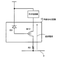
図10は内部GND回路の構成例を示す図である。内部GND回路13に個別抵抗R3が接続している状態での構成を示している。内部GND回路13は、PMOSトランジスタM12およびダイオードD3を備える。なお、図中のその他回路とは、例えば、図2に示した駆動回路14に該当する。
接続関係を記すと、ダイオードD3のカソードは、電源電圧と、その他回路の一端と接続し、ダイオードD3のアノードは、トランジスタM12のゲートに接続する。トランジスタM12のソースは、その他回路の他端と接続する。抵抗R3の一端は、経路3に接続し、抵抗R3の他端は、トランジスタM12のドレインと接続する。
ここで、図8に示したIN回路11では、逆流電流は、抵抗R1を介して、ダイオードD1を通過し、図9に示したST回路12では、逆流電流は、抵抗R2を介して、ダイオードD2を通過する。また、図10に示した内部GND回路13では、逆流電流は、抵抗R3を介して、トランジスタM12のドレインからソースへ抜けている。
このような逆流電流の流れにおいて、IN回路11やST回路12では、ダイオードの順方向に逆流電流が流れるので、内部GND回路13に流れる逆流電流に比べて、大きな逆流電流が流れ込みやすいといえる。逆に、内部GND回路13では、IN回路11やST回路12に流れる逆流電流に比べて、小さな逆流電流が流れるといえる。
大きな逆流電流が流れ込んでしまう可能性が高い内部回路に対しては、その内部回路に対して配置される個別抵抗の抵抗値を大きくして、逆流電流の流れ込みを、逆流電流が流れ込みにくい回路よりも強く制限する。
したがって、個別抵抗を適応的に設定する場合、IN回路11およびST回路12に対する抵抗R1、R2の抵抗値は、内部GND回路13の抵抗R3の抵抗値よりも大きく設定する。逆に、内部GND回路13に対する抵抗R3の値は、IN回路11およびST回路12の抵抗R1、R2の抵抗値よりも小さく設定する。すなわち、R1>R3、R2>R3となる。ただし、(1/R1)+(1/R2)+(1/R3)=R0の条件は満たすようにする。
(PN接合の面積に応じた個別抵抗値の設定)
次に内部回路に含まれるトランジスタのPN接合の面積に応じて、個別抵抗の抵抗値を適応的に設定する場合について説明する。なお、トランジスタの断面構成としては、NチャネルMOSFETの場合について説明する。
次に内部回路に含まれるトランジスタのPN接合の面積に応じて、個別抵抗の抵抗値を適応的に設定する場合について説明する。なお、トランジスタの断面構成としては、NチャネルMOSFETの場合について説明する。
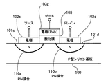
図11はNチャネルMOSFETの断面構成を示す図である。P型シリコン基板100にN型拡散層101s、101dが形成されている。また、N型拡散層101sから電極102sが引き出されてソースが形成され、N型拡散層101dから電極102dが引き出されてドレインが形成されている。
さらに、2つの対向するN型拡散層101s、101dの間の酸化膜(SiO2)103上に置かれたポリシリコン(多結晶シリコン)103gから電極を引き出してゲートが形成されている。
ちなみに、NチャネルMOSFETの場合、ゲートに正電位を印加すると、ゲート直下のP型シリコン基板の表面のP型拡散層がN型に反転し、これがソースとドレイン間で電流が流れる道(チャネル)として形成されることになる。
また、ゲートへの印加電圧が大きくなると、ドレイン-ソース間に電流が流れやすくなり、チャネルの長さが短くなるほど、またはゲート酸化膜の厚みが薄いほど、電流特性は向上することになる。
図11において、PN接合(半導体中でP型領域とN型領域とが接している部分)110a、110bの面積(表面積)が大きいトランジスタ程、そのトランジスタに流れる電流の許容量が高いので、逆流電流の許容度合も高いといえる。
したがって、逆流電流が流れ込む内部回路の中のライン上にトランジスタが存在し、そのトランジスタのPN接合の面積が大きい場合は、逆流電流の許容度が高い内部回路とみなせるので、該内部回路に配置する個別抵抗の抵抗値は小さく設定する。
または、逆流電流が流れ込む内部回路の中のライン上にトランジスタが存在し、そのトランジスタのPN接合の面積が小さい場合は、逆流電流の許容度が低い内部回路とみなせるので、該内部回路に配置する個別抵抗の抵抗値は大きく設定する。
このように、内部回路にトランジスタが含まれる場合、トランジスタのPN接合の面積に応じて個別抵抗の抵抗値を設定する。ただし、個別抵抗の合成抵抗値と、保護抵抗の抵抗値とが同じ値になる条件は満たすようにする。
(第4の実施の形態)
上記の実施の形態では、個別抵抗の一端は経路3に接続し、個別抵抗の他端は、1つの内部回路のGND部に接続することで、個別抵抗と、内部回路とが1対1の関係で配置される構成であった。
上記の実施の形態では、個別抵抗の一端は経路3に接続し、個別抵抗の他端は、1つの内部回路のGND部に接続することで、個別抵抗と、内部回路とが1対1の関係で配置される構成であった。
これに対し、第4の実施の形態は、個別抵抗の一端を経路3に接続し、個別抵抗の他端は、2つ以上の内部回路のGND部に接続することで、個別抵抗と、内部回路とが1対多の関係で配置するように構成したものである。
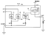
図12はIPSの構成例を示す図である。IPS10-4は、図2で示した回路構成に対して、さらに抵抗R4、R5を備えている。
抵抗R4の一端および抵抗R5の一端は、GND端子に接続する。抵抗R4の他端は、IN回路11のGND部11gと、ST回路12のGND部12gと接続する。抵抗R5の他端は、内部GND回路13のGND部13gの他端に接続する。その他の構成は図2と同じである。
抵抗R4の一端および抵抗R5の一端は、GND端子に接続する。抵抗R4の他端は、IN回路11のGND部11gと、ST回路12のGND部12gと接続する。抵抗R5の他端は、内部GND回路13のGND部13gの他端に接続する。その他の構成は図2と同じである。
このように、1つの個別抵抗の一端に複数の内部回路を接続してもよい。このような構成によっても、負電位の印加防止および過大な逆流電流の流れ込み抑制を実現することが可能になる。
(駆動回路)
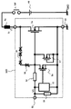
次に駆動回路の構成および動作について説明する。図13は駆動回路の構成例を示す図である。駆動回路500は、インダクタンス負荷の電流をオン・オフ制御する回路であり、インダクタンス負荷としてはソレノイドバルブ4aを示している。
次に駆動回路の構成および動作について説明する。図13は駆動回路の構成例を示す図である。駆動回路500は、インダクタンス負荷の電流をオン・オフ制御する回路であり、インダクタンス負荷としてはソレノイドバルブ4aを示している。
駆動回路500は、出力段MOSFET5a(図2のトランジスタM0に該当)、ゲート抵抗52および制御回路53を備える。また、遮断用MOSFET54、ダイナミッククランプダイオード55および逆流防止ダイオード56を備える。
ダイナミッククランプダイオード55は、直列接続された複数のツェナーダイオードにより構成されている。さらにプルダウンデプレッションMOSFET57、入力プルダウン抵抗58、GND端子59、入力端子50および出力端子51を備える。
入力端子50には、入力プルダウン抵抗58の一端と、制御回路53の高電位側と、ゲート抵抗52の一端が接続する。ゲート抵抗52の他端には、遮断用MOSFET54のドレインと、プルダウンデプレッションMOSFET57のドレインと、逆流防止ダイオード56のカソードおよび出力段MOSFET5aのゲートが接続する。また、制御回路53の出力側に、遮断用MOSFET54のゲートが接続する。
出力端子51には、出力段MOSFET5aのドレインと、ダイナミッククランプダイオード55のカソードが接続し、ダイナミッククランプダイオード55のアノードと、逆流防止ダイオード56のアノードが接続する。
GND端子59には、出力段MOSFET5aのソースと、プルダウンデプレッションMOSFET57のソースと、遮断用MOSFET54のソースと、制御回路53の低電位側および入力プルダウン抵抗58の他端が接続する。
動作について説明する。スイッチSWを導通させ、ソレノイドバルブ4aと出力段MOSFET5aに主電源V0の電圧を印加する(電源投入)。この電源投入時にはソレノイドバルブ4aは動作しない。
入力端子50に出力段MOSFET5aのゲートしきい値電圧Vth(例えば1.5V程度)の数倍の電圧(例えば5V程度)を印加する。
この電圧はゲート抵抗52を介して出力段MOSFET5aのゲートに正規のゲート電圧(例えば、5V程度)として印加される。そうすると、出力段MOSFET5aが導通してソレノイドバルブ4aに電流が流れて、ソレノイドバルブ4aが動作を開始する。
この電圧はゲート抵抗52を介して出力段MOSFET5aのゲートに正規のゲート電圧(例えば、5V程度)として印加される。そうすると、出力段MOSFET5aが導通してソレノイドバルブ4aに電流が流れて、ソレノイドバルブ4aが動作を開始する。
制御回路53は、コンパレータ、抵抗、ダイオードなどで構成された回路が内蔵され、入力端子50から入力される出力段MOSFET5aのゲート電圧を電源としている。
制御回路53は、出力段MOSFET5aのゲートしきい値電圧Vth以下の所定の電圧(例えば、1V程度)から動作するように設計されている。また、所定の電圧以上で、さらに出力段MOSFET5aのゲートしきい値電圧Vth以上の制御回路53で決められた電圧(制御回路のしきい値電圧Hと称し、例えば、H=2.5V程度である)以下では、遮断用MOSFET54がオンするゲート信号を出力するように設計されている。
制御回路53は、出力段MOSFET5aのゲートしきい値電圧Vth以下の所定の電圧(例えば、1V程度)から動作するように設計されている。また、所定の電圧以上で、さらに出力段MOSFET5aのゲートしきい値電圧Vth以上の制御回路53で決められた電圧(制御回路のしきい値電圧Hと称し、例えば、H=2.5V程度である)以下では、遮断用MOSFET54がオンするゲート信号を出力するように設計されている。
一方、制御回路53のしきい値電圧Hを超えた電圧では、遮断用MOSFET54がオフするゲート信号を出力するように設計されている。
入力端子50に制御回路53のしきい値電圧Hを超える信号V1が印加された場合、電圧V1をゲート抵抗52とプルダウンデプレッションMOSFET57のインピーダンスで分圧した電圧が、出力段MOSFET5aのゲートにゲート電圧として印加される。このゲート電圧が出力段MOSFET5aのゲートしきい値電圧Vth以上の場合は、出力段MOSFET5aが導通する。
入力端子50に制御回路53のしきい値電圧Hを超える信号V1が印加された場合、電圧V1をゲート抵抗52とプルダウンデプレッションMOSFET57のインピーダンスで分圧した電圧が、出力段MOSFET5aのゲートにゲート電圧として印加される。このゲート電圧が出力段MOSFET5aのゲートしきい値電圧Vth以上の場合は、出力段MOSFET5aが導通する。
プルダウンデプレッションMOSFET57の電圧・電流特性は、ゲートがGND電極に接続しており、ドレイン電流は数十μA程度で飽和する様に設計されている。そのため、数十μA程度以下ではドレイン電圧は低い電圧となる。
一方、ドレイン電流が数十μA程度以上ではドレイン電圧に依存せずにドレイン電流は一定になり、プルダウンデプレッションMOSFET57のインピーダンスは大きくなる。
出力段MOSFET5aの通常動作においては、プルダウンデプレッションMOSFET57のインピーダンスは、ゲート抵抗52に比べて極めて大きくなるため、入力端子50の電圧V1は、ゲート抵抗52で殆ど低下せずに、ほぼそのまま出力段MOSFET5aのゲートにゲート電圧として印加される。
一方、入力端子50に制御回路53のしきい値電圧H以下の信号が印加された場合は、制御回路53から出力される信号で遮断用MOSFET54が導通し、出力段MOSFET5aのゲート電圧を低下させる。
このゲート電圧が出力段MOSFET5aのゲートしきい値電圧Vthより低下すると出力段MOSFET5aは遮断する。
このように、出力段MOSFET5aのゲートしきい値電圧Vth以下の電圧でも制御回路53は正常に動作できるように設計されている。これにより、制御回路53のしきい値電圧Hを超える電圧が、入力端子50から制御回路53に入力されると、その電圧は出力段MOSFET5aのゲートしきい値電圧Vth以上であるので、出力段MOSFET5aは導通する。
このように、出力段MOSFET5aのゲートしきい値電圧Vth以下の電圧でも制御回路53は正常に動作できるように設計されている。これにより、制御回路53のしきい値電圧Hを超える電圧が、入力端子50から制御回路53に入力されると、その電圧は出力段MOSFET5aのゲートしきい値電圧Vth以上であるので、出力段MOSFET5aは導通する。
一方、制御回路53のしきい値電圧H(例えば、2.5V程度)以下の電圧が入力端子50から制御回路53に入力されると、この電圧は出力段MOSFET5aのゲートしきい値電圧Vth以上であるが、制御回路53からの信号で遮断用MOSFET54が導通するので、出力段MOSFET5aは遮断する。
つまり、入力端子50の電圧V1が制御回路53のしきい値電圧Hを超えると、出力段MOSFET5aは導通し、制御回路53のしきい値電圧H以下では、出力段MOSFET5aは導通しない。
このことから、出力段MOSFET5aの本来のゲートしきい値電圧Vthが、見かけ上、制御回路のしきい値電圧H(例えば、2.5V程度)に上昇したことになる。
次に電源投入時ではなく、出力段MOSFET5aが遮断したときについて説明する。図12において、ダイナミッククランプダイオード55は、出力段MOSFET5aを遮断した場合に、ソレノイドバルブ4aのインダクタンスにより発生する高電圧から出力段MOSFET5aを保護するためのものである。
次に電源投入時ではなく、出力段MOSFET5aが遮断したときについて説明する。図12において、ダイナミッククランプダイオード55は、出力段MOSFET5aを遮断した場合に、ソレノイドバルブ4aのインダクタンスにより発生する高電圧から出力段MOSFET5aを保護するためのものである。
このダイナミッククランプダイオード55に、クランプ電圧を超える高電圧が印加された場合、ダイナミッククランプダイオード55-逆流防止ダイオード56-ゲート抵抗52-入力プルダウン抵抗58-GND端子59の経路でサージ電流が流れる。
このサージ電流により、ゲート抵抗52および入力プルダウン抵抗58に電圧降下が発生する。この電圧降下により出力段MOSFET5aのゲート電圧を持ち上げられる。
ゲート電圧が出力段MOSFET5aのゲートしきい値電圧Vthを超えると、出力段MOSFET5aは導通する。この導通により、ソレノイドバルブ4aのインダクタンスに蓄えられたエネルギーは処理される。
ゲート電圧が出力段MOSFET5aのゲートしきい値電圧Vthを超えると、出力段MOSFET5aは導通する。この導通により、ソレノイドバルブ4aのインダクタンスに蓄えられたエネルギーは処理される。
なお、入力端子50に接続されるドライブ回路がオフ時に、低インピーダンスでGND電位にプルダウンする場合は、ゲート電圧を持ち上げるのは、ゲート抵抗52の電圧降下となる。
駆動回路500では、制御回路53の電源は、入力端子50から入力される電圧V1(信号電圧)を用いている。そのため、この制御回路53は、個別の制御用電源を必要とせず、駆動回路500は、見かけ上、3端子のMOSFETと同等の動作をする。
ここで、GND端子59は、MOSFETのソース端子、入力端子50はゲート端子、出力端子51はドレイン端子にそれぞれ相当する。また、制御回路53と同様に電圧V1を電源とする、図示しない電流制限回路や過電流保護回路などを駆動回路500に付加することにより、保護機能などを持つ3端子の高機能MOSFETとして使用することができる。
以上、実施の形態を例示したが、実施の形態で示した各部の構成は同様の機能を有する他のものに置換することができる。また、他の任意の構成物や工程が付加されてもよい。
上記については単に本発明の原理を示すものである。さらに、多数の変形、変更が当業者にとって可能であり、本発明は上記に示し、説明した正確な構成および応用例に限定されるものではなく、対応するすべての変形例および均等物は、添付の請求項およびその均等物による本発明の範囲とみなされる。
上記については単に本発明の原理を示すものである。さらに、多数の変形、変更が当業者にとって可能であり、本発明は上記に示し、説明した正確な構成および応用例に限定されるものではなく、対応するすべての変形例および均等物は、添付の請求項およびその均等物による本発明の範囲とみなされる。
1 半導体装置
1-1、1-n 内部回路
1a 接地端子
1b 出力端子
2-1、2-n 接地部
3a 経路
R1、Rn 抵抗
1-1、1-n 内部回路
1a 接地端子
1b 出力端子
2-1、2-n 接地部
3a 経路
R1、Rn 抵抗
Claims (7)
- 装置内に実装された内部回路と、
当該装置を接地する接地端子につながる経路と、前記内部回路との間に配置される抵抗と、
を備え、
当該装置の出力端子が負電位になることで前記接地端子から前記出力端子に向かって逆流電流が流れる前記経路であって、前記抵抗の一端は、前記経路に接続し、前記抵抗の他端は、前記内部回路の接地部に接続する、
ことを特徴とする半導体装置。 - 前記抵抗の他端が、1つの前記内部回路の前記接地部に接続して、前記抵抗と、前記内部回路とが1対1の関係で配置されることを特徴とする請求項1記載の半導体装置。
- 複数の前記抵抗の合成抵抗値は、
前記経路上に位置し、一端を前記接地端子と接続し、他端を複数の前記内部回路の前記接地部に接続して、前記逆流電流に対して前記内部回路を保護するために設けられた保護抵抗の抵抗値と同一であることを特徴とする請求項1記載の半導体装置。 - 複数の前記抵抗の合成抵抗値が、前記保護抵抗の抵抗値と同一であるという条件を満たした上で、複数の前記抵抗の個々の抵抗値は、前記抵抗が接続される前記内部回路の前記逆流電流の許容度合にもとづいて適応的に設定されることを特徴とする請求項3記載の半導体装置。
- 前記内部回路にトランジスタが含まれる場合、前記トランジスタのPN接合の面積に応じて前記抵抗の抵抗値が設定されることを特徴とする請求項4記載の半導体装置。
- 前記抵抗の一端は、前記経路に接続し、前記抵抗の他端は、2つ以上の前記内部回路の前記接地部に接続して、前記抵抗と、前記内部回路とが1対多の関係で配置されることを特徴とする請求項1記載の半導体装置。
- 半導体装置の負電位印加防止方法において、
前記半導体装置を接地する接地端子につながる経路に、前記半導体装置の出力端子が負電位になることで前記接地端子から前記出力端子に向かって逆流電流が流れる場合に、
前記経路と、前記半導体装置内に実装された内部回路との間に抵抗を配置し、
前記抵抗の一端を、前記経路に接続し、
前記抵抗の他端を、前記内部回路の接地部に接続する、
ことを特徴とする負電位印加防止方法。
Priority Applications (1)
| Application Number | Priority Date | Filing Date | Title |
|---|---|---|---|
| JP2016560116A JP6222381B2 (ja) | 2014-11-21 | 2015-10-16 | 半導体装置および負電位印加防止方法 |
Applications Claiming Priority (2)
| Application Number | Priority Date | Filing Date | Title |
|---|---|---|---|
| JP2014236260 | 2014-11-21 | ||
| JP2014-236260 | 2014-11-21 |
Publications (1)
| Publication Number | Publication Date |
|---|---|
| WO2016080123A1 true WO2016080123A1 (ja) | 2016-05-26 |
Family
ID=56013680
Family Applications (1)
| Application Number | Title | Priority Date | Filing Date |
|---|---|---|---|
| PCT/JP2015/079287 Ceased WO2016080123A1 (ja) | 2014-11-21 | 2015-10-16 | 半導体装置および負電位印加防止方法 |
Country Status (2)
| Country | Link |
|---|---|
| JP (1) | JP6222381B2 (ja) |
| WO (1) | WO2016080123A1 (ja) |
Cited By (1)
| Publication number | Priority date | Publication date | Assignee | Title |
|---|---|---|---|---|
| JP2022147315A (ja) * | 2021-03-23 | 2022-10-06 | 株式会社アイシン | 誘導性負荷駆動装置 |
Citations (4)
| Publication number | Priority date | Publication date | Assignee | Title |
|---|---|---|---|---|
| JPH0690520A (ja) * | 1992-09-09 | 1994-03-29 | Toshiba Corp | 誤動作防止回路および保護回路 |
| JP2009010477A (ja) * | 2007-06-26 | 2009-01-15 | Nec Electronics Corp | 半導体装置 |
| JP2012034079A (ja) * | 2010-07-29 | 2012-02-16 | Fuji Electric Co Ltd | 絶縁ゲート型デバイスの駆動回路 |
| JP2013146008A (ja) * | 2012-01-16 | 2013-07-25 | Fuji Electric Co Ltd | 駆動回路およびパワー集積回路装置 |
-
2015
- 2015-10-16 JP JP2016560116A patent/JP6222381B2/ja active Active
- 2015-10-16 WO PCT/JP2015/079287 patent/WO2016080123A1/ja not_active Ceased
Patent Citations (4)
| Publication number | Priority date | Publication date | Assignee | Title |
|---|---|---|---|---|
| JPH0690520A (ja) * | 1992-09-09 | 1994-03-29 | Toshiba Corp | 誤動作防止回路および保護回路 |
| JP2009010477A (ja) * | 2007-06-26 | 2009-01-15 | Nec Electronics Corp | 半導体装置 |
| JP2012034079A (ja) * | 2010-07-29 | 2012-02-16 | Fuji Electric Co Ltd | 絶縁ゲート型デバイスの駆動回路 |
| JP2013146008A (ja) * | 2012-01-16 | 2013-07-25 | Fuji Electric Co Ltd | 駆動回路およびパワー集積回路装置 |
Cited By (2)
| Publication number | Priority date | Publication date | Assignee | Title |
|---|---|---|---|---|
| JP2022147315A (ja) * | 2021-03-23 | 2022-10-06 | 株式会社アイシン | 誘導性負荷駆動装置 |
| JP7729056B2 (ja) | 2021-03-23 | 2025-08-26 | 株式会社アイシン | 誘導性負荷駆動装置 |
Also Published As
| Publication number | Publication date |
|---|---|
| JPWO2016080123A1 (ja) | 2017-04-27 |
| JP6222381B2 (ja) | 2017-11-01 |
Similar Documents
| Publication | Publication Date | Title |
|---|---|---|
| US10381827B2 (en) | Semiconductor integrated circuit device | |
| KR101870995B1 (ko) | 반도체 집적회로의 esd 보호 회로 | |
| US7755870B2 (en) | Semiconductor integrated circuit device | |
| US20140368958A1 (en) | Electrostatic protection circuit | |
| US20140307354A1 (en) | Esd protection circuit | |
| JP2018064082A (ja) | 静電放電回路 | |
| JP2009147995A (ja) | 電力供給制御回路 | |
| US7394631B2 (en) | Electrostatic protection circuit | |
| EP2066032A2 (en) | Power supply control circuit including overvoltage protection circuit | |
| US8937793B2 (en) | Semiconductor device | |
| JP2014026996A (ja) | Esd保護回路 | |
| JP2002313949A (ja) | 過電圧保護回路 | |
| CN105957863A (zh) | 静电保护电路 | |
| US20150256166A1 (en) | Voltage selection circuit and semiconductor integrated circuit device having the same | |
| US20100053827A1 (en) | Protection circuit | |
| US7643258B2 (en) | Methods and apparatus for electrostatic discharge protection in a semiconductor circuit | |
| WO2015114923A1 (ja) | 半導体集積回路装置 | |
| US7456441B2 (en) | Single well excess current dissipation circuit | |
| JP2009170452A (ja) | 電力スイッチ回路 | |
| JP6222381B2 (ja) | 半導体装置および負電位印加防止方法 | |
| JP6405986B2 (ja) | 静電気保護回路及び半導体集積回路装置 | |
| US9154133B2 (en) | ESD robust level shifter | |
| JP6277151B2 (ja) | センサ装置 | |
| JP5915246B2 (ja) | 保護回路および半導体集積回路 | |
| JP5010158B2 (ja) | 半導体装置 |
Legal Events
| Date | Code | Title | Description |
|---|---|---|---|
| 121 | Ep: the epo has been informed by wipo that ep was designated in this application |
Ref document number: 15861345 Country of ref document: EP Kind code of ref document: A1 |
|
| ENP | Entry into the national phase |
Ref document number: 2016560116 Country of ref document: JP Kind code of ref document: A |
|
| NENP | Non-entry into the national phase |
Ref country code: DE |
|
| 122 | Ep: pct application non-entry in european phase |
Ref document number: 15861345 Country of ref document: EP Kind code of ref document: A1 |