WO2016068169A1 - 異方性導電フィルム及び接続構造体 - Google Patents
異方性導電フィルム及び接続構造体 Download PDFInfo
- Publication number
- WO2016068169A1 WO2016068169A1 PCT/JP2015/080338 JP2015080338W WO2016068169A1 WO 2016068169 A1 WO2016068169 A1 WO 2016068169A1 JP 2015080338 W JP2015080338 W JP 2015080338W WO 2016068169 A1 WO2016068169 A1 WO 2016068169A1
- Authority
- WO
- WIPO (PCT)
- Prior art keywords
- conductive
- conductive particles
- particles
- particle
- conductive film
- Prior art date
Links
Images


Classifications
-
- H—ELECTRICITY
- H01—ELECTRIC ELEMENTS
- H01B—CABLES; CONDUCTORS; INSULATORS; SELECTION OF MATERIALS FOR THEIR CONDUCTIVE, INSULATING OR DIELECTRIC PROPERTIES
- H01B5/00—Non-insulated conductors or conductive bodies characterised by their form
- H01B5/16—Non-insulated conductors or conductive bodies characterised by their form comprising conductive material in insulating or poorly conductive material, e.g. conductive rubber
-
- H—ELECTRICITY
- H01—ELECTRIC ELEMENTS
- H01L—SEMICONDUCTOR DEVICES NOT COVERED BY CLASS H10
- H01L24/00—Arrangements for connecting or disconnecting semiconductor or solid-state bodies; Methods or apparatus related thereto
- H01L24/01—Means for bonding being attached to, or being formed on, the surface to be connected, e.g. chip-to-package, die-attach, "first-level" interconnects; Manufacturing methods related thereto
- H01L24/26—Layer connectors, e.g. plate connectors, solder or adhesive layers; Manufacturing methods related thereto
- H01L24/31—Structure, shape, material or disposition of the layer connectors after the connecting process
- H01L24/32—Structure, shape, material or disposition of the layer connectors after the connecting process of an individual layer connector
-
- C—CHEMISTRY; METALLURGY
- C09—DYES; PAINTS; POLISHES; NATURAL RESINS; ADHESIVES; COMPOSITIONS NOT OTHERWISE PROVIDED FOR; APPLICATIONS OF MATERIALS NOT OTHERWISE PROVIDED FOR
- C09J—ADHESIVES; NON-MECHANICAL ASPECTS OF ADHESIVE PROCESSES IN GENERAL; ADHESIVE PROCESSES NOT PROVIDED FOR ELSEWHERE; USE OF MATERIALS AS ADHESIVES
- C09J7/00—Adhesives in the form of films or foils
- C09J7/10—Adhesives in the form of films or foils without carriers
-
- C—CHEMISTRY; METALLURGY
- C09—DYES; PAINTS; POLISHES; NATURAL RESINS; ADHESIVES; COMPOSITIONS NOT OTHERWISE PROVIDED FOR; APPLICATIONS OF MATERIALS NOT OTHERWISE PROVIDED FOR
- C09J—ADHESIVES; NON-MECHANICAL ASPECTS OF ADHESIVE PROCESSES IN GENERAL; ADHESIVE PROCESSES NOT PROVIDED FOR ELSEWHERE; USE OF MATERIALS AS ADHESIVES
- C09J9/00—Adhesives characterised by their physical nature or the effects produced, e.g. glue sticks
- C09J9/02—Electrically-conducting adhesives
-
- H—ELECTRICITY
- H01—ELECTRIC ELEMENTS
- H01B—CABLES; CONDUCTORS; INSULATORS; SELECTION OF MATERIALS FOR THEIR CONDUCTIVE, INSULATING OR DIELECTRIC PROPERTIES
- H01B1/00—Conductors or conductive bodies characterised by the conductive materials; Selection of materials as conductors
- H01B1/02—Conductors or conductive bodies characterised by the conductive materials; Selection of materials as conductors mainly consisting of metals or alloys
-
- H—ELECTRICITY
- H01—ELECTRIC ELEMENTS
- H01L—SEMICONDUCTOR DEVICES NOT COVERED BY CLASS H10
- H01L24/00—Arrangements for connecting or disconnecting semiconductor or solid-state bodies; Methods or apparatus related thereto
- H01L24/01—Means for bonding being attached to, or being formed on, the surface to be connected, e.g. chip-to-package, die-attach, "first-level" interconnects; Manufacturing methods related thereto
- H01L24/26—Layer connectors, e.g. plate connectors, solder or adhesive layers; Manufacturing methods related thereto
- H01L24/27—Manufacturing methods
-
- H—ELECTRICITY
- H01—ELECTRIC ELEMENTS
- H01L—SEMICONDUCTOR DEVICES NOT COVERED BY CLASS H10
- H01L24/00—Arrangements for connecting or disconnecting semiconductor or solid-state bodies; Methods or apparatus related thereto
- H01L24/01—Means for bonding being attached to, or being formed on, the surface to be connected, e.g. chip-to-package, die-attach, "first-level" interconnects; Manufacturing methods related thereto
- H01L24/26—Layer connectors, e.g. plate connectors, solder or adhesive layers; Manufacturing methods related thereto
- H01L24/28—Structure, shape, material or disposition of the layer connectors prior to the connecting process
- H01L24/29—Structure, shape, material or disposition of the layer connectors prior to the connecting process of an individual layer connector
-
- H—ELECTRICITY
- H01—ELECTRIC ELEMENTS
- H01L—SEMICONDUCTOR DEVICES NOT COVERED BY CLASS H10
- H01L24/00—Arrangements for connecting or disconnecting semiconductor or solid-state bodies; Methods or apparatus related thereto
- H01L24/80—Methods for connecting semiconductor or other solid state bodies using means for bonding being attached to, or being formed on, the surface to be connected
- H01L24/83—Methods for connecting semiconductor or other solid state bodies using means for bonding being attached to, or being formed on, the surface to be connected using a layer connector
-
- H—ELECTRICITY
- H01—ELECTRIC ELEMENTS
- H01R—ELECTRICALLY-CONDUCTIVE CONNECTIONS; STRUCTURAL ASSOCIATIONS OF A PLURALITY OF MUTUALLY-INSULATED ELECTRICAL CONNECTING ELEMENTS; COUPLING DEVICES; CURRENT COLLECTORS
- H01R11/00—Individual connecting elements providing two or more spaced connecting locations for conductive members which are, or may be, thereby interconnected, e.g. end pieces for wires or cables supported by the wire or cable and having means for facilitating electrical connection to some other wire, terminal, or conductive member, blocks of binding posts
- H01R11/01—Individual connecting elements providing two or more spaced connecting locations for conductive members which are, or may be, thereby interconnected, e.g. end pieces for wires or cables supported by the wire or cable and having means for facilitating electrical connection to some other wire, terminal, or conductive member, blocks of binding posts characterised by the form or arrangement of the conductive interconnection between the connecting locations
-
- C—CHEMISTRY; METALLURGY
- C08—ORGANIC MACROMOLECULAR COMPOUNDS; THEIR PREPARATION OR CHEMICAL WORKING-UP; COMPOSITIONS BASED THEREON
- C08K—Use of inorganic or non-macromolecular organic substances as compounding ingredients
- C08K2201/00—Specific properties of additives
- C08K2201/001—Conductive additives
-
- C—CHEMISTRY; METALLURGY
- C08—ORGANIC MACROMOLECULAR COMPOUNDS; THEIR PREPARATION OR CHEMICAL WORKING-UP; COMPOSITIONS BASED THEREON
- C08K—Use of inorganic or non-macromolecular organic substances as compounding ingredients
- C08K3/00—Use of inorganic substances as compounding ingredients
- C08K3/02—Elements
- C08K3/08—Metals
-
- C—CHEMISTRY; METALLURGY
- C08—ORGANIC MACROMOLECULAR COMPOUNDS; THEIR PREPARATION OR CHEMICAL WORKING-UP; COMPOSITIONS BASED THEREON
- C08K—Use of inorganic or non-macromolecular organic substances as compounding ingredients
- C08K9/00—Use of pretreated ingredients
- C08K9/02—Ingredients treated with inorganic substances
-
- C—CHEMISTRY; METALLURGY
- C09—DYES; PAINTS; POLISHES; NATURAL RESINS; ADHESIVES; COMPOSITIONS NOT OTHERWISE PROVIDED FOR; APPLICATIONS OF MATERIALS NOT OTHERWISE PROVIDED FOR
- C09J—ADHESIVES; NON-MECHANICAL ASPECTS OF ADHESIVE PROCESSES IN GENERAL; ADHESIVE PROCESSES NOT PROVIDED FOR ELSEWHERE; USE OF MATERIALS AS ADHESIVES
- C09J2203/00—Applications of adhesives in processes or use of adhesives in the form of films or foils
- C09J2203/326—Applications of adhesives in processes or use of adhesives in the form of films or foils for bonding electronic components such as wafers, chips or semiconductors
-
- C—CHEMISTRY; METALLURGY
- C09—DYES; PAINTS; POLISHES; NATURAL RESINS; ADHESIVES; COMPOSITIONS NOT OTHERWISE PROVIDED FOR; APPLICATIONS OF MATERIALS NOT OTHERWISE PROVIDED FOR
- C09J—ADHESIVES; NON-MECHANICAL ASPECTS OF ADHESIVE PROCESSES IN GENERAL; ADHESIVE PROCESSES NOT PROVIDED FOR ELSEWHERE; USE OF MATERIALS AS ADHESIVES
- C09J2301/00—Additional features of adhesives in the form of films or foils
- C09J2301/30—Additional features of adhesives in the form of films or foils characterized by the chemical, physicochemical or physical properties of the adhesive or the carrier
- C09J2301/314—Additional features of adhesives in the form of films or foils characterized by the chemical, physicochemical or physical properties of the adhesive or the carrier the adhesive layer and/or the carrier being conductive
-
- C—CHEMISTRY; METALLURGY
- C09—DYES; PAINTS; POLISHES; NATURAL RESINS; ADHESIVES; COMPOSITIONS NOT OTHERWISE PROVIDED FOR; APPLICATIONS OF MATERIALS NOT OTHERWISE PROVIDED FOR
- C09J—ADHESIVES; NON-MECHANICAL ASPECTS OF ADHESIVE PROCESSES IN GENERAL; ADHESIVE PROCESSES NOT PROVIDED FOR ELSEWHERE; USE OF MATERIALS AS ADHESIVES
- C09J2301/00—Additional features of adhesives in the form of films or foils
- C09J2301/40—Additional features of adhesives in the form of films or foils characterized by the presence of essential components
- C09J2301/408—Additional features of adhesives in the form of films or foils characterized by the presence of essential components additives as essential feature of the adhesive layer
-
- H—ELECTRICITY
- H01—ELECTRIC ELEMENTS
- H01B—CABLES; CONDUCTORS; INSULATORS; SELECTION OF MATERIALS FOR THEIR CONDUCTIVE, INSULATING OR DIELECTRIC PROPERTIES
- H01B1/00—Conductors or conductive bodies characterised by the conductive materials; Selection of materials as conductors
- H01B1/20—Conductive material dispersed in non-conductive organic material
- H01B1/22—Conductive material dispersed in non-conductive organic material the conductive material comprising metals or alloys
-
- H—ELECTRICITY
- H01—ELECTRIC ELEMENTS
- H01L—SEMICONDUCTOR DEVICES NOT COVERED BY CLASS H10
- H01L2224/00—Indexing scheme for arrangements for connecting or disconnecting semiconductor or solid-state bodies and methods related thereto as covered by H01L24/00
- H01L2224/01—Means for bonding being attached to, or being formed on, the surface to be connected, e.g. chip-to-package, die-attach, "first-level" interconnects; Manufacturing methods related thereto
- H01L2224/10—Bump connectors; Manufacturing methods related thereto
- H01L2224/12—Structure, shape, material or disposition of the bump connectors prior to the connecting process
- H01L2224/13—Structure, shape, material or disposition of the bump connectors prior to the connecting process of an individual bump connector
- H01L2224/1354—Coating
- H01L2224/13599—Material
- H01L2224/136—Material with a principal constituent of the material being a metal or a metalloid, e.g. boron [B], silicon [Si], germanium [Ge], arsenic [As], antimony [Sb], tellurium [Te] and polonium [Po], and alloys thereof
- H01L2224/13638—Material with a principal constituent of the material being a metal or a metalloid, e.g. boron [B], silicon [Si], germanium [Ge], arsenic [As], antimony [Sb], tellurium [Te] and polonium [Po], and alloys thereof the principal constituent melting at a temperature of greater than or equal to 950°C and less than 1550°C
- H01L2224/13644—Gold [Au] as principal constituent
-
- H—ELECTRICITY
- H01—ELECTRIC ELEMENTS
- H01L—SEMICONDUCTOR DEVICES NOT COVERED BY CLASS H10
- H01L2224/00—Indexing scheme for arrangements for connecting or disconnecting semiconductor or solid-state bodies and methods related thereto as covered by H01L24/00
- H01L2224/01—Means for bonding being attached to, or being formed on, the surface to be connected, e.g. chip-to-package, die-attach, "first-level" interconnects; Manufacturing methods related thereto
- H01L2224/26—Layer connectors, e.g. plate connectors, solder or adhesive layers; Manufacturing methods related thereto
- H01L2224/27—Manufacturing methods
- H01L2224/27001—Involving a temporary auxiliary member not forming part of the manufacturing apparatus, e.g. removable or sacrificial coating, film or substrate
- H01L2224/27003—Involving a temporary auxiliary member not forming part of the manufacturing apparatus, e.g. removable or sacrificial coating, film or substrate for holding or transferring the layer preform
-
- H—ELECTRICITY
- H01—ELECTRIC ELEMENTS
- H01L—SEMICONDUCTOR DEVICES NOT COVERED BY CLASS H10
- H01L2224/00—Indexing scheme for arrangements for connecting or disconnecting semiconductor or solid-state bodies and methods related thereto as covered by H01L24/00
- H01L2224/01—Means for bonding being attached to, or being formed on, the surface to be connected, e.g. chip-to-package, die-attach, "first-level" interconnects; Manufacturing methods related thereto
- H01L2224/26—Layer connectors, e.g. plate connectors, solder or adhesive layers; Manufacturing methods related thereto
- H01L2224/27—Manufacturing methods
- H01L2224/271—Manufacture and pre-treatment of the layer connector preform
- H01L2224/2711—Shaping
-
- H—ELECTRICITY
- H01—ELECTRIC ELEMENTS
- H01L—SEMICONDUCTOR DEVICES NOT COVERED BY CLASS H10
- H01L2224/00—Indexing scheme for arrangements for connecting or disconnecting semiconductor or solid-state bodies and methods related thereto as covered by H01L24/00
- H01L2224/01—Means for bonding being attached to, or being formed on, the surface to be connected, e.g. chip-to-package, die-attach, "first-level" interconnects; Manufacturing methods related thereto
- H01L2224/26—Layer connectors, e.g. plate connectors, solder or adhesive layers; Manufacturing methods related thereto
- H01L2224/27—Manufacturing methods
- H01L2224/274—Manufacturing methods by blanket deposition of the material of the layer connector
- H01L2224/2746—Plating
- H01L2224/27462—Electroplating
-
- H—ELECTRICITY
- H01—ELECTRIC ELEMENTS
- H01L—SEMICONDUCTOR DEVICES NOT COVERED BY CLASS H10
- H01L2224/00—Indexing scheme for arrangements for connecting or disconnecting semiconductor or solid-state bodies and methods related thereto as covered by H01L24/00
- H01L2224/01—Means for bonding being attached to, or being formed on, the surface to be connected, e.g. chip-to-package, die-attach, "first-level" interconnects; Manufacturing methods related thereto
- H01L2224/26—Layer connectors, e.g. plate connectors, solder or adhesive layers; Manufacturing methods related thereto
- H01L2224/27—Manufacturing methods
- H01L2224/274—Manufacturing methods by blanket deposition of the material of the layer connector
- H01L2224/2746—Plating
- H01L2224/27464—Electroless plating
-
- H—ELECTRICITY
- H01—ELECTRIC ELEMENTS
- H01L—SEMICONDUCTOR DEVICES NOT COVERED BY CLASS H10
- H01L2224/00—Indexing scheme for arrangements for connecting or disconnecting semiconductor or solid-state bodies and methods related thereto as covered by H01L24/00
- H01L2224/01—Means for bonding being attached to, or being formed on, the surface to be connected, e.g. chip-to-package, die-attach, "first-level" interconnects; Manufacturing methods related thereto
- H01L2224/26—Layer connectors, e.g. plate connectors, solder or adhesive layers; Manufacturing methods related thereto
- H01L2224/28—Structure, shape, material or disposition of the layer connectors prior to the connecting process
- H01L2224/29—Structure, shape, material or disposition of the layer connectors prior to the connecting process of an individual layer connector
- H01L2224/29001—Core members of the layer connector
- H01L2224/29099—Material
- H01L2224/29198—Material with a principal constituent of the material being a combination of two or more materials in the form of a matrix with a filler, i.e. being a hybrid material, e.g. segmented structures, foams
- H01L2224/29199—Material of the matrix
- H01L2224/2929—Material of the matrix with a principal constituent of the material being a polymer, e.g. polyester, phenolic based polymer, epoxy
-
- H—ELECTRICITY
- H01—ELECTRIC ELEMENTS
- H01L—SEMICONDUCTOR DEVICES NOT COVERED BY CLASS H10
- H01L2224/00—Indexing scheme for arrangements for connecting or disconnecting semiconductor or solid-state bodies and methods related thereto as covered by H01L24/00
- H01L2224/01—Means for bonding being attached to, or being formed on, the surface to be connected, e.g. chip-to-package, die-attach, "first-level" interconnects; Manufacturing methods related thereto
- H01L2224/26—Layer connectors, e.g. plate connectors, solder or adhesive layers; Manufacturing methods related thereto
- H01L2224/28—Structure, shape, material or disposition of the layer connectors prior to the connecting process
- H01L2224/29—Structure, shape, material or disposition of the layer connectors prior to the connecting process of an individual layer connector
- H01L2224/29001—Core members of the layer connector
- H01L2224/29099—Material
- H01L2224/29198—Material with a principal constituent of the material being a combination of two or more materials in the form of a matrix with a filler, i.e. being a hybrid material, e.g. segmented structures, foams
- H01L2224/29298—Fillers
- H01L2224/29299—Base material
- H01L2224/293—Base material with a principal constituent of the material being a metal or a metalloid, e.g. boron [B], silicon [Si], germanium [Ge], arsenic [As], antimony [Sb], tellurium [Te] and polonium [Po], and alloys thereof
- H01L2224/29338—Base material with a principal constituent of the material being a metal or a metalloid, e.g. boron [B], silicon [Si], germanium [Ge], arsenic [As], antimony [Sb], tellurium [Te] and polonium [Po], and alloys thereof the principal constituent melting at a temperature of greater than or equal to 950°C and less than 1550°C
- H01L2224/29339—Silver [Ag] as principal constituent
-
- H—ELECTRICITY
- H01—ELECTRIC ELEMENTS
- H01L—SEMICONDUCTOR DEVICES NOT COVERED BY CLASS H10
- H01L2224/00—Indexing scheme for arrangements for connecting or disconnecting semiconductor or solid-state bodies and methods related thereto as covered by H01L24/00
- H01L2224/01—Means for bonding being attached to, or being formed on, the surface to be connected, e.g. chip-to-package, die-attach, "first-level" interconnects; Manufacturing methods related thereto
- H01L2224/26—Layer connectors, e.g. plate connectors, solder or adhesive layers; Manufacturing methods related thereto
- H01L2224/28—Structure, shape, material or disposition of the layer connectors prior to the connecting process
- H01L2224/29—Structure, shape, material or disposition of the layer connectors prior to the connecting process of an individual layer connector
- H01L2224/29001—Core members of the layer connector
- H01L2224/29099—Material
- H01L2224/29198—Material with a principal constituent of the material being a combination of two or more materials in the form of a matrix with a filler, i.e. being a hybrid material, e.g. segmented structures, foams
- H01L2224/29298—Fillers
- H01L2224/29299—Base material
- H01L2224/293—Base material with a principal constituent of the material being a metal or a metalloid, e.g. boron [B], silicon [Si], germanium [Ge], arsenic [As], antimony [Sb], tellurium [Te] and polonium [Po], and alloys thereof
- H01L2224/29338—Base material with a principal constituent of the material being a metal or a metalloid, e.g. boron [B], silicon [Si], germanium [Ge], arsenic [As], antimony [Sb], tellurium [Te] and polonium [Po], and alloys thereof the principal constituent melting at a temperature of greater than or equal to 950°C and less than 1550°C
- H01L2224/29344—Gold [Au] as principal constituent
-
- H—ELECTRICITY
- H01—ELECTRIC ELEMENTS
- H01L—SEMICONDUCTOR DEVICES NOT COVERED BY CLASS H10
- H01L2224/00—Indexing scheme for arrangements for connecting or disconnecting semiconductor or solid-state bodies and methods related thereto as covered by H01L24/00
- H01L2224/01—Means for bonding being attached to, or being formed on, the surface to be connected, e.g. chip-to-package, die-attach, "first-level" interconnects; Manufacturing methods related thereto
- H01L2224/26—Layer connectors, e.g. plate connectors, solder or adhesive layers; Manufacturing methods related thereto
- H01L2224/28—Structure, shape, material or disposition of the layer connectors prior to the connecting process
- H01L2224/29—Structure, shape, material or disposition of the layer connectors prior to the connecting process of an individual layer connector
- H01L2224/29001—Core members of the layer connector
- H01L2224/29099—Material
- H01L2224/29198—Material with a principal constituent of the material being a combination of two or more materials in the form of a matrix with a filler, i.e. being a hybrid material, e.g. segmented structures, foams
- H01L2224/29298—Fillers
- H01L2224/29299—Base material
- H01L2224/293—Base material with a principal constituent of the material being a metal or a metalloid, e.g. boron [B], silicon [Si], germanium [Ge], arsenic [As], antimony [Sb], tellurium [Te] and polonium [Po], and alloys thereof
- H01L2224/29338—Base material with a principal constituent of the material being a metal or a metalloid, e.g. boron [B], silicon [Si], germanium [Ge], arsenic [As], antimony [Sb], tellurium [Te] and polonium [Po], and alloys thereof the principal constituent melting at a temperature of greater than or equal to 950°C and less than 1550°C
- H01L2224/29347—Copper [Cu] as principal constituent
-
- H—ELECTRICITY
- H01—ELECTRIC ELEMENTS
- H01L—SEMICONDUCTOR DEVICES NOT COVERED BY CLASS H10
- H01L2224/00—Indexing scheme for arrangements for connecting or disconnecting semiconductor or solid-state bodies and methods related thereto as covered by H01L24/00
- H01L2224/01—Means for bonding being attached to, or being formed on, the surface to be connected, e.g. chip-to-package, die-attach, "first-level" interconnects; Manufacturing methods related thereto
- H01L2224/26—Layer connectors, e.g. plate connectors, solder or adhesive layers; Manufacturing methods related thereto
- H01L2224/28—Structure, shape, material or disposition of the layer connectors prior to the connecting process
- H01L2224/29—Structure, shape, material or disposition of the layer connectors prior to the connecting process of an individual layer connector
- H01L2224/29001—Core members of the layer connector
- H01L2224/29099—Material
- H01L2224/29198—Material with a principal constituent of the material being a combination of two or more materials in the form of a matrix with a filler, i.e. being a hybrid material, e.g. segmented structures, foams
- H01L2224/29298—Fillers
- H01L2224/29299—Base material
- H01L2224/293—Base material with a principal constituent of the material being a metal or a metalloid, e.g. boron [B], silicon [Si], germanium [Ge], arsenic [As], antimony [Sb], tellurium [Te] and polonium [Po], and alloys thereof
- H01L2224/29338—Base material with a principal constituent of the material being a metal or a metalloid, e.g. boron [B], silicon [Si], germanium [Ge], arsenic [As], antimony [Sb], tellurium [Te] and polonium [Po], and alloys thereof the principal constituent melting at a temperature of greater than or equal to 950°C and less than 1550°C
- H01L2224/29355—Nickel [Ni] as principal constituent
-
- H—ELECTRICITY
- H01—ELECTRIC ELEMENTS
- H01L—SEMICONDUCTOR DEVICES NOT COVERED BY CLASS H10
- H01L2224/00—Indexing scheme for arrangements for connecting or disconnecting semiconductor or solid-state bodies and methods related thereto as covered by H01L24/00
- H01L2224/01—Means for bonding being attached to, or being formed on, the surface to be connected, e.g. chip-to-package, die-attach, "first-level" interconnects; Manufacturing methods related thereto
- H01L2224/26—Layer connectors, e.g. plate connectors, solder or adhesive layers; Manufacturing methods related thereto
- H01L2224/28—Structure, shape, material or disposition of the layer connectors prior to the connecting process
- H01L2224/29—Structure, shape, material or disposition of the layer connectors prior to the connecting process of an individual layer connector
- H01L2224/29001—Core members of the layer connector
- H01L2224/29099—Material
- H01L2224/29198—Material with a principal constituent of the material being a combination of two or more materials in the form of a matrix with a filler, i.e. being a hybrid material, e.g. segmented structures, foams
- H01L2224/29298—Fillers
- H01L2224/29299—Base material
- H01L2224/293—Base material with a principal constituent of the material being a metal or a metalloid, e.g. boron [B], silicon [Si], germanium [Ge], arsenic [As], antimony [Sb], tellurium [Te] and polonium [Po], and alloys thereof
- H01L2224/29338—Base material with a principal constituent of the material being a metal or a metalloid, e.g. boron [B], silicon [Si], germanium [Ge], arsenic [As], antimony [Sb], tellurium [Te] and polonium [Po], and alloys thereof the principal constituent melting at a temperature of greater than or equal to 950°C and less than 1550°C
- H01L2224/29357—Cobalt [Co] as principal constituent
-
- H—ELECTRICITY
- H01—ELECTRIC ELEMENTS
- H01L—SEMICONDUCTOR DEVICES NOT COVERED BY CLASS H10
- H01L2224/00—Indexing scheme for arrangements for connecting or disconnecting semiconductor or solid-state bodies and methods related thereto as covered by H01L24/00
- H01L2224/01—Means for bonding being attached to, or being formed on, the surface to be connected, e.g. chip-to-package, die-attach, "first-level" interconnects; Manufacturing methods related thereto
- H01L2224/26—Layer connectors, e.g. plate connectors, solder or adhesive layers; Manufacturing methods related thereto
- H01L2224/28—Structure, shape, material or disposition of the layer connectors prior to the connecting process
- H01L2224/29—Structure, shape, material or disposition of the layer connectors prior to the connecting process of an individual layer connector
- H01L2224/29001—Core members of the layer connector
- H01L2224/29099—Material
- H01L2224/29198—Material with a principal constituent of the material being a combination of two or more materials in the form of a matrix with a filler, i.e. being a hybrid material, e.g. segmented structures, foams
- H01L2224/29298—Fillers
- H01L2224/29299—Base material
- H01L2224/293—Base material with a principal constituent of the material being a metal or a metalloid, e.g. boron [B], silicon [Si], germanium [Ge], arsenic [As], antimony [Sb], tellurium [Te] and polonium [Po], and alloys thereof
- H01L2224/29363—Base material with a principal constituent of the material being a metal or a metalloid, e.g. boron [B], silicon [Si], germanium [Ge], arsenic [As], antimony [Sb], tellurium [Te] and polonium [Po], and alloys thereof the principal constituent melting at a temperature of greater than 1550°C
- H01L2224/29364—Palladium [Pd] as principal constituent
-
- H—ELECTRICITY
- H01—ELECTRIC ELEMENTS
- H01L—SEMICONDUCTOR DEVICES NOT COVERED BY CLASS H10
- H01L2224/00—Indexing scheme for arrangements for connecting or disconnecting semiconductor or solid-state bodies and methods related thereto as covered by H01L24/00
- H01L2224/01—Means for bonding being attached to, or being formed on, the surface to be connected, e.g. chip-to-package, die-attach, "first-level" interconnects; Manufacturing methods related thereto
- H01L2224/26—Layer connectors, e.g. plate connectors, solder or adhesive layers; Manufacturing methods related thereto
- H01L2224/28—Structure, shape, material or disposition of the layer connectors prior to the connecting process
- H01L2224/29—Structure, shape, material or disposition of the layer connectors prior to the connecting process of an individual layer connector
- H01L2224/29001—Core members of the layer connector
- H01L2224/29099—Material
- H01L2224/29198—Material with a principal constituent of the material being a combination of two or more materials in the form of a matrix with a filler, i.e. being a hybrid material, e.g. segmented structures, foams
- H01L2224/29298—Fillers
- H01L2224/29299—Base material
- H01L2224/2939—Base material with a principal constituent of the material being a polymer, e.g. polyester, phenolic based polymer, epoxy
-
- H—ELECTRICITY
- H01—ELECTRIC ELEMENTS
- H01L—SEMICONDUCTOR DEVICES NOT COVERED BY CLASS H10
- H01L2224/00—Indexing scheme for arrangements for connecting or disconnecting semiconductor or solid-state bodies and methods related thereto as covered by H01L24/00
- H01L2224/01—Means for bonding being attached to, or being formed on, the surface to be connected, e.g. chip-to-package, die-attach, "first-level" interconnects; Manufacturing methods related thereto
- H01L2224/26—Layer connectors, e.g. plate connectors, solder or adhesive layers; Manufacturing methods related thereto
- H01L2224/28—Structure, shape, material or disposition of the layer connectors prior to the connecting process
- H01L2224/29—Structure, shape, material or disposition of the layer connectors prior to the connecting process of an individual layer connector
- H01L2224/29001—Core members of the layer connector
- H01L2224/29099—Material
- H01L2224/29198—Material with a principal constituent of the material being a combination of two or more materials in the form of a matrix with a filler, i.e. being a hybrid material, e.g. segmented structures, foams
- H01L2224/29298—Fillers
- H01L2224/29399—Coating material
- H01L2224/294—Coating material with a principal constituent of the material being a metal or a metalloid, e.g. boron [B], silicon [Si], germanium [Ge], arsenic [As], antimony [Sb], tellurium [Te] and polonium [Po], and alloys thereof
- H01L2224/29438—Coating material with a principal constituent of the material being a metal or a metalloid, e.g. boron [B], silicon [Si], germanium [Ge], arsenic [As], antimony [Sb], tellurium [Te] and polonium [Po], and alloys thereof the principal constituent melting at a temperature of greater than or equal to 950°C and less than 1550°C
- H01L2224/29444—Gold [Au] as principal constituent
-
- H—ELECTRICITY
- H01—ELECTRIC ELEMENTS
- H01L—SEMICONDUCTOR DEVICES NOT COVERED BY CLASS H10
- H01L2224/00—Indexing scheme for arrangements for connecting or disconnecting semiconductor or solid-state bodies and methods related thereto as covered by H01L24/00
- H01L2224/01—Means for bonding being attached to, or being formed on, the surface to be connected, e.g. chip-to-package, die-attach, "first-level" interconnects; Manufacturing methods related thereto
- H01L2224/26—Layer connectors, e.g. plate connectors, solder or adhesive layers; Manufacturing methods related thereto
- H01L2224/28—Structure, shape, material or disposition of the layer connectors prior to the connecting process
- H01L2224/29—Structure, shape, material or disposition of the layer connectors prior to the connecting process of an individual layer connector
- H01L2224/29001—Core members of the layer connector
- H01L2224/29099—Material
- H01L2224/29198—Material with a principal constituent of the material being a combination of two or more materials in the form of a matrix with a filler, i.e. being a hybrid material, e.g. segmented structures, foams
- H01L2224/29298—Fillers
- H01L2224/29399—Coating material
- H01L2224/294—Coating material with a principal constituent of the material being a metal or a metalloid, e.g. boron [B], silicon [Si], germanium [Ge], arsenic [As], antimony [Sb], tellurium [Te] and polonium [Po], and alloys thereof
- H01L2224/29438—Coating material with a principal constituent of the material being a metal or a metalloid, e.g. boron [B], silicon [Si], germanium [Ge], arsenic [As], antimony [Sb], tellurium [Te] and polonium [Po], and alloys thereof the principal constituent melting at a temperature of greater than or equal to 950°C and less than 1550°C
- H01L2224/29455—Nickel [Ni] as principal constituent
-
- H—ELECTRICITY
- H01—ELECTRIC ELEMENTS
- H01L—SEMICONDUCTOR DEVICES NOT COVERED BY CLASS H10
- H01L2224/00—Indexing scheme for arrangements for connecting or disconnecting semiconductor or solid-state bodies and methods related thereto as covered by H01L24/00
- H01L2224/01—Means for bonding being attached to, or being formed on, the surface to be connected, e.g. chip-to-package, die-attach, "first-level" interconnects; Manufacturing methods related thereto
- H01L2224/26—Layer connectors, e.g. plate connectors, solder or adhesive layers; Manufacturing methods related thereto
- H01L2224/28—Structure, shape, material or disposition of the layer connectors prior to the connecting process
- H01L2224/29—Structure, shape, material or disposition of the layer connectors prior to the connecting process of an individual layer connector
- H01L2224/29001—Core members of the layer connector
- H01L2224/29099—Material
- H01L2224/29198—Material with a principal constituent of the material being a combination of two or more materials in the form of a matrix with a filler, i.e. being a hybrid material, e.g. segmented structures, foams
- H01L2224/29298—Fillers
- H01L2224/29499—Shape or distribution of the fillers
-
- H—ELECTRICITY
- H01—ELECTRIC ELEMENTS
- H01L—SEMICONDUCTOR DEVICES NOT COVERED BY CLASS H10
- H01L2224/00—Indexing scheme for arrangements for connecting or disconnecting semiconductor or solid-state bodies and methods related thereto as covered by H01L24/00
- H01L2224/01—Means for bonding being attached to, or being formed on, the surface to be connected, e.g. chip-to-package, die-attach, "first-level" interconnects; Manufacturing methods related thereto
- H01L2224/26—Layer connectors, e.g. plate connectors, solder or adhesive layers; Manufacturing methods related thereto
- H01L2224/31—Structure, shape, material or disposition of the layer connectors after the connecting process
- H01L2224/32—Structure, shape, material or disposition of the layer connectors after the connecting process of an individual layer connector
- H01L2224/321—Disposition
- H01L2224/32135—Disposition the layer connector connecting between different semiconductor or solid-state bodies, i.e. chip-to-chip
- H01L2224/32145—Disposition the layer connector connecting between different semiconductor or solid-state bodies, i.e. chip-to-chip the bodies being stacked
-
- H—ELECTRICITY
- H01—ELECTRIC ELEMENTS
- H01L—SEMICONDUCTOR DEVICES NOT COVERED BY CLASS H10
- H01L2224/00—Indexing scheme for arrangements for connecting or disconnecting semiconductor or solid-state bodies and methods related thereto as covered by H01L24/00
- H01L2224/01—Means for bonding being attached to, or being formed on, the surface to be connected, e.g. chip-to-package, die-attach, "first-level" interconnects; Manufacturing methods related thereto
- H01L2224/26—Layer connectors, e.g. plate connectors, solder or adhesive layers; Manufacturing methods related thereto
- H01L2224/31—Structure, shape, material or disposition of the layer connectors after the connecting process
- H01L2224/32—Structure, shape, material or disposition of the layer connectors after the connecting process of an individual layer connector
- H01L2224/321—Disposition
- H01L2224/32151—Disposition the layer connector connecting between a semiconductor or solid-state body and an item not being a semiconductor or solid-state body, e.g. chip-to-substrate, chip-to-passive
- H01L2224/32221—Disposition the layer connector connecting between a semiconductor or solid-state body and an item not being a semiconductor or solid-state body, e.g. chip-to-substrate, chip-to-passive the body and the item being stacked
- H01L2224/32225—Disposition the layer connector connecting between a semiconductor or solid-state body and an item not being a semiconductor or solid-state body, e.g. chip-to-substrate, chip-to-passive the body and the item being stacked the item being non-metallic, e.g. insulating substrate with or without metallisation
-
- H—ELECTRICITY
- H01—ELECTRIC ELEMENTS
- H01L—SEMICONDUCTOR DEVICES NOT COVERED BY CLASS H10
- H01L2224/00—Indexing scheme for arrangements for connecting or disconnecting semiconductor or solid-state bodies and methods related thereto as covered by H01L24/00
- H01L2224/73—Means for bonding being of different types provided for in two or more of groups H01L2224/10, H01L2224/18, H01L2224/26, H01L2224/34, H01L2224/42, H01L2224/50, H01L2224/63, H01L2224/71
- H01L2224/732—Location after the connecting process
- H01L2224/73201—Location after the connecting process on the same surface
- H01L2224/73203—Bump and layer connectors
- H01L2224/73204—Bump and layer connectors the bump connector being embedded into the layer connector
-
- H—ELECTRICITY
- H01—ELECTRIC ELEMENTS
- H01L—SEMICONDUCTOR DEVICES NOT COVERED BY CLASS H10
- H01L2224/00—Indexing scheme for arrangements for connecting or disconnecting semiconductor or solid-state bodies and methods related thereto as covered by H01L24/00
- H01L2224/80—Methods for connecting semiconductor or other solid state bodies using means for bonding being attached to, or being formed on, the surface to be connected
- H01L2224/83—Methods for connecting semiconductor or other solid state bodies using means for bonding being attached to, or being formed on, the surface to be connected using a layer connector
- H01L2224/831—Methods for connecting semiconductor or other solid state bodies using means for bonding being attached to, or being formed on, the surface to be connected using a layer connector the layer connector being supplied to the parts to be connected in the bonding apparatus
- H01L2224/83101—Methods for connecting semiconductor or other solid state bodies using means for bonding being attached to, or being formed on, the surface to be connected using a layer connector the layer connector being supplied to the parts to be connected in the bonding apparatus as prepeg comprising a layer connector, e.g. provided in an insulating plate member
-
- H—ELECTRICITY
- H01—ELECTRIC ELEMENTS
- H01L—SEMICONDUCTOR DEVICES NOT COVERED BY CLASS H10
- H01L2224/00—Indexing scheme for arrangements for connecting or disconnecting semiconductor or solid-state bodies and methods related thereto as covered by H01L24/00
- H01L2224/80—Methods for connecting semiconductor or other solid state bodies using means for bonding being attached to, or being formed on, the surface to be connected
- H01L2224/83—Methods for connecting semiconductor or other solid state bodies using means for bonding being attached to, or being formed on, the surface to be connected using a layer connector
- H01L2224/838—Bonding techniques
- H01L2224/8385—Bonding techniques using a polymer adhesive, e.g. an adhesive based on silicone, epoxy, polyimide, polyester
- H01L2224/83851—Bonding techniques using a polymer adhesive, e.g. an adhesive based on silicone, epoxy, polyimide, polyester being an anisotropic conductive adhesive
-
- H—ELECTRICITY
- H01—ELECTRIC ELEMENTS
- H01L—SEMICONDUCTOR DEVICES NOT COVERED BY CLASS H10
- H01L2224/00—Indexing scheme for arrangements for connecting or disconnecting semiconductor or solid-state bodies and methods related thereto as covered by H01L24/00
- H01L2224/80—Methods for connecting semiconductor or other solid state bodies using means for bonding being attached to, or being formed on, the surface to be connected
- H01L2224/83—Methods for connecting semiconductor or other solid state bodies using means for bonding being attached to, or being formed on, the surface to be connected using a layer connector
- H01L2224/838—Bonding techniques
- H01L2224/8385—Bonding techniques using a polymer adhesive, e.g. an adhesive based on silicone, epoxy, polyimide, polyester
- H01L2224/83855—Hardening the adhesive by curing, i.e. thermosetting
- H01L2224/83862—Heat curing
-
- H—ELECTRICITY
- H01—ELECTRIC ELEMENTS
- H01L—SEMICONDUCTOR DEVICES NOT COVERED BY CLASS H10
- H01L2224/00—Indexing scheme for arrangements for connecting or disconnecting semiconductor or solid-state bodies and methods related thereto as covered by H01L24/00
- H01L2224/80—Methods for connecting semiconductor or other solid state bodies using means for bonding being attached to, or being formed on, the surface to be connected
- H01L2224/83—Methods for connecting semiconductor or other solid state bodies using means for bonding being attached to, or being formed on, the surface to be connected using a layer connector
- H01L2224/838—Bonding techniques
- H01L2224/8385—Bonding techniques using a polymer adhesive, e.g. an adhesive based on silicone, epoxy, polyimide, polyester
- H01L2224/83855—Hardening the adhesive by curing, i.e. thermosetting
- H01L2224/83874—Ultraviolet [UV] curing
-
- H—ELECTRICITY
- H01—ELECTRIC ELEMENTS
- H01L—SEMICONDUCTOR DEVICES NOT COVERED BY CLASS H10
- H01L24/00—Arrangements for connecting or disconnecting semiconductor or solid-state bodies; Methods or apparatus related thereto
- H01L24/01—Means for bonding being attached to, or being formed on, the surface to be connected, e.g. chip-to-package, die-attach, "first-level" interconnects; Manufacturing methods related thereto
- H01L24/10—Bump connectors ; Manufacturing methods related thereto
- H01L24/12—Structure, shape, material or disposition of the bump connectors prior to the connecting process
- H01L24/13—Structure, shape, material or disposition of the bump connectors prior to the connecting process of an individual bump connector
-
- H—ELECTRICITY
- H01—ELECTRIC ELEMENTS
- H01L—SEMICONDUCTOR DEVICES NOT COVERED BY CLASS H10
- H01L24/00—Arrangements for connecting or disconnecting semiconductor or solid-state bodies; Methods or apparatus related thereto
- H01L24/73—Means for bonding being of different types provided for in two or more of groups H01L24/10, H01L24/18, H01L24/26, H01L24/34, H01L24/42, H01L24/50, H01L24/63, H01L24/71
-
- H—ELECTRICITY
- H01—ELECTRIC ELEMENTS
- H01L—SEMICONDUCTOR DEVICES NOT COVERED BY CLASS H10
- H01L2924/00—Indexing scheme for arrangements or methods for connecting or disconnecting semiconductor or solid-state bodies as covered by H01L24/00
- H01L2924/10—Details of semiconductor or other solid state devices to be connected
- H01L2924/11—Device type
- H01L2924/14—Integrated circuits
-
- H—ELECTRICITY
- H01—ELECTRIC ELEMENTS
- H01R—ELECTRICALLY-CONDUCTIVE CONNECTIONS; STRUCTURAL ASSOCIATIONS OF A PLURALITY OF MUTUALLY-INSULATED ELECTRICAL CONNECTING ELEMENTS; COUPLING DEVICES; CURRENT COLLECTORS
- H01R4/00—Electrically-conductive connections between two or more conductive members in direct contact, i.e. touching one another; Means for effecting or maintaining such contact; Electrically-conductive connections having two or more spaced connecting locations for conductors and using contact members penetrating insulation
- H01R4/04—Electrically-conductive connections between two or more conductive members in direct contact, i.e. touching one another; Means for effecting or maintaining such contact; Electrically-conductive connections having two or more spaced connecting locations for conductors and using contact members penetrating insulation using electrically conductive adhesives
Definitions
- the present invention relates to an anisotropic conductive film and a connection structure connected using the anisotropic conductive film.
- Anisotropic conductive films are widely used for mounting electronic components such as IC chips.
- conductive particle capture efficiency and connection reliability have been improved, and the occurrence rate of short circuits has been reduced.
- particle portions that is, conductive particle units
- the interval between the conductive particle units is defined as an electrode pattern. It has been proposed to change it accordingly (Patent Document 1).
- the distance between the conductive particle units is regulated by the distance between the transfer-type dents forming the unit, and therefore, the anisotropic conductive film is connected with the anisotropic conductive film. If the distance between the connection terminals of the electronic component is a fine pitch of about 10 ⁇ m, connection terminals that cannot sufficiently capture the conductive particles are generated or a short circuit occurs, which causes a problem in conduction reliability.
- the present invention sufficiently captures the conductive particles at each connection terminal while suppressing the occurrence of short-circuiting, thereby improving conduction reliability.
- the problem is to improve.
- the present inventor regulates the distance between the conductive particle units as the distance between the transfer-type dents, and regulates the closest distance between adjacent conductive particles. Furthermore, the distance between the recesses of the transfer mold is not adapted to the fine pitch connection terminal, whereas the above problem can be solved by regulating the closest distance between the conductive particles of the adjacent conductive particle units. The inventor came up with the present invention.
- the present invention provides an anisotropic structure in which conductive particle units in which conductive particles are arranged in a row, or a conductive particle unit in which conductive particles are arranged in a row and a single conductive particle are arranged in a lattice pattern in an insulating adhesive layer.
- an anisotropic conductive film which is a conductive film, wherein the closest distance between conductive particles selected from adjacent conductive particle units and single conductive particles is 0.5 times or more the particle diameter of the conductive particles.
- the present invention also provides a connection structure in which the connection terminal of the first electronic component and the connection terminal of the second electronic component are anisotropically conductively connected using the above-described anisotropic conductive film.
- the conductive particles can be arranged at a higher density than the anisotropic conductive film in which the conductive particles are arranged in a lattice pattern.
- the conductive particles selected from adjacent conductive particle units and single conductive particles are recently used.
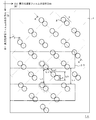
- FIG. 1A is an arrangement diagram of conductive particles in the anisotropic conductive film 1A of the example.
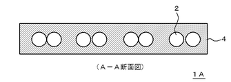
- FIG. 1B is an AA cross-sectional view of the anisotropic conductive film 1A of the example.
- FIG. 2A is a plan view of a mold used for manufacturing the anisotropic conductive film 1A of the example.
- FIG. 2B is a BB cross-sectional view of a mold used for manufacturing the anisotropic conductive film 1A of the example.
- FIG. 3 is an arrangement view of conductive particles in the anisotropic conductive film 1B of the example.
- FIG. 4 is an arrangement view of conductive particles in the anisotropic conductive film 1C of the example.
- FIG. 5 is an arrangement view of conductive particles in the anisotropic conductive film 1D of the example.
- FIG. 6 is an arrangement view of conductive particles in the anisotropic conductive film 1E of the example.
- FIG. 7 is an arrangement view of conductive particles in the anisotropic conductive film 1F of the example.
- FIG. 8 is an arrangement view of conductive particles in the anisotropic conductive film 1G of the example.
- FIG. 9 is an arrangement view of conductive particles in the anisotropic conductive film 1H of the example.
- FIG. 10 is an arrangement view of conductive particles in the anisotropic conductive film 1I of the example.
- FIG. 11 is an arrangement view of conductive particles in the anisotropic conductive film 1J of the example.
- FIG. 12 is an arrangement view of conductive particles in the anisotropic conductive film 1K of the example.
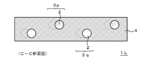
- FIG. 13A is an arrangement view of conductive particles in the anisotropic conductive film 1L of the example.
- FIG. 13B is a CC cross-sectional view of the anisotropic conductive film 1L of the example.
- FIG. 14A is an explanatory diagram of a method for producing the anisotropic conductive film 1L of the example.
- FIG. 14B is an explanatory diagram of a method for producing the anisotropic conductive film 1L of the example.
- FIG. 14C is an explanatory diagram of a method for producing the anisotropic conductive film 1L of the example.
- FIG. 14A is an explanatory diagram of a method for producing the anisotropic conductive film 1L of the example.
- FIG. 14B is an explanatory diagram of a method for producing the anisotropic conductive film 1L of the example.
- FIG. 14C is an
- FIG. 15A is an explanatory diagram of a preferred arrangement of the conductive particle units with respect to the connection terminals.
- FIG. 15B is an explanatory diagram of a preferred arrangement of the conductive particle units with respect to the connection terminals.
- FIG. 15C is an explanatory diagram of a preferred arrangement of the conductive particle units with respect to the connection terminals.
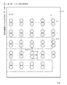
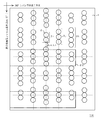
- FIG. 1A is an arrangement view of conductive particles 2 in an anisotropic conductive film 1A according to an embodiment of the present invention.
- anisotropic conductive film 1 ⁇ / b> A conductive particle units 3 in which two conductive particles 2 are arranged are arranged in a lattice pattern in the insulating adhesive layer 4. More specifically, the center of the conductive particle unit 3 is arranged at a lattice point of a square lattice indicated by a broken line.
- each conductive particle unit 3 the conductive particles 2 may be in contact with each other and may be close to each other with a gap therebetween, but the total size of the gaps in each conductive particle unit 3 (one conductive particle unit 3 Is composed of an array of n conductive particles, the sum of the sizes of n-1 gaps) increases the effect of the present invention that the conductive particle units are arranged in a lattice shape. It is preferably smaller than the particle diameter Le of the particles 2 and less than 1/4 of the particle diameter Le. Note that the total size of the gaps in the conductive particle unit 3 is larger when the angle ⁇ in the longitudinal direction of the conductive particle unit with respect to the longitudinal direction of the anisotropic conductive film is larger than when the angle ⁇ is small. As shown in FIG. 3 to be described later, when the angle ⁇ is 90 °, the effect of the present invention can be obtained even when the particle diameter Le of the conductive particles 2 is 1 ⁇ 2.
- the conductive particles 2 have the same particle diameter Le. Therefore, unless otherwise specified, in the present invention, the particle diameter Le of the conductive particles 2 means the average particle diameter of the conductive particles 2 constituting the anisotropic conductive film.
- each conductive particle unit 3 is aligned and is inclined with respect to the longitudinal direction D1 of the anisotropic conductive film 1A. More specifically, the angle ⁇ in the longitudinal direction of the conductive particle unit 3 with respect to the longitudinal direction of the anisotropic conductive film 1A is 45 °. Further, the longitudinal direction of each conductive particle unit 3 overlaps with a straight line (a straight line indicated by a broken line in the drawing) that forms a grid-like arrangement of the conductive particle units 3. Thus, when the longitudinal direction of the conductive particle unit 3 is inclined with respect to the longitudinal direction of the anisotropic conductive film 1A, the connection terminal 20 is connected when connecting the connection terminal of the electronic component using the anisotropic conductive film 1A. The number of trapped conductive particles 2 can be increased.
- FIG. 1B is an AA cross-sectional view of the anisotropic conductive film 1A cut along the longitudinal direction of the conductive particle unit 3. As shown in the figure, the conductive particles 2 are buried in the insulating adhesive layer 4 at a certain depth.
- the closest distance La between the conductive particles of adjacent conductive particle units 3 (adjacent conductive particles when a single conductive particle is also present at a lattice point, as will be described later).
- the closest distance La) between the conductive particles selected from the unit and single conductive particles increases the arrangement density of the conductive particles 2 in the anisotropic conductive film 1A as much as possible, and the first and first in the anisotropic conductive film 1A. From the point which prevents the short circuit between terminals at the time of anisotropic conductive connection of 2 electronic parts, it is 0.5 times or more of the particle diameter of conductive particles 2.
- the closest distance La is 0.5 times or more the particle diameter of the conductive particles 2 for the following reason. That is, when the first and second electronic components are anisotropically conductively connected using the anisotropic conductive film 1A, the conductive particles 2 are crushed between the connection terminals of the first and second electronic components facing each other. As indicated by the broken-line circle, the particle diameter of the conductive particles 2 is 1.2 to 1.3 times the particle diameter before connection. Therefore, even if the conductive particles of adjacent conductive particle units 3 that are at the closest distance are both crushed at the time of anisotropic conductive connection, at least about 1 ⁇ 4 of the particle diameter is between them. In order to ensure that there is a gap and prevent occurrence of a short circuit, the closest distance La between adjacent conductive particle units is set to 0.5 times or more of the particle diameter.
- the length La1 in the longitudinal direction D1 of the anisotropic conductive film having the closest distance La is preferably 10 times or less the particle diameter Le of the conductive particles 2. This is because setting the number density of the conductive particles to a certain value or more leads to stable capture of the conductive particles at the connection terminal 20 and contributes to the stability of the fine pitch connection.
- the circumscribing line in the longitudinal direction D1 of the anisotropic conductive film of the conductive particle unit 3 overlaps the adjacent conductive particle unit 3 in the same direction D1 (external tangent line). Penetrating the conductive particles of adjacent units) is preferable because it contributes to the stability of the connection at a fine pitch by increasing the number density of the conductive particles.
- the direction of the closest distance La is the longitudinal direction of the conductive particle unit 3.
- the direction of the closest distance La is the conductive particle unit 3. It is not restricted to the longitudinal direction.
- the longitudinal direction D1 of the anisotropic conductive film 1A is shown in FIG. It is preferable to match with the arrangement direction of the connection terminals 20 indicated by the two-dot chain line (the short direction of the connection terminals 20). In other words, the short direction D2 of the anisotropic conductive film 1A is matched with the longitudinal direction of the connection terminal 20.
- the length Lb in the longitudinal direction D1 of the anisotropic conductive film 1A of each conductive particle unit 3 the distance Lx between the connection terminals 20 connected by the anisotropic conductive film 1A, and the particle diameter Le of the conductive particles.
- the conductive particle 2 of the adjacent conductive particle unit 3 is the closest conductive particle that overlaps in the longitudinal direction D1 of the anisotropic conductive film 1A (that is, the conductive particle 2 is projected in the longitudinal direction of the anisotropic conductive film 1A.
- the distance Lc in the longitudinal direction D1 between the conductive particles having the projected images overlapped with each other be 0.5 times or more the particle diameter of the conductive particles. That is, the distance Lc changes according to the angle ⁇ of the conductive particle unit 3 in the longitudinal direction with respect to the longitudinal direction D1 of the anisotropic conductive film 1A even if the grid-like arrangement of the conductive particle units 3 is the same. Therefore, in order to prevent a short circuit between the adjacent connection terminals 20 regardless of the size of the angle ⁇ , it is preferable to secure 0.5 times or more the particle diameter of the conductive particles as the distance Lc.
- the particle diameter of the conductive particles 2 is preferably 1 to 10 ⁇ m, more preferably 2 to 4 ⁇ m, from the viewpoint of short circuit prevention and connection stability between the connection terminals.
- the arrangement density of the conductive particles 2 is preferably 2000 to 250,000 pieces / mm 2 , more preferably 4000 to 100,000 pieces / mm 2 .
- the arrangement density of the conductive particles is appropriately adjusted depending on the number of the conductive particles 2 constituting the conductive particle unit 3 and the arrangement of the conductive particle units 3.
- the configuration of the conductive particles 2 itself, the layer configuration of the insulating adhesive layer 4 or the constituent resin is not particularly limited. That is, as the conductive particles 2, those used in known anisotropic conductive films can be appropriately selected and used. Examples thereof include metal particles such as nickel, cobalt, silver, copper, gold, and palladium, and metal-coated resin particles. Two or more kinds can be used in combination.
- an insulating resin layer used in a known anisotropic conductive film can be appropriately adopted.
- a photo radical polymerization type resin layer containing an acrylate compound and a photo radical polymerization initiator a heat radical polymerization type resin layer containing an acrylate compound and a heat radical polymerization initiator, a heat containing an epoxy compound and a heat cationic polymerization initiator
- a cationic polymerization type resin layer, a thermal anion polymerization type resin layer containing an epoxy compound and a thermal anion polymerization initiator, or the like can be used.
- these resin layers can be polymerized as necessary.
- the insulating adhesive layer 4 may be formed from a plurality of resin layers.
- an insulating filler such as silica fine particles, alumina, or aluminum hydroxide may be added to the insulating adhesive layer 4 as necessary.
- the blending amount of the insulating filler is preferably 3 to 40 parts by mass with respect to 100 parts by mass of the resin forming the insulating adhesive layer.
- a mold having a dent corresponding to the arrangement of the conductive particle unit 3 is machined, laser processed, photo Prepared by a known method such as lithography, put conductive particles in the mold, fill the composition for forming an insulating adhesive layer thereon, cure, take out from the mold, and further provide an insulating adhesive layer if necessary What is necessary is just to laminate.
- type which puts the electrically-conductive particle 2 a mold
- the length Li of the recess 11 in the longitudinal direction depends on the number of conductive particles 2 filled in the recess 11, but the longitudinal direction of the recess 11 in the gaps s 1, s 2, s 3 after the recess 11 is filled with the conductive particles 2. It is preferable that the total length Lj be less than 1 ⁇ 4 of the particle diameter of the conductive particles 2.
- the conductive particle units are arranged in a grid, the conductive particles are arranged in a grid as a conductive particle unit without the conductive particles forming a unit. This is to make it possible to clearly distinguish the states arranged in a lattice pattern.
- a member having through holes formed in a predetermined arrangement is provided on the insulating adhesive layer-forming composition layer.
- the conductive particles 2 may be supplied from the through holes and passed through the through holes.
- the anisotropic conductive film of the present invention can take various forms.
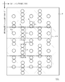
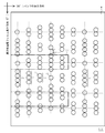
- the anisotropic conductive film 1B shown in FIG. 3 and the anisotropic conductive film 1C shown in FIG. 4 are arranged in the same manner as the anisotropic conductive film 1A shown in FIG.
- the conductive particle unit 3 is formed of two conductive particles 2, and the conductive particle units 3 are aligned in the longitudinal direction, and the conductive particle units 3 are arranged in a square lattice pattern.
- the angle ⁇ in the longitudinal direction of the conductive particle unit 3 with respect to the longitudinal direction of the anisotropic conductive film 1B is 90 °.
- the angle ⁇ in the longitudinal direction of the conductive particle unit 3 with respect to the longitudinal direction of the film 1C is 0 °.
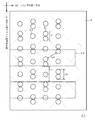
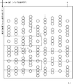
- the anisotropic conductive film 1D shown in FIG. 5 has the conductive particle unit 3 arranged so that the center point of the conductive particle unit 3 forms a hexagonal lattice in the anisotropic conductive film 1A shown in FIG. 1A.
- the angle ⁇ of the longitudinal direction of the conductive particle unit 3 with respect to the longitudinal direction of the anisotropic conductive film 1D is set to 30 °.
- the grid-like arrangement of the conductive particle units 3 can take various forms.
- the conductive particle units 3 may be arranged in an oblique lattice shape, a rectangular lattice shape, or the like.
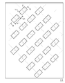
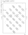
- An anisotropic conductive film 1E shown in FIG. 6 is formed by forming each conductive particle unit 3 from three conductive particles 2 arranged in a line, and arranging each conductive particle unit 3 in an oblique array.
- the angle ⁇ in the longitudinal direction of each conductive particle unit 3 with respect to the longitudinal direction of the conductive conductive film 1E is set to 45 °.
- the number of the conductive particles 2 constituting the conductive particle unit 3 is not limited to two, and can be determined according to the conductive particle diameter, the distance between terminals to be connected, the size and layout of the terminals, etc., so there is no upper limit. . This is because even if the fine pitch and the area are reduced, the risk of occurrence of a short circuit is reduced if there is a sufficient distance between terminals according to the conductive particle diameter.
- the number of conductive particles 2 constituting one conductive particle unit 3 can be 2 to 8, more preferably 2 to 5.
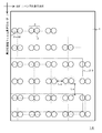
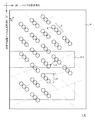
- a plurality of conductive particle units 3i and 3k having different numbers of conductive particles forming conductive particle units are arranged in a lattice shape, and a single conductive material other than the lattice points is provided. You may arrange
- a plurality of conductive particle units 3i and 3k having different numbers of conductive particles forming the conductive particle unit are arranged in a lattice shape, the centers of the respective conductive particle units 3i and 3k may be arranged at a lattice point.
- each of the conductive particle units 3i, 3j, 3k is arranged like an anisotropic conductive film 1H shown in FIG.
- the number of conductive particles of the conductive particle units arranged in the longitudinal direction and arranged in the short direction may be gradually increased or decreased.
- the longitudinal direction of the three conductive particle units 3i, 3j, and 3k is the longitudinal direction of the anisotropic conductive film 1H, but the longitudinal directions of the conductive particle units 3i, 3j, and 3k are aligned. If so, the longitudinal direction can be set to an arbitrary direction.
- the conductive particle unit and the single conductive particle may be arranged in a lattice shape.
- single conductive particles may exist at lattice points.
- three conductive particle units 3i, 3j, and 3k having different numbers of conductive particles forming conductive particle units and single conductive particles 2a are arranged in a lattice shape.
- the closest distance La between the conductive particles selected from the conductive particle units 3i, 3j, 3k and the single conductive particle 2a is set to 0.5 times or more the conductive particle diameter of the conductive particles 2, 2a.
- connection terminal Even when an anisotropic conductive film is attached, even if the attachment position of the film is slightly shifted in the longitudinal direction of the connection terminal (several tens of ⁇ m or more of the film width), it is captured by the connection terminal. This is preferable because the variation in the number of conductive particles is small, and the variation in the pressing force applied to the conductive particles between when there is no positional deviation and when there is no positional deviation is preferable.
- the size of the connection surface is 4 to 60 ⁇ m wide and the length is 400 ⁇ m or less (the lower limit is equal to the width), or the width of the connection surface is 4 of the conductive particle diameter.
- the conductive particle unit 3 is less than twice the length in the longitudinal direction, and the minimum distance between the connection terminals is, for example, 8 to 30 ⁇ m. Further, since the distance between the connection terminals may be relatively large when the area of the connection terminal is small, the distance between the terminals is not limited to the above-described distance.
- reducing the terminal area has a merit in terms of cost because it reduces the metal (Au, etc.) used as a terminal, in addition to technical reasons such as high integration, and can accommodate a small terminal area.
- the significance of the anisotropic conductive film is great.
- the conductive particles are arranged in a line in each conductive particle unit 3 in order to improve the trapping property of the conductive particles at the fine pitch.
- the conductive particles 2 in the conductive particle unit 3 are arranged in the first direction and the second direction which are different from each other. Can be made compatible.
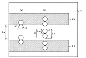
- a first mold 10p and a second conductive particle unit for arranging conductive particles in the first conductive particle unit 3p As a method for producing such an anisotropic conductive film 1L, for example, as shown in FIG. 14A, a first mold 10p and a second conductive particle unit for arranging conductive particles in the first conductive particle unit 3p.
- the second mold 10q for arranging the conductive particles in 3q is used to fill the recesses 11 of the respective molds 10p, 10q with the conductive particles 2, and as shown in FIG. 14B, the respective molds 10p, 10q
- the insulating adhesive layer forming composition layer 5 formed on the release sheet 6 is placed, and the insulating adhesive layer forming composition layer 5 is pushed into the recesses 11 of the molds 10p and 10q, and dried, heated, etc.
- the arrangement pitch of the recesses 11 in each mold can be increased compared to the case of using a single mold.
- the productivity of the anisotropic conductive film 1L can be improved.
- the anisotropic conductive film of the present invention includes a connection terminal of a first electronic component such as an IC chip, an IC module, or an FPC, and a connection terminal of a second electronic component such as an FPC, a glass substrate, a plastic substrate, a rigid substrate, or a ceramic substrate. Can be preferably used in anisotropic conductive connection.
- the connection structure thus obtained is also part of the present invention.
- the first electronic components can be anisotropically conductively connected by stacking IC chips or IC modules.
- the connection structure thus obtained is also part of the present invention.
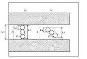
- the conductive particle 2 constituting the conductive particle unit 3 is attached to the edge of the connection terminal 20 as shown in FIG. Although it is preferable to connect at a position where it does not rest, as shown in FIG.
- the inter-terminal distance Lx of the connection terminal 20 the length Ld of the conductive particle unit 3 in the direction of the inter-terminal distance
- the relationship between the particle diameter Le of the particles 2 is Lx> (Ld + Le)
- the length Ld of the conductive particle unit 3 and the particle diameter Le of the conductive particles 2 in the direction of the inter-terminal distance Lx may be adjusted with respect to the inter-terminal distance Lx of the connection terminals 20 so as to satisfy the above.
- the above equation may be satisfied by reducing the particle diameter Le of the conductive particles 2.
- Examples 1 to 11 and Comparative Examples 1 and 2 ⁇ Outline of manufacturing anisotropic conductive film>
- the central arrangement of the conductive particle units forms a rectangular lattice, and the number of conductive particles per conductive particle unit (hereinafter referred to as the number of connected particles), the particle diameter of the conductive particles ( ⁇ m), the maximum length of the conductive particle unit ( ⁇ m), the angle ⁇ of the longitudinal direction of the conductive particle unit with respect to the longitudinal direction of the anisotropic conductive film, the closest distance La ( ⁇ m) between the conductive particles of adjacent conductive particle units, and the arrangement density of conductive particles (pieces / mm 2 ) Produced anisotropic conductive films having the numerical values shown in Table 1.
- conductive particles particles (particle diameter 2 ⁇ m, 3 ⁇ m or 6 ⁇ m) prepared as follows were used as the conductive particles.
- ⁇ Preparation of conductive particles (particle diameter 2 ⁇ m, 3 ⁇ m or 6 ⁇ m)> Benzoyl peroxide was added as a polymerization initiator to a solution adjusted for the mixing ratio of divinylbenzene, styrene, and butyl methacrylate, and the mixture was heated with uniform stirring at high speed to perform a polymerization reaction, thereby obtaining a fine particle dispersion. The fine particle dispersion was filtered and dried under reduced pressure to obtain a block body that was an aggregate of fine particles. Further, the block bodies were pulverized and classified to obtain divinylbenzene resin particles having an average particle size of 2 ⁇ m, 3 ⁇ m and 6 ⁇ m.
- the palladium catalyst was supported on the divinylbenzene resin particles (5 g) thus obtained by an immersion method.
- an electroless nickel plating solution pH 12, plating solution temperature 50 ° C.
- nickel sulfate hexahydrate, sodium hypophosphite, sodium citrate, triethanolamine and thallium nitrate is applied to the resin particles.
- Electroless nickel plating was used to obtain nickel-coated resin particles having a nickel plating layer (metal layer) formed on the surface as conductive particles.
- the average particle diameter of the obtained conductive particles was 2 ⁇ m, 3 ⁇ m and 6 ⁇ m.
- An aqueous suspension was prepared by mixing 12 g of the above-mentioned nickel-coated resin particles in a solution obtained by dissolving 10 g of sodium chloroaurate in 1000 mL of ion-exchanged water.
- a gold plating bath was prepared by adding 15 g of ammonium thiosulfate, 80 g of ammonium sulfite, and 40 g of ammonium hydrogen phosphate to the obtained aqueous suspension. After adding 4 g of hydroxylamine to the obtained gold plating bath, the pH of the gold plating bath is adjusted to 9 using ammonia, and the bath temperature is maintained at 60 ° C. for about 15 to 20 minutes, so that the average particle diameter is 2 ⁇ m, 3 ⁇ m. And 6 ⁇ m gold / nickel-coated resin particles were obtained and used as conductive particles.
- An anisotropic conductive film in which the conductive particles are contained in the insulating adhesive layer in the arrangement shown in Table 1 was produced as follows. First, 60 parts by mass of phenoxy resin (Nippon Steel & Sumikin Chemical Co., Ltd., YP-50), 40 parts by mass of epoxy resin (Mitsubishi Chemical Corporation, jER828), cationic polymerization initiator (latent curing agent) (Sanshin Chemical Industry Co., Ltd.) (Co., Ltd., SI-60L) A heat-polymerizable insulating resin composition containing 2 parts by mass was prepared, applied onto a PET film having a film thickness of 50 ⁇ m, and dried in an oven at 80 ° C. for 5 minutes. An adhesive layer having a thickness of 20 ⁇ m was formed on the PET film.
- a mold in which the arrangement of the protrusions is the arrangement of the conductive particle units shown in Table 1 is prepared, and the pellets of the transparent resin are melted, poured into the mold, cooled, and hardened to form the depressions in Table 1.
- a resin mold to be the arrangement of the conductive particle unit is prepared, and the resin mold is filled with the conductive particles, and the above-mentioned adhesive layer is covered thereon, the adhesive layer is cured by irradiation with ultraviolet rays, and peeled off from the mold. A conductive film was produced.
- (a) Conduction resistance The conduction resistances of three types of connection objects for evaluation having different effective connection areas (areas where the bump and the substrate face each other) were connected.
- the anisotropic conductive films of each Example and Comparative Example were sandwiched between a conductive resistance evaluation IC and a glass substrate, and heated and pressurized (180 ° C., 80 MPa, 5 seconds) to obtain each evaluation connection,
- the conduction resistance of the connection object for evaluation was measured by a value when a current of 2 mA was applied by a four-terminal method using a digital multimeter. If it is less than 1 ⁇ , there is no practical problem.
- each IC for evaluation and the glass substrate correspond to their terminal patterns, and the sizes are as follows.
- the longitudinal direction of the anisotropic conductive film was match
- the bump specifications of the conductive resistance evaluation IC are changed to the following, the alignment of the evaluation IC is intentionally shifted by 6 ⁇ m and 8 ⁇ m in the short (width) direction of the bump, and the effective connection area is set to 300 ⁇ m 2 or 200 ⁇ m 2 . Except for the above, connection was made in the same manner as in (a-1) to obtain an evaluation connection, and the conduction resistance was measured in the same manner as in (a-1). The results are shown in Table 1B. Table 1B shows numerical values of substantial bump sizes and IC bump-bump spaces (that is, horizontal conductor distances between bumps of the same IC). Bump specifications Gold plating, height 12 ⁇ m, size 12 ⁇ 50 ⁇ m, distance between bumps 10 ⁇ m
- connection object for evaluation 100 bumps each was obtained, and in the same manner as described above, the minimum number of particles captured in each bump was determined. It was evaluated with. If it is more than C evaluation, there is no practical problem.
- evaluation criteria A (very good): 10 or more B (good): 5 or more, less than 10 C (normal): 3 or more, less than 5 D (defect): less than 3
- the conduction resistance is 0.4 to 0.6 ⁇ when the closest distance La of the conductive particle unit is in the range of 0.5 to 3 times the particle diameter of the conductive particles.
- the conduction resistance is as high as 0.8 ⁇ , and short-circuits occur relatively frequently. I understand that.
- Comparative Example 2 it can be seen from Comparative Example 2 that the number of shorts is significantly increased when the closest distance La of the conductive particle unit is less than 0.5 times the particle diameter of the conductive particles.
- Comparative Example 1 and Comparative Example 2 it can be seen from the particle state between the bumps that the particle diameter of the conductive particles is too large with respect to the distance between the bumps, and therefore is not compatible with the bump layout.
- Comparative Example 2 it can be seen that the minimum number of particles captured per bump is 0, the conductive particles are not captured by the bumps, and the anisotropic connection is not stable. Thereby, it turns out that it cannot respond to the anisotropic connection in a fine pitch only by enlarging the occupation area rate of an electrically-conductive particle by enlarging the particle diameter of an electrically-conductive particle.
- the number of conductive particles connected in the conductive particle unit is not particularly limited in the short direction of the anisotropic conductive film (longitudinal direction of the bump) (Reference Examples 1 and 2).
- the direction it can be seen that the number of shorts increases when the sum of the maximum length of the conductive particle unit and the diameter of the conductive particle is larger than the distance between the bumps (Reference Examples 3 to 5). Therefore, even when using the anisotropic conductive film of an Example, it turns out that it is preferable to adjust the direction of an anisotropic conductive film according to the maximum length of an electroconductive particle unit and the distance between terminals of a connection terminal.
Abstract
Description
Lx>(Lb+Le)
Lx>(Ld+Le)
を満たすように接続端子20の端子間距離Lxに対し、該端子間距離Lxの方向の導電粒子ユニット3の長さLdと導電粒子2の粒子径Leを調整すればよい。
Lx>(Ld+Le)
が満たされないと接続端子20間でショートが発生し易くなる。しかしながら、導電粒子ユニット3を構成する導電粒子2の粒子径Leや導電粒子2の配列数が等しくても、同図(b)に示すように、端子間距離Lxの方向に対して導電粒子ユニット3の長手方向を傾け、端子間距離Lxの方向の導電粒子ユニット3の長さLdを短くし、上述の式が満たされるようにすればよい。
実施例1~11及び比較例1、2
<異方導性導電フィルムの製造の概要>
導電粒子ユニットの中心の配列が長方格子を形成し、一つの導電粒子ユニットあたりの導電粒子の個数(以下、連結個数という)、導電粒子の粒子径(μm)、導電粒子ユニットの最大長(μm)、異方性導電フィルムの長手方向に対する導電粒子ユニットの長手方向の角度θ、隣接する導電粒子ユニットの導電粒子同士の最近接距離La(μm)、導電粒子の配置密度(個/mm2)が表1に示す数値の異方性導電フィルムを製造した。
ジビニルベンゼン、スチレン、ブチルメタクリレートの混合比を調整した溶液に、重合開始剤としてベンゾイルパーオキサイドを投入して高速で均一攪拌しながら加熱を行い、重合反応を行うことにより微粒子分散液を得た。前記微粒子分散液をろ過し減圧乾燥することにより微粒子の凝集体であるブロック体を得た。更に、前記ブロック体を粉砕し分級することにより、平均粒子径2μm、3μmおよび6μmのジビニルベンゼン系樹脂粒子を得た。
この導電粒子が絶縁接着剤層中に表1の配列で含まれている異方性導電フィルムを次のようにして製造した。まず、フェノキシ樹脂(新日鉄住金化学(株)、YP-50)60質量部、エポキシ樹脂(三菱化学(株)、jER828)40質量部、カチオン重合開始剤(潜在性硬化剤)(三新化学工業(株)、SI-60L)2質量部を含有する熱重合性の絶縁性樹脂組成物を調製し、これをフィルム厚さ50μmのPETフィルム上に塗布し、80℃のオーブンにて5分間乾燥させ、PETフィルム上に厚み20μmの粘着層を形成した。
(a)導通抵抗、(b)ショート数、(c)バンプ1個当たりの粒子最小捕捉数、(d)バンプ間の粒子状態を次のように評価した。結果を表1A及び表1Bに示す。
有効接続面積(バンプと基板とが対峙する面積)が異なる3通りの評価用接続物の導通抵抗を接続した。
(a-1)導通抵抗(有効接続面積400μm2)
各実施例及び比較例の異方性導電フィルムを、導通抵抗評価用ICとガラス基板の間に挟み、加熱加圧(180℃、80MPa、5秒)して各評価用接続物を得、この評価用接続物の導通抵抗はデジタルマルチメータを用いて4端子法で2mAの電流を通電したときの値で測定した。1Ω未満であれば、実用上問題はない。
ここで、この各評価用ICとガラス基板は、それらの端子パターンが対応しており、サイズは次の通りである。
また、異方性導電フィルムを用いて評価用ICとガラス基板を接続する場合、異方性導電フィルムの長手方向をバンプの短手方向(端子間距離の方向)に合わせた。結果を表1Aに示す。
外径 0.7×20mm
厚み 0.2mm
バンプ仕様 金メッキ、高さ12μm、サイズ10×40μm、バンプ間距離10μm
ガラス材質 コーニング社製
外径 30×50mm
厚み 0.5mm
電極 ITO配線
導通抵抗評価用ICのバンプ仕様を以下のものに変更し、評価用ICのアライメントをバンプの短手(幅)方向に6μmおよび8μm意図的にずらし、有効接続面積を300μm2又は200μm2とする以外は、(a-1)と同様にして接続して評価用接続物を得、その導通抵抗を(a-1)と同様に測定した。結果を表1Bに示す。なお、表1Bには、実質的なバンプの大きさとICのバンプ-バンプ間スペース(即ち、同一ICのバンプ間での水平方向の導体距離)の数値を示した。
バンプ仕様 金メッキ、高さ12μm、サイズ12×50μm、バンプ間距離10μm
実施例1~11及び比較例1~2の導通抵抗評価用接続物のバンプ間100個においてショートしているチャンネル数を計測し、ショート数とした。
櫛歯TEG(test element group))
外径 1.5×13mm
厚み 0.5mm
バンプ仕様 金メッキ、高さ15μm、サイズ25×140μm、バンプ間距離7.5μm
各実施例及び比較例の異方性導電フィルムを用いて、(a-1)と同様にして評価用接続物(バンプ100個)を得、各バンプにおける粒子捕捉数を計測し、その最小数を求めた。なお、この接続においても、異方性導電フィルムの長手方向をバンプの短手方向(端子間距離の方向)に合わせた。結果を表1Aに示す。
(評価基準)
A(非常に良好):10個以上
B(良好):5個以上、10個未満
C(普通):3個以上、5個未満
D(不良):3個未満
(c)の評価用接続物(即ち、(a-1)、(a-2)、(a-3)と同様にして得た評価用接続物)において、バンプ-バンプ間においてバンプと接続していない導電粒子が互いに連結することにより形成された導電粒子群の発生数をカウントした。表1Aに、(a-1)と同様にして得た評価用接続物について、バンプ-バンプ間の個数100あたりの、接続前の状態に対して導電粒子ユニットもしくは導電粒子が連結した導電粒子群のカウント値を示す。このカウント値により、異方性導電接続における導電粒子の移動のし易さ(即ち、導電粒子の接触によるショートの発生リスク)を評価することができる。


表2に示す導電粒子の連結個数と配置とし、実施例1と同様にして異方性導電フィルムを製造し、評価した。結果を表2に示す。

表3に示す導電粒子の連結個数の配置とし、実施例1と同様にして異方性導電フィルムを製造し、評価した。結果を表3に示す。
表3から、導電粒子ユニットの長手方向と異方性導電フィルムの短手方向(接続端子の長手方向)とが揃っている場合、個々の導電粒子ユニット内の導電粒子の間隙をゼロから導電粒子の粒子径の1/2の大きさまで任意に変更しても導電粒子ユニットが格子状に配列した状態を形成することができ、ショート数を低減し導通信頼性を高められることがわかる。

2、2a 導電粒子
3、3a、3b、3p、3q、3i、3j、3k 導電粒子ユニット
4 絶縁接着剤層
5 絶縁接着剤層形成用組成物層
6 剥離シート
10、10p、10q 型
11 凹み
20 接続端子
D1 異方性導電フィルムの長手方向
D2 異方性導電フィルムの短手方向
La 隣接する導電粒子ユニット及び単独の導電粒子から選ばれる導電粒子同士の最近接距離
La1 隣接する導電粒子ユニットの最近接距離の異方性導電フィルムの長手方向の長さ
Lb 導電粒子ユニットの異方性導電フィルムの長手方向の長さ
Lc 隣接する導電粒子ユニットの導電粒子であって、異方性導電フィルムの長手方向で重なる最近接導電粒子同士の該長手方向の距離
Ld 接続端子間距離の方向の導電粒子ユニットの長さ
Le 導電粒子の粒子径
Lh 型の凹みの長手方向に隣接する凹み同士の距離
Li 型の凹みの、該凹みの長手方向の長さ
Lj 型の凹みに導電粒子を充填した後の間隙の、該凹みの長手方向の長さの合計
Lx 接続端子間距離
s1、s2、s3 間隙
θ 異方性導電フィルムの長手方向に対する導電粒子ユニットの長手方向の角度
Claims (7)
- 導電粒子が一列に配列した導電粒子ユニット、又は導電粒子が一列に配列した導電粒子ユニットと単独の導電粒子が、絶縁接着剤層中に格子状に配置された異方性導電フィルムであって、隣接する導電粒子ユニット及び単独の導電粒子から選ばれる導電粒子同士の最近接距離が導電粒子の粒子径の0.5倍以上である異方性導電フィルム
- 隣接する導電粒子ユニットの導電粒子であって、異方性導電フィルムの長手方向で重なる最近接導電粒子同士の該長手方向の距離が、導電粒子の粒子径の0.5倍以上である請求項1記載の異方性導電フィルム。
- 各導電粒子ユニットの長手方向が、異方性導電フィルムの長手方向に対して傾いている請求項1又は2に記載の異方性導電フィルム。
- 導電粒子ユニットを形成する導電粒子数が異なる複数通りの導電粒子ユニットが配置されている請求項1~3いずれかに記載の異方性導電フィルム。
- 導電粒子ユニットとして、該ユニットにおける導電粒子の配列方向が第1の方向の導電粒子ユニットと、第2の方向の導電粒子ユニットを有する請求項1~4のいずれかに記載の異方性導電フィルム。
- 請求項1~5のいずれかに記載の異方性導電フィルムを用いて第1電子部品の接続端子と第2電子部品の接続端子とを異方性導電接続した接続構造体。
- 接続端子間の距離が、該接続端子間の距離方向の導電粒子ユニットの長さと、導電粒子の粒子径との和よりも大きい請求項6記載の接続構造体。
Priority Applications (3)
| Application Number | Priority Date | Filing Date | Title |
|---|---|---|---|
| US15/517,781 US9953947B2 (en) | 2014-10-28 | 2015-10-28 | Anisotropic conductive film and connection structure |
| CN201580055635.4A CN106797082B (zh) | 2014-10-28 | 2015-10-28 | 各向异性导电膜及连接结构体 |
| KR1020177006076A KR101937601B1 (ko) | 2014-10-28 | 2015-10-28 | 이방성 도전 필름 및 접속 구조체 |
Applications Claiming Priority (2)
| Application Number | Priority Date | Filing Date | Title |
|---|---|---|---|
| JP2014219788 | 2014-10-28 | ||
| JP2014-219788 | 2014-10-28 |
Publications (1)
| Publication Number | Publication Date |
|---|---|
| WO2016068169A1 true WO2016068169A1 (ja) | 2016-05-06 |
Family
ID=55857504
Family Applications (1)
| Application Number | Title | Priority Date | Filing Date |
|---|---|---|---|
| PCT/JP2015/080338 WO2016068169A1 (ja) | 2014-10-28 | 2015-10-28 | 異方性導電フィルム及び接続構造体 |
Country Status (6)
| Country | Link |
|---|---|
| US (1) | US9953947B2 (ja) |
| JP (1) | JP6661969B2 (ja) |
| KR (1) | KR101937601B1 (ja) |
| CN (1) | CN106797082B (ja) |
| TW (1) | TWI648913B (ja) |
| WO (1) | WO2016068169A1 (ja) |
Families Citing this family (14)
| Publication number | Priority date | Publication date | Assignee | Title |
|---|---|---|---|---|
| TWI613684B (zh) * | 2012-08-01 | 2018-02-01 | Dexerials Corp | 異向性導電膜之製造方法、異向性導電膜、及連接結構體 |
| CN104541417B (zh) * | 2012-08-29 | 2017-09-26 | 迪睿合电子材料有限公司 | 各向异性导电膜及其制备方法 |
| TWI732746B (zh) | 2014-11-17 | 2021-07-11 | 日商迪睿合股份有限公司 | 異向性導電膜之製造方法 |
| JP7274811B2 (ja) | 2016-05-05 | 2023-05-17 | デクセリアルズ株式会社 | 異方性導電フィルム |
| WO2017191772A1 (ja) * | 2016-05-05 | 2017-11-09 | デクセリアルズ株式会社 | フィラー配置フィルム |
| CN113707361B (zh) * | 2016-05-05 | 2023-08-22 | 迪睿合株式会社 | 各向异性导电膜 |
| US20170338204A1 (en) * | 2016-05-17 | 2017-11-23 | Taiwan Semiconductor Manufacturing Company, Ltd. | Device and Method for UBM/RDL Routing |
| JP7077963B2 (ja) * | 2017-01-27 | 2022-05-31 | 昭和電工マテリアルズ株式会社 | 絶縁被覆導電粒子、異方導電フィルム、異方導電フィルムの製造方法、接続構造体及び接続構造体の製造方法 |
| JP2019029135A (ja) * | 2017-07-27 | 2019-02-21 | 日立化成株式会社 | 異方性導電フィルム及びその製造方法、並びに接続構造体及びその製造方法 |
| KR102519126B1 (ko) * | 2018-03-30 | 2023-04-06 | 삼성디스플레이 주식회사 | 표시 장치 |
| TWI826476B (zh) * | 2018-06-26 | 2023-12-21 | 日商力森諾科股份有限公司 | 各向異性導電膜及其製造方法以及連接結構體的製造方法 |
| US20200156291A1 (en) * | 2018-11-21 | 2020-05-21 | Shin-Etsu Chemical Co., Ltd. | Anisotropic film and method for manufacturing anisotropic film |
| TW202130748A (zh) * | 2019-10-15 | 2021-08-16 | 國立大學法人京都大學 | 導電膜、分散體及其等之製造方法、以及含導電膜之裝置 |
| JPWO2021193911A1 (ja) * | 2020-03-26 | 2021-09-30 |
Citations (5)
| Publication number | Priority date | Publication date | Assignee | Title |
|---|---|---|---|---|
| JPH0582199A (ja) * | 1991-05-28 | 1993-04-02 | Minato Electron Kk | 異方導電性コネクタを有するコネクタ配置構造および異方導電性コネクタ |
| JPH09320345A (ja) * | 1996-05-31 | 1997-12-12 | Whitaker Corp:The | 異方導電性フィルム |
| JP2002519473A (ja) * | 1998-06-30 | 2002-07-02 | ミネソタ マイニング アンド マニュファクチャリング カンパニー | ファインピッチの異方導電性接着剤 |
| JP2006049783A (ja) * | 2004-06-29 | 2006-02-16 | Yuji Suda | 異方性導電接着フィルムの製造方法と電極接続方法 |
| JP2007165052A (ja) * | 2005-12-12 | 2007-06-28 | Sumitomo Bakelite Co Ltd | 異方導電性フィルム |
Family Cites Families (10)
| Publication number | Priority date | Publication date | Assignee | Title |
|---|---|---|---|---|
| US5502889A (en) * | 1988-06-10 | 1996-04-02 | Sheldahl, Inc. | Method for electrically and mechanically connecting at least two conductive layers |
| US20070212521A1 (en) * | 2004-03-30 | 2007-09-13 | Tokai Rubber Industries, Ltd. | Anisotropic Conductive Film and a Method of Manufacturing the Same |
| JP4887700B2 (ja) * | 2005-09-09 | 2012-02-29 | 住友ベークライト株式会社 | 異方導電性フィルムおよび電子・電機機器 |
| JP5145110B2 (ja) * | 2007-12-10 | 2013-02-13 | 富士フイルム株式会社 | 異方導電性接合パッケージの製造方法 |
| JP5226562B2 (ja) * | 2008-03-27 | 2013-07-03 | デクセリアルズ株式会社 | 異方性導電フィルム、並びに、接合体及びその製造方法 |
| JP5049176B2 (ja) * | 2008-03-27 | 2012-10-17 | ソニーケミカル&インフォメーションデバイス株式会社 | 接合体及びその製造方法、並びに、異方性導電材料及びその製造方法 |
| KR20120036721A (ko) * | 2010-10-08 | 2012-04-18 | 제일모직주식회사 | 이방성 도전 필름 |
| JP6245792B2 (ja) | 2012-03-29 | 2017-12-13 | デクセリアルズ株式会社 | 導電性粒子、回路接続材料、実装体、及び実装体の製造方法 |
| JP6056700B2 (ja) * | 2012-08-03 | 2017-01-11 | デクセリアルズ株式会社 | 異方性導電フィルム及びその製造方法 |
| KR102520294B1 (ko) * | 2014-10-31 | 2023-04-10 | 데쿠세리아루즈 가부시키가이샤 | 이방성 도전 필름 |
-
2015
- 2015-10-27 JP JP2015211174A patent/JP6661969B2/ja active Active
- 2015-10-28 WO PCT/JP2015/080338 patent/WO2016068169A1/ja active Application Filing
- 2015-10-28 KR KR1020177006076A patent/KR101937601B1/ko active IP Right Grant
- 2015-10-28 TW TW104135558A patent/TWI648913B/zh active
- 2015-10-28 CN CN201580055635.4A patent/CN106797082B/zh active Active
- 2015-10-28 US US15/517,781 patent/US9953947B2/en active Active
Patent Citations (5)
| Publication number | Priority date | Publication date | Assignee | Title |
|---|---|---|---|---|
| JPH0582199A (ja) * | 1991-05-28 | 1993-04-02 | Minato Electron Kk | 異方導電性コネクタを有するコネクタ配置構造および異方導電性コネクタ |
| JPH09320345A (ja) * | 1996-05-31 | 1997-12-12 | Whitaker Corp:The | 異方導電性フィルム |
| JP2002519473A (ja) * | 1998-06-30 | 2002-07-02 | ミネソタ マイニング アンド マニュファクチャリング カンパニー | ファインピッチの異方導電性接着剤 |
| JP2006049783A (ja) * | 2004-06-29 | 2006-02-16 | Yuji Suda | 異方性導電接着フィルムの製造方法と電極接続方法 |
| JP2007165052A (ja) * | 2005-12-12 | 2007-06-28 | Sumitomo Bakelite Co Ltd | 異方導電性フィルム |
Also Published As
| Publication number | Publication date |
|---|---|
| TW201637290A (zh) | 2016-10-16 |
| US20170309590A1 (en) | 2017-10-26 |
| JP2016085983A (ja) | 2016-05-19 |
| KR101937601B1 (ko) | 2019-01-10 |
| US9953947B2 (en) | 2018-04-24 |
| TWI648913B (zh) | 2019-01-21 |
| JP6661969B2 (ja) | 2020-03-11 |
| KR20170039284A (ko) | 2017-04-10 |
| CN106797082A (zh) | 2017-05-31 |
| CN106797082B (zh) | 2019-07-30 |
Similar Documents
| Publication | Publication Date | Title |
|---|---|---|
| WO2016068169A1 (ja) | 異方性導電フィルム及び接続構造体 | |
| JP6504307B1 (ja) | 異方導電性フィルム | |
| JP6380591B2 (ja) | 異方導電性フィルム及び接続構造体 | |
| JP7176550B2 (ja) | 異方導電性フィルム及び接続構造体 | |
| WO2015141830A1 (ja) | 異方性導電フィルム及びその製造方法 | |
| CN107112314B (zh) | 多层基板 | |
| CN110499119B (zh) | 各向异性导电性膜及连接构造体 | |
| WO2016067828A1 (ja) | 異方性導電フィルム及び接続構造体 | |
| JP2022097589A (ja) | 異方性導電フィルム | |
| CN107210287B (zh) | 多层基板 | |
| JP2022069457A (ja) | 異方性導電フィルム | |
| WO2020032150A1 (ja) | 異方性導電フィルム | |
| CN112534650A (zh) | 各向异性导电薄膜 | |
| WO2020121787A1 (ja) | 異方性導電フィルム、接続構造体、接続構造体の製造方法 | |
| TWI838943B (zh) | 各向異性導電膜、連接構造體、以及連接構造體的製造方法 |
Legal Events
| Date | Code | Title | Description |
|---|---|---|---|
| 121 | Ep: the epo has been informed by wipo that ep was designated in this application |
Ref document number: 15854584 Country of ref document: EP Kind code of ref document: A1 |
|
| DPE1 | Request for preliminary examination filed after expiration of 19th month from priority date (pct application filed from 20040101) | ||
| ENP | Entry into the national phase |
Ref document number: 20177006076 Country of ref document: KR Kind code of ref document: A |
|
| WWE | Wipo information: entry into national phase |
Ref document number: 15517781 Country of ref document: US |
|
| NENP | Non-entry into the national phase |
Ref country code: DE |
|
| 122 | Ep: pct application non-entry in european phase |
Ref document number: 15854584 Country of ref document: EP Kind code of ref document: A1 |