WO2016067828A1 - 異方性導電フィルム及び接続構造体 - Google Patents
異方性導電フィルム及び接続構造体 Download PDFInfo
- Publication number
- WO2016067828A1 WO2016067828A1 PCT/JP2015/078012 JP2015078012W WO2016067828A1 WO 2016067828 A1 WO2016067828 A1 WO 2016067828A1 JP 2015078012 W JP2015078012 W JP 2015078012W WO 2016067828 A1 WO2016067828 A1 WO 2016067828A1
- Authority
- WO
- WIPO (PCT)
- Prior art keywords
- anisotropic conductive
- conductive film
- conductive particles
- arrangement
- connection
- Prior art date
- Legal status (The legal status is an assumption and is not a legal conclusion. Google has not performed a legal analysis and makes no representation as to the accuracy of the status listed.)
- Ceased
Links
Images

Classifications
-
- H—ELECTRICITY
- H01—ELECTRIC ELEMENTS
- H01B—CABLES; CONDUCTORS; INSULATORS; SELECTION OF MATERIALS FOR THEIR CONDUCTIVE, INSULATING OR DIELECTRIC PROPERTIES
- H01B5/00—Non-insulated conductors or conductive bodies characterised by their form
- H01B5/16—Non-insulated conductors or conductive bodies characterised by their form comprising conductive material in insulating or poorly conductive material, e.g. conductive rubber
-
- C—CHEMISTRY; METALLURGY
- C09—DYES; PAINTS; POLISHES; NATURAL RESINS; ADHESIVES; COMPOSITIONS NOT OTHERWISE PROVIDED FOR; APPLICATIONS OF MATERIALS NOT OTHERWISE PROVIDED FOR
- C09J—ADHESIVES; NON-MECHANICAL ASPECTS OF ADHESIVE PROCESSES IN GENERAL; ADHESIVE PROCESSES NOT PROVIDED FOR ELSEWHERE; USE OF MATERIALS AS ADHESIVES
- C09J7/00—Adhesives in the form of films or foils
- C09J7/10—Adhesives in the form of films or foils without carriers
-
- C—CHEMISTRY; METALLURGY
- C08—ORGANIC MACROMOLECULAR COMPOUNDS; THEIR PREPARATION OR CHEMICAL WORKING-UP; COMPOSITIONS BASED THEREON
- C08K—Use of inorganic or non-macromolecular organic substances as compounding ingredients
- C08K3/00—Use of inorganic substances as compounding ingredients
- C08K3/02—Elements
- C08K3/08—Metals
-
- C—CHEMISTRY; METALLURGY
- C09—DYES; PAINTS; POLISHES; NATURAL RESINS; ADHESIVES; COMPOSITIONS NOT OTHERWISE PROVIDED FOR; APPLICATIONS OF MATERIALS NOT OTHERWISE PROVIDED FOR
- C09J—ADHESIVES; NON-MECHANICAL ASPECTS OF ADHESIVE PROCESSES IN GENERAL; ADHESIVE PROCESSES NOT PROVIDED FOR ELSEWHERE; USE OF MATERIALS AS ADHESIVES
- C09J11/00—Features of adhesives not provided for in group C09J9/00, e.g. additives
- C09J11/02—Non-macromolecular additives
- C09J11/04—Non-macromolecular additives inorganic
-
- C—CHEMISTRY; METALLURGY
- C09—DYES; PAINTS; POLISHES; NATURAL RESINS; ADHESIVES; COMPOSITIONS NOT OTHERWISE PROVIDED FOR; APPLICATIONS OF MATERIALS NOT OTHERWISE PROVIDED FOR
- C09J—ADHESIVES; NON-MECHANICAL ASPECTS OF ADHESIVE PROCESSES IN GENERAL; ADHESIVE PROCESSES NOT PROVIDED FOR ELSEWHERE; USE OF MATERIALS AS ADHESIVES
- C09J9/00—Adhesives characterised by their physical nature or the effects produced, e.g. glue sticks
- C09J9/02—Electrically-conducting adhesives
-
- H—ELECTRICITY
- H01—ELECTRIC ELEMENTS
- H01B—CABLES; CONDUCTORS; INSULATORS; SELECTION OF MATERIALS FOR THEIR CONDUCTIVE, INSULATING OR DIELECTRIC PROPERTIES
- H01B1/00—Conductors or conductive bodies characterised by the conductive materials; Selection of materials as conductors
- H01B1/20—Conductive material dispersed in non-conductive organic material
- H01B1/22—Conductive material dispersed in non-conductive organic material the conductive material comprising metals or alloys
-
- H—ELECTRICITY
- H01—ELECTRIC ELEMENTS
- H01R—ELECTRICALLY-CONDUCTIVE CONNECTIONS; STRUCTURAL ASSOCIATIONS OF A PLURALITY OF MUTUALLY-INSULATED ELECTRICAL CONNECTING ELEMENTS; COUPLING DEVICES; CURRENT COLLECTORS
- H01R11/00—Individual connecting elements providing two or more spaced connecting locations for conductive members which are, or may be, thereby interconnected, e.g. end pieces for wires or cables supported by the wire or cable and having means for facilitating electrical connection to some other wire, terminal, or conductive member, blocks of binding posts
- H01R11/01—Individual connecting elements providing two or more spaced connecting locations for conductive members which are, or may be, thereby interconnected, e.g. end pieces for wires or cables supported by the wire or cable and having means for facilitating electrical connection to some other wire, terminal, or conductive member, blocks of binding posts characterised by the form or arrangement of the conductive interconnection between the connecting locations
-
- H—ELECTRICITY
- H01—ELECTRIC ELEMENTS
- H01R—ELECTRICALLY-CONDUCTIVE CONNECTIONS; STRUCTURAL ASSOCIATIONS OF A PLURALITY OF MUTUALLY-INSULATED ELECTRICAL CONNECTING ELEMENTS; COUPLING DEVICES; CURRENT COLLECTORS
- H01R13/00—Details of coupling devices of the kinds covered by groups H01R12/70 or H01R24/00 - H01R33/00
- H01R13/02—Contact members
- H01R13/22—Contacts for co-operating by abutting
- H01R13/24—Contacts for co-operating by abutting resilient; resiliently-mounted
- H01R13/2407—Contacts for co-operating by abutting resilient; resiliently-mounted characterized by the resilient means
- H01R13/2414—Contacts for co-operating by abutting resilient; resiliently-mounted characterized by the resilient means conductive elastomers
-
- H—ELECTRICITY
- H05—ELECTRIC TECHNIQUES NOT OTHERWISE PROVIDED FOR
- H05K—PRINTED CIRCUITS; CASINGS OR CONSTRUCTIONAL DETAILS OF ELECTRIC APPARATUS; MANUFACTURE OF ASSEMBLAGES OF ELECTRICAL COMPONENTS
- H05K3/00—Apparatus or processes for manufacturing printed circuits
- H05K3/30—Assembling printed circuits with electric components, e.g. with resistors
- H05K3/32—Assembling printed circuits with electric components, e.g. with resistors electrically connecting electric components or wires to printed circuits
- H05K3/321—Assembling printed circuits with electric components, e.g. with resistors electrically connecting electric components or wires to printed circuits by conductive adhesives
- H05K3/323—Assembling printed circuits with electric components, e.g. with resistors electrically connecting electric components or wires to printed circuits by conductive adhesives by applying an anisotropic conductive adhesive layer over an array of pads
-
- H—ELECTRICITY
- H10—SEMICONDUCTOR DEVICES; ELECTRIC SOLID-STATE DEVICES NOT OTHERWISE PROVIDED FOR
- H10W—GENERIC PACKAGES, INTERCONNECTIONS, CONNECTORS OR OTHER CONSTRUCTIONAL DETAILS OF DEVICES COVERED BY CLASS H10
- H10W72/00—Interconnections or connectors in packages
- H10W72/071—Connecting or disconnecting
- H10W72/073—Connecting or disconnecting of die-attach connectors
-
- H—ELECTRICITY
- H10—SEMICONDUCTOR DEVICES; ELECTRIC SOLID-STATE DEVICES NOT OTHERWISE PROVIDED FOR
- H10W—GENERIC PACKAGES, INTERCONNECTIONS, CONNECTORS OR OTHER CONSTRUCTIONAL DETAILS OF DEVICES COVERED BY CLASS H10
- H10W72/00—Interconnections or connectors in packages
- H10W72/30—Die-attach connectors
-
- C—CHEMISTRY; METALLURGY
- C08—ORGANIC MACROMOLECULAR COMPOUNDS; THEIR PREPARATION OR CHEMICAL WORKING-UP; COMPOSITIONS BASED THEREON
- C08K—Use of inorganic or non-macromolecular organic substances as compounding ingredients
- C08K2201/00—Specific properties of additives
- C08K2201/001—Conductive additives
-
- C—CHEMISTRY; METALLURGY
- C09—DYES; PAINTS; POLISHES; NATURAL RESINS; ADHESIVES; COMPOSITIONS NOT OTHERWISE PROVIDED FOR; APPLICATIONS OF MATERIALS NOT OTHERWISE PROVIDED FOR
- C09J—ADHESIVES; NON-MECHANICAL ASPECTS OF ADHESIVE PROCESSES IN GENERAL; ADHESIVE PROCESSES NOT PROVIDED FOR ELSEWHERE; USE OF MATERIALS AS ADHESIVES
- C09J2203/00—Applications of adhesives in processes or use of adhesives in the form of films or foils
- C09J2203/326—Applications of adhesives in processes or use of adhesives in the form of films or foils for bonding electronic components such as wafers, chips or semiconductors
-
- G—PHYSICS
- G02—OPTICS
- G02F—OPTICAL DEVICES OR ARRANGEMENTS FOR THE CONTROL OF LIGHT BY MODIFICATION OF THE OPTICAL PROPERTIES OF THE MEDIA OF THE ELEMENTS INVOLVED THEREIN; NON-LINEAR OPTICS; FREQUENCY-CHANGING OF LIGHT; OPTICAL LOGIC ELEMENTS; OPTICAL ANALOGUE/DIGITAL CONVERTERS
- G02F1/00—Devices or arrangements for the control of the intensity, colour, phase, polarisation or direction of light arriving from an independent light source, e.g. switching, gating or modulating; Non-linear optics
- G02F1/01—Devices or arrangements for the control of the intensity, colour, phase, polarisation or direction of light arriving from an independent light source, e.g. switching, gating or modulating; Non-linear optics for the control of the intensity, phase, polarisation or colour
- G02F1/13—Devices or arrangements for the control of the intensity, colour, phase, polarisation or direction of light arriving from an independent light source, e.g. switching, gating or modulating; Non-linear optics for the control of the intensity, phase, polarisation or colour based on liquid crystals, e.g. single liquid crystal display cells
- G02F1/133—Constructional arrangements; Operation of liquid crystal cells; Circuit arrangements
- G02F1/1333—Constructional arrangements; Manufacturing methods
- G02F1/1345—Conductors connecting electrodes to cell terminals
-
- H—ELECTRICITY
- H10—SEMICONDUCTOR DEVICES; ELECTRIC SOLID-STATE DEVICES NOT OTHERWISE PROVIDED FOR
- H10W—GENERIC PACKAGES, INTERCONNECTIONS, CONNECTORS OR OTHER CONSTRUCTIONAL DETAILS OF DEVICES COVERED BY CLASS H10
- H10W72/00—Interconnections or connectors in packages
- H10W72/071—Connecting or disconnecting
- H10W72/072—Connecting or disconnecting of bump connectors
- H10W72/07231—Techniques
- H10W72/07232—Compression bonding, e.g. thermocompression bonding
-
- H—ELECTRICITY
- H10—SEMICONDUCTOR DEVICES; ELECTRIC SOLID-STATE DEVICES NOT OTHERWISE PROVIDED FOR
- H10W—GENERIC PACKAGES, INTERCONNECTIONS, CONNECTORS OR OTHER CONSTRUCTIONAL DETAILS OF DEVICES COVERED BY CLASS H10
- H10W72/00—Interconnections or connectors in packages
- H10W72/071—Connecting or disconnecting
- H10W72/073—Connecting or disconnecting of die-attach connectors
- H10W72/07331—Connecting techniques
- H10W72/07332—Compression bonding, e.g. thermocompression bonding
-
- H—ELECTRICITY
- H10—SEMICONDUCTOR DEVICES; ELECTRIC SOLID-STATE DEVICES NOT OTHERWISE PROVIDED FOR
- H10W—GENERIC PACKAGES, INTERCONNECTIONS, CONNECTORS OR OTHER CONSTRUCTIONAL DETAILS OF DEVICES COVERED BY CLASS H10
- H10W72/00—Interconnections or connectors in packages
- H10W72/071—Connecting or disconnecting
- H10W72/073—Connecting or disconnecting of die-attach connectors
- H10W72/07331—Connecting techniques
- H10W72/07337—Connecting techniques using a polymer adhesive, e.g. an adhesive based on silicone or epoxy
- H10W72/07338—Connecting techniques using a polymer adhesive, e.g. an adhesive based on silicone or epoxy hardening the adhesive by curing, e.g. thermosetting
-
- H—ELECTRICITY
- H10—SEMICONDUCTOR DEVICES; ELECTRIC SOLID-STATE DEVICES NOT OTHERWISE PROVIDED FOR
- H10W—GENERIC PACKAGES, INTERCONNECTIONS, CONNECTORS OR OTHER CONSTRUCTIONAL DETAILS OF DEVICES COVERED BY CLASS H10
- H10W72/00—Interconnections or connectors in packages
- H10W72/071—Connecting or disconnecting
- H10W72/074—Connecting or disconnecting of anisotropic conductive adhesives
-
- H—ELECTRICITY
- H10—SEMICONDUCTOR DEVICES; ELECTRIC SOLID-STATE DEVICES NOT OTHERWISE PROVIDED FOR
- H10W—GENERIC PACKAGES, INTERCONNECTIONS, CONNECTORS OR OTHER CONSTRUCTIONAL DETAILS OF DEVICES COVERED BY CLASS H10
- H10W72/00—Interconnections or connectors in packages
- H10W72/20—Bump connectors, e.g. solder bumps or copper pillars; Dummy bumps; Thermal bumps
- H10W72/231—Shapes
- H10W72/232—Plan-view shape, i.e. in top view
-
- H—ELECTRICITY
- H10—SEMICONDUCTOR DEVICES; ELECTRIC SOLID-STATE DEVICES NOT OTHERWISE PROVIDED FOR
- H10W—GENERIC PACKAGES, INTERCONNECTIONS, CONNECTORS OR OTHER CONSTRUCTIONAL DETAILS OF DEVICES COVERED BY CLASS H10
- H10W72/00—Interconnections or connectors in packages
- H10W72/20—Bump connectors, e.g. solder bumps or copper pillars; Dummy bumps; Thermal bumps
- H10W72/251—Materials
-
- H—ELECTRICITY
- H10—SEMICONDUCTOR DEVICES; ELECTRIC SOLID-STATE DEVICES NOT OTHERWISE PROVIDED FOR
- H10W—GENERIC PACKAGES, INTERCONNECTIONS, CONNECTORS OR OTHER CONSTRUCTIONAL DETAILS OF DEVICES COVERED BY CLASS H10
- H10W72/00—Interconnections or connectors in packages
- H10W72/20—Bump connectors, e.g. solder bumps or copper pillars; Dummy bumps; Thermal bumps
- H10W72/261—Functions other than electrical connecting
-
- H—ELECTRICITY
- H10—SEMICONDUCTOR DEVICES; ELECTRIC SOLID-STATE DEVICES NOT OTHERWISE PROVIDED FOR
- H10W—GENERIC PACKAGES, INTERCONNECTIONS, CONNECTORS OR OTHER CONSTRUCTIONAL DETAILS OF DEVICES COVERED BY CLASS H10
- H10W72/00—Interconnections or connectors in packages
- H10W72/30—Die-attach connectors
- H10W72/321—Structures or relative sizes of die-attach connectors
- H10W72/325—Die-attach connectors having a filler embedded in a matrix
-
- H—ELECTRICITY
- H10—SEMICONDUCTOR DEVICES; ELECTRIC SOLID-STATE DEVICES NOT OTHERWISE PROVIDED FOR
- H10W—GENERIC PACKAGES, INTERCONNECTIONS, CONNECTORS OR OTHER CONSTRUCTIONAL DETAILS OF DEVICES COVERED BY CLASS H10
- H10W72/00—Interconnections or connectors in packages
- H10W72/30—Die-attach connectors
- H10W72/351—Materials of die-attach connectors
-
- H—ELECTRICITY
- H10—SEMICONDUCTOR DEVICES; ELECTRIC SOLID-STATE DEVICES NOT OTHERWISE PROVIDED FOR
- H10W—GENERIC PACKAGES, INTERCONNECTIONS, CONNECTORS OR OTHER CONSTRUCTIONAL DETAILS OF DEVICES COVERED BY CLASS H10
- H10W72/00—Interconnections or connectors in packages
- H10W72/30—Die-attach connectors
- H10W72/351—Materials of die-attach connectors
- H10W72/352—Materials of die-attach connectors comprising metals or metalloids, e.g. solders
-
- H—ELECTRICITY
- H10—SEMICONDUCTOR DEVICES; ELECTRIC SOLID-STATE DEVICES NOT OTHERWISE PROVIDED FOR
- H10W—GENERIC PACKAGES, INTERCONNECTIONS, CONNECTORS OR OTHER CONSTRUCTIONAL DETAILS OF DEVICES COVERED BY CLASS H10
- H10W72/00—Interconnections or connectors in packages
- H10W72/30—Die-attach connectors
- H10W72/351—Materials of die-attach connectors
- H10W72/353—Materials of die-attach connectors not comprising solid metals or solid metalloids, e.g. ceramics
- H10W72/354—Materials of die-attach connectors not comprising solid metals or solid metalloids, e.g. ceramics comprising polymers
-
- H—ELECTRICITY
- H10—SEMICONDUCTOR DEVICES; ELECTRIC SOLID-STATE DEVICES NOT OTHERWISE PROVIDED FOR
- H10W—GENERIC PACKAGES, INTERCONNECTIONS, CONNECTORS OR OTHER CONSTRUCTIONAL DETAILS OF DEVICES COVERED BY CLASS H10
- H10W74/00—Encapsulations, e.g. protective coatings
- H10W74/10—Encapsulations, e.g. protective coatings characterised by their shape or disposition
- H10W74/15—Encapsulations, e.g. protective coatings characterised by their shape or disposition on active surfaces of flip-chip devices, e.g. underfills
-
- H—ELECTRICITY
- H10—SEMICONDUCTOR DEVICES; ELECTRIC SOLID-STATE DEVICES NOT OTHERWISE PROVIDED FOR
- H10W—GENERIC PACKAGES, INTERCONNECTIONS, CONNECTORS OR OTHER CONSTRUCTIONAL DETAILS OF DEVICES COVERED BY CLASS H10
- H10W90/00—Package configurations
- H10W90/701—Package configurations characterised by the relative positions of pads or connectors relative to package parts
- H10W90/721—Package configurations characterised by the relative positions of pads or connectors relative to package parts of bump connectors
- H10W90/724—Package configurations characterised by the relative positions of pads or connectors relative to package parts of bump connectors between a chip and a stacked insulating package substrate, interposer or RDL
-
- H—ELECTRICITY
- H10—SEMICONDUCTOR DEVICES; ELECTRIC SOLID-STATE DEVICES NOT OTHERWISE PROVIDED FOR
- H10W—GENERIC PACKAGES, INTERCONNECTIONS, CONNECTORS OR OTHER CONSTRUCTIONAL DETAILS OF DEVICES COVERED BY CLASS H10
- H10W90/00—Package configurations
- H10W90/701—Package configurations characterised by the relative positions of pads or connectors relative to package parts
- H10W90/731—Package configurations characterised by the relative positions of pads or connectors relative to package parts of die-attach connectors
- H10W90/734—Package configurations characterised by the relative positions of pads or connectors relative to package parts of die-attach connectors between a chip and a stacked insulating package substrate, interposer or RDL
Definitions
- the present invention relates to an anisotropic conductive film, a connection method using the anisotropic conductive film, and a connection structure connected by the anisotropic conductive film.
- Anisotropic conductive films are widely used when electronic parts such as IC chips are mounted on a substrate. In recent years, there has been a demand for higher wiring density in small electronic devices such as mobile phones and laptop computers. As a method for making anisotropic conductive films correspond to this higher density, insulating adhesives for anisotropic conductive films are used. A technique for evenly arranging conductive particles in a matrix in a layer is known.
- connection resistance varies even if the conductive particles are evenly arranged. This is because the conductive particles located on the edge of the terminal may not be sandwiched between the terminals facing vertically.
- the first arrangement direction of the conductive particles is the longitudinal direction of the anisotropic conductive film
- the second arrangement direction intersecting the first arrangement direction is the longitudinal direction of the anisotropic conductive film. It has been proposed to incline at an angle of 5 ° or more and 15 ° or less with respect to an orthogonal direction (Patent Document 1).
- the present invention makes it possible to stably connect opposing terminals using an anisotropic conductive film even in FOG connection or the like with a fine bump pitch, and furthermore, inspection after connection can be easily performed. Another object is to reduce the manufacturing cost of the anisotropic conductive film by reducing the number of conductive particles not involved in connection.
- the present inventor has found that (i) an anisotropic conductive film in which conductive particles are uniformly arranged and simply having a high density of conductive particles is used for FOG connection, conduction may not be obtained or a short circuit may occur.
- the insulating resin melted at the time of anisotropic conductive connection flows in the longitudinal direction of the terminal, thereby causing the conductive particles originally on the terminal to flow away from the terminal, thereby causing the terminal to remove the conductive particles.
- the conductive particles flow between adjacent terminals in the horizontal direction, and the conductive particles are connected to each other to short-circuit the adjacent terminals.
- the present invention relates to an anisotropic conductive film including an insulating adhesive layer and conductive particles arranged in the insulating adhesive layer, wherein the conductive particles are arranged in a first direction and a second direction to form a lattice.
- an anisotropic conductive film which is arranged in a shape and has an interval between adjacent arrays in at least one direction.
- the present invention is also a connection method for anisotropically conductively connecting the terminals of the first electronic component and the terminals of the second electronic component using the above-described anisotropic conductive film, and the conductive particles in the anisotropic conductive film
- a connection method in which a dense region is disposed between opposing terminals among a sparse region and a dense region of conductive particles formed due to a wide and narrow arrangement interval.
- the present invention provides a connection structure in which the first electronic component and the second electronic component are anisotropically conductively connected by the connection method described above.
- the conductive particles are arranged in a lattice shape, and the arrangement interval of the conductive particles forming the lattice-like arrangement is wide, so that the sparse region of the conductive particles A dense region is formed. Therefore, when anisotropically connecting the opposing terminals using an anisotropic conductive film, a dense region of conductive particles is arranged between the opposing terminals, and a sparse region is placed outside the opposing terminal.
- the anisotropic conductive film by forming a sparse region and a dense region of conductive particles in the anisotropic conductive film, product inspection is facilitated by observing the density distribution of the conductive particles after connection.
- Such an inspection can be easily performed by using, for example, image analysis software and measuring the deviation of the conductive particles from a preset position.
- the inspection using the image analysis software may be performed at the time of manufacturing the anisotropic conductive film, or may be performed before and after the anisotropic conductive connection.
- the anisotropic conductive film of the present invention since the sparse region of the conductive particles is formed, useless conductive particles not involved in connection can be reduced, and the anisotropic conductive film is manufactured. Cost can be reduced.
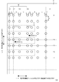
- FIG. 1 is a layout diagram of conductive particles in the anisotropic conductive film 1A of the example.
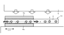
- FIG. 2 is a cross-sectional view at the time of anisotropic conductive connection using the anisotropic conductive film 1A of the example.
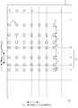
- FIG. 3 is an arrangement view of conductive particles in the anisotropic conductive film 1B of the example.
- FIG. 4 is an arrangement view of conductive particles in the anisotropic conductive film 1C of the example.
- FIG. 1 is an arrangement view of conductive particles 2 in an anisotropic conductive film 1A according to an embodiment of the present invention.
- the conductive particles 2 are arranged in a lattice pattern in the insulating adhesive layer 3 by arranging them in the first direction and the second direction. More specifically, the conductive particles 2 are arranged in a first direction parallel to the longitudinal direction L1 of the anisotropic conductive film 1A (S1, S2, S3, S4,...) And the anisotropic conductive film 1A. It arrange
- the array S in the first direction has a wide and narrow interval between adjacent arrays, and the wide and narrow are repeated. That is, when the distance between three adjacent arrays is a, b, c, a ⁇ b ⁇ c The unit U between the arrays is repeated.
- a ⁇ 0 and a 0, adjacent conductive particles are in contact with each other.
- the arrays T in the second direction are formed at equal intervals.
- the anisotropic conductive film 1A has a region where the arrangement density of the conductive particles 2 is sparse and a dense region due to the arrangement in the first direction and the arrangement in the second direction.
- the direction array T is preferably parallel, and the first direction array S is preferably crossed with the longitudinal direction of the terminal 4.
- the terminals are arranged so that the dense region of the conductive particles 2 of the anisotropic conductive film 1A is sandwiched between the terminal 4a of the first electronic component and the terminal 4b of the second electronic component.
- the conductive particles 2 on the terminals 4a and 4b are also horizontal.
- the conductive particles 2 located between terminals adjacent to each other also move in the direction of arrow A.
- the terminals 4a and 4b are generated even when the conductive particles 2 are removed from the terminals 4a and 4b due to the flow of the resin. Can capture enough conductive particles 2 to ensure electrical continuity. Therefore, the terminals 4a and 4b are connected by the conductive particles 2 as indicated by broken lines. Further, since there is a sparse region of the conductive particles 2 in the direction of the arrow A in the direction of the arrow A outside the region where the terminals are formed in parallel between the adjacent terminals, it is formed only in the dense region of the conductive particles 2.
- the conductive particles 2 can be prevented from being connected to each other, and in particular, the connection of three or more can be prevented. Therefore, it is possible to prevent a short circuit between the terminals adjacent in the horizontal direction by the connected conductive particles 2.
- the sum of the distances a, b, and c between the three adjacent arrays is larger than the length of the terminal 4 in the longitudinal direction so that the conductive particles 2 are reliably captured at each terminal 4 during anisotropic conductive connection. It is preferable to shorten it. This is because the presence of three or more conductive particles on the terminal is preferable in terms of stability of anisotropic connection.
- the distance b is preferably 0.5 times or more, more preferably 0.5 to 150 times the particle diameter of the conductive particles 2. It is even more preferable to set the ratio to 75 to 100 times.
- the distance c is preferably 0.5 ⁇ integer times the distance b. This is because the comparison with the distance b is easy.
- the distances a, b, and c have an isometric relationship.
- the particle diameter is set to an integral multiple of 1/2 of the particle diameter, the particles can be used as one reference (scale). Thereby, even after anisotropic conductive connection, it becomes easy to grasp the indentation uniformity, so that it is easy to determine a connection failure in the connection structure.
- the distance between the arrays T1, T2, T3, T4,... In the second direction parallel to the short direction of the anisotropic conductive film 1A is 0 in terms of the average diameter of the conductive particles from the viewpoint of suppressing short circuit and improving conduction reliability. It is preferable to make it 5 times or more. This distance is appropriately designed according to the bump layout of anisotropic connection. This is because the direction in which the molten resin flows at the time of anisotropic conductive connection cannot be predicted completely, and the resin flow may be random on or near the terminals.
- the particle diameter D of the conductive particles 2 is preferably 1 to 10 ⁇ m from the viewpoint of prevention of short circuit and the stability of bonding of opposing terminals.
- the density of the conductive particles 2 is preferably 2000 to 250,000 pieces / mm 2 . This particle density is appropriately adjusted according to the particle diameter and arrangement direction of the conductive particles 2.
- the constituent material of the conductive particles 2 itself, the layer configuration of the insulating adhesive layer 3, or the constituent resin can take various forms.
- the conductive particles 2 can be appropriately selected from those used in known anisotropic conductive films.
- examples thereof include metal particles such as nickel, cobalt, silver, copper, gold, and palladium, and metal-coated resin particles. Two or more kinds can be used in combination.
- an insulating resin layer used in a known anisotropic conductive film can be appropriately adopted.
- a photo radical polymerization type resin layer containing an acrylate compound and a photo radical polymerization initiator a heat radical polymerization type resin layer containing an acrylate compound and a heat radical polymerization initiator, a heat containing an epoxy compound and a heat cationic polymerization initiator
- a cationic polymerization type resin layer, a thermal anion polymerization type resin layer containing an epoxy compound and a thermal anion polymerization initiator, or the like can be used.
- these resin layers can be polymerized as necessary.
- the insulating adhesive layer 3 may be formed from a plurality of resin layers.
- the anisotropic conductive film of the present invention can take various forms.
- the arrangement S in the first direction parallel to the longitudinal direction L1 of the anisotropic conductive film is equally spaced, You may give wide and narrow the space
- the distance b between the arrays T is 0.5 times or more the particle diameter of the conductive particles 2 as with the distances a, b, and c between the arrays S in the anisotropic conductive film 1A described above. 0.5 to 150 times is more preferable, and 0.75 to 100 times is even more preferable. Moreover, it is preferable that the sum of the distances a, b, and c is less than 0.4 mm.
- the spacing between the arrays S in the first direction is preferably 0.5 times or more the particle diameter of the conductive particles 2, and more preferably an integer multiple of 1/2 of the particle diameter. preferable. This is because the arrangement of the conductive particles can be used as one standard (scale) for determining the state after anisotropic conductive connection.
- the length of the bump may exceed the short direction (width) of the film, there is no need to set an upper limit on the number of conductive particles existing in the length direction of the bump. It is preferable that there are 3 or more conductive particles, and more preferably 4 or more in the short direction (width).
- the terminal 4 When the resin melted at the time of anisotropic conductive connection flows in the short direction of the terminal 4 by making the interval of the array T in the second direction wide and narrow like this anisotropic conductive film 1B, the terminal 4 The trapping property of the conductive particles 2 can be ensured, and the occurrence of short circuit can be suppressed.
- the spacing between the arrays S in the first direction parallel to the longitudinal direction L1 of the anisotropic conductive film is wide.
- the interval of the array T in the second direction parallel to the short direction of the anisotropic conductive film 1A may be widened.
- the resin melted on or in the vicinity of the terminal 4 at the time of anisotropic conductive connection is randomized by providing a wide and narrow space between the array S in the first direction and the space between the arrays T in the second direction. Even if it flows in the direction, it is possible to secure the trapping property of the conductive particles 2 at the terminals 4 and suppress the occurrence of short circuit.
- the unit to be repeated is 2 You may comprise only the distance a and b between two arrangement
- the distance between the arrangements a ⁇ b ⁇ c Is preferably included. This is because, when there are three or more distance settings between the arrays, it becomes easier to distinguish between long and short than in the case of two. This is particularly effective when the difference between the distances a and b is relatively small.
- the distance c between the arrays may be a distance between two arrays when the distance between the arrays is not wide, and one array may be repeatedly lost in the arrangement of the grid-like conductive particles. Good.
- the array S in the first direction and the array T in the second direction do not have to be orthogonal.
- One or both of the arrays may be inclined with respect to the longitudinal direction of the anisotropic conductive film.
- the same rectangular terminals 4 are generally arranged at a predetermined interval in one direction, and therefore the first direction array S or the second direction array T.
- a mold having a dent corresponding to the arrangement of the conductive particles 2 is produced by a known method such as machining, laser processing, or photolithography. Conductive particles are put into a mold, and an insulating adhesive layer forming composition is filled thereon, cured, and taken out of the mold. From such a mold, the mold may be made of a material having lower rigidity.
- a member in which through holes are formed in a predetermined arrangement is provided on the insulating adhesive layer forming composition layer.
- the conductive particles 2 may be supplied from the through holes and passed through the through holes.
- the terminal of the first electronic component such as an IC chip, IC module, or liquid crystal panel and the terminal of the second electronic component such as a flexible substrate are anisotropically conductively connected, or the IC
- anisotropic conductive connection between the terminals of the first electronic component such as a chip and an IC module and the terminals of the second electronic component such as a glass substrate, as shown in FIG.
- a dense region is disposed between the opposing terminals 4.
- the present invention also includes a connection structure thus connected.
- an array having a wide and narrow interval between the conductive particles so as to cross the longitudinal direction of the terminals in terms of preventing a short circuit between the terminals in the connection structure.
- Examples 1 to 10, Comparative Examples 1 and 2 In order to investigate the relationship between the arrangement of the conductive particles and the conduction characteristics in the anisotropic conductive film, an anisotropic conductive film having the arrangement shown in Table 1 was produced.
- AUL704 manufactured by Sekisui Chemical Co., Ltd. and a particle size of 4 ⁇ m are used as the conductive particles
- the insulating adhesive layer is composed of 60 parts by mass of TP-50 (thermoplastic resin) manufactured by Nippon Steel & Sumikin Chemical Co., Ltd. and Mitsubishi Chemical. It was formed as follows from a mixed solution containing 60 parts by mass of jER828 (thermosetting resin) manufactured by Co., Ltd.
- SI-60L selective curing agent manufactured by Sanshin Chemical Industry Co., Ltd. That is, this mixed solution was applied onto a PET film having a film thickness of 50 ⁇ m and dried in an oven at 80 ° C. for 5 minutes to form an adhesive layer having a thickness of 20 ⁇ m on the PET film.
- a mold having an arrangement pattern of convex portions is prepared in the arrangement shown in Table 1, and a well-known transparent resin pellet is poured into a molten state in a melted state, cooled and solidified, whereby the concave portions are formed in Table 1.
- a resin mold having the arrangement pattern shown in FIG. The resin-type recess was filled with conductive particles, and the adhesive layer of the above-mentioned insulating adhesive layer was covered thereon, and the curable resin contained in the insulating adhesive layer was cured by ultraviolet curing. And the insulation adhesive layer was peeled from the type
- Comparative Example 1 the conductive particles were dispersed and sprayed in a low boiling point solvent and randomly arranged on the same plane.
- the terminal patterns of the FPC and the glass substrate correspond to each other, and the sizes are as follows. Further, the longitudinal direction of the anisotropic conductive film and the short direction of the bumps were bonded together.
- connection object for evaluation produced in (a) using the anisotropic conductive film of each Example and Comparative Example was placed in a thermostatic bath having a temperature of 85 ° C. and a humidity of 85% RH for 500 hours.
- the conduction resistance was measured in the same manner as (a). In addition, it is not preferable that this conduction resistance exceeds 5 ⁇ from the viewpoint of practical conduction stability of the connected electronic component.
- the anisotropic conductive films of Examples 2, 3, 5, 6, 8, 9, and 10 have a smaller number density of conductive particles than the anisotropic conductive films of Comparative Examples 1 and 2,
- it has the same initial conductivity and conduction reliability as the connected objects for evaluation in Comparative Examples 1 and 2, and can reduce the number of conductive particles necessary to ensure conductivity, and is anisotropic. It can be seen that the manufacturing cost of the conductive film can be reduced.
Landscapes
- Chemical & Material Sciences (AREA)
- Organic Chemistry (AREA)
- Chemical Kinetics & Catalysis (AREA)
- Health & Medical Sciences (AREA)
- Medicinal Chemistry (AREA)
- Polymers & Plastics (AREA)
- Physics & Mathematics (AREA)
- Dispersion Chemistry (AREA)
- Spectroscopy & Molecular Physics (AREA)
- Inorganic Chemistry (AREA)
- Engineering & Computer Science (AREA)
- Microelectronics & Electronic Packaging (AREA)
- Manufacturing & Machinery (AREA)
- Non-Insulated Conductors (AREA)
- Wire Bonding (AREA)
Abstract
Description
a<b<c
となる配列間のユニットUが繰り返されている。ここで、a≧0であり、a=0の場合、隣り合う導電粒子が接触していることになる。
異方性導電フィルムにおける導電粒子の配置と導通特性の関係を調べるために、表1に示す配置の異方性導電フィルムを製造した。この場合、導電粒子として積水化学工業(株)製AUL704、粒径4μmを使用し、絶縁接着剤層を、新日鉄住金化学(株)製TP-50(熱可塑性樹脂)60質量部と、三菱化学(株)製jER828(熱硬化性樹脂)60質量部と、三新化学工業(株)製SI-60L(潜在性硬化剤)2質量を含む混合溶液から次のように形成した。即ち、この混合液をフィルム厚50μmのPETフィルム上に塗布し、80℃のオーブンにて5分間乾燥させ、PETフィルム上に厚み20μmの粘着層を形成した。
各実施例及び比較例の異方性導電フィルムの(a)初期導通抵抗、(b)導通信頼性、(c)連結粒子塊数を、それぞれ次のように評価した。結果を表1に示す。
(a)初期導通抵抗
各実施例及び比較例の異方性導電フィルムを、フレキシブル基板(FPC)とガラス基板の間に挟み、加熱加圧(180℃、80MPa、5秒)して各評価用接続物を得、この評価用接続物の導通抵抗を測定した。
また、異方性導電フィルムの長手方向とバンプの短手方向を合わせて貼り合わせた。
バンプピッチ:32μm
バンプ幅:16μm、バンプ間スペース:16μm
バンプ長さ:1mm
ITOベタガラス
各実施例及び比較例の異方性導電フィルムを用いて(a)で作製した評価用接続物を温度85℃、湿度85%RHの恒温槽に500時間おいた後の導通抵抗を、(a)と同様に測定した。なお、この導通抵抗が5Ωを超えると、接続した電子部品の実用的な導通安定性の点から好ましくない。
各実施例及び比較例の異方性導電フィルムを用いて(a)で作製した評価用接続物を顕微鏡観察し、導電粒子が2個以上連結している連結粒子塊の個数を数え、導電粒子100個あたりの連結粒子塊の個数を求めた。

2 導電粒子
3 絶縁接着剤層
4、4a、4b 端子
5 ヒーター
a、b、c 配列間の距離
L1 異方性導電フィルムの長手方向
L2 異方性導電フィルムの短手方向(接続端子の長手方向)
S、S1、S2、S2、S4 第1方向の配列
T、T1、T2、T3、T4 第2方向の配列
U 配列間のユニット
D 導電粒子の粒子径
Claims (9)
- 絶縁接着剤層と、該絶縁接着剤層に配置された導電粒子を含む異方性導電フィルムであって、導電粒子が第1方向と第2方向に配列することにより格子状に配置されており、少なくとも一方向の配列において、隣接する配列の間隔に広狭を有する異方性導電フィルム。
- 隣接する3つの配列間の距離をa、b、cとした場合に、少なくとも一方向の配列に
a<b<c
となる配列間ユニットを有する請求項1記載の異方性導電フィルム。 - 配列の間隔に広狭を繰り返し有する請求項1又は2記載の異方性導電フィルム。
- 配列の間隔に広狭を有する配列が、異方性導電フィルムの長手方向と平行である請求項1~3のいずれかに記載の異方性導電フィルム。
- 配列間ユニットにおいて配列間の距離が等比的に変化している請求項2~4のいずれかに記載の異方性導電フィルム。
- 距離bが、導電粒子の粒子径の0.5倍以上である請求項2~5のいずれかに記載の異方性導電フィルム。
- 請求項1~6のいずれかに記載の異方性導電フィルムを用いて第1電子部品の端子と第2電子部品の端子を異方性導電接続する接続方法であって、異方性導電フィルムにおける導電粒子の配列の間隔に広狭があることにより形成される導電粒子の疎な領域と密な領域のうち密な領域を対向する端子間に配置する接続方法。
- 配列の間隔に広狭を有する配列を、端子の長手方向と交叉するように配置する請求項7記載の接続方法。
- 請求項7又は8に記載の接続方法により第1の電子部品と第2の電子部品が異方性導電接続されている接続構造体。
Priority Applications (3)
| Application Number | Priority Date | Filing Date | Title |
|---|---|---|---|
| CN201580055622.7A CN106797081B (zh) | 2014-10-28 | 2015-10-02 | 各向异性导电膜及连接结构体 |
| KR1020177000103A KR102519777B1 (ko) | 2014-10-28 | 2015-10-02 | 이방성 도전 필름 및 접속 구조체 |
| US15/509,359 US10975267B2 (en) | 2014-10-28 | 2015-10-02 | Anisotropic conductive film and connection structure |
Applications Claiming Priority (2)
| Application Number | Priority Date | Filing Date | Title |
|---|---|---|---|
| JP2014219785A JP6476747B2 (ja) | 2014-10-28 | 2014-10-28 | 異方性導電フィルム及び接続構造体 |
| JP2014-219785 | 2014-10-28 |
Publications (1)
| Publication Number | Publication Date |
|---|---|
| WO2016067828A1 true WO2016067828A1 (ja) | 2016-05-06 |
Family
ID=55857172
Family Applications (1)
| Application Number | Title | Priority Date | Filing Date |
|---|---|---|---|
| PCT/JP2015/078012 Ceased WO2016067828A1 (ja) | 2014-10-28 | 2015-10-02 | 異方性導電フィルム及び接続構造体 |
Country Status (6)
| Country | Link |
|---|---|
| US (1) | US10975267B2 (ja) |
| JP (1) | JP6476747B2 (ja) |
| KR (1) | KR102519777B1 (ja) |
| CN (1) | CN106797081B (ja) |
| TW (1) | TWI675088B (ja) |
| WO (1) | WO2016067828A1 (ja) |
Cited By (1)
| Publication number | Priority date | Publication date | Assignee | Title |
|---|---|---|---|---|
| US20230118485A1 (en) * | 2020-02-12 | 2023-04-20 | Dexerials Corporation | Anisotropic conductive film |
Families Citing this family (10)
| Publication number | Priority date | Publication date | Assignee | Title |
|---|---|---|---|---|
| TWI785642B (zh) | 2014-11-17 | 2022-12-01 | 日商迪睿合股份有限公司 | 異向性導電膜及連接構造體 |
| JP6759578B2 (ja) * | 2014-12-22 | 2020-09-23 | デクセリアルズ株式会社 | 異方導電性フィルム及び接続構造体 |
| KR102535557B1 (ko) * | 2016-03-07 | 2023-05-24 | 삼성디스플레이 주식회사 | 표시 장치 및 전자 디바이스 |
| CN114907594B (zh) * | 2016-10-31 | 2025-07-22 | 迪睿合株式会社 | 含填料膜 |
| WO2018101108A1 (ja) * | 2016-12-01 | 2018-06-07 | デクセリアルズ株式会社 | 異方性導電フィルム |
| TWI763750B (zh) * | 2016-12-01 | 2022-05-11 | 日商迪睿合股份有限公司 | 異向性導電膜 |
| CN107452438B (zh) | 2017-07-27 | 2019-10-11 | 京东方科技集团股份有限公司 | 一种各向异性导电胶带及胶带卷、绑定结构及显示装置 |
| US20190100663A1 (en) * | 2017-10-03 | 2019-04-04 | Shin-Etsu Chemical Co., Ltd. | Anisotropic conductive film and method for manufacturing anisotropic conductive film |
| IL292146A (en) * | 2019-10-15 | 2022-06-01 | Univ Kyoto | Conductive layer, dispersion, manufacturing methods therefor and a device comprising a conductive layer |
| JP6824372B1 (ja) * | 2019-12-17 | 2021-02-03 | 三菱電機株式会社 | 絶縁シート及びその製造方法、並びに回転電機 |
Citations (3)
| Publication number | Priority date | Publication date | Assignee | Title |
|---|---|---|---|---|
| JP2003286457A (ja) * | 2002-03-28 | 2003-10-10 | Asahi Kasei Corp | 異方導電性接着シートおよびその製造方法 |
| JP2007080522A (ja) * | 2005-09-09 | 2007-03-29 | Sumitomo Bakelite Co Ltd | 異方導電性フィルムおよび電子・電機機器 |
| JP2014063729A (ja) * | 2012-08-29 | 2014-04-10 | Dexerials Corp | 異方性導電フィルム及びその製造方法 |
Family Cites Families (10)
| Publication number | Priority date | Publication date | Assignee | Title |
|---|---|---|---|---|
| US5672400A (en) * | 1995-12-21 | 1997-09-30 | Minnesota Mining And Manufacturing Company | Electronic assembly with semi-crystalline copolymer adhesive |
| JPH09320345A (ja) * | 1996-05-31 | 1997-12-12 | Whitaker Corp:The | 異方導電性フィルム |
| US20010008169A1 (en) * | 1998-06-30 | 2001-07-19 | 3M Innovative Properties Company | Fine pitch anisotropic conductive adhesive |
| JP3826605B2 (ja) * | 1999-03-08 | 2006-09-27 | セイコーエプソン株式会社 | 半導体装置の実装構造の製造方法、液晶装置、および電子機器 |
| DE60314164T2 (de) * | 2002-08-09 | 2008-02-07 | Jsr Corp. | Prüfverbinder mit anisotroper leitfähigkeit |
| KR20110036733A (ko) * | 2008-07-11 | 2011-04-08 | 소니 케미카루 앤드 인포메이션 디바이스 가부시키가이샤 | 이방성 도전 필름 |
| KR20170044766A (ko) * | 2012-08-01 | 2017-04-25 | 데쿠세리아루즈 가부시키가이샤 | 이방성 도전 필름의 제조 방법, 이방성 도전 필름, 및 접속 구조체 |
| JP2015149451A (ja) * | 2014-02-07 | 2015-08-20 | デクセリアルズ株式会社 | アライメント方法、電子部品の接続方法、接続体の製造方法、接続体、異方性導電フィルム |
| JP6661888B2 (ja) * | 2014-03-31 | 2020-03-11 | デクセリアルズ株式会社 | 異方性導電フィルムの製造方法 |
| JP2016029698A (ja) * | 2014-07-22 | 2016-03-03 | デクセリアルズ株式会社 | 接続体、及び接続体の製造方法 |
-
2014
- 2014-10-28 JP JP2014219785A patent/JP6476747B2/ja active Active
-
2015
- 2015-10-02 US US15/509,359 patent/US10975267B2/en active Active
- 2015-10-02 KR KR1020177000103A patent/KR102519777B1/ko active Active
- 2015-10-02 CN CN201580055622.7A patent/CN106797081B/zh active Active
- 2015-10-02 WO PCT/JP2015/078012 patent/WO2016067828A1/ja not_active Ceased
- 2015-10-08 TW TW104133174A patent/TWI675088B/zh active
Patent Citations (3)
| Publication number | Priority date | Publication date | Assignee | Title |
|---|---|---|---|---|
| JP2003286457A (ja) * | 2002-03-28 | 2003-10-10 | Asahi Kasei Corp | 異方導電性接着シートおよびその製造方法 |
| JP2007080522A (ja) * | 2005-09-09 | 2007-03-29 | Sumitomo Bakelite Co Ltd | 異方導電性フィルムおよび電子・電機機器 |
| JP2014063729A (ja) * | 2012-08-29 | 2014-04-10 | Dexerials Corp | 異方性導電フィルム及びその製造方法 |
Cited By (2)
| Publication number | Priority date | Publication date | Assignee | Title |
|---|---|---|---|---|
| US20230118485A1 (en) * | 2020-02-12 | 2023-04-20 | Dexerials Corporation | Anisotropic conductive film |
| US12590194B2 (en) * | 2020-02-12 | 2026-03-31 | Dexerials Corporation | Anisotropic conductive film |
Also Published As
| Publication number | Publication date |
|---|---|
| CN106797081A (zh) | 2017-05-31 |
| KR102519777B1 (ko) | 2023-04-07 |
| US20170278820A1 (en) | 2017-09-28 |
| TWI675088B (zh) | 2019-10-21 |
| KR20170072182A (ko) | 2017-06-26 |
| JP6476747B2 (ja) | 2019-03-06 |
| JP2016085931A (ja) | 2016-05-19 |
| CN106797081B (zh) | 2019-04-16 |
| US10975267B2 (en) | 2021-04-13 |
| TW201627438A (zh) | 2016-08-01 |
Similar Documents
| Publication | Publication Date | Title |
|---|---|---|
| JP6476747B2 (ja) | 異方性導電フィルム及び接続構造体 | |
| JP6932110B2 (ja) | 異方導電性フィルム及び接続構造体 | |
| US11923335B2 (en) | Anisotropic conductive film and connected structure | |
| US20170352636A1 (en) | Anisotropic conductive film and connection structure | |
| WO2016002336A1 (ja) | 異方導電性フィルム及び接続構造体 | |
| HK40073081A (en) | Anisotropic conductive film and connected structure | |
| HK1234207A1 (en) | Anisotropic conductive film and connection structure | |
| HK1234207B (zh) | 各向异性导电膜及连接结构体 | |
| HK1257883B (en) | Anisotropic electroconductive film and connection structure | |
| HK1241136A1 (en) | Anisotropic electroconductive film and connection structure | |
| HK1225169A1 (en) | Anisotropic electroconductive film and connection structure | |
| HK1233386A1 (en) | Anisotropically-conductive film and connection structure |
Legal Events
| Date | Code | Title | Description |
|---|---|---|---|
| 121 | Ep: the epo has been informed by wipo that ep was designated in this application |
Ref document number: 15855009 Country of ref document: EP Kind code of ref document: A1 |
|
| DPE1 | Request for preliminary examination filed after expiration of 19th month from priority date (pct application filed from 20040101) | ||
| ENP | Entry into the national phase |
Ref document number: 20177000103 Country of ref document: KR Kind code of ref document: A |
|
| WWE | Wipo information: entry into national phase |
Ref document number: 15509359 Country of ref document: US |
|
| NENP | Non-entry into the national phase |
Ref country code: DE |
|
| 122 | Ep: pct application non-entry in european phase |
Ref document number: 15855009 Country of ref document: EP Kind code of ref document: A1 |