WO2016059871A1 - 炭化珪素半導体装置およびその製造方法 - Google Patents
炭化珪素半導体装置およびその製造方法 Download PDFInfo
- Publication number
- WO2016059871A1 WO2016059871A1 PCT/JP2015/073388 JP2015073388W WO2016059871A1 WO 2016059871 A1 WO2016059871 A1 WO 2016059871A1 JP 2015073388 W JP2015073388 W JP 2015073388W WO 2016059871 A1 WO2016059871 A1 WO 2016059871A1
- Authority
- WO
- WIPO (PCT)
- Prior art keywords
- region
- silicon carbide
- semiconductor region
- base
- epitaxial layer
- Prior art date
- Legal status (The legal status is an assumption and is not a legal conclusion. Google has not performed a legal analysis and makes no representation as to the accuracy of the status listed.)
- Ceased
Links
Images








Classifications
-
- H—ELECTRICITY
- H10—SEMICONDUCTOR DEVICES; ELECTRIC SOLID-STATE DEVICES NOT OTHERWISE PROVIDED FOR
- H10D—INORGANIC ELECTRIC SEMICONDUCTOR DEVICES
- H10D84/00—Integrated devices formed in or on semiconductor substrates that comprise only semiconducting layers, e.g. on Si wafers or on GaAs-on-Si wafers
- H10D84/40—Integrated devices formed in or on semiconductor substrates that comprise only semiconducting layers, e.g. on Si wafers or on GaAs-on-Si wafers characterised by the integration of at least one component covered by groups H10D12/00 or H10D30/00 with at least one component covered by groups H10D10/00 or H10D18/00, e.g. integration of IGFETs with BJTs
-
- H—ELECTRICITY
- H10—SEMICONDUCTOR DEVICES; ELECTRIC SOLID-STATE DEVICES NOT OTHERWISE PROVIDED FOR
- H10D—INORGANIC ELECTRIC SEMICONDUCTOR DEVICES
- H10D12/00—Bipolar devices controlled by the field effect, e.g. insulated-gate bipolar transistors [IGBT]
- H10D12/01—Manufacture or treatment
- H10D12/031—Manufacture or treatment of IGBTs
-
- H—ELECTRICITY
- H10—SEMICONDUCTOR DEVICES; ELECTRIC SOLID-STATE DEVICES NOT OTHERWISE PROVIDED FOR
- H10D—INORGANIC ELECTRIC SEMICONDUCTOR DEVICES
- H10D30/00—Field-effect transistors [FET]
- H10D30/60—Insulated-gate field-effect transistors [IGFET]
-
- H—ELECTRICITY
- H10—SEMICONDUCTOR DEVICES; ELECTRIC SOLID-STATE DEVICES NOT OTHERWISE PROVIDED FOR
- H10D—INORGANIC ELECTRIC SEMICONDUCTOR DEVICES
- H10D30/00—Field-effect transistors [FET]
- H10D30/60—Insulated-gate field-effect transistors [IGFET]
- H10D30/64—Double-diffused metal-oxide semiconductor [DMOS] FETs
- H10D30/66—Vertical DMOS [VDMOS] FETs
- H10D30/662—Vertical DMOS [VDMOS] FETs having a drift region having a doping concentration that is higher between adjacent body regions relative to other parts of the drift region
-
- H—ELECTRICITY
- H10—SEMICONDUCTOR DEVICES; ELECTRIC SOLID-STATE DEVICES NOT OTHERWISE PROVIDED FOR
- H10D—INORGANIC ELECTRIC SEMICONDUCTOR DEVICES
- H10D30/00—Field-effect transistors [FET]
- H10D30/60—Insulated-gate field-effect transistors [IGFET]
- H10D30/64—Double-diffused metal-oxide semiconductor [DMOS] FETs
- H10D30/66—Vertical DMOS [VDMOS] FETs
- H10D30/665—Vertical DMOS [VDMOS] FETs having edge termination structures
-
- H—ELECTRICITY
- H10—SEMICONDUCTOR DEVICES; ELECTRIC SOLID-STATE DEVICES NOT OTHERWISE PROVIDED FOR
- H10D—INORGANIC ELECTRIC SEMICONDUCTOR DEVICES
- H10D62/00—Semiconductor bodies, or regions thereof, of devices having potential barriers
- H10D62/10—Shapes, relative sizes or dispositions of the regions of the semiconductor bodies; Shapes of the semiconductor bodies
-
- H—ELECTRICITY
- H10—SEMICONDUCTOR DEVICES; ELECTRIC SOLID-STATE DEVICES NOT OTHERWISE PROVIDED FOR
- H10D—INORGANIC ELECTRIC SEMICONDUCTOR DEVICES
- H10D62/00—Semiconductor bodies, or regions thereof, of devices having potential barriers
- H10D62/10—Shapes, relative sizes or dispositions of the regions of the semiconductor bodies; Shapes of the semiconductor bodies
- H10D62/102—Constructional design considerations for preventing surface leakage or controlling electric field concentration
- H10D62/103—Constructional design considerations for preventing surface leakage or controlling electric field concentration for increasing or controlling the breakdown voltage of reverse-biased devices
- H10D62/104—Constructional design considerations for preventing surface leakage or controlling electric field concentration for increasing or controlling the breakdown voltage of reverse-biased devices having particular shapes of the bodies at or near reverse-biased junctions, e.g. having bevels or moats
-
- H—ELECTRICITY
- H10—SEMICONDUCTOR DEVICES; ELECTRIC SOLID-STATE DEVICES NOT OTHERWISE PROVIDED FOR
- H10D—INORGANIC ELECTRIC SEMICONDUCTOR DEVICES
- H10D62/00—Semiconductor bodies, or regions thereof, of devices having potential barriers
- H10D62/10—Shapes, relative sizes or dispositions of the regions of the semiconductor bodies; Shapes of the semiconductor bodies
- H10D62/102—Constructional design considerations for preventing surface leakage or controlling electric field concentration
- H10D62/103—Constructional design considerations for preventing surface leakage or controlling electric field concentration for increasing or controlling the breakdown voltage of reverse-biased devices
- H10D62/105—Constructional design considerations for preventing surface leakage or controlling electric field concentration for increasing or controlling the breakdown voltage of reverse-biased devices by having particular doping profiles, shapes or arrangements of PN junctions; by having supplementary regions, e.g. junction termination extension [JTE]
-
- H—ELECTRICITY
- H10—SEMICONDUCTOR DEVICES; ELECTRIC SOLID-STATE DEVICES NOT OTHERWISE PROVIDED FOR
- H10D—INORGANIC ELECTRIC SEMICONDUCTOR DEVICES
- H10D62/00—Semiconductor bodies, or regions thereof, of devices having potential barriers
- H10D62/10—Shapes, relative sizes or dispositions of the regions of the semiconductor bodies; Shapes of the semiconductor bodies
- H10D62/17—Semiconductor regions connected to electrodes not carrying current to be rectified, amplified or switched, e.g. channel regions
- H10D62/393—Body regions of DMOS transistors or IGBTs
-
- H—ELECTRICITY
- H10—SEMICONDUCTOR DEVICES; ELECTRIC SOLID-STATE DEVICES NOT OTHERWISE PROVIDED FOR
- H10D—INORGANIC ELECTRIC SEMICONDUCTOR DEVICES
- H10D62/00—Semiconductor bodies, or regions thereof, of devices having potential barriers
- H10D62/80—Semiconductor bodies, or regions thereof, of devices having potential barriers characterised by the materials
- H10D62/81—Semiconductor bodies, or regions thereof, of devices having potential barriers characterised by the materials of structures exhibiting quantum-confinement effects, e.g. single quantum wells; of structures having periodic or quasi-periodic potential variation
-
- H—ELECTRICITY
- H10—SEMICONDUCTOR DEVICES; ELECTRIC SOLID-STATE DEVICES NOT OTHERWISE PROVIDED FOR
- H10D—INORGANIC ELECTRIC SEMICONDUCTOR DEVICES
- H10D62/00—Semiconductor bodies, or regions thereof, of devices having potential barriers
- H10D62/80—Semiconductor bodies, or regions thereof, of devices having potential barriers characterised by the materials
- H10D62/83—Semiconductor bodies, or regions thereof, of devices having potential barriers characterised by the materials being Group IV materials, e.g. B-doped Si or undoped Ge
- H10D62/832—Semiconductor bodies, or regions thereof, of devices having potential barriers characterised by the materials being Group IV materials, e.g. B-doped Si or undoped Ge being Group IV materials comprising two or more elements, e.g. SiGe
- H10D62/8325—Silicon carbide
-
- H—ELECTRICITY
- H10—SEMICONDUCTOR DEVICES; ELECTRIC SOLID-STATE DEVICES NOT OTHERWISE PROVIDED FOR
- H10D—INORGANIC ELECTRIC SEMICONDUCTOR DEVICES
- H10D84/00—Integrated devices formed in or on semiconductor substrates that comprise only semiconducting layers, e.g. on Si wafers or on GaAs-on-Si wafers
- H10D84/01—Manufacture or treatment
- H10D84/02—Manufacture or treatment characterised by using material-based technologies
- H10D84/03—Manufacture or treatment characterised by using material-based technologies using Group IV technology, e.g. silicon technology or silicon-carbide [SiC] technology
- H10D84/035—Manufacture or treatment characterised by using material-based technologies using Group IV technology, e.g. silicon technology or silicon-carbide [SiC] technology using silicon carbide [SiC] technology
-
- H—ELECTRICITY
- H10—SEMICONDUCTOR DEVICES; ELECTRIC SOLID-STATE DEVICES NOT OTHERWISE PROVIDED FOR
- H10P—GENERIC PROCESSES OR APPARATUS FOR THE MANUFACTURE OR TREATMENT OF DEVICES COVERED BY CLASS H10
- H10P30/00—Ion implantation into wafers, substrates or parts of devices
- H10P30/20—Ion implantation into wafers, substrates or parts of devices into semiconductor materials, e.g. for doping
- H10P30/202—Ion implantation into wafers, substrates or parts of devices into semiconductor materials, e.g. for doping characterised by the semiconductor materials
- H10P30/204—Ion implantation into wafers, substrates or parts of devices into semiconductor materials, e.g. for doping characterised by the semiconductor materials into Group IV semiconductors
- H10P30/2042—Ion implantation into wafers, substrates or parts of devices into semiconductor materials, e.g. for doping characterised by the semiconductor materials into Group IV semiconductors into crystalline silicon carbide
-
- H—ELECTRICITY
- H10—SEMICONDUCTOR DEVICES; ELECTRIC SOLID-STATE DEVICES NOT OTHERWISE PROVIDED FOR
- H10P—GENERIC PROCESSES OR APPARATUS FOR THE MANUFACTURE OR TREATMENT OF DEVICES COVERED BY CLASS H10
- H10P30/00—Ion implantation into wafers, substrates or parts of devices
- H10P30/20—Ion implantation into wafers, substrates or parts of devices into semiconductor materials, e.g. for doping
- H10P30/21—Ion implantation into wafers, substrates or parts of devices into semiconductor materials, e.g. for doping of electrically active species
-
- H—ELECTRICITY
- H10—SEMICONDUCTOR DEVICES; ELECTRIC SOLID-STATE DEVICES NOT OTHERWISE PROVIDED FOR
- H10P—GENERIC PROCESSES OR APPARATUS FOR THE MANUFACTURE OR TREATMENT OF DEVICES COVERED BY CLASS H10
- H10P30/00—Ion implantation into wafers, substrates or parts of devices
- H10P30/20—Ion implantation into wafers, substrates or parts of devices into semiconductor materials, e.g. for doping
- H10P30/28—Ion implantation into wafers, substrates or parts of devices into semiconductor materials, e.g. for doping characterised by an annealing step, e.g. for activation of dopants
-
- H—ELECTRICITY
- H10—SEMICONDUCTOR DEVICES; ELECTRIC SOLID-STATE DEVICES NOT OTHERWISE PROVIDED FOR
- H10D—INORGANIC ELECTRIC SEMICONDUCTOR DEVICES
- H10D30/00—Field-effect transistors [FET]
- H10D30/80—FETs having rectifying junction gate electrodes
- H10D30/83—FETs having PN junction gate electrodes
-
- H—ELECTRICITY
- H10—SEMICONDUCTOR DEVICES; ELECTRIC SOLID-STATE DEVICES NOT OTHERWISE PROVIDED FOR
- H10D—INORGANIC ELECTRIC SEMICONDUCTOR DEVICES
- H10D62/00—Semiconductor bodies, or regions thereof, of devices having potential barriers
- H10D62/10—Shapes, relative sizes or dispositions of the regions of the semiconductor bodies; Shapes of the semiconductor bodies
- H10D62/13—Semiconductor regions connected to electrodes carrying current to be rectified, amplified or switched, e.g. source or drain regions
- H10D62/149—Source or drain regions of field-effect devices
- H10D62/151—Source or drain regions of field-effect devices of IGFETs
- H10D62/156—Drain regions of DMOS transistors
- H10D62/157—Impurity concentrations or distributions
Definitions
- the present invention relates to a silicon carbide semiconductor device formed using a wide band gap substrate and a method for manufacturing the same.
- silicon has been used as a constituent material of power semiconductor devices that control high voltage and large current.
- power semiconductor devices such as bipolar transistors, IGBTs (insulated gate bipolar transistors), MOSFETs (insulated gate field effect transistors), and these are properly used in accordance with applications.
- bipolar transistors and IGBTs have a higher current density than MOSFETs and can increase current, but they cannot perform high-speed switching operations.
- the bipolar transistor is limited in use at a switching frequency of about several kHz
- the IGBT is limited in use at a switching frequency of about several tens of kHz.
- a power MOSFET has a lower current density than a bipolar transistor or IGBT and is difficult to increase in current, but can perform a high-speed switching operation up to several MHz.
- SiC silicon carbide
- Silicon carbide is a chemically very stable semiconductor material, has a wide band gap of 3 eV, and can be used extremely stably as a semiconductor even at high temperatures. Silicon carbide is expected to be a semiconductor material that can achieve high breakdown voltage and low on-resistance because the maximum electric field strength is one digit or more larger than that of silicon. Such features of silicon carbide also apply to, for example, gallium nitride (GaN), which is a semiconductor having a wide band gap (hereinafter referred to as a wide band gap semiconductor). As described above, a semiconductor device having a high breakdown voltage by using a wide band gap semiconductor is disclosed (for example, Non-Patent Document 2).
- GaN gallium nitride
- a high voltage is applied not only to an active region where an element structure is formed, but also to a voltage structure part that is provided in the periphery of the active region and retains a withstand voltage, and an electric field concentrates on the voltage structure part.
- the breakdown voltage of the high breakdown voltage semiconductor device is determined by the impurity concentration, thickness, and electric field strength of the semiconductor.
- the breakdown tolerance determined by the characteristic features of the semiconductor is equal from the active region to the breakdown voltage structure. For this reason, when an electric field concentrates on a pressure
- FIG. 22 is a main part cross-sectional view of conventional silicon carbide semiconductor device 200.
- This silicon carbide semiconductor device 200 is exemplified by an N-channel MOSFET which is a switching device.
- silicon carbide may be referred to as SiC.
- Silicon carbide semiconductor device 200 includes an n-type SiC layer 52 disposed on the surface of n-type SiC substrate 51, a plurality of p-type regions 60 disposed on the surface of n-type SiC layer 52, and p-type region 60 A p-type SiC layer 61 is provided. Further, an n-type region 62 to be a JFET (junction field effect transistor) region disposed in the p-type SiC layer 61 on the n-type SiC layer 52 where the p-type region 60 is not formed, and the surface of the p-type SiC layer 61 Are provided with an n-type source region 54 and a p-type contact region 55. A source electrode 58 is provided on the surfaces of the n-type source region 54 and the p-type contact region 55.
- JFET junction field effect transistor
- a gate electrode 57 disposed on the surface of the p-type SiC layer 61 sandwiched between the n-type source region 54 and the n-type region 62 via the gate insulating film 56 and disposed on the back side of the n-type SiC substrate 51.
- a drain electrode 59 is provided.
- silicon carbide semiconductor device 200 when a voltage equal to or lower than the gate threshold is applied to gate electrode 57 with a positive voltage applied to drain electrode 59 with respect to source electrode 58, p-type region 60 and n-type are applied.
- the pn junction between the SiC layer 52 or the p-type SiC layer 61 and the n-type region 62 is reverse-biased, the breakdown voltage of the active region 201 is ensured, and no current flows.
- Silicon carbide semiconductor device 200 can perform a switching operation by a voltage applied to gate electrode 57.
- the p regions 81 and 82 and the p-type region sandwich the stepped portion.
- the electric field sharing of 60 is different, and the stepped portion 90 causes a decrease in breakdown voltage.
- the breakdown voltage is reduced due to the shape of the stepped portion 90 generated when the p-type SiC layer 61 is etched and the variation in impurity concentration on the surfaces of the p regions 81 and 82.
- the thickness of the n type SiC layer 52 under the p regions 81 and 82 is reduced.
- the avalanche is likely to occur at 81 and 82, and the breakdown voltage at the breakdown voltage structure 202 is lower than that of the active region 201.
- the area of the breakdown voltage structure 202 is smaller than that of the active region 201, the current density due to avalanche becomes excessive, and avalanche breakdown is likely to occur.
- An object of the present invention is to provide a silicon carbide semiconductor device that solves the above-described problems and prevents a decrease in breakdown voltage in a breakdown voltage structure and a method for manufacturing the same.
- the second conductivity type second base region, the first conductivity type source region, and the second conductivity type contact region may be disposed on the first base region.
- the contact region of the second conductivity type may be higher in concentration than the second base region.
- the silicon carbide semiconductor device may include a first conductivity type second drift region.
- the first conductivity type second drift region may be disposed between the second base region and the first silicon carbide epitaxial layer sandwiched between the first base regions.
- the silicon carbide semiconductor device may include a gate electrode.
- the gate electrode may be disposed on the second base region sandwiched between the source region and the second drift region via a gate insulating film.
- the silicon carbide semiconductor device may include a source electrode.
- the source electrode may be electrically connected to the source region and the contact region.
- the silicon carbide semiconductor device may include a drain electrode.
- the drain electrode may be electrically connected to the silicon carbide substrate.
- the silicon carbide semiconductor device may include a step portion. The step portion may be disposed on the outer periphery of the second base region and deeper than the bottom surface of the second base region and shallower than the bottom surface of the first base region.
- the silicon carbide semiconductor device may include a first semiconductor region (p region 33) of the second conductivity type.
- the second conductivity type first semiconductor region (p region 33) may be disposed on the surface layer of the first silicon carbide epitaxial layer, and may be in contact with the stepped portion, the second base region, and the first base region.
- the silicon carbide semiconductor device may include a second conductivity type second semiconductor region (p region 31).
- the second semiconductor region (p region 31) of the second conductivity type may be disposed on the surface layer of the first silicon carbide epitaxial layer below the bottom surface of the step portion and may be in contact with the first semiconductor region.
- the silicon carbide semiconductor device may include a second conductivity type third semiconductor region (p region 32).
- the third semiconductor region (p region 32) of the second conductivity type may be disposed on the surface layer of the first silicon carbide epitaxial layer below the bottom surface of the stepped portion and may be in contact with the second semiconductor region.
- the bottom surface of the first semiconductor region and the bottom surface of the first base region may be connected substantially flat.
- the impurity concentration of the first semiconductor region, the second semiconductor region, and the third semiconductor region may be lower than that of the first base region.
- the impurity concentration of the first semiconductor region may be higher than the impurity concentration of the second semiconductor region and the third semiconductor region.
- the impurity concentration of the first base region may be 4 ⁇ 10 17 cm ⁇ 3 or more and 1 ⁇ 10 18 cm ⁇ 3 or less.
- the difference between the bottom surfaces of the first base region, the first semiconductor region, the second semiconductor region, and the three semiconductor regions may be within ⁇ 0.1 ⁇ m.
- the impurity concentration of the first semiconductor region may be 2 ⁇ 10 16 cm ⁇ 3 or more and 1 ⁇ 10 17 cm ⁇ 3 or less.
- the impurity concentration of the second semiconductor region and the third semiconductor region may be 1 ⁇ 10 16 cm ⁇ 3 or more and 9 ⁇ 10 16 cm ⁇ 3 or less.
- a method for manufacturing a silicon carbide semiconductor device includes: a plurality of second conductivity type first base regions; a second conductivity type first semiconductor region; a second conductivity type second semiconductor region; and a second conductivity type third semiconductor region. May be formed so as to be in contact with each other. In this step, ions may be selectively implanted into the surface layer of the first conductivity type first silicon carbide epitaxial layer serving as the first drift region.
- the method for manufacturing the silicon carbide semiconductor device may include a step of forming the bottom surface of the first semiconductor region and the bottom surface of the first base region by connecting them substantially flat.
- the method for manufacturing the silicon carbide semiconductor device may include a step of forming a second conductivity type second silicon carbide epitaxial layer on the first silicon carbide epitaxial layer.
- the method for manufacturing a silicon carbide semiconductor device may include a step of forming a first conductivity type source region and a second conductivity type contact region. In this step, ions may be selectively implanted into the second silicon carbide epitaxial layer on the first base region.
- the method for manufacturing the silicon carbide semiconductor device may include a step of forming a first conductivity type second drift region. In this step, ions may be implanted into the second silicon carbide epitaxial layer on the first silicon carbide epitaxial layer sandwiched between the first base regions.
- the method for manufacturing a silicon carbide semiconductor device may include a step of setting a portion where ions are not implanted as a second base region.
- the method for manufacturing a silicon carbide semiconductor device includes: the second silicon carbide epitaxial layer formed on the first semiconductor region, the second semiconductor region, the third semiconductor region, and the first silicon carbide epitaxial layer in an outer peripheral portion; May be removed by etching.
- the method for manufacturing the silicon carbide semiconductor device may include a step of forming the step portion at the position of the first semiconductor region.
- the stepped portion may be deeper than the bottom surface of the second silicon carbide epitaxial layer and shallower than the bottom surface of the first base region.
- the impurity concentration of the first semiconductor region, the second semiconductor region, and the third semiconductor region may be lower than the impurity concentration of the first base region.
- the impurity concentration of the first semiconductor region may be higher than the impurity concentration of the second semiconductor region and the third semiconductor region.
- the impurity concentration of the first base region may be 4 ⁇ 10 17 cm ⁇ 3 or more and 1 ⁇ 10 18 cm ⁇ 3 or less.
- a method of manufacturing a silicon carbide semiconductor device includes: a plurality of second conductivity type first base regions; a second conductivity type second semiconductor region separated from the first base region; and a second conductivity type adjacent to the second semiconductor region. Forming a third semiconductor region. In this step, ions may be selectively implanted into the surface layer of the first conductivity type first silicon carbide epitaxial layer serving as the first drift region.
- the method for manufacturing the silicon carbide semiconductor device may include a step of forming a second conductivity type second silicon carbide epitaxial layer on the first silicon carbide epitaxial layer.
- the method for manufacturing a silicon carbide semiconductor device may include a step of forming a first conductivity type source region and a second conductivity type contact region.
- ions may be selectively implanted into the second silicon carbide epitaxial layer on the first base region.
- the method for manufacturing the silicon carbide semiconductor device may include a step of forming a first conductivity type second drift region. In this step, ions may be implanted into the second silicon carbide epitaxial layer on the first silicon carbide epitaxial layer sandwiched between the first base regions.
- the method for manufacturing a silicon carbide semiconductor device may include a step of setting a portion where ions are not implanted as a second base region.
- the method for manufacturing the silicon carbide semiconductor device may include a step of removing the second silicon carbide epitaxial layer on the outer peripheral side from the end portion of the first base region by etching.
- the method for manufacturing a silicon carbide semiconductor device may include a step of forming a stepped portion between the first base and the second semiconductor region.
- the stepped portion may be deeper than the bottom surface of the second silicon carbide epitaxial layer and shallower than the bottom surface of the first base region.
- the method for manufacturing the silicon carbide semiconductor device may include a step of forming the first semiconductor region.
- the first semiconductor region may be connected to the surface layer of the first silicon carbide epitaxial layer below the stepped portion, to the first base region, the second base region, and the second semiconductor region.
- the first semiconductor region may be connected substantially flat with the bottom of the first base region.
- the impurity concentration of the first semiconductor region, the second semiconductor region, and the third semiconductor region may be lower than the impurity concentration of the first base region.
- the impurity concentration of the first semiconductor region may be higher than the impurity concentration of the second semiconductor region and the third semiconductor region.
- the impurity concentration of the first base region may be 4 ⁇ 10 17 cm ⁇ 3 or more and 1 ⁇ 10 18 cm ⁇ 3 or less.
- the present invention it is possible to provide a silicon carbide semiconductor device and a method for manufacturing the same, in which a breakdown voltage drop in the breakdown voltage structure portion is prevented.
- FIG. 4 is a main-portion manufacturing process cross-sectional view of the silicon carbide semiconductor device 100 according to the second embodiment of the present invention continued from FIG. 3.
- FIG. 5 is a main-portion manufacturing process cross-sectional view of the silicon carbide semiconductor device 100 according to the second embodiment of the present invention continued from FIG. 4.
- FIG. 4 is a main-portion manufacturing process cross-sectional view of the silicon carbide semiconductor device 100 according to the second embodiment of the present invention continued from FIG. 4.
- FIG. 6 is a main-portion manufacturing process cross-sectional view of the silicon carbide semiconductor device 100 according to the second embodiment of the present invention continued from FIG. 5.
- FIG. 7 is a main-portion manufacturing process cross-sectional view of the silicon carbide semiconductor device 100 according to the second embodiment of the present invention continued from FIG. 6.
- FIG. 8 is a main-portion manufacturing process cross-sectional view of the silicon carbide semiconductor device 100 according to the second embodiment of the present invention continued from FIG. 7.
- FIG. 9 is a main-portion manufacturing process cross-sectional view of the silicon carbide semiconductor device 100 according to the second embodiment of the present invention continued from FIG. 8.
- FIG. 10 is a main-portion manufacturing process cross-sectional view of the silicon carbide semiconductor device 100 according to the second embodiment of the present invention continued from FIG. 9.
- FIG. 9 is a main-portion manufacturing process cross-sectional view of the silicon carbide semiconductor device 100 according to the second embodiment of the present invention continued from FIG. 9.
- FIG. 9 is a main-portion manufacturing process cross-section
- FIG. 11 is a cross-sectional view showing a main part manufacturing process of silicon carbide semiconductor device 100 according to Embodiment 2 of the present invention, following FIG. 10.
- FIG. 12 is a main-portion manufacturing process cross-sectional view of the silicon carbide semiconductor device 100 according to the second embodiment of the present invention continued from FIG. 11.
- FIG. 13 is a cross-sectional view showing a main part manufacturing process of silicon carbide semiconductor device 100 according to Embodiment 2 of the present invention, following FIG. 12.
- FIG. 14 is a main-portion manufacturing process cross-sectional view of the silicon carbide semiconductor device 100 according to the second embodiment of the present invention continued from FIG. 13.
- FIG. 15 is a cross-sectional view showing a main part manufacturing process of silicon carbide semiconductor device 100 according to Embodiment 2 of the present invention, following FIG. 14.
- FIG. 4 is a main-portion manufacturing process sectional view of the silicon carbide semiconductor device 100 according to the third embodiment of the present invention continued from FIG.
- FIG. 17 is a main-portion manufacturing process sectional view of the silicon carbide semiconductor device 100 according to the third embodiment of the present invention continued from FIG.
- FIG. 18 is a main-portion manufacturing process cross-sectional view of the silicon carbide semiconductor device 100 according to the third embodiment of the present invention continued from FIG.
- FIG. 19 is a main-portion manufacturing process cross-sectional view of the silicon carbide semiconductor device 100 according to the third embodiment of the present invention continued from FIG. 18.
- FIG. 18 is a main-portion manufacturing process cross-sectional view of the silicon carbide semiconductor device 100 according to the third embodiment of the present invention continued from FIG. 18.
- FIG. 18 is a main-portion manufacturing process cross-sectional view of the
- FIG. 20 is a main-portion manufacturing process cross-sectional view of the silicon carbide semiconductor device 100 in accordance with Embodiment 3 of the present invention continued from FIG.
- FIG. 20 is a cross-sectional view showing the main part manufacturing process of silicon carbide semiconductor device 100 according to Embodiment 3 of the present invention, following FIG. 20.
- FIG. 10 is a main part sectional view of a conventional silicon carbide semiconductor device 200.
- the first conductivity type is n-type and the second conductivity type is p-type.
- the direction perpendicular to the substrate plane of n-type silicon carbide substrate 1 and directed from drain electrode 9 to protective film 15 is referred to as “upper”.
- the direction opposite to “up” is referred to as “down”.
- the surface means the upper surface of the substrate, layer, region, electrode and film.
- the back surface means the lower surface of the substrate, layer, region, electrode and film.
- (Embodiment 1) 1 is a cross-sectional view of a main part of a silicon carbide semiconductor device 100 according to Embodiment 1 of the present invention.
- a MOSFET having a vertical planar gate structure is taken as an example.
- Silicon carbide semiconductor device 100 has a high concentration n-type silicon carbide substrate 1 serving as an n drain layer, and a first n drift region having a lower concentration than n-type silicon carbide substrate 1 disposed on the surface of n silicon carbide substrate 1.
- An n-type silicon carbide epitaxial layer 2 and a high-concentration first p base region 10 formed by ion implantation are provided on the surface layer of n-type silicon carbide epitaxial layer 2.
- a second p base region 11, an n source region 4, a p contact region 5, and a second n drift region 12 are provided on the first p base region 10.
- a gate electrode 7 is provided on the second p base region 11 sandwiched between the n source region 4 and the second n drift region 12 via the gate insulating film 6.
- Interlayer insulating film 14 disposed on gate electrode 7, source electrode 8 disposed on interlayer insulating film 14 and connected to n source region 4 and p contact region 5, and surface protective film 15 covering the outermost surface. .
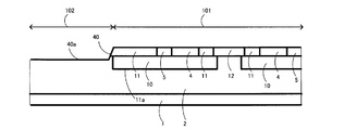
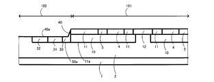
- the pressure-resistant structure portion 102 is provided with a stepped portion 40 that is disposed on the outer peripheral portion of the second p base region 11 and deeper than the bottom surface of the second p base region 11. Then, the second p base region 11 is covered with an interlayer insulating film 14 through a thick insulating film 13 from the outer periphery. A p region 33 disposed in the surface layer of the n-type silicon carbide epitaxial layer 2 is provided in the lower portion near the step portion 40 in contact with the second p base region 11 and the first p base region 10.
- the p region 33 is an electric field relaxation region that prevents a decrease in breakdown voltage at the stepped portion 40 and also functions as JTE. Further, the p regions 31 and 32 constitute a JTE (Junction Terminal Extension) of the breakdown voltage structure 102.
- the n-type silicon carbide substrate 1 is, for example, a silicon carbide single crystal substrate doped with nitrogen (N).
- N type silicon carbide epitaxial layer 2 is an n type drift layer (first n drift region) doped with nitrogen, for example, having an impurity concentration lower than that of n type silicon carbide substrate 1.
- the first p base region 10 is doped with, for example, aluminum so that its impurity concentration is 4 ⁇ 10 17 cm ⁇ 3 or more and 1 ⁇ 10 18 cm ⁇ 3 or less.
- the depth of the first p base region 10 is, for example, about 0.5 ⁇ m.
- the second p base region 11 is, for example, a p-type silicon carbide epitaxial layer 11a doped with aluminum, and has an impurity concentration of, for example, about 2 ⁇ 10 16 cm ⁇ 3 and a thickness of about 0.5 ⁇ m.
- Second n drift region 12 is a JFET region, and is formed by ion implantation of nitrogen into p type silicon carbide epitaxial layer 11a which is second p base region 11. The dose is adjusted so that the impurity concentration of the second n drift region 12 is, for example, about 5.0 ⁇ 10 16 cm ⁇ 3 .
- the thickness is, for example, about 0.6 ⁇ m.
- the impurity concentration of the n source region 4 is higher than that of the second n drift region 12, and is, for example, about 1 ⁇ 10 20 cm ⁇ 3 .
- the thickness of the gate insulating film 6 is, for example, about 100 nm.
- the interlayer insulating film 14 is a phosphor glass film and has a thickness of, for example, 1.0 ⁇ m.
- the source electrode 8 is an aluminum (Al—Si) film containing silicon at a rate of about 1%, for example, and the thickness thereof is, for example, about 5 ⁇ m.
- the drain electrode 9 that is the back electrode is, for example, a laminated film of titanium, nickel, and gold (Au).
- Silicon carbide semiconductor device 100 is provided with a stepped portion 40 that is disposed on the outer periphery of second p base region 11 and deeper than the bottom surface of second p base region 11.
- the depth of the stepped portion 40 is about 0.4 ⁇ m to 0.7 ⁇ m, which is about 0.1 ⁇ m deeper than the depth of the second p base region 11.
- a p region 33 that is an electric field relaxation region is provided in the vicinity of the stepped portion 40.
- the impurity concentration of the p region 33 is lower than that of the first p base region 10 and higher than that of the p regions 31 and 32 constituting the breakdown voltage structure 102.
- a preferable impurity concentration range of the p region 33 is preferably 2 ⁇ 10 16 cm ⁇ 3 to 1 ⁇ 10 17 cm ⁇ 3 .
- the p regions 31 and 32 preferably have an impurity concentration lower than that of the adjacent p region 33, and preferably 1 ⁇ 10 16 cm ⁇ 3 to 9 ⁇ 10 16 cm ⁇ 3 .
- the purpose of making the stepped portion 40 deeper than the depth of the second p base region 11 and shallower than the depth of the first p base region 10 is to expose the p regions 31 and 32 serving as JTE on the bottom surface 40 a of the stepped portion 40.
- the first p base region 10 is connected substantially flatly from the bottom surface 10a of the first p base region 10 to the bottom surfaces of the p regions 31 and 32 via the bottom surface 33a of the p region 33.
- the difference between the bottom surfaces may be within ⁇ 0.1 ⁇ m.
- the bottom surface from the p region 33 to the p regions 31 and 32 and the bottom surface of the first p base region 10 disposed in the active region are substantially flattened, and the impurity concentration of the p region 33 is made lower than that of the first p base region 10. .
- the breakdown voltage of the breakdown voltage structure 102 can be made higher than the breakdown voltage of the active region 101, so that an avalanche always occurs in the first p base region 10.
- the first p base region 10 tends to have a larger avalanche resistance compared to the p regions 31, 32, 33 due to its larger area. For this reason, there is an effect that the avalanche resistance can be increased by designing the first p base region 10 to break.
- the breakdown voltage drop in the breakdown voltage structure 102 is suppressed, for example, 1200 V High breakdown voltage silicon carbide semiconductor device 100 of the breakdown voltage class can be manufactured.
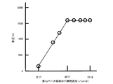
- FIG. 2 is a diagram showing the relationship between the impurity concentration of the first p base region and the breakdown voltage of the silicon carbide semiconductor device.
- the vertical axis represents the breakdown voltage
- the horizontal axis represents the impurity concentration of the first p base region.
- the depth of the stepped portion 40 is 0.6 ⁇ m
- the impurity concentration of the p region 33 is 1 ⁇ 10 17 cm ⁇ 3
- the conditions such as planarization of the bottom surfaces of the p region 33 and the first p base region 10 are satisfied, and the first p base
- the impurity concentration of the region 10 is 4 ⁇ 10 17 cm ⁇ 3 or more and 1 ⁇ 10 18 cm ⁇ 3 or less
- avalanche in the breakdown voltage structure portion 102 is suppressed, and a high breakdown voltage exceeding 1600 V can be obtained.
- high breakdown voltage silicon carbide semiconductor device 100 can be manufactured.
- 3 to 15 are main part manufacturing step sectional views showing the manufacturing method of silicon carbide semiconductor device 100 according to the second embodiment of the present invention in the order of steps.
- a first layer having a thickness of about 10 ⁇ m is doped on the (000-1) plane of the n-type silicon carbide substrate 1 with an impurity concentration of about 1.0 ⁇ 10 16 cm ⁇ 3 , for example.
- N-type silicon carbide epitaxial layer 2 to be a 1n drift region is grown.
- the p regions 31 and 32 of the breakdown voltage structure 102 and the first p base region 10 and the p region 31 of the active region 101 are formed on the surface layer of the n-type silicon carbide epitaxial layer 2 by photolithography and ion implantation. And a first p base region 10 are selectively formed in contact with the p region 33 to be an electric field relaxation region.
- the dopant is aluminum, and the dose is set so that the impurity concentration of the first p base region 10 is, for example, about 1.0 ⁇ 10 18 cm ⁇ 3 .
- the impurity concentration of the p regions 31 and 32 is, for example, 1 ⁇ 10 16 cm ⁇ 3 to 9 ⁇ 10 16 cm ⁇ 3, and the impurity concentration of the p region 33 is between the first p base region 10 and the p regions 31 and 32.
- the range is from 2 ⁇ 10 16 cm ⁇ 3 to 1 ⁇ 10 17 cm ⁇ 3 .
- the depth of the first p base region 10 is about 0.5 ⁇ m.
- a p-type silicon carbide epitaxial layer 11a to be the second p base region 11 is formed on the surface of the n-type silicon carbide epitaxial layer 2 in which the first p base region 10 is formed with a thickness of about 0.5 ⁇ m, for example.
- the growth is performed with an impurity concentration of about 2.0 ⁇ 10 16 cm ⁇ 3 .
- the conductivity type of the p-type silicon carbide epitaxial layer 11a on the n-type silicon carbide epitaxial layer 2 sandwiched between the first p base regions 10 by photolithography and ion implantation and the heat treatment shown in FIG. are inverted to selectively form the second n drift region 12.
- the dopant is nitrogen
- the dose is set so that the impurity concentration of the second n drift region 12 is about 5.0 ⁇ 10 16 cm ⁇ 3 .
- the depth of the second n drift region 12 is, for example, about 0.6 ⁇ m.
- the p-type silicon carbide epitaxial layer 11a includes the second p base region 11, the p contact region 5, the n source region 4, the second p base region 11, and the second n
- the drift region 12, the second p base region 11, the n source region 4, the p contact region 5, and the second p base region 11 are repeatedly formed in contact with each other.
- p-type silicon carbide epitaxial layer 11 a (p base region 11) is formed at a depth reaching p regions 31 and 32 to be breakdown voltage structure portion 102 and part of p region 33 that is an electric field relaxation region.
- the etching depth is, for example, about 0.4 to 0.7 ⁇ m.
- the n source region 4, the p contact region 5, the second n drift region 12, the first p base region 10, the p regions 31 and 32 of the breakdown voltage structure 102, and the p region 33 that is an electric field relaxation region are simultaneously formed.
- Heat treatment (annealing) for activation is performed.
- the heat treatment temperature and heat treatment time at this time are, for example, about 1620 ° C. and about 2 minutes, respectively.
- the order in which the n source region 4, the p contact region 5, and the second n drift region 12 are formed can be variously changed. Each region is formed by this collective heat treatment.
- the surface of the p-type silicon carbide epitaxial layer 11a on which the second p base region 11, the n source region 4, the p contact region 5, and the second n drift region 12 are formed is thermally oxidized to form a gate insulating film.
- 6 gate oxide film
- This thermal oxidation is performed by heat treatment at a temperature of about 1000 ° C. in a mixed atmosphere of oxygen and hydrogen. Thereby, each region is covered with the gate insulating film 6. At this time, the insulating film 13 is also formed.
- a polycrystalline silicon layer doped with, for example, phosphorus (P) is formed on the gate insulating film 6. Subsequently, the polycrystalline silicon layer is patterned and selectively removed to form the gate electrode 7.
- phosphorous glass PSG: Phosphosilicate Glass
- the interlayer insulating film 14 and the gate insulating film 6 are patterned and selectively removed to form a contact hole 14a, and the n source region 4 and the p contact region 5 are exposed.
- heat treatment for planarizing the interlayer insulating film 14 is performed.
- the source electrode 8 is selectively formed by photolithography.
- a nickel film is selectively formed in the contact hole as a contact electrode (not shown), and then heat-treated at a temperature of about 970 ° C., for example, to form the n source region 4 and the p contact region 5 and the contact electrode.
- An ohmic junction is formed.
- the source electrode 8 is embedded, and the contact electrode and the source electrode 8 are brought into contact with each other.
- the source electrode 8 is formed of aluminum containing silicon (Al—Si) at a rate of, for example, about 1% after the back surface contact annealing, and the thickness thereof is, for example, about 5 ⁇ m.
- FIGS. 16 to 21 are cross-sectional views showing a main part manufacturing process showing the silicon carbide semiconductor device 100 according to the third embodiment of the present invention in the order of the processes.
- the step region 40 is formed at the end of the first p base region 10 and then the p region 33 to be an electric field relaxation region is formed.
- the bottom surface 10a of the first p base region and the bottom surface 33a of the p region 33 are connected substantially flat.
- the first p base region 10 of the active region 101 is formed on the surface layer of the n-type silicon carbide epitaxial layer 2 by photolithography and ion implantation and the heat treatment shown in FIG.
- a p-type silicon carbide epitaxial layer 11 a to be the second p base region 11 is formed on the surface of the n-type silicon carbide epitaxial layer 2 in which the first p base region 10 is formed.
- the conductivity type of the p-type silicon carbide epitaxial layer 11a on the n-type silicon carbide epitaxial layer 2 sandwiched between the first p base regions 10 by photolithography and ion implantation and the heat treatment shown in FIG. are inverted to selectively form the second n drift region 12.
- n source region 4 is selectively formed apart from second n drift region 12 in p type silicon carbide epitaxial layer 11 a by photolithography and ion implantation and heat treatment in the step of FIG. 21.
- the p contact region 5 is selectively formed in contact with the n source region 4 by photolithography and ion implantation.
- the p-type silicon carbide epitaxial layer 11 a in which these regions are not formed becomes the second p base region 11.
- the p-type silicon carbide epitaxial layer 11a includes the second p base region 11, the p contact region 5, the n source region 4, the second p base region 11, and the second n
- the drift region 12, the second p base region 11, the n source region 4, the p contact region 5, and the second p base region 11 are repeatedly formed in contact with each other.
- the stepped portion 40 is formed by etching the p-type silicon carbide epitaxial layer 11a (second p base region 11) from the end of the first p base region 10 toward the outer periphery.
- p regions 31 and 32 to be the breakdown voltage structure portion 102 are formed under the bottom surface 40 a of the step portion 40 by photolithography, ion implantation, and heat treatment, and the p region 31 and the first p base region 10 are formed.
- a p region 33 which is an electric field relaxation region to be connected is formed.
- the bottom surface 10a of the first p base region 10 and the bottom surface 33a of the p region 33 are connected substantially flat.
- the bottom surface 10a of the first p base region 10 and the bottom surface 33a of the p region 33 can be connected substantially flat by changing the acceleration voltage to the tapered surface of the stepped portion 40 and implanting ions.
Landscapes
- Electrodes Of Semiconductors (AREA)
- Recrystallisation Techniques (AREA)
Abstract
耐圧構造部での耐圧低下を防止した炭化珪素半導体装置およびその製造方法を提供する。p領域31,32と第1pベース領域10に接続する電界緩和領域であるp領域33を段差部40下に配置し、p領域31,32,33と第1pベース領域10のそれぞれの底面を略平坦に接続する。第1ベース領域の不純物濃度は4×1017cm-3以上とし、p領域33の不純物濃度を第1ベース領域10より低く、且つp領域31,32よりも高い値に設定することで、耐圧構造部102での耐圧低下を防止できる。
Description
この発明は、ワイドバンドギャップ基板を用いて形成された炭化珪素半導体装置およびその製造方法に関する。
従来、高電圧や大電流を制御するパワー半導体装置の構成材料として、シリコン(Si)が用いられている。パワー半導体装置は、バイポーラトランジスタやIGBT(絶縁ゲート型バイポーラトランジスタ)、MOSFET(絶縁ゲート型電界効果トランジスタ)など複数種類あり、これらは用途に合わせて使い分けられている。
例えば、バイポーラトランジスタやIGBTは、MOSFETに比べて電流密度は高く大電流化が可能であるが、高速スイッチング動作ができない。具体的には、バイポーラトランジスタは数kHz程度のスイッチング周波数での使用が限界であり、IGBTは数十kHz程度のスイッチング周波数での使用が限界である。一方、パワーMOSFETは、バイポーラトランジスタやIGBTに比べて電流密度が低く大電流化が難しいが、数MHz程度までの高速スイッチング動作が可能である。
市場では大電流と高速性とを兼ね備えたパワー半導体装置への要求が強い。このため、IGBTやパワーMOSFETはその改良に力が注がれ、現在ではシリコンの材料限界に近いところまで開発が進んでいる。そこで、低オン電圧、高速特性、高温特性に優れた次世代のパワー半導体装置を作製(製造)可能な半導体材料として炭化珪素(SiC)が注目を集めている(例えば、非特許文献1)。
炭化珪素は、化学的に非常に安定した半導体材料であり、バンドギャップが3eVと広く、高温でも半導体として極めて安定的に使用することができる。また、炭化珪素は、最大電界強度がシリコンより1桁以上大きいため、高耐圧化と低オン抵抗を図ることができる半導体材料として期待される。このような炭化珪素の特長は、バンドギャップが広い半導体(以下、ワイドバンドギャップ半導体とする)である、例えば窒化ガリウム(GaN)にもあてはまる。このように、ワイドバンドギャップ半導体を用いることにより、高耐圧化を図った半導体装置が開示されている(例えば、非特許文献2)。
高耐圧半導体装置では、素子構造が形成された活性領域だけでなく、活性領域の周辺部に設けられ耐圧を保持する耐圧構造部にも高電圧が印加され、耐圧構造部に電界が集中する。高耐圧半導体装置の耐圧は、半導体の不純物濃度、厚さおよび電界強度によって決定され、このように半導体固有の特長によって決定される破壊耐量は活性領域から耐圧構造部にわたって等しい。このため、耐圧構造部に電界が集中することにより、耐圧構造部に破壊耐量を超えた電気的負荷がかかり破壊に至る虞がある。
耐圧構造部の電界を緩和または分散させることで耐圧を向上させた高耐圧半導体装置として、接合終端(JTE:Junction Termination Extension)構造や、フローティングリミッティングリング(FLR:Floating field Limiting Ring)構造などの終端構造を耐圧構造部に形成した半導体装置が開示されている。また、FLRに接するフローティングの金属電極をフィールドプレート(FP:Field Plate)として配置し、耐圧構造部に生じた電荷を放出させることにより信頼性の向上を図った半導体装置が開示されている(例えば、特許文献1,2)。
図22は、従来の炭化珪素半導体装置200の要部断面図である。この炭化珪素半導体装置200は、スイッチングデバイスであるNチャネルのMOSFETを例に挙げた。以下の説明において、炭化珪素をSiCと称すこともある。
図22は、従来の炭化珪素半導体装置200の要部断面図である。この炭化珪素半導体装置200は、スイッチングデバイスであるNチャネルのMOSFETを例に挙げた。以下の説明において、炭化珪素をSiCと称すこともある。
この炭化珪素半導体装置200は、n型SiC基板51の表面に配置されるn型SiC層52と、そのn型SiC層52表面に配置される複数のp型領域60と、p型領域60上に配置されるp型SiC層61を備える。更にp型領域60が形成されていないn型SiC層52上のp型SiC層61に配置されるJFET(接合型電界効果トランジスタ)領域となるn型領域62と、p型SiC層61の表面に配置されるn型ソース領域54とp型コンタクト領域55を備える。n型ソース領域54とp型コンタクト領域55との表面に配置されるソース電極58を備える。
またn型ソース領域54とn型領域62に挟まれたp型SiC層61の表面にゲート絶縁膜56を介して配置されるゲート電極57と、n型SiC基板51の裏面側に配置されるドレイン電極59を備える。
この炭化珪素半導体装置200において、ソース電極58に対しドレイン電極59に正の電圧が印加された状態でゲート電極57にゲート閾値以下の電圧が印加される場合には、p型領域60とn型SiC層52或いはp型SiC層61とn型領域62の間のpn接合が逆バイアスされた状態であり、活性領域201の耐圧が確保されて電流は流れない。
一方、ゲート電極57にゲート閾値以上の電圧を印加すると、ゲート電極57直下のp型SiC層61の表面には反転層(nチャネル)が形成されて電流が流れる。ゲート電極57に印加する電圧によって炭化珪素半導体装置200がスイッチング動作を行うことができる。
この炭化珪素半導体装置200の耐圧構造部202は、p型SiC層61の外周部が除去されている分だけ基板が薄くなっており、この基板の薄い部分にp領域81、82を備える。高電圧が印加された際、活性領域201以外での横方向での高電圧はこのp領域81、82とn型SiC層52の接合部分で維持する。尚、耐圧構造部202は、段差部90より外周部に配置される。
ケイ・シェナイ(K.Shenai)、外2名、オプティミウムセミコンダクターズ フォー ハイパワー エレクトロニクス(Optimum Semiconductors for High-Power Electronics)、アイ・トリプル・イー トランザクションズ オン エレクトロン デバイシズ(IEEE Transactions on Electron Devices)、1989年9月、第36巻、第9号、p.1811-1823
ビー・ジャヤン・バリガ(B.Jayant Baliga)著、シリコンカーバイド パワー デバイシズ(Silicon Carbide Power Divices)、(米国)、ワールド パブリッシング カンパニー(WorldScientific Publishing Co.)、2006年3月30日、p.61
しかし、図22に示す炭化珪素半導体装置200において、ドレイン電極59に高電圧が印加された場合、p型領域60の不純物濃度が低くなると、段差部を挟んでp領域81,82とp型領域60の電界分担が異なり、段差部90で耐圧の低下を招く。また、p型SiC層61をエッチングする際に発生する段差部90の形状とp領域81,82の表面での不純物濃度のばらつきによって耐圧の低下を招く。
また、図22に示すようにp型領域60の底面よりp領域81,82の底面が深い場合には、p領域81,82下のn型SiC層52の厚さが薄くなるので、p領域81、82でアバランシェが起こり易くなり、活性領域201より耐圧構造部202での耐圧は低下する。また、活性領域201に比べて耐圧構造部202の面積は小さいため、アバランシェによる電流密度が過大になり、アバランシェ破壊が起こり易い。
また、特許文献1、2の構造では、段差部下のnドリフト層の幅が狭いために、活性領域ではなく段差部を含む耐圧構造部でアバランシェが起こり易く耐圧低下を招くものと推察される。
この発明の目的は、前記の課題を解決して、耐圧構造部での耐圧低下を防止した炭化珪素半導体装置およびその製造方法を提供することにある。
(発明の一般的開示)炭化珪素半導体装置は、第1導電型の炭化珪素基板を備えてよい。炭化珪素半導体装置は、第1炭化珪素エピタキシャル層を備えてよい。第1炭化珪素エピタキシャル層は、炭化珪素基板の表面に配置され炭化珪素基板より低濃度の第1導電型の第1ドリフト領域となってよい。炭化珪素半導体装置は、複数の第2導電型の第1ベース領域を備えてよい。複数の第2導電型の第1ベース領域は、第1炭化珪素エピタキシャル層の表面層に配置されてよい。炭化珪素半導体装置は、第2導電型の第2ベース領域を備えてよく、第1導電型のソース領域を備えてもよく、第2導電型のコンタクト領域を備えてもよい。第2導電型の第2ベース領域、第1導電型のソース領域および第2導電型のコンタクト領域は、第1ベース領域上に配置されてよい。第2導電型のコンタクト領域は、第2ベース領域より高濃度であってよい。炭化珪素半導体装置は、第1導電型の第2ドリフト領域を備えてよい。第1導電型の第2ドリフト領域は、第1ベース領域に挟まれた第1炭化珪素エピタキシャル層上に第2ベース領域に挟まれて配置されてよい。炭化珪素半導体装置は、ゲート電極を備えてよい。ゲート電極は、ソース領域と第2ドリフト領域に挟まれた第2ベース領域上にゲート絶縁膜を介して配置されてよい。炭化珪素半導体装置は、ソース電極を備えてよい。ソース電極は、ソース領域とコンタクト領域に電気的に接続してよい。炭化珪素半導体装置は、ドレイン電極を備えてよい。ドレイン電極は、炭化珪素基板に電気的に接続してよい。炭化珪素半導体装置は、段差部を備えてよい。段差部は、第2ベース領域の外周部に配置され第2ベース領域の底面より深く第1ベース領域の底面より浅くてよい。炭化珪素半導体装置は、第2導電型の第1半導体領域(p領域33)を備えてよい。第2導電型の第1半導体領域(p領域33)は、第1炭化珪素エピタキシャル層の表面層に配置され、段差部と第2ベース領域と第1ベース領域に接してよい。炭化珪素半導体装置は、第2導電型の第2半導体領域(p領域31)を備えてよい。第2導電型の第2半導体領域(p領域31)は、段差部の底面下の第1炭化珪素エピタキシャル層の表面層に配置され第1半導体領域に接してよい。炭化珪素半導体装置は、第2導電型の第3半導体領域(p領域32)を備えてよい。第2導電型の第3半導体領域(p領域32)は、段差部の底面下の第1炭化珪素エピタキシャル層の表面層に配置され第2半導体領域に接してよい。第1半導体領域の底面と第1ベース領域の底面は略平坦に接続されていてよい。第1半導体領域、第2半導体領域および3半導体領域の不純物濃度は第1ベース領域より低くてよい。第1半導体領域の不純物濃度は第2半導体領域および第3半導体領域の不純物濃度より高くてよい。第1ベース領域の不純物濃度は4×1017cm-3以上1×1018cm-3以下であってよい。
第1ベース領域、第1半導体領域、第2半導体領域、および3半導体領域、それぞれの底面の差は±0.1μm以内であってよい。第1半導体領域の不純物濃度が2×1016cm-3以上1×1017cm-3以下であってよい。第2半導体領域および第3半導体領域の不純物濃度が1×1016cm-3以上9×1016cm-3以下であってよい。
炭化珪素半導体装置の製造方法は、複数の第2導電型の第1ベース領域、第2導電型の第1半導体領域、第2導電型の第2半導体領域および第2導電型の第3半導体領域を互いに接するように形成する工程を有してよい。当該工程において、第1ドリフト領域となる第1導電型の第1炭化珪素エピタキシャル層の表面層に選択的にイオン注入してよい。炭化珪素半導体装置の製造方法は、第1半導体領域の底面と第1ベース領域の底面を略平坦に接続して形成する工程を有してよい。炭化珪素半導体装置の製造方法は、第1炭化珪素エピタキシャル層上に第2導電型の第2炭化珪素エピタキシャル層を形成する工程を有してよい。炭化珪素半導体装置の製造方法は、第1導電型のソース領域、第2導電型のコンタクト領域を形成する工程を有してよい。当該工程において、第1ベース領域上の第2炭化珪素エピタキシャル層に選択的にイオン注入してよい。炭化珪素半導体装置の製造方法は、第1導電型の第2ドリフト領域を形成する工程を有してよい。当該工程において、第1ベース領域に挟まれた第1炭化珪素エピタキシャル層上の第2炭化珪素エピタキシャル層にイオン注入してよい。炭化珪素半導体装置の製造方法は、イオン注入されない個所を第2ベース領域とする工程を有してよい。炭化珪素半導体装置の製造方法は、前記第1半導体領域から、前記第2半導体領域、第3半導体領域および外周部の前記第1炭化珪素エピタキシャル層の上に形成された前記第2炭化珪素エピタキシャル層をエッチングで除去する工程を有してよい。炭化珪素半導体装置の製造方法は、段差部を第1半導体領域の位置に形成する工程を有してよい。段差部は、第2炭化珪素エピタキシャル層の底面より深く、第1ベース領域の底面より浅くてよい。第1半導体領域、第2半導体領域および第3半導体領域の不純物濃度は第1ベース領域の不純物濃度より低くてよい。第1半導体領域の不純物濃度は第2半導体領域および第3半導体領域の不純物濃度より高くてよい。第1ベース領域の不純物濃度を4×1017cm-3以上1×1018cm-3以下にしてよい。
炭化珪素半導体装置の製造方法は、複数の第2導電型の第1ベース領域と、第1ベース領域と離して第2導電型の第2半導体領域および第2半導体領域に隣接した第2導電型の第3半導体領域を形成する工程を有してよい。当該工程において、第1ドリフト領域となる第1導電型の第1炭化珪素エピタキシャル層の表面層に選択的にイオン注入してよい。炭化珪素半導体装置の製造方法は、第1炭化珪素エピタキシャル層上に第2導電型の第2炭化珪素エピタキシャル層を形成する工程を有してよい。炭化珪素半導体装置の製造方法は、第1導電型のソース領域、第2導電型のコンタクト領域を形成する工程を有してよい。当該工程において、第1ベース領域上の第2炭化珪素エピタキシャル層に選択的にイオン注入してよい。炭化珪素半導体装置の製造方法は、第1導電型の第2ドリフト領域を形成する工程を有してよい。当該工程において、第1ベース領域に挟まれた第1炭化珪素エピタキシャル層上の第2炭化珪素エピタキシャル層にイオン注入してよい。炭化珪素半導体装置の製造方法は、イオン注入されない個所を第2ベース領域とする工程を有してよい。炭化珪素半導体装置の製造方法は、第1ベース領域の端部より外周側の第2炭化珪素エピタキシャル層をエッチングで除去する工程を有してよい。炭化珪素半導体装置の製造方法は、段差部を第1ベースと第2半導体領域との間に形成する工程を有してよい。当該工程において、段差部は、第2炭化珪素エピタキシャル層の底面より深く第1ベース領域の底面より浅くてよい。炭化珪素半導体装置の製造方法は、第1半導体領域を形成する工程を有してよい。当該工程において、第1半導体領域は、段差部下の第1炭化珪素エピタキシャル層の表面層に、第1ベース領域、第2ベース領域および第2半導体領域に接続してよい。第1半導体領域は、第1ベース領域の底部と略平坦に接続してよい。第1半導体領域、第2半導体領域および第3半導体領域の不純物濃度は第1ベース領域の不純物濃度より低くてよい。第1半導体領域の不純物濃度は第2半導体領域および第3半導体領域の不純物濃度より高くてよい。第1ベース領域の不純物濃度は4×1017cm-3以上1×1018cm-3以下であってよい。
この発明により、耐圧構造部での耐圧低下を防止した炭化珪素半導体装置およびその製造方法を提供することができる。
以下の実施の形態では、第1導電型をn型、第2導電型をp型とした。勿論、これと逆の場合もある。なお、本明細書において、n型炭化珪素基板1の基板平面に垂直な方向であって、ドレイン電極9から保護膜15に向かう方向を「上」と称する。「上」と逆の方向を「下」と称する。また、表面とは、基板、層、領域、電極および膜における上側の面を意味する。またさらに、裏面とは、基板、層、領域、電極および膜における下側の面を意味する。
(実施の形態1)
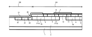
図1は、この発明の実施の形態1に係る炭化珪素半導体装置100の要部断面図である。ここでは炭化珪素半導体装置100として、縦型プレーナゲート構造のMOSFETを例に挙げた。
(実施の形態1)
図1は、この発明の実施の形態1に係る炭化珪素半導体装置100の要部断面図である。ここでは炭化珪素半導体装置100として、縦型プレーナゲート構造のMOSFETを例に挙げた。
この炭化珪素半導体装置100は、nドレイン層となる高濃度のn型炭化珪素基板1と、n炭化珪素基板1の表面に配置されn型炭化珪素基板1より低濃度の第1nドリフト領域となるn型炭化珪素エピタキシャル層2と、n型炭化珪素エピタキシャル層2の表面層に配置されイオン注入で形成される高濃度である第1pベース領域10を備える。また、第1pベース領域10上に配置される第2pベース領域11、nソース領域4、pコンタクト領域5、第2nドリフト領域12を備える。nソース領域4と第2nドリフト領域12に挟まれた第2pベース領域11上にゲート絶縁膜6を介して配置されるゲート電極7を備える。ゲート電極7上に配置される層間絶縁膜14と、層間絶縁膜14上に配置されnソース領域4およびpコンタクト領域5に接続するソース電極8と、最表面を被覆する表面保護膜15を備える。
耐圧構造部102には、第2pベース領域11の外周部に配置され第2pベース領域11の底面より深い段差部40が設けられる。そして、第2pベース領域11から外周部にかけて、厚い絶縁膜13を介して層間絶縁膜14で覆われている。段差部40付近の下部には、前記第2pベース領域11と第1pベース領域10に接してn型炭化珪素エピタキシャル層2の表面層に配置されるp領域33を備える。p領域33に接して段差部40の底面40a下に配置されるp領域31と、p領域31に隣接して底面40a下に配置されるp領域32を備える。p領域33は、段差部40での耐圧低下を防止するとともに、JTEとしても機能する電界緩和領域である。また、p領域31,32は耐圧構造部102のJTE(Junction Terminal Extension)を構成する。
前記のn型炭化珪素基板1は、例えば、窒素(N)がドーピングされた炭化珪素単結晶基板である。n型炭化珪素エピタキシャル層2は、n型炭化珪素基板1より不純物濃度が低く、例えば窒素がドーピングされたn型ドリフト層(第1nドリフト領域)である。前記の第1pベース領域10は、例えば、アルミニウムをドーピングし、その不純物濃度を4×1017cm-3以上1×1018cm-3以下にする。また、第1pベース領域10の深さは、例えば、0.5μm程度である。第2pベース領域11は、例えば、アルミニウムがドーピングされたp型炭化珪素エピタキシャル層11aであり、その不純物濃度は、例えば、2×1016cm-3程度、厚さは0.5μm程度である。第2nドリフト領域12はJFET領域であり、第2pベース領域11であるp型炭化珪素エピタキシャル層11aに窒素をイオン注入して形成する。第2nドリフト領域12の不純物濃度は、例えば、5.0×1016cm-3程度になるようにドーズ量を調整する。その厚さは、例えば、0.6μm程度である。nソース領域4の不純物濃度は第2nドリフト領域12より高く、例えば、1×1020cm-3程度である。ゲート絶縁膜6の厚みは、例えば、100nm程度である。層間絶縁膜14はリンガラス膜であり、その厚さは、例えば、1.0μmである。ソース電極8は、例えば、1%程度の割合でシリコンを含んだアルミニウム(Al-Si)膜であり、その厚さは、例えば、5μm程度である。裏面電極であるドレイン電極9は例えば、チタン、ニッケルおよび金(Au)の積層膜である。
この炭化珪素半導体装置100は、第2pベース領域11の外周部に配置され第2pベース領域11の底面より深い段差部40を設ける。例えば、この段差部40の深さは0.4μm~0.7μm程度であり、第2pベース領域11の深さより0.1μm程度深い。そして、この段差部40近傍に電界緩和領域であるp領域33を設ける。p領域33の不純物濃度は第1pベース領域10より低くし、耐圧構造部102を構成するp領域31,32より高くする。具体的には、p領域33の好適な不純物濃度範囲は2×1016cm-3~1×1017cm-3であることが好ましい。またp領域31,32は、隣接するp領域33よりも不純物濃度が低いことが好ましく、好適には1×1016cm-3~9×1016cm-3が好ましい。段差部40を第2pベース領域11の深さより深く第1pベース領域10の深さより浅くする目的は、段差部40の底面40aにJTEとなるp領域31,32を露出させるためである。
さらに、第1pベース領域10の底面10aから前記のp領域33の底面33aを経由してp領域31,32の底面にかけて略平坦に接続する。ここで、略平坦とするためには、それぞれの底面の差を±0.1μm以内とすれば良い。このように、p領域33からp領域31,32にかけての底面と活性領域に配置される第1pベース領域10の底面を略平坦化し、p領域33の不純物濃度を第1pベース領域10より低くする。これにより、耐圧構造部102の耐圧を活性領域101の耐圧よりも高くできるので、アバランシェが必ず第1pベース領域10で発生するようになる。一般に、第1pベース領域10はp領域31,32,33と比較して面積が広い分だけアバランシェ耐量が大きい傾向がある。このため、第1pベース領域10で破壊するように設計することで、アバランシェ耐量を大きくすることができるという効果を奏する。また、この第1pベース領域10の不純物濃度を4×1017cm-3以上、1×1018cm-3以下とすることで、耐圧構造部102での耐圧低下は抑制されて、例えば、1200V耐圧クラスの高耐圧の炭化珪素半導体装置100を製作することができる。
図2は、第1pベース領域の不純物濃度と炭化珪素半導体装置の耐圧の関係を示す図である。縦軸は耐圧であり、横軸は第1pベース領域の不純物濃度である。段差部40の深さを0.6μm、p領域33の不純物濃度を1×1017cm-3、p領域33と第1pベース領域10の底面の平坦化などの条件を満たして、第1pベース領域10の不純物濃度を4×1017cm-3以上1×1018cm-3以下にすることで、耐圧構造部102でのアバランシェが抑制されて、1600V超の高い耐圧を得ることができる。その結果、高耐圧の炭化珪素半導体装置100を製作することができる。
(実施の形態2)
図3~図15は、この発明の実施の形態2に係る炭化珪素半導体装置100の製造方法について、工程順に示した要部製造工程断面図である。
(実施の形態2)
図3~図15は、この発明の実施の形態2に係る炭化珪素半導体装置100の製造方法について、工程順に示した要部製造工程断面図である。
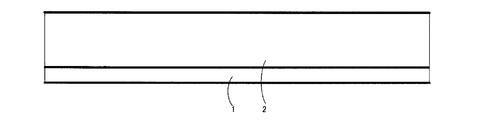
まず、図3において、例えば2×1019cm-3程度の不純物濃度で窒素がドーピングされたn型炭化珪素基板1を用意する。n型炭化珪素基板1は、主面が例えば<11-20>方向に4度程度のオフ角を有する(1000-1)面であってもよい。
次に、図4において、n型炭化珪素基板1の(000-1)面上に、例えば、1.0×1016cm-3程度の不純物濃度で窒素がドーピングされた厚さ10μm程度の第1nドリフト領域となるn型炭化珪素エピタキシャル層2を成長させる。
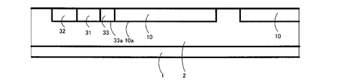
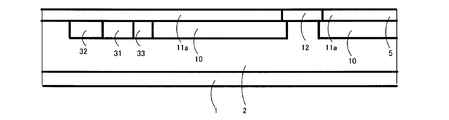
次に、図5において、フォトリソグラフィおよびイオン注入によって、n型炭化珪素エピタキシャル層2の表面層に、耐圧構造部102のp領域31,32と活性領域101の第1pベース領域10とp領域31と第1pベース領域10の間にそれぞれに接して電界緩和領域となるp領域33を選択的に形成する。このイオン注入では、例えば、ドーパントをアルミニウムとし、第1pベース領域10の不純物濃度が、例えば、1.0×1018cm-3程度となるようにドーズ量を設定する。p領域31、32の不純物濃度は、例えば、1×1016cm-3~9×1016cm-3とし、p領域33の不純物濃度は第1pベース領域10とp領域31,32の間で、2×1016cm-3~1×1017cm-3の範囲にする。第1pベース領域10深さは、0.5μm程度である。
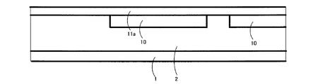
次に、図6において、第1pベース領域10が形成されたn型炭化珪素エピタキシャル層2の表面に、第2pベース領域11となるp型炭化珪素エピタキシャル層11aを、例えば0.5μm程度の厚さ、2.0×1016cm-3程度の不純物濃度で成長させる。
次に、図7において、フォトリソグラフィおよびイオン注入と図10に示す熱処理によって、第1pベース領域10で挟まれたn型炭化珪素エピタキシャル層2上の前記のp型炭化珪素エピタキシャル層11aの導電型を反転させて、第2nドリフト領域12を選択的に形成する。このイオン注入では、例えば、ドーパントを窒素とし、第2nドリフト領域12の不純物濃度が5.0×1016cm-3程度となるようにドーズ量を設定する。第2nドリフト領域12の深さは、例えば、0.6μm程度にする。
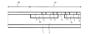
次に、図8において、フォトリソグラフィおよびイオン注入と図10の熱処理によって、pベース領域11となるp型炭化珪素エピタキシャル層11aに、第2nドリフト領域12と離してnソース領域4を選択的に形成する。続いて、フォトリソグラフィおよびイオン注入によって、nソース領域4に接してpコンタクト領域5を選択的に形成する。これによって、耐圧構造部102側から活性領域101に向かって、p型炭化珪素エピタキシャル層11aには、第2pベース領域11、pコンタクト領域5、nソース領域4、第2pベース領域11、第2nドリフト領域12、第2pベース領域11、nソース領域4、pコンタクト領域5、第2pベース領域11がそれぞれ接して繰り返して形成される。
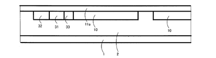
次に、図9において、耐圧構造部102となるp領域31,32および電界緩和領域であるp領域33の一部に達する深さで、p型炭化珪素エピタキシャル層11a(pベース領域11)をエッチングする。このエッチング深さは、例えば、0.4~0.7μm程度とする。このエッチングで活性領域101の表面高さより、耐圧構造部のp領域31,32および電界緩和領域のp領域33の一部の表面高さが低くなる。段差部40はp領域33の位置に形成され、p領域33は第1pベース領域10と第2pベース領域に接続する。
次に、図10において、nソース領域4、pコンタクト領域5、第2nドリフト領域12、第1pベース領域10、耐圧構造部102のp領域31,32および電界緩和領域であるp領域33を同時に活性化させるための熱処理(アニール)を行う。このときの熱処理温度および熱処理時間は、例えば、それぞれ1620℃程度および2分間程度である。nソース領域4、pコンタクト領域5および第2nドリフト領域12を形成する順序は種々変更可能である。尚、この一括熱処理によって各領域が形成される。
次に、図11において、第2pベース領域11、nソース領域4、pコンタクト領域5、第2nドリフト領域12が形成されているp型炭化珪エピタキシャル層11aの表面を熱酸化し、ゲート絶縁膜6(ゲート酸化膜)を100nm程度の厚さで形成する。この熱酸化は、酸素と水素の混合雰囲気中において1000℃程度の温度の熱処理によって行う。これにより、各領域はゲート絶縁膜6で覆われる。このとき、絶縁膜13も形成する。
次に、図12において、ゲート絶縁膜6上に、例えばリン(P)がドープされた多結晶シリコン層を形成する。続いて、多結晶シリコン層をパターニングして選択的に除去し、ゲート電極7を形成する。
次に、図13において、ゲート電極7を覆うように、層間絶縁膜14として例えばリンガラス(PSG:Phospho Silicate Glass)を1.0μm程度の厚さで成膜する。続いて、層間絶縁膜14およびゲート絶縁膜6をパターニングして選択的に除去してコンタクトホール14aを形成し、nソース領域4およびpコンタクト領域5を露出させる。続いて、層間絶縁膜14を平坦化するための熱処理(リフロー)を行う。
次に、図14において、フォトリソグラフィにより選択的にソース電極8を成膜する。はじめに、コンタクトホール内にコンタクト電極(不図示)として例えばニッケル膜を選択的に成膜し、そして、例えば970℃程度の温度で熱処理し、nソース領域4およびpコンタクト領域5とコンタクト電極とのオーミック接合を形成する。続いて、ソース電極8を埋め込み、コンタクト電極とソース電極8とを接触させる。ソース電極8は、裏面のコンタクトアニール後に、例えば、1%程度の割合でシリコンを含んだアルミニウム(Al-Si)で形成し、その厚さは、例えば5μm程度である。
次に、図15において、n型炭化珪素基板1の裏面に、コンタクト電極として例えばニッケル膜を成膜する。そして、例えば970℃程度の温度で熱処理し、n型炭化珪素基板1とコンタクト電極とのオーミック接合を形成する。続いて、コンタクト電極の裏面に、例えばチタン、ニッケルおよび金(Au)をこの順に成膜してドレイン電極9を形成する。続いて、ソース電極8を覆うように表面保護膜15を形成する。これにより、図1に示したMOSFETである炭化珪素半導体装置100が完成する。
(実施の形態3)
図16~図21は、この発明の実施の形態3に係る炭化珪素半導体装置100の製造方法について、工程順に示した要部製造工程断面図である。
(実施の形態3)
図16~図21は、この発明の実施の形態3に係る炭化珪素半導体装置100の製造方法について、工程順に示した要部製造工程断面図である。
実施の形態2との違いは、図5~図8の工程において、第1pベース領域10の端部に段差部40を形成した後に電界緩和領域となるp領域33を形成する点である。第1pベース領域の底面10aとp領域33の底面33aは略平坦に接続する。
前記した図4の工程の後に図16~図21の工程が続く。
図16において、フォトリソグラフィおよびイオン注入と図21に示す熱処理によって、n型炭化珪素エピタキシャル層2の表面層に、活性領域101の第1pベース領域10を形成する。
次に、図17において、第1pベース領域10が形成されたn型炭化珪素エピタキシャル層2の表面に、第2pベース領域11となるp型炭化珪素エピタキシャル層11aを形成する。
次に、図18において、フォトリソグラフィおよびイオン注入と図21に示す熱処理によって、第1pベース領域10で挟まれたn型炭化珪素エピタキシャル層2上の前記のp型炭化珪素エピタキシャル層11aの導電型を反転させて、第2nドリフト領域12を選択的に形成する。
次に、図19において、フォトリソグラフィおよびイオン注入と図21の工程の熱処理によって、p型炭化珪素エピタキシャル層11aに、第2nドリフト領域12と離してnソース領域4を選択的に形成する。続いて、フォトリソグラフィおよびイオン注入によって、nソース領域4に接してpコンタクト領域5を選択的に形成する。これらの領域が形成されないp型炭化珪素エピタキシャル層11aが第2pベース領域11になる。これによって、耐圧構造部102側から活性領域101に向かって、p型炭化珪素エピタキシャル層11aには、第2pベース領域11、pコンタクト領域5、nソース領域4、第2pベース領域11、第2nドリフト領域12、第2pベース領域11、nソース領域4、pコンタクト領域5、第2pベース領域11がそれぞれ接して繰り返して形成される。
次に、図20において、第1pベース領域10の端部より外周に向かって、p型炭化珪素エピタキシャル層11a(第2pベース領域11)をエッチングして段差部40を形成する。
次に、図21において、フォトリソグラフィおよびイオン注入と熱処理によって、段差部40の底面40a下に、耐圧構造部102となるp領域31,32を形成し、p領域31と第1pベース領域10に接続する電界緩和領域であるp領域33を形成する。このとき第1pベース領域10の底面10aとp領域33の底面33aを略平坦に接続する。例えば、段差部40のテーパー面に加速電圧を変化させてイオン注入することで、第1pベース領域10の底面10aとp領域33の底面33aを略平坦に接続することができる。
図21の工程の後に前記した図11~図15の工程に移行する。
1 n型炭化珪素基板
2 n型炭化珪素エピタキシャル層
4 nソース領域
5 pコンタクト領域
6 ゲート絶縁膜
7 ゲート電極
8 ソース電極
9 ドレイン電極
10 第1pベース領域
10a,33a,40a 底面
11 第2pベース領域
11a p型炭化珪素エピタキシャル層
12 第2nドリフト領域
13 絶縁膜
14 層間絶縁膜
15 保護膜
31,32 p領域(耐圧構造部101)
33 p領域(電界緩和領域)
40 段差部
51 n型SiC基板
52 n型SiC層
54 n型ソース領域
55 p型コンタクト領域
56 ゲート絶縁膜
57 ゲート電極
58 ソース電極
59 ドレイン電極
60 p型領域
61 p型SiC層
62 n型領域
81 p領域
82 p領域
90 段差部
100 炭化珪素半導体装置
101 活性領域
102 耐圧構造部
200 炭化珪素半導体装置
201 活性領域
202 耐圧構造部
2 n型炭化珪素エピタキシャル層
4 nソース領域
5 pコンタクト領域
6 ゲート絶縁膜
7 ゲート電極
8 ソース電極
9 ドレイン電極
10 第1pベース領域
10a,33a,40a 底面
11 第2pベース領域
11a p型炭化珪素エピタキシャル層
12 第2nドリフト領域
13 絶縁膜
14 層間絶縁膜
15 保護膜
31,32 p領域(耐圧構造部101)
33 p領域(電界緩和領域)
40 段差部
51 n型SiC基板
52 n型SiC層
54 n型ソース領域
55 p型コンタクト領域
56 ゲート絶縁膜
57 ゲート電極
58 ソース電極
59 ドレイン電極
60 p型領域
61 p型SiC層
62 n型領域
81 p領域
82 p領域
90 段差部
100 炭化珪素半導体装置
101 活性領域
102 耐圧構造部
200 炭化珪素半導体装置
201 活性領域
202 耐圧構造部
Claims (6)
- 第1導電型の炭化珪素基板と、前記炭化珪素基板の表面に配置され前記炭化珪素基板より低濃度の第1導電型の第1ドリフト領域となる第1炭化珪素エピタキシャル層と、前記第1炭化珪素エピタキシャル層の表面層に配置される複数の第2導電型の第1ベース領域と、
前記第1ベース領域上に配置される第2導電型の第2ベース領域、第1導電型のソース領域、および前記第2ベース領域より高濃度の第2導電型のコンタクト領域と、
前記第1ベース領域に挟まれた前記第1炭化珪素エピタキシャル層上に前記第2ベース領域に挟まれて配置される第1導電型の第2ドリフト領域と、
前記ソース領域と前記第2ドリフト領域に挟まれた前記第2ベース領域上にゲート絶縁膜を介して配置されるゲート電極と、前記ソース領域と前記コンタクト領域に電気的に接続するソース電極と、前記炭化珪素基板に電気的に接続するドレイン電極と、
前記第2ベース領域の外周部に配置され前記第2ベース領域の底面より深く前記第1ベース領域の底面より浅い段差部と、
前記第1炭化珪素エピタキシャル層の表面層に配置され、前記段差部と前記第2ベース領域と前記第1ベース領域とに接する第2導電型の第1半導体領域と、
前記段差部の底面下の前記第1炭化珪素エピタキシャル層の表面層に配置され前記第1半導体領域に接する第2導電型の第2半導体領域と、
前記段差部の底面下の前記第1炭化珪素エピタキシャル層の表面層に配置され前記第2半導体領域に接する第2導電型の第3半導体領域と、を備え、
前記第1半導体領域の底面と前記第1ベース領域の底面を略平坦に接続しており、前記第1半導体領域、前記第2半導体領域および前記3半導体領域の不純物濃度は前記第1ベース領域より低く、前記第1半導体領域の不純物濃度は前記第2半導体領域および前記第3半導体領域の不純物濃度より高く、前記第1ベース領域の不純物濃度は4×1017cm-3以上1×1018cm-3以下であることを特徴とする炭化珪素半導体装置。 - 前記第1ベース領域、前記第1半導体領域、前記第2半導体領域、および前記3半導体領域、それぞれの底面の差が±0.1μm以内であることを特徴とする請求項1に記載の炭化珪素半導体装置。
- 前記第1半導体領域の不純物濃度が2×1016cm-3以上1×1017cm-3以下であることを特徴とする請求項1に記載の炭化珪素半導体装置。
- 前記第2半導体領域および前記第3半導体領域の不純物濃度が1×1016cm-3以上9×1016cm-3以下であることを特徴とする請求項1に記載の炭化珪素半導体装置。
- 第1ドリフト領域となる第1導電型の第1炭化珪素エピタキシャル層の表面層に選択的にイオン注入し複数の第2導電型の第1ベース領域、第2導電型の第1半導体領域、第2導電型の第2半導体領域および第2導電型の第3半導体領域を互いに接するように形成し、さらに前記第1半導体領域の底面と前記第1ベース領域の底面を略平坦に接続して形成する工程と、
前記第1炭化珪素エピタキシャル層上に第2導電型の第2炭化珪素エピタキシャル層を形成する工程と、
前記第1ベース領域上の前記第2炭化珪素エピタキシャル層に選択的にイオン注入し第1導電型のソース領域、第2導電型のコンタクト領域を形成し、前記第1ベース領域に挟まれた前記第1炭化珪素エピタキシャル層上の前記第2炭化珪素エピタキシャル層にイオン注入により第1導電型の第2ドリフト領域を形成し、イオン注入されない個所を第2ベース領域とする工程と、
前記第1半導体領域から、前記第2半導体領域、第3半導体領域および外周部の前記第1炭化珪素エピタキシャル層の上に形成された前記第2炭化珪素エピタキシャル層をエッチングで除去し、前記第2炭化珪素エピタキシャル層の底面より深く、前記第1ベース領域の底面より浅い段差部を前記第1半導体領域の位置に形成する工程と
を含み、
前記第1半導体領域、前記第2半導体領域および前記第3半導体領域の不純物濃度が前記第1ベース領域の不純物濃度より低く、前記第1半導体領域の不純物濃度が前記第2半導体領域および前記第3半導体領域の不純物濃度より高く、前記第1ベース領域の不純物濃度が4×1017cm-3以上1×1018cm-3以下に設定することを特徴とする炭化珪素半導体装置の製造方法。 - 第1ドリフト領域となる第1導電型の第1炭化珪素エピタキシャル層の表面層に選択的にイオン注入し複数の第2導電型の第1ベース領域と、前記第1ベースと離して第2導電型の第2半導体領域および前記第2半導体領域に隣接した第2導電型の第3半導体領域を形成する工程と、
前記第1炭化珪素エピタキシャル層上に第2導電型の第2炭化珪素エピタキシャル層を形成する工程と、
前記第1ベース領域上の前記第2炭化珪素エピタキシャル層に選択的にイオン注入し第1導電型のソース領域、第2導電型のコンタクト領域を形成し、前記第1ベース領域に挟まれた前記第1炭化珪素エピタキシャル層上の前記第2炭化珪素エピタキシャル層にイオン注入により第1導電型の第2ドリフト領域を形成し、イオン注入されない個所を第2ベース領域とする工程と、
前記第1ベース領域の端部より外周側の前記第2炭化珪素エピタキシャル層をエッチングで除去し、前記第2炭化珪素エピタキシャル層の底面より深く前記第1ベース領域の底面より浅い段差部を前記第1ベースと前記第2半導体領域との間に形成する工程と、
前記段差部下の第1炭化珪素エピタキシャル層の表面層に、前記第1ベース領域、前記第2ベース領域および前記第2半導体領域に接続し、前記第1ベース領域の底部と略平坦に接続する第1半導体領域を形成する工程と
を含み、
前記第1半導体領域、前記第2半導体領域および前記第3半導体領域の不純物濃度が前記第1ベース領域の不純物濃度より低く、前記第1半導体領域の不純物濃度が前記第2半導体領域および前記第3半導体領域の不純物濃度より高く、前記第1ベース領域の不純物濃度が4×1017cm-3以上1×1018cm-3以下に設定することを特徴とする炭化珪素半導体装置の製造方法。
Priority Applications (2)
| Application Number | Priority Date | Filing Date | Title |
|---|---|---|---|
| JP2016554000A JP6265278B2 (ja) | 2014-10-15 | 2015-08-20 | 炭化珪素半導体装置およびその製造方法 |
| US15/279,450 US9905554B2 (en) | 2014-10-15 | 2016-09-29 | Silicon carbide semiconductor device and method of manufacturing the same |
Applications Claiming Priority (2)
| Application Number | Priority Date | Filing Date | Title |
|---|---|---|---|
| JP2014-210360 | 2014-10-15 | ||
| JP2014210360 | 2014-10-15 |
Related Child Applications (1)
| Application Number | Title | Priority Date | Filing Date |
|---|---|---|---|
| US15/279,450 Continuation-In-Part US9905554B2 (en) | 2014-10-15 | 2016-09-29 | Silicon carbide semiconductor device and method of manufacturing the same |
Publications (1)
| Publication Number | Publication Date |
|---|---|
| WO2016059871A1 true WO2016059871A1 (ja) | 2016-04-21 |
Family
ID=55746419
Family Applications (1)
| Application Number | Title | Priority Date | Filing Date |
|---|---|---|---|
| PCT/JP2015/073388 Ceased WO2016059871A1 (ja) | 2014-10-15 | 2015-08-20 | 炭化珪素半導体装置およびその製造方法 |
Country Status (3)
| Country | Link |
|---|---|
| US (1) | US9905554B2 (ja) |
| JP (1) | JP6265278B2 (ja) |
| WO (1) | WO2016059871A1 (ja) |
Citations (4)
| Publication number | Priority date | Publication date | Assignee | Title |
|---|---|---|---|---|
| JPH1174524A (ja) * | 1997-06-30 | 1999-03-16 | Denso Corp | 半導体装置及びその製造方法 |
| JPH11354791A (ja) * | 1998-06-12 | 1999-12-24 | Denso Corp | 炭化珪素半導体装置及びその製造方法 |
| JP2010147222A (ja) * | 2008-12-18 | 2010-07-01 | Denso Corp | 炭化珪素半導体装置およびその製造方法 |
| JP2013232564A (ja) * | 2012-04-27 | 2013-11-14 | National Institute Of Advanced Industrial & Technology | 半導体装置および半導体装置の製造方法 |
Family Cites Families (5)
| Publication number | Priority date | Publication date | Assignee | Title |
|---|---|---|---|---|
| US6054752A (en) | 1997-06-30 | 2000-04-25 | Denso Corporation | Semiconductor device |
| JP4186919B2 (ja) | 2004-12-07 | 2008-11-26 | 三菱電機株式会社 | 半導体装置 |
| EP2091083A3 (en) | 2008-02-13 | 2009-10-14 | Denso Corporation | Silicon carbide semiconductor device including a deep layer |
| JP2010050147A (ja) | 2008-08-19 | 2010-03-04 | Panasonic Corp | 半導体装置 |
| JP6627757B2 (ja) * | 2014-06-30 | 2020-01-08 | 住友電気工業株式会社 | 炭化珪素半導体装置およびその製造方法 |
-
2015
- 2015-08-20 WO PCT/JP2015/073388 patent/WO2016059871A1/ja not_active Ceased
- 2015-08-20 JP JP2016554000A patent/JP6265278B2/ja active Active
-
2016
- 2016-09-29 US US15/279,450 patent/US9905554B2/en active Active
Patent Citations (4)
| Publication number | Priority date | Publication date | Assignee | Title |
|---|---|---|---|---|
| JPH1174524A (ja) * | 1997-06-30 | 1999-03-16 | Denso Corp | 半導体装置及びその製造方法 |
| JPH11354791A (ja) * | 1998-06-12 | 1999-12-24 | Denso Corp | 炭化珪素半導体装置及びその製造方法 |
| JP2010147222A (ja) * | 2008-12-18 | 2010-07-01 | Denso Corp | 炭化珪素半導体装置およびその製造方法 |
| JP2013232564A (ja) * | 2012-04-27 | 2013-11-14 | National Institute Of Advanced Industrial & Technology | 半導体装置および半導体装置の製造方法 |
Also Published As
| Publication number | Publication date |
|---|---|
| JP6265278B2 (ja) | 2018-01-24 |
| US9905554B2 (en) | 2018-02-27 |
| US20170018545A1 (en) | 2017-01-19 |
| JPWO2016059871A1 (ja) | 2017-04-27 |
Similar Documents
| Publication | Publication Date | Title |
|---|---|---|
| JP6052481B2 (ja) | 半導体装置 | |
| JP6194779B2 (ja) | 半導体装置および半導体装置の製造方法 | |
| JP6705155B2 (ja) | 半導体装置および半導体装置の製造方法 | |
| JP7087280B2 (ja) | 炭化珪素半導体装置および炭化珪素半導体装置の製造方法 | |
| JP2018022851A (ja) | 半導体装置およびその製造方法 | |
| JP2009117649A (ja) | 半導体装置 | |
| JP6067133B2 (ja) | 炭化珪素半導体装置 | |
| JP2018046163A (ja) | 半導体装置および半導体装置の製造方法 | |
| CN102959711A (zh) | 半导体装置及其制造方法 | |
| CN110366783B (zh) | 碳化硅超结功率半导体器件及用于制造该器件的方法 | |
| JP2018060923A (ja) | 半導体装置および半導体装置の製造方法 | |
| JP2017063079A (ja) | 炭化珪素半導体装置およびその製造方法 | |
| JP6862782B2 (ja) | 半導体装置および半導体装置の製造方法 | |
| JP2017092364A (ja) | 半導体装置および半導体装置の製造方法 | |
| JP6589263B2 (ja) | 半導体装置 | |
| JP6399161B2 (ja) | 半導体装置および半導体装置の製造方法 | |
| JP2008226997A (ja) | 半導体装置およびその製造方法 | |
| WO2015111177A1 (ja) | 半導体装置,パワーモジュール,電力変換装置,および鉄道車両 | |
| JP6737379B2 (ja) | 半導体装置 | |
| JP2018064047A (ja) | 半導体装置および半導体装置の製造方法 | |
| JP7074173B2 (ja) | 半導体装置および半導体装置の製造方法 | |
| JP2016058661A (ja) | 半導体装置 | |
| JP6265278B2 (ja) | 炭化珪素半導体装置およびその製造方法 | |
| WO2019077878A1 (ja) | 炭化珪素半導体装置および炭化珪素半導体装置の製造方法 | |
| JP2007184327A (ja) | 半導体装置およびその製造方法 |
Legal Events
| Date | Code | Title | Description |
|---|---|---|---|
| 121 | Ep: the epo has been informed by wipo that ep was designated in this application |
Ref document number: 15851476 Country of ref document: EP Kind code of ref document: A1 |
|
| ENP | Entry into the national phase |
Ref document number: 2016554000 Country of ref document: JP Kind code of ref document: A |
|
| NENP | Non-entry into the national phase |
Ref country code: DE |
|
| 122 | Ep: pct application non-entry in european phase |
Ref document number: 15851476 Country of ref document: EP Kind code of ref document: A1 |