WO2016052163A1 - 充放電制御回路 - Google Patents
充放電制御回路 Download PDFInfo
- Publication number
- WO2016052163A1 WO2016052163A1 PCT/JP2015/076077 JP2015076077W WO2016052163A1 WO 2016052163 A1 WO2016052163 A1 WO 2016052163A1 JP 2015076077 W JP2015076077 W JP 2015076077W WO 2016052163 A1 WO2016052163 A1 WO 2016052163A1
- Authority
- WO
- WIPO (PCT)
- Prior art keywords
- voltage
- control circuit
- charge
- discharge control
- capacitor unit
- Prior art date
Links
Images

Classifications
-
- H—ELECTRICITY
- H02—GENERATION; CONVERSION OR DISTRIBUTION OF ELECTRIC POWER
- H02J—CIRCUIT ARRANGEMENTS OR SYSTEMS FOR SUPPLYING OR DISTRIBUTING ELECTRIC POWER; SYSTEMS FOR STORING ELECTRIC ENERGY
- H02J7/00—Circuit arrangements for charging or depolarising batteries or for supplying loads from batteries
- H02J7/14—Circuit arrangements for charging or depolarising batteries or for supplying loads from batteries for charging batteries from dynamo-electric generators driven at varying speed, e.g. on vehicle
- H02J7/1423—Circuit arrangements for charging or depolarising batteries or for supplying loads from batteries for charging batteries from dynamo-electric generators driven at varying speed, e.g. on vehicle with multiple batteries
-
- H—ELECTRICITY
- H02—GENERATION; CONVERSION OR DISTRIBUTION OF ELECTRIC POWER
- H02J—CIRCUIT ARRANGEMENTS OR SYSTEMS FOR SUPPLYING OR DISTRIBUTING ELECTRIC POWER; SYSTEMS FOR STORING ELECTRIC ENERGY
- H02J7/00—Circuit arrangements for charging or depolarising batteries or for supplying loads from batteries
- H02J7/0013—Circuit arrangements for charging or depolarising batteries or for supplying loads from batteries acting upon several batteries simultaneously or sequentially
- H02J7/0014—Circuits for equalisation of charge between batteries
- H02J7/0019—Circuits for equalisation of charge between batteries using switched or multiplexed charge circuits
-
- H—ELECTRICITY
- H02—GENERATION; CONVERSION OR DISTRIBUTION OF ELECTRIC POWER
- H02J—CIRCUIT ARRANGEMENTS OR SYSTEMS FOR SUPPLYING OR DISTRIBUTING ELECTRIC POWER; SYSTEMS FOR STORING ELECTRIC ENERGY
- H02J2310/00—The network for supplying or distributing electric power characterised by its spatial reach or by the load
- H02J2310/40—The network being an on-board power network, i.e. within a vehicle
-
- H—ELECTRICITY
- H02—GENERATION; CONVERSION OR DISTRIBUTION OF ELECTRIC POWER
- H02J—CIRCUIT ARRANGEMENTS OR SYSTEMS FOR SUPPLYING OR DISTRIBUTING ELECTRIC POWER; SYSTEMS FOR STORING ELECTRIC ENERGY
- H02J7/00—Circuit arrangements for charging or depolarising batteries or for supplying loads from batteries
- H02J7/0013—Circuit arrangements for charging or depolarising batteries or for supplying loads from batteries acting upon several batteries simultaneously or sequentially
- H02J7/0014—Circuits for equalisation of charge between batteries
-
- H—ELECTRICITY
- H02—GENERATION; CONVERSION OR DISTRIBUTION OF ELECTRIC POWER
- H02J—CIRCUIT ARRANGEMENTS OR SYSTEMS FOR SUPPLYING OR DISTRIBUTING ELECTRIC POWER; SYSTEMS FOR STORING ELECTRIC ENERGY
- H02J7/00—Circuit arrangements for charging or depolarising batteries or for supplying loads from batteries
- H02J7/34—Parallel operation in networks using both storage and other dc sources, e.g. providing buffering
- H02J7/345—Parallel operation in networks using both storage and other dc sources, e.g. providing buffering using capacitors as storage or buffering devices
Definitions
- the present invention relates to a discharge control circuit, and is applied to, for example, a technology for charging / discharging a sub-battery circuit using a capacitor.
- the vehicle body ECU electronic control unit
- this sub-battery is used as an auxiliary power source for releasing the door lock when the battery is lost when the vehicle collides, in addition to measures against cranking.
- ⁇ Capacitors used in sub-batteries may deteriorate in capacitance and increase in internal resistance due to aging. This progression of aging is generally known as the Arrhenius rule, and the environmental temperature follows the 10 ° C. double rule.
- the charging voltage affects the progress of capacitor deterioration. If the ambient temperature is constant, the lower the charging voltage, the less likely it will deteriorate.
- Patent Document 1 A technology for suppressing deterioration of a capacitor and supplying necessary energy in response to a change in environmental temperature in a sub-battery circuit using such a capacitor is exemplified in Patent Document 1 listed below.
- Patent Document 1 listed below includes: (i) Charging from the main power source battery to the auxiliary power source capacitor unit: (ii) Stopping charging of some of the capacitors constituting the capacitor unit: (iii) The determination to stop charging and restart charging in (ii) above depends on the temperature near the capacitor unit: Is described.
- Patent Document 2 introduces a technique for providing a bypass circuit for each of a plurality of batteries constituting an assembled battery. When a certain battery exceeds a predetermined charging potential, a bypass circuit corresponding to the battery is made conductive, and uneven charging voltage between the batteries is reduced.
- stepwise control is performed on whether or not some of the capacitors are charged. This is not easy to control based on the temperature shown in (iii). In other words, it is difficult to set a temperature threshold value for setting charging stop / restart.
- the presence of a capacitor that does not contribute to power supply when the ambient temperature is high means that the capacitor provided in the capacitor unit cannot be used effectively, which is disadvantageous in terms of cost.
- the voltage to be charged can only be determined uniquely, and it is not suggested that the charging voltage changes with temperature.
- an object of the present invention is to provide a technique for controlling the voltage held by the capacitor unit according to the environmental temperature while effectively using all the plurality of capacitors connected in series.
- the first aspect is a charge / discharge control circuit for charging / discharging a capacitor unit having a plurality of capacitors connected in series to each other.
- a discharge control circuit that individually controls the discharge of the capacitor, and a charge control circuit that collectively controls the charging of the capacitor unit.
- the charge control circuit includes a switch element inserted in a charge path to the capacitor unit, and a switch control unit that controls opening and closing of the switch element.
- the switch control unit compares a first voltage dividing circuit having a pair of resistance elements that divide and output a voltage held by the capacitor unit, and a potential output from the first voltage dividing circuit and a predetermined potential. And a comparison result output circuit for controlling opening and closing of the switch element based on the result.
- the temperature dependence of the resistance values of the pair of resistance elements is different from each other.
- a second aspect is a charge / discharge control circuit according to the first aspect, wherein the discharge control circuit compares the voltage held by each of the plurality of capacitors with the same threshold value, and A plurality of discharge units that individually control each discharge and the voltage held by the capacitor unit are divided into values obtained by dividing the voltage by the number of capacitors connected in series in the capacitor unit and output as the threshold value And a second voltage dividing circuit.
- a third aspect is a charge / discharge control circuit according to the first aspect or the second aspect, wherein the predetermined potential is a positive value and is connected to a high potential side of the capacitor unit among the pair of resistance elements.
- the resistance value of the first resistor element has a first temperature coefficient
- the resistance value of the second resistor element connected to the low potential side of the capacitor unit of the pair of resistor elements is the first temperature coefficient.
- a comparison result output circuit that makes the switch element non-conductive when the potential output from the first voltage dividing circuit exceeds the predetermined potential; .
- the fourth aspect is a charge / discharge control circuit according to the third aspect, wherein the first temperature coefficient is a negative temperature coefficient, and the second temperature coefficient is a positive temperature coefficient.
- a fifth aspect is a charge / discharge control circuit according to the third aspect or the fourth aspect, wherein the first voltage dividing circuit is connected in parallel to the first resistance element, and It further has a third resistance element having a third temperature coefficient higher than the temperature coefficient.
- the voltage of the capacitor unit is converted into a voltage that takes temperature into consideration and is supplied to the comparison result output circuit.
- all the capacitors are charged in consideration of the temperature, and thus the voltage held by the capacitor unit is controlled according to the environmental temperature.
- all of the capacitors connected in series are used.
- the capacitor unit is configured to equalize the charging voltage of a plurality of capacitors connected in series, and suppress deterioration due to uneven charging voltage.
- the voltage of the capacitor unit is divided to a higher voltage as the environmental temperature is higher. Therefore, as the environmental temperature is higher, the switch element becomes non-conductive at a lower voltage of the capacitor unit, so that the voltage held by each capacitor can be set lower.
- the first resistance element and the second resistance element in the third aspect can be easily selected.
- the fine adjustment of the conversion from the voltage of the capacitor to the potential of the connection point is easy.
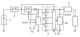
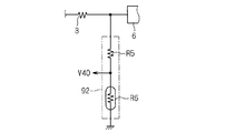
- FIG. 1 is a circuit diagram showing a capacitor unit 4, a charge / discharge control circuit for controlling charge / discharge of the capacitor unit 4, and elements connected thereto.
- the battery 1 is, for example, an in-vehicle battery and is charged by an alternator (not shown) or the like.
- the relay 2 is, for example, an ignition relay, and becomes conductive as the engine is ignited.
- One end of the current limiting resistor 3 is connected to the positive electrode of the battery 1 via the relay 2, and the other end is connected to the high potential side of the capacitor unit 4.
- the capacitor unit 4 is connected between the other end of the current limiting resistor 3 and the negative electrode of the battery 1.
- the battery 1, the relay 2, and the current limiting resistor 3 are connected in parallel to the capacitor unit 4.
- the negative electrode of the battery 1 is grounded.
- the capacitor unit 4 has capacitors 41, 42, and 43 connected in series with each other.
- the capacitor 41 is provided on the higher potential side than the capacitor 42, and the capacitor 42 is provided on the higher potential side than the capacitor 43.
- the high potential side end of the capacitor 41 is connected to the other end of the current limiting resistor 3, and the low potential side end of the capacitor 43 is connected to the negative electrode of the battery 1.
- the case where the number of capacitors included in the capacitor unit 4 is three is exemplified, but if there are a plurality of capacitors, the number can be selected as appropriate.
- the charge / discharge control circuit includes a discharge control circuit 5 and a charge control circuit 10.
- the discharge control circuit 5 individually controls the discharge of the capacitors 41, 42, and 43.
- the charging control circuit 10 collectively controls the charging of the capacitor unit 4 for all the capacitors 41, 42, and 43.
- the charge control circuit 10 includes a switch element 8 and a switch control unit 9.
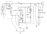
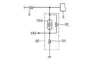
- FIG. 2 is a circuit diagram showing a part of the discharge control circuit 5 and the configuration of the charge control circuit 10.
- the converter 6 is, for example, a step-up DC / DC converter.
- the converter 6 inputs the voltage held by the capacitor unit 4, boosts it, and applies it to the load 7.
- the load 7 is, for example, a door unlocking motor.
- the switch element 8 is inserted in a charging path to the capacitor unit 4 (here, a path in which the battery 1, the relay 2, and the current limiting resistor 3 are connected in series).
- the switch element 8 includes, for example, a PMOS transistor 81 (see FIG. 2).
- the switch control unit 9 controls opening and closing of the switch element 8.
- switch control unit 9 includes a first voltage dividing circuit 92 and a comparison result output circuit 91.
- the first voltage dividing circuit 92 has a function of dividing the voltage V4 held by the capacitor unit 4 and outputting a potential V40, and includes a pair of resistance elements Rth and R1. The temperature dependence of the resistance values of the pair of resistance elements Rth and R1 is different from each other.
- the comparison result output circuit 91 controls opening and closing of the switch element 8 based on the result of comparing the potential V40 and the predetermined potential Vref1.
- the comparison result output circuit 91 includes a comparator 9a and an NMOS transistor 9b, for example.
- the output of the comparator 9a becomes a low potential and the NMOS transistor 9b is turned off.
- the PMOS transistor 81 is turned off with its gate potential rising. Therefore, the switch element 8 becomes non-conductive.
- the output of the comparator 9a becomes a high potential
- the NMOS transistor 9b is turned on
- the gate potential of the PMOS transistor 81 is lowered.
- the PMOS transistor 81 is turned on and the switch element 8 becomes conductive.
- the potential V40 is obtained by dividing the voltage V4 held by the capacitor unit 4 by the first voltage dividing circuit 92, and this is supplied to the comparison result output circuit 91. Thereby, all the capacitors 41, 42 and 43 are charged in consideration of the temperature, and the voltage held by the capacitor unit 4 is controlled according to the environmental temperature. Moreover, all of the capacitors 41, 42 and 43 connected in series are used.
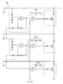
- FIG. 3 is a circuit diagram showing a configuration of the discharge controller 50.
- the discharge control unit 50 includes a plurality of discharge units 510, 520, and 530 connected in series, and input terminals 51, 52, and 53.
- Discharge units 510, 520, and 530 are provided corresponding to capacitors 41, 42, and 43, respectively.
- the discharge units 510, 520, and 530 are provided in the same number as the capacitors 41, 42, and 43 included in the capacitor unit 4.
- the input terminal 51 is on the high potential side of the capacitor 41
- the input terminal 52 is on the low potential side of the capacitor 41 and the high potential side of the capacitor 42
- the input terminal 53 is on the low potential side of the capacitor 42 and the high potential side of the capacitor 43.
- the discharge control unit 50 may include more discharge units than the number of capacitors included in the capacitor unit 4.
- the discharge part that does not correspond to the capacitor in other words, an excess has no direct relation to the operation of the present embodiment.
- the discharge unit 510 includes a differential amplifier circuit 51a, a comparator 51b, and a switch element 51c.
- the differential amplifier circuit 51a can be configured using, for example, an operational amplifier and a resistance element.
- the differential amplifier circuit 51a outputs the voltage between the input terminals 51 and 52 (that is, the voltage held by the capacitor 41) with the low potential side (here, ground) of the capacitor unit 4 as a reference.
- the comparator 51b compares the output of the differential amplifier circuit 51a with the threshold value Vref2, and controls opening and closing of the switch element 51c based on the comparison result.
- the switch element 51 c is connected between the input terminals 51 and 52.
- the switch element 51c when the output of the differential amplifier circuit 51a exceeds the threshold value Vref2, the switch element 51c is turned on, and the capacitor 41 is discharged. If the output of the differential amplifier circuit 51a is equal to or lower than the threshold value Vref2, the switch element 51c is turned off, thereby suppressing the discharge of the capacitor 41.
- the input resistance of the operational amplifier constituting the differential amplifier circuit 51a is very large, the discharge amount of the capacitor 41 when the switch element 51c is non-conductive is small.
- the discharge unit 520 includes a differential amplifier circuit 52a, a comparator 52b, and a switch element 52c.
- the differential amplifier circuit 52 a outputs the voltage between the input terminals 52 and 53 (that is, the voltage held by the capacitor 42) with the low potential side of the capacitor unit 4 as a reference.
- the differential amplifier circuit 52a can be configured in the same manner as the differential amplifier circuit 51a.
- the comparator 52b compares the output of the differential amplifier circuit 52a with the threshold value Vref2, and controls the opening and closing of the switch element 52c based on the comparison result.
- the switch element 52 c is connected between the input terminals 52 and 53. Therefore, the capacitor 42 is discharged if the output of the differential amplifier circuit 52a exceeds the threshold value Vref2, and the discharge of the capacitor 42 is suppressed if the output of the differential amplifier circuit 52a is equal to or less than the threshold value Vref2.
- the discharge unit 530 includes the comparator 53b and the switch element 53c, but does not require a differential amplifier circuit. This is because the potential of the capacitor 43 is based on the low potential side of the capacitor unit 4.
- the potential of the input terminal 53 is compared with the threshold value Vref2 by the comparator 53b, and the opening / closing of the switch element 53c is controlled based on the comparison result.
- the capacitor 43 Since the switch element 53c is connected between the input terminal 53 and the low potential side of the capacitor unit 4, the capacitor 43 is discharged when the potential at the input terminal 53 exceeds the threshold value Vref2, and the capacitor 43 when the potential is equal to or lower than the threshold value Vref2. Is suppressed.
- the discharge units 510, 520, and 530 compare the voltage held by each of the capacitors 41, 42, and 43 with the same threshold value Vref2, and each of the capacitors 41, 42, and 43 The discharge of each is controlled individually. Therefore, the capacitor unit 4 is configured to equalize the charging voltages of the capacitors 41, 42, 43 connected in series, and suppress deterioration due to uneven charging voltage.
- the discharge control circuit 5 further includes a second voltage dividing circuit 54.
- the second voltage dividing circuit 54 includes, for example, a pair of resistance elements R3 and R4 connected in series between the high potential side and the low potential side of the capacitor unit 4 with reference to FIG. Is done.
- Resistance elements R3 and R4 are arranged on the high potential side and the low potential side of capacitor unit 4, respectively.
- the resistance value of the resistance element R3 is set to (N ⁇ 1) times the resistance value of the resistance element R4.
- the threshold value Vref2 also continues to increase, so that the voltages V41, V42, and V43 also continue to increase.
- the voltage V41 which is larger than the voltage 2.1V at time 60s, decreases toward the voltage 2.1V (discharge of the capacitor 41 by the switch element 51c).
- the voltage V43 which was smaller than the voltage 2.1V at time 60s, rises toward the voltage 2.1V. This is because the accumulated charge charges the capacitor 43 when the capacitor 41 is discharged.
- the predetermined potential Vref1 is a positive value based on the low potential side (here, ground) of the capacitor unit 4 in the above configuration will be described more specifically.
- the resistance value of the resistance element R1 connected to the low potential side is higher than the first temperature coefficient of the resistance value of the resistance element Rth connected to the high potential side of the capacitor unit 4.
- the second temperature coefficient is higher.
- the resistance element R1 is a normal resistance element and has a positive temperature coefficient.
- the resistance element Rth employs a thermistor of a type having a negative temperature coefficient.
- the resistance value Rtth at the ambient temperature Tth is expressed by the following equation using the resistance value R0 at the reference temperature T0 and the thermistor coefficient B. .
- the voltage V4 held by the capacitor unit 4 is converted to a higher potential V40 as the environmental temperature increases. Therefore, as the environmental temperature is higher, the switch element 8 becomes non-conductive at a lower voltage of the capacitor unit, so that the voltage held by the capacitors 41, 42, and 43 can be set lower. As described above, the higher the environmental temperature is, the lower the voltage held by the capacitor is as described above.
- FIG. 5 is a graph schematically showing the relationship of the voltage V4 obtained by the above operation to the environmental temperature. The graph shows that the capacitor voltage decreases as the environmental temperature increases.
- the switch element 8 can be made non-conductive when the second temperature coefficient is higher than the first temperature coefficient and the potential V40 is higher than the predetermined potential Vref1.
- FIG. 6 is a circuit diagram showing a modification of the first voltage dividing circuit 92.
- the first voltage dividing circuit 92 according to the modification has a configuration in which resistance elements Rth and R1 are replaced with resistance elements R5 and R6, respectively, with respect to the first voltage dividing circuit 92 shown in FIG.
- the second temperature coefficient of the resistance value of the resistance element R6 is higher than the first temperature coefficient of the resistance value of the resistance element R5.
- the resistance element R1 is a normal resistance element and has a positive temperature coefficient.
- the resistance element R6 employs a thermistor of a type having a positive temperature coefficient.
- the voltage V4 is converted to a higher voltage as the environmental temperature is higher. Therefore, as the environmental temperature is higher, the capacitor unit 4 is less likely to be charged, and the voltage V4 and thus V41, V42, and V43 can be suppressed.
- the second temperature coefficient is lower than the first temperature coefficient
- the other configuration of the comparison result output circuit 91 may be changed as appropriate, for example, by replacing the inverting input terminal and the non-inverting input terminal of the comparator 9a.
- FIG. 7 is a circuit diagram showing a further modification of the first voltage dividing circuit 92.
- the first voltage dividing circuit 92 according to the modification is characterized in that a resistive element R2 is connected in parallel to the resistive element Rth with respect to the first voltage dividing circuit 92 shown in FIG.
- the third temperature coefficient of the resistance value of the resistance element R2 is higher than the first temperature coefficient of the resistance value of the resistance element Rth.
- each said structure can be combined suitably as long as there is no contradiction mutually.
- Capacitor unit 41, 42, 43 Capacitor 5 Discharge control circuit 510, 520, 530 Discharge unit 54, 92 Voltage divider circuit 8 Switch element 9 Switch control unit R1, R2, Rth Resistance element
Landscapes
- Engineering & Computer Science (AREA)
- Power Engineering (AREA)
- Charge And Discharge Circuits For Batteries Or The Like (AREA)
- Secondary Cells (AREA)
Abstract
直列に接続された複数のキャパシタを全て有効に活用しつつ、環境温度に応じてキャパシタユニットが保持する電圧を制御する。キャパシタユニットへの充電経路に介挿されたスイッチ素子と、スイッチ素子の開閉を制御するスイッチ制御部とが設けられる。スイッチ制御部は、キャパシタユニットが保持する電圧を分圧して出力する一対の抵抗素子を有する第1分圧回路と、第1分圧回路から出力される電位と所定電位とを比較した結果に基づいてスイッチ素子の開閉を制御する比較結果出力回路とを含む。抵抗素子のそれぞれの抵抗値の温度依存性は相互に異なる。
Description
この発明は、放電制御回路に関し、例えばキャパシタを用いたサブバッテリ回路を充放電する技術に適用される。
近年、燃費を上げるためにハイブリッドカーや電気自動車の開発が進んでいる。ガソリン車においてもアイドリングストップ等を実施し、燃費向上が望まれている。
しかしアイドリングストップ等で一旦エンジンが停止すると、オルタネータによるバッテリの充電が行われなくなる。このため、再度エンジンを点火する際には、バッテリ電圧が急激に低下する、「クランキング」と呼ばれる現象が発生する。
クランキングが発生してバッテリ電圧が急激に低下すると、自動車のボディECU(電子制御ユニット)が誤って低電圧リセットを掛けてしまう恐れがある。
このような事態を回避するため、バッテリとは別に、大容量キャパシタなどのサブバッテリを備え、クランキングに対応する技術が周知である。
このサブバッテリは例えば、クランキング対策の他、車両が衝突した際にバッテリが喪失したときの、ドアロック解除用の補助電源としても採用される。
サブバッテリで使用されるキャパシタは経年劣化により、静電容量の低下、内部抵抗の上昇が発生する。この経年劣化の進行は一般的にアレニウス則として知られており、環境温度については10℃2倍則に従う。
また、キャパシタの劣化の進行には充電電圧も影響を与える。環境温度が一定であれば、充電電圧が低いほど、劣化しにくい。
このようなキャパシタを用いたサブバッテリ回路で、キャパシタの劣化を抑制し、環境温度の変化に対応して必要なエネルギーを供給する技術が、下掲の特許文献1に例示されている。
具体的には、下掲の特許文献1には、
(i)主電源たるバッテリから補助電源たるキャパシタユニットへの充電:
(ii)キャパシタユニットを構成する複数のキャパシタの一部の充電停止:
(iii)上記(ii)の充電停止、及び充電の再開の判断は、キャパシタユニット近傍の温度に依拠する:
が記載されている。
(i)主電源たるバッテリから補助電源たるキャパシタユニットへの充電:
(ii)キャパシタユニットを構成する複数のキャパシタの一部の充電停止:
(iii)上記(ii)の充電停止、及び充電の再開の判断は、キャパシタユニット近傍の温度に依拠する:
が記載されている。
そして上記(i)~(iii)の制御により、環境温度が高いときにはキャパシタユニットへの充電電圧を低くし、以てキャパシタの劣化を抑えつつキャパシタユニットが給電するエネルギーが確保される。
また、特許文献2には、組電池を構成する複数の電池毎にバイパス回路を設ける技術が紹介されている。そしてある電池が所定の充電電位を越えた場合に、当該電池に対応するバイパス回路を導通させ、電池同士の充電電圧の不均等が低減されている。
しかし、特許文献1に紹介された技術では、(ii)で示されるように、一部のキャパシタが充電されるか否かという段階的な制御が行われる。これは(iii)で示される温度に依拠した制御が容易ではない。換言すると充電の停止/再開を設定する温度閾値の設定が難しい。しかも、環境温度が高いときに給電に寄与しないキャパシタが存在することは、キャパシタユニットに設けられたキャパシタを有効に使用できていないことになり、コスト的に不利となる。
また、特許文献2に紹介された技術では、充電する電圧は一意にしか決定できず、温度による充電電圧の変化を行うことは示唆されていない。
そこで、本発明は、直列に接続された複数のキャパシタを全て有効に活用しつつ、環境温度に応じてキャパシタユニットが保持する電圧を制御する技術を提供することを目的とする。
第1の態様は、互いに直列に接続された複数のキャパシタを有するキャパシタユニットを充放電する充放電制御回路である。そして前記キャパシタの放電を個別に制御する放電制御回路と、前記キャパシタユニットの充電を前記キャパシタの全てを一括して制御する充電制御回路とを備える。前記充電制御回路は、前記キャパシタユニットへの充電経路に介挿されたスイッチ素子と、前記スイッチ素子の開閉を制御するスイッチ制御部とを有する。前記スイッチ制御部は、前記キャパシタユニットが保持する電圧を分圧して出力する一対の抵抗素子を有する第1分圧回路と、前記第1分圧回路から出力される電位と所定電位とを比較した結果に基づいて前記スイッチ素子の開閉を制御する比較結果出力回路とを含む。前記一対の抵抗素子のそれぞれの抵抗値の温度依存性は相互に異なる。
第2の態様は第1の態様に係る充放電制御回路であって、前記放電制御回路は、前記複数のキャパシタの各々が保持する電圧を、同一の閾値と比較して、前記複数のキャパシタの各々の放電を個別に制御する、複数の放電部と、前記キャパシタユニットが保持する前記電圧を、前記キャパシタユニットにおいて直列に接続される前記キャパシタの個数で除した値に分圧して前記閾値として出力する第2分圧回路とを有する。
第3の態様は第1の態様又は第2の態様に係る充放電制御回路であって、前記所定電位は正値であり、前記一対の抵抗素子のうち、前記キャパシタユニットの高電位側に接続される第1の抵抗素子の抵抗値は第1の温度係数を有し、前記一対の抵抗素子のうち、前記キャパシタユニットの低電位側に接続される第2の抵抗素子の抵抗値は前記第1の温度係数よりも高い第2の温度係数を有し、比較結果出力回路は、前記第1分圧回路から出力された前記電位が前記所定電位を越えることによって前記スイッチ素子を非導通とする。
第4の態様は第3の態様に係る充放電制御回路であって、前記第1の温度係数は負の温度係数であり、前記第2の温度係数は正の温度係数である。
第5の態様は第3の態様又は第4の態様に係る充放電制御回路であって、前記第1分圧回路は、前記第1の抵抗素子に対して並列に接続され、前記第1の温度係数よりも高い第3の温度係数を有する第3の抵抗素子を更に有する。
第1の態様によると、キャパシタユニットの電圧が温度を考慮した電圧に変換されて比較結果出力回路に与えられる。これにより、キャパシタの全てについて、温度を考慮した充電が行われ、以てキャパシタユニットが保持する電圧は環境温度に応じて制御される。しかも直列に接続されたキャパシタの全てが利用される。
第2の態様によると、キャパシタユニットを構成して直列に接続される複数のキャパシタ同士の充電電圧を均等化し、充電電圧の不均一による劣化を抑制する。
第3の態様によると、キャパシタユニットの電圧は環境温度が高いほど高い電圧へ分圧される。よって、環境温度が高いほど、低いキャパシタユニットの電圧でスイッチ素子が非導通となり、以てキャパシタの各々が保持する電圧を低く設定できる。
第4の態様によると、第3の態様における第1の抵抗素子と第2の抵抗素子を容易に選定できる。
第5の態様によると、キャパシタの電圧から接続点の電位への変換の、微調整が容易である。
以下、実施形態に係る充放電制御回路について説明する。図1は、キャパシタユニット4と、キャパシタユニット4の充放電を制御する充放電制御回路、及びこれらと接続される要素について示す回路図である。
バッテリ1は、例えば車載用のバッテリであり、不図示のオルタネータ等によって充電される。リレー2は例えばイグニッションリレーであり、エンジン点火に伴って導通する。電流制限抵抗3の一端はリレー2を介してバッテリ1の正極に接続されており、他端はキャパシタユニット4の高電位側に接続される。
キャパシタユニット4は電流制限抵抗3の他端と、バッテリ1の負極との間に接続されている。換言すれば、バッテリ1、リレー2、電流制限抵抗3はキャパシタユニット4に対して並列に接続されている。なお、図1ではバッテリ1の負極は接地されている。
キャパシタユニット4は互いに直列に接続されたキャパシタ41,42,43を有している。キャパシタ41はキャパシタ42よりも、キャパシタ42はキャパシタ43よりも、それぞれ高電位側に設けられる。キャパシタ41の高電位側端は電流制限抵抗3の他端に接続され、キャパシタ43の低電位側端はバッテリ1の負極に接続される。
ここではキャパシタユニット4が有するキャパシタの個数として3個の場合が例示されたが、複数であればその個数は適宜選定できる。
充放電制御回路は放電制御回路5と、充電制御回路10とを備える。放電制御回路5は、キャパシタ41,42,43の放電を個別に制御する。充電制御回路10は、キャパシタユニット4の充電をキャパシタ41,42,43の全てを一括して制御する。充電制御回路10は、スイッチ素子8とスイッチ制御部9とを有している。図2に、放電制御回路5の一部と、充電制御回路10の構成を回路図で示す。
コンバータ6は、例えば昇圧DC/DCコンバータである。例えばコンバータ6は、キャパシタユニット4が保持する電圧を入力し、これを昇圧して負荷7に与える。負荷7は例えばドアロック解除用のモータである。
スイッチ素子8は、キャパシタユニット4への充電経路(ここではバッテリ1、リレー2、電流制限抵抗3が直列に接続される経路)に介挿される。スイッチ素子8は、例えばPMOSトランジスタ81を含んで構成される(図2参照)。
スイッチ制御部9は、スイッチ素子8の開閉を制御する。図2を参照して、スイッチ制御部9は、第1分圧回路92と、比較結果出力回路91とを含む。第1分圧回路92は、キャパシタユニット4が保持する電圧V4を分圧して電位V40を出力する機能を有し、一対の抵抗素子Rth,R1を有する。一対の抵抗素子Rth,R1のそれぞれの抵抗値の温度依存性は相互に異なる。
比較結果出力回路91は、電位V40と所定電位Vref1とを比較した結果に基づいて、スイッチ素子8の開閉を制御する。比較結果出力回路91は例えばコンパレータ9a、NMOSトランジスタ9bを含んで構成される。
以下、リレー2がオンしている状況において説明する。スイッチ素子8がオンしていると、バッテリ1によってキャパシタユニット4へと充電電流が供給される。スイッチ素子8がオフすると、充電電流の供給は遮断される。
電位V40が所定電位Vref1を越えると、コンパレータ9aの出力は低電位となり、NMOSトランジスタ9bをオフする。NMOSトランジスタ9bがオフすると、PMOSトランジスタ81は、そのゲート電位が上昇してオフする。よってスイッチ素子8が非導通となる。
電位V40が所定電位Vref1以下であれば、コンパレータ9aの出力は高電位となり、NMOSトランジスタ9bがオンしてPMOSトランジスタ81のゲート電位を下げる。これによりPMOSトランジスタ81はオンして、スイッチ素子8が導通する。
電位V40は第1分圧回路92によってキャパシタユニット4が保持する電圧V4を分圧したものであり、これが比較結果出力回路91に与えられる。これにより、キャパシタ41,42,43の全てについて、温度を考慮した充電が行われ、以てキャパシタユニット4が保持する電圧は環境温度に応じて制御される。しかも直列に接続されたキャパシタ41,42,43の全てが利用される。
図3は放電制御部50の構成を示す回路図である。放電制御部50は、直列に接続された複数の放電部510,520,530と、入力端51,52,53とを備える。
放電部510,520,530は、それぞれキャパシタ41,42,43に対応して備えられる。放電制御部50において放電部510,520,530は、キャパシタユニット4が有するキャパシタ41,42,43の個数と同じ個数が設けられる。
ここでは入力端51はキャパシタ41の高電位側に、入力端52はキャパシタ41の低電位側及びキャパシタ42の高電位側に、入力端53はキャパシタ42の低電位側及びキャパシタ43の高電位側に、それぞれ接続される。
もちろん、放電制御部50は、キャパシタユニット4が有するキャパシタの個数よりも多くの放電部を備えてもよい。しかしキャパシタに対応しない(言ってみれば余剰の)放電部は本実施形態の動作とは直接の関連はない。
放電部510は差動増幅回路51aとコンパレータ51bと、スイッチ素子51cとを有する。差動増幅回路51aは例えばオペアンプと抵抗素子とを用いて構成できる。差動増幅回路51aは入力端51,52間の電圧(つまりキャパシタ41が保持する電圧)を、キャパシタユニット4の低電位側(ここでは接地)を基準として出力する。
コンパレータ51bは差動増幅回路51aの出力と閾値Vref2とを比較し、その比較結果に基づいてスイッチ素子51cの開閉を制御する。スイッチ素子51cは入力端51,52の間に接続される。
具体的には差動増幅回路51aの出力が閾値Vref2を越えればスイッチ素子51cを導通させ、以てキャパシタ41を放電させる。差動増幅回路51aの出力が閾値Vref2以下であればスイッチ素子51cを非導通とし、以てキャパシタ41の放電を抑制する。通常、差動増幅回路51aを構成するオペアンプの入力抵抗は非常に大きいので、スイッチ素子51cが非導通のときのキャパシタ41の放電量は小さい。
放電部520は差動増幅回路52aとコンパレータ52bと、スイッチ素子52cとを有する。差動増幅回路52aは入力端52,53間の電圧(つまりキャパシタ42が保持する電圧)を、キャパシタユニット4の低電位側を基準として出力する。差動増幅回路52aも差動増幅回路51aと同様にして構成できる。
コンパレータ52bは差動増幅回路52aの出力と閾値Vref2とを比較し、その比較結果に基づいてスイッチ素子52cの開閉を制御する。スイッチ素子52cは入力端52,53の間に接続される。よって差動増幅回路52aの出力が閾値Vref2を越えればキャパシタ42が放電し、差動増幅回路52aの出力が閾値Vref2以下であればキャパシタ42の放電が抑制される。
放電部530も放電部510,520と同様にして、コンパレータ53bとスイッチ素子53cとを有するが、差動増幅回路は必要としない。キャパシタ43の電位はキャパシタユニット4の低電位側を基準としているからである。
入力端53の電位が、コンパレータ53bによって閾値Vref2とを比較され、その比較結果に基づいてスイッチ素子53cの開閉が制御される。
スイッチ素子53cは入力端53と、キャパシタユニット4の低電位側との間に接続されるので、入力端53の電位が閾値Vref2を越えればキャパシタ43が放電し、閾値Vref2以下であればキャパシタ43の放電が抑制される。
キャパシタユニットに設けられた(少なくとも一つの)キャパシタを、これに並列に接続されたスイッチ素子の開閉によって、充放電すること自体は公知であるので、これ以上の放電部510,520,530の動作の詳細な説明は避ける。
このように、放電制御回路5において、放電部510,520,530は、キャパシタ41,42,43の各々が保持する電圧を、同一の閾値Vref2と比較して、キャパシタ41,42,43の各々の放電を個別に制御する。よってキャパシタユニット4を構成して直列に接続されるキャパシタ41,42,43同士の充電電圧を均等化し、充電電圧の不均一による劣化を抑制する。
但し、上記の説明から理解されるように、キャパシタ41,42,43の放電の有無は、それぞれが保持する電圧と、閾値Vref2との比較結果に依存する。そしてキャパシタユニット4ではキャパシタ41,42,43が直列に接続されているのであるから、閾値Vref2はキャパシタユニット4が保持する電圧V4の1/3倍でなければならない。
そこで、放電制御回路5は更に、第2分圧回路54を有する。第2分圧回路54は、電圧V4を、キャパシタユニット4において直列に接続されるキャパシタ41,42,43の個数N個(ここではN=3)で除した値V4×(1/N)に分圧して閾値Vref2として出力する。
第2分圧回路54は具体的には例えば図2を参照して、キャパシタユニット4の高電位側と低電位側との間で直列に接続される一対の抵抗素子R3,R4を含んで構成される。抵抗素子R3,R4はそれぞれキャパシタユニット4の高電位側と低電位側とに配置される。抵抗素子R3の抵抗値は抵抗素子R4の抵抗値の(N-1)倍に設定される。これにより閾値Vref2=V4×(1/N)が、抵抗素子R3,R4同士の接続点から得られることになる。
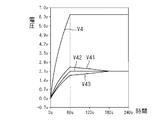
図4は、キャパシタユニット4が保持する電圧V4、キャパシタ41,42,43がそれぞれ保持する電圧V41,V42,V43の時間依存性を示すグラフである。キャパシタユニット4ではキャパシタ41,42,43が直列に接続されているのであるから、V4=V41+V42+V43の関係がある。
初期状態として、キャパシタ41,42,43が完全に放電されており、V4=V41=V42=V43=0となる場合を設定している。また、理解を容易にするために、キャパシタ41,42,43の静電容量C41,C42,C43を、C41<C42<C43に設定した。
時刻0sには、リレー2の導通を開始した時点を採用した。それ以前にはV4=0であるので、スイッチ素子8は導通し、時刻0s以降、キャパシタユニット4はバッテリ1によって充電される。
上述のようにC41<C42<C43であるので、キャパシタユニット4への充電が行われている間はV41>V42>V43となっている。
さて、キャパシタユニット4への充電により、電圧V4は上昇し続ける。電圧V4が上昇し続ける間は、閾値Vref2も上昇し続けるので、電圧V41,V42,V43も上昇し続ける。
時刻60sにおいて電圧V4がほぼ6.3Vに達すると、スイッチ制御部9の機能により、スイッチ素子8が非導通となる。この後、キャパシタ41,42,43の微少な放電により電圧V4が低下すると、再びスイッチ素子8は導通してキャパシタユニット4への充電が再開される。よってこれ以降、電圧V4は振動しつつも6.3V近傍で維持される。但し、図4ではこの振動(電圧V41,V42,V43についても同様)については無視して描いている。
このように電圧V4がほぼ6.3Vでほぼ一定値となるので、閾値Vref2は6.3/2=2.1V程度で一定値となる。このため、時刻60sにおいて電圧2.1V近傍にあった電圧V42はその値を維持し続ける。
他方、時刻60sにおいて電圧2.1Vよりも大きな値であった電圧V41は電圧2.1Vに向けて低下する(スイッチ素子51cによるキャパシタ41の放電)。
また時刻60sにおいて電圧2.1Vよりも小さな値であった電圧V43は電圧2.1Vに向けて上昇する。これはキャパシタ41が放電されることにより、その蓄積していた電荷がキャパシタ43を充電するからである。
このようにして、時刻180s付近では、電圧V41,V42,V43のいずれもがほぼ2.1Vに等しくなり、その後もこれらの電圧が維持される。
上述の構成において所定電位Vref1がキャパシタユニット4の低電位側(ここでは接地)を基準とした正値とする場合について、より具体的に説明する。抵抗素子Rth,R1のうち、キャパシタユニット4の高電位側に接続される抵抗素子Rthの抵抗値が有する第1の温度係数よりも、低電位側に接続される抵抗素子R1の抵抗値が有する第2の温度係数の方が高い。
例えば抵抗素子R1は通常の抵抗素子であって、正の温度係数を有する。例えば抵抗素子Rthは負の温度係数を有するタイプのサーミスタを採用する。
負の温度係数を有するタイプのサーミスタでは、その環境温度Tthにおける抵抗値Rtthは、基準温度T0における抵抗値R0と、サーミスタ係数Bとを用いて、下式のように示されることが公知である。
Rtth=R0・exp[B・(1/Tth-1/T0)]
但し、記号exp[]は、括弧内の値の指数関数を示す。
よってキャパシタユニット4が保持する電圧V4は環境温度が高いほど高い電位V40へ変換される。よって、環境温度が高いほど、低いキャパシタユニットの電圧でスイッチ素子8が非導通となり、以てキャパシタ41,42,43が保持する電圧を低く設定できる。このように環境温度が高いほど、キャパシタが保持する電圧を低くすることが望ましいのは、上述の通りである。
図5は上述の動作によって得られる電圧V4の、環境温度に対する関係を模式的に示すグラフである。当該グラフにおいて、環境温度が上昇するほど、キャパシタ電圧は低下することが示されている。
もちろん、第1の温度係数と、第2の温度係数とはその極性が異なることを前提とするものではない。第1の温度係数よりも第2の温度係数の方が高く、電位V40が所定電位Vref1よりも高いときにスイッチ素子8を非導通させることができればよい。
図6は第1分圧回路92の変形を示す回路図である。当該変形にかかる第1分圧回路92は、図2に示された第1分圧回路92に対し、抵抗素子Rth,R1をそれぞれ抵抗素子R5,R6に置換した構成を有している。
抵抗素子Rth,R1と類似して、抵抗素子R5の抵抗値が有する第1の温度係数よりも、抵抗素子R6の抵抗値が有する第2の温度係数の方が高い。但し抵抗素子R1は通常の抵抗素子であって、正の温度係数を有する。例えば抵抗素子R6は正の温度係数を有するタイプのサーミスタを採用する。
このような場合でも、電圧V4は環境温度が高いほど高い電圧に変換される。よって環境温度が高いほどキャパシタユニット4は充電されにくくなり、電圧V4を、ひいてはV41,V42,V43を抑制できる。
あるいは第1の温度係数よりも第2の温度係数の方が低い構成を採用することもできる。この場合、比較結果出力回路91として他の構成を、たとえばコンパレータ9aの反転入力端と非反転入力端とを入れ替えるなどの適宜の設計変更を行えばよい。
図7は第1分圧回路92の更なる変形を示す回路図である。当該変形にかかる第1分圧回路92は、図2に示された第1分圧回路92に対し、抵抗素子Rthに対して抵抗素子R2を並列に接続した点が特徴である。抵抗素子R2の抵抗値が有する第3の温度係数は、抵抗素子Rthの抵抗値が有する第1の温度係数よりも高い。
このようにすれば、環境温度に応じた電圧V4から電位V40への変換の、微調整が容易となる。
なお、上記各構成は、相互に矛盾しない限り適宜組合わせることができる。
以上のようにこの発明は詳細に説明されたが、上記した説明は、すべての局面において、例示であって、この発明がそれに限定されるものではない。例示されていない無数の変形例が、この発明の範囲から外れることなく想定され得るものと解される。
4 キャパシタユニット
41,42,43 キャパシタ
5 放電制御回路
510,520,530 放電部
54,92 分圧回路
8 スイッチ素子
9 スイッチ制御部
R1,R2,Rth 抵抗素子
41,42,43 キャパシタ
5 放電制御回路
510,520,530 放電部
54,92 分圧回路
8 スイッチ素子
9 スイッチ制御部
R1,R2,Rth 抵抗素子
Claims (5)
- 互いに直列に接続された複数のキャパシタを有するキャパシタユニットを充放電する充放電制御回路であって、
前記キャパシタの放電を個別に制御する放電制御回路と、
前記キャパシタユニットの充電を前記キャパシタの全てを一括して制御する充電制御回路と
を備え、
前記充電制御回路は、
前記キャパシタユニットへの充電経路に介挿されたスイッチ素子と、
前記スイッチ素子の開閉を制御するスイッチ制御部と
を有し、
前記スイッチ制御部は、
前記キャパシタユニットが保持する電圧を分圧して出力する一対の抵抗素子を有する第1分圧回路と、
前記第1分圧回路から出力される電位と所定電位とを比較した結果に基づいて前記スイッチ素子の開閉を制御する比較結果出力回路と
を含み、
前記一対の抵抗素子のそれぞれの抵抗値の温度依存性は相互に異なる、充放電制御回路。 - 請求項1に記載の充放電制御回路であって、
前記放電制御回路は、
前記複数のキャパシタの各々が保持する電圧を、同一の閾値と比較して、前記複数のキャパシタの各々の放電を個別に制御する、複数の放電部と、
前記キャパシタユニットが保持する前記電圧を、前記キャパシタユニットにおいて直列に接続される前記キャパシタの個数で除した値に分圧して前記閾値として出力する第2分圧回路と
を有する、充放電制御回路。 - 請求項1又は請求項2に記載の充放電制御回路であって、
前記所定電位は正値であり、
前記一対の抵抗素子のうち、前記キャパシタユニットの高電位側に接続される第1の抵抗素子の抵抗値は第1の温度係数を有し、
前記一対の抵抗素子のうち、前記キャパシタユニットの低電位側に接続される第2の抵抗素子の抵抗値は前記第1の温度係数よりも高い第2の温度係数を有し、
比較結果出力回路は、前記第1分圧回路から出力された前記電位が前記所定電位を越えることによって前記スイッチ素子を非導通とする、充放電制御回路。 - 請求項3に記載の充放電制御回路であって、
前記第1の温度係数は負の温度係数であり、前記第2の温度係数は正の温度係数である、充放電制御回路。 - 請求項3又は請求項4に記載の充放電制御回路であって、
前記第1分圧回路は、
前記第1の抵抗素子に対して並列に接続され、前記第1の温度係数よりも高い第3の温度係数を有する第3の抵抗素子
を更に有する、充放電制御回路。
Priority Applications (2)
| Application Number | Priority Date | Filing Date | Title |
|---|---|---|---|
| US15/514,336 US20170288424A1 (en) | 2014-09-29 | 2015-09-15 | Charge-discharge control circuit |
| CN201580051336.3A CN106716768A (zh) | 2014-09-29 | 2015-09-15 | 充放电控制电路 |
Applications Claiming Priority (2)
| Application Number | Priority Date | Filing Date | Title |
|---|---|---|---|
| JP2014-198293 | 2014-09-29 | ||
| JP2014198293A JP2016073044A (ja) | 2014-09-29 | 2014-09-29 | 充放電制御回路 |
Publications (1)
| Publication Number | Publication Date |
|---|---|
| WO2016052163A1 true WO2016052163A1 (ja) | 2016-04-07 |
Family
ID=55630205
Family Applications (1)
| Application Number | Title | Priority Date | Filing Date |
|---|---|---|---|
| PCT/JP2015/076077 WO2016052163A1 (ja) | 2014-09-29 | 2015-09-15 | 充放電制御回路 |
Country Status (4)
| Country | Link |
|---|---|
| US (1) | US20170288424A1 (ja) |
| JP (1) | JP2016073044A (ja) |
| CN (1) | CN106716768A (ja) |
| WO (1) | WO2016052163A1 (ja) |
Cited By (1)
| Publication number | Priority date | Publication date | Assignee | Title |
|---|---|---|---|---|
| US20230123946A1 (en) * | 2021-10-14 | 2023-04-20 | Amogy Inc. | Power management for hybrid power system |
Families Citing this family (3)
| Publication number | Priority date | Publication date | Assignee | Title |
|---|---|---|---|---|
| US10254177B2 (en) * | 2016-09-14 | 2019-04-09 | Nxp B.V. | Temperature-to-digital converter |
| GB2561178A (en) * | 2017-04-03 | 2018-10-10 | Ford Global Tech Llc | Improvements in or relating to oil sensors |
| CN110994956B (zh) * | 2019-12-17 | 2021-04-30 | 海信(山东)空调有限公司 | 一种电解电容的充电电路及其控制方法、控制装置 |
Citations (5)
| Publication number | Priority date | Publication date | Assignee | Title |
|---|---|---|---|---|
| JPH05292684A (ja) * | 1992-04-03 | 1993-11-05 | Jeol Ltd | 動力用蓄電電源装置 |
| JP2009005558A (ja) * | 2007-06-25 | 2009-01-08 | Mitsumi Electric Co Ltd | 電池パック |
| WO2009078136A1 (ja) * | 2007-12-18 | 2009-06-25 | Panasonic Corporation | 電圧均等化回路 |
| EP2390952A2 (en) * | 2010-05-28 | 2011-11-30 | Sony Corporation | Solar power-generating equipment |
| JP2013126313A (ja) * | 2011-12-15 | 2013-06-24 | Panasonic Corp | キャパシタ装置 |
Family Cites Families (5)
| Publication number | Priority date | Publication date | Assignee | Title |
|---|---|---|---|---|
| JPH11187584A (ja) * | 1997-12-18 | 1999-07-09 | Tamura Electric Works Ltd | 携帯端末装置 |
| JP2000152516A (ja) * | 1998-11-13 | 2000-05-30 | Nec Saitama Ltd | 電池パック温度保護回路 |
| JP4440717B2 (ja) * | 2004-06-30 | 2010-03-24 | 新電元工業株式会社 | 直流電圧供給装置 |
| JP4970854B2 (ja) * | 2006-03-08 | 2012-07-11 | 株式会社リコー | 画像形成装置及び制御方法 |
| DE102008056962A1 (de) * | 2008-11-03 | 2010-05-06 | Stribel Production Gmbh | System zur Überwachung von Kondensatorzellen |
-
2014
- 2014-09-29 JP JP2014198293A patent/JP2016073044A/ja active Pending
-
2015
- 2015-09-15 CN CN201580051336.3A patent/CN106716768A/zh active Pending
- 2015-09-15 WO PCT/JP2015/076077 patent/WO2016052163A1/ja active Application Filing
- 2015-09-15 US US15/514,336 patent/US20170288424A1/en not_active Abandoned
Patent Citations (6)
| Publication number | Priority date | Publication date | Assignee | Title |
|---|---|---|---|---|
| JPH05292684A (ja) * | 1992-04-03 | 1993-11-05 | Jeol Ltd | 動力用蓄電電源装置 |
| JP2009005558A (ja) * | 2007-06-25 | 2009-01-08 | Mitsumi Electric Co Ltd | 電池パック |
| WO2009078136A1 (ja) * | 2007-12-18 | 2009-06-25 | Panasonic Corporation | 電圧均等化回路 |
| EP2390952A2 (en) * | 2010-05-28 | 2011-11-30 | Sony Corporation | Solar power-generating equipment |
| JP2012009819A (ja) * | 2010-05-28 | 2012-01-12 | Sony Corp | 太陽光発電装置 |
| JP2013126313A (ja) * | 2011-12-15 | 2013-06-24 | Panasonic Corp | キャパシタ装置 |
Cited By (2)
| Publication number | Priority date | Publication date | Assignee | Title |
|---|---|---|---|---|
| US20230123946A1 (en) * | 2021-10-14 | 2023-04-20 | Amogy Inc. | Power management for hybrid power system |
| US11923711B2 (en) * | 2021-10-14 | 2024-03-05 | Amogy Inc. | Power management for hybrid power system |
Also Published As
| Publication number | Publication date |
|---|---|
| CN106716768A (zh) | 2017-05-24 |
| JP2016073044A (ja) | 2016-05-09 |
| US20170288424A1 (en) | 2017-10-05 |
Similar Documents
| Publication | Publication Date | Title |
|---|---|---|
| WO2016052163A1 (ja) | 充放電制御回路 | |
| JP5942083B2 (ja) | キャパシタ装置 | |
| US20170113637A1 (en) | Device for connecting a base vehicle electrical system to a, in particular, safety-relevant subsystem | |
| JP6406328B2 (ja) | 電源装置及び電池ユニット | |
| US9263932B2 (en) | DC-DC converter | |
| JP2015532577A (ja) | 電圧変換のための装置並びに該装置を備えた車載電気システム | |
| JP6587794B2 (ja) | 放電制御回路及びバッテリユニット | |
| JP6112004B2 (ja) | 補助電源装置 | |
| WO2018008567A1 (ja) | 電源制御装置、及び電源システム | |
| WO2017159035A1 (ja) | 放電回路および蓄電装置 | |
| WO2022210441A1 (ja) | 予備電源装置及び予備電源装置の制御方法 | |
| US20230027762A1 (en) | Low voltage dc-dc converter of environmentally friendly vehicle, and method for outputting constant voltage using the same | |
| JP6520665B2 (ja) | 電圧測定装置、電圧測定システム | |
| JP2016073048A (ja) | 放電制御回路及びバッテリユニット | |
| JP6587432B2 (ja) | オルタネータの発電制御装置 | |
| JP2015171254A (ja) | 補助蓄電器充電制御装置 | |
| US10821840B2 (en) | Power supply arrangement with an interface for operation of a multi-voltage system | |
| JP6102721B2 (ja) | 蓄電装置及びバッテリ装置 | |
| KR101499517B1 (ko) | 전원 제어회로 및 전원제어방법 | |
| WO2017065161A1 (ja) | 電源装置及び電池ユニット | |
| WO2021187183A1 (ja) | 比較回路 | |
| KR101243007B1 (ko) | 비엠에스용 배터리 균등 제어장치 | |
| US20180265022A1 (en) | In-vehicle power supply device | |
| JP6024648B2 (ja) | 補助電源装置 | |
| JP6217167B2 (ja) | 自動車用二電源装置 |
Legal Events
| Date | Code | Title | Description |
|---|---|---|---|
| 121 | Ep: the epo has been informed by wipo that ep was designated in this application |
Ref document number: 15847789 Country of ref document: EP Kind code of ref document: A1 |
|
| WWE | Wipo information: entry into national phase |
Ref document number: 15514336 Country of ref document: US |
|
| NENP | Non-entry into the national phase |
Ref country code: DE |
|
| 122 | Ep: pct application non-entry in european phase |
Ref document number: 15847789 Country of ref document: EP Kind code of ref document: A1 |