WO2016052097A1 - スイッチ素子および記憶装置 - Google Patents
スイッチ素子および記憶装置 Download PDFInfo
- Publication number
- WO2016052097A1 WO2016052097A1 PCT/JP2015/075464 JP2015075464W WO2016052097A1 WO 2016052097 A1 WO2016052097 A1 WO 2016052097A1 JP 2015075464 W JP2015075464 W JP 2015075464W WO 2016052097 A1 WO2016052097 A1 WO 2016052097A1
- Authority
- WO
- WIPO (PCT)
- Prior art keywords
- layer
- switch
- electrode
- switch element
- resistance
- Prior art date
- Legal status (The legal status is an assumption and is not a legal conclusion. Google has not performed a legal analysis and makes no representation as to the accuracy of the status listed.)
- Ceased
Links
Images
















Classifications
-
- G—PHYSICS
- G11—INFORMATION STORAGE
- G11C—STATIC STORES
- G11C13/00—Digital stores characterised by the use of storage elements not covered by groups G11C11/00, G11C23/00, or G11C25/00
- G11C13/0002—Digital stores characterised by the use of storage elements not covered by groups G11C11/00, G11C23/00, or G11C25/00 using resistive RAM [RRAM] elements
- G11C13/0004—Digital stores characterised by the use of storage elements not covered by groups G11C11/00, G11C23/00, or G11C25/00 using resistive RAM [RRAM] elements comprising amorphous/crystalline phase transition cells
-
- G—PHYSICS
- G11—INFORMATION STORAGE
- G11C—STATIC STORES
- G11C11/00—Digital stores characterised by the use of particular electric or magnetic storage elements; Storage elements therefor
- G11C11/02—Digital stores characterised by the use of particular electric or magnetic storage elements; Storage elements therefor using magnetic elements
- G11C11/16—Digital stores characterised by the use of particular electric or magnetic storage elements; Storage elements therefor using magnetic elements using elements in which the storage effect is based on magnetic spin effect
- G11C11/165—Auxiliary circuits
- G11C11/1659—Cell access
-
- G—PHYSICS
- G11—INFORMATION STORAGE
- G11C—STATIC STORES
- G11C13/00—Digital stores characterised by the use of storage elements not covered by groups G11C11/00, G11C23/00, or G11C25/00
- G11C13/0002—Digital stores characterised by the use of storage elements not covered by groups G11C11/00, G11C23/00, or G11C25/00 using resistive RAM [RRAM] elements
- G11C13/0007—Digital stores characterised by the use of storage elements not covered by groups G11C11/00, G11C23/00, or G11C25/00 using resistive RAM [RRAM] elements comprising metal oxide memory material, e.g. perovskites
-
- G—PHYSICS
- G11—INFORMATION STORAGE
- G11C—STATIC STORES
- G11C13/00—Digital stores characterised by the use of storage elements not covered by groups G11C11/00, G11C23/00, or G11C25/00
- G11C13/0002—Digital stores characterised by the use of storage elements not covered by groups G11C11/00, G11C23/00, or G11C25/00 using resistive RAM [RRAM] elements
- G11C13/0021—Auxiliary circuits
- G11C13/003—Cell access
-
- G—PHYSICS
- G11—INFORMATION STORAGE
- G11C—STATIC STORES
- G11C13/00—Digital stores characterised by the use of storage elements not covered by groups G11C11/00, G11C23/00, or G11C25/00
- G11C13/0002—Digital stores characterised by the use of storage elements not covered by groups G11C11/00, G11C23/00, or G11C25/00 using resistive RAM [RRAM] elements
- G11C13/0021—Auxiliary circuits
- G11C13/0069—Writing or programming circuits or methods
-
- H—ELECTRICITY
- H10—SEMICONDUCTOR DEVICES; ELECTRIC SOLID-STATE DEVICES NOT OTHERWISE PROVIDED FOR
- H10B—ELECTRONIC MEMORY DEVICES
- H10B61/00—Magnetic memory devices, e.g. magnetoresistive RAM [MRAM] devices
- H10B61/10—Magnetic memory devices, e.g. magnetoresistive RAM [MRAM] devices comprising components having two electrodes, e.g. diodes or MIM elements
-
- H—ELECTRICITY
- H10—SEMICONDUCTOR DEVICES; ELECTRIC SOLID-STATE DEVICES NOT OTHERWISE PROVIDED FOR
- H10B—ELECTRONIC MEMORY DEVICES
- H10B63/00—Resistance change memory devices, e.g. resistive RAM [ReRAM] devices
- H10B63/20—Resistance change memory devices, e.g. resistive RAM [ReRAM] devices comprising selection components having two electrodes, e.g. diodes
-
- H—ELECTRICITY
- H10—SEMICONDUCTOR DEVICES; ELECTRIC SOLID-STATE DEVICES NOT OTHERWISE PROVIDED FOR
- H10B—ELECTRONIC MEMORY DEVICES
- H10B63/00—Resistance change memory devices, e.g. resistive RAM [ReRAM] devices
- H10B63/80—Arrangements comprising multiple bistable or multi-stable switching components of the same type on a plane parallel to the substrate, e.g. cross-point arrays
-
- H—ELECTRICITY
- H10—SEMICONDUCTOR DEVICES; ELECTRIC SOLID-STATE DEVICES NOT OTHERWISE PROVIDED FOR
- H10B—ELECTRONIC MEMORY DEVICES
- H10B63/00—Resistance change memory devices, e.g. resistive RAM [ReRAM] devices
- H10B63/80—Arrangements comprising multiple bistable or multi-stable switching components of the same type on a plane parallel to the substrate, e.g. cross-point arrays
- H10B63/84—Arrangements comprising multiple bistable or multi-stable switching components of the same type on a plane parallel to the substrate, e.g. cross-point arrays arranged in a direction perpendicular to the substrate, e.g. 3D cell arrays
-
- H—ELECTRICITY
- H10—SEMICONDUCTOR DEVICES; ELECTRIC SOLID-STATE DEVICES NOT OTHERWISE PROVIDED FOR
- H10N—ELECTRIC SOLID-STATE DEVICES NOT OTHERWISE PROVIDED FOR
- H10N70/00—Solid-state devices having no potential barriers, and specially adapted for rectifying, amplifying, oscillating or switching
- H10N70/20—Multistable switching devices, e.g. memristors
-
- H—ELECTRICITY
- H10—SEMICONDUCTOR DEVICES; ELECTRIC SOLID-STATE DEVICES NOT OTHERWISE PROVIDED FOR
- H10N—ELECTRIC SOLID-STATE DEVICES NOT OTHERWISE PROVIDED FOR
- H10N70/00—Solid-state devices having no potential barriers, and specially adapted for rectifying, amplifying, oscillating or switching
- H10N70/20—Multistable switching devices, e.g. memristors
- H10N70/231—Multistable switching devices, e.g. memristors based on solid-state phase change, e.g. between amorphous and crystalline phases, Ovshinsky effect
-
- H—ELECTRICITY
- H10—SEMICONDUCTOR DEVICES; ELECTRIC SOLID-STATE DEVICES NOT OTHERWISE PROVIDED FOR
- H10N—ELECTRIC SOLID-STATE DEVICES NOT OTHERWISE PROVIDED FOR
- H10N70/00—Solid-state devices having no potential barriers, and specially adapted for rectifying, amplifying, oscillating or switching
- H10N70/20—Multistable switching devices, e.g. memristors
- H10N70/24—Multistable switching devices, e.g. memristors based on migration or redistribution of ionic species, e.g. anions, vacancies
-
- H—ELECTRICITY
- H10—SEMICONDUCTOR DEVICES; ELECTRIC SOLID-STATE DEVICES NOT OTHERWISE PROVIDED FOR
- H10N—ELECTRIC SOLID-STATE DEVICES NOT OTHERWISE PROVIDED FOR
- H10N70/00—Solid-state devices having no potential barriers, and specially adapted for rectifying, amplifying, oscillating or switching
- H10N70/20—Multistable switching devices, e.g. memristors
- H10N70/24—Multistable switching devices, e.g. memristors based on migration or redistribution of ionic species, e.g. anions, vacancies
- H10N70/245—Multistable switching devices, e.g. memristors based on migration or redistribution of ionic species, e.g. anions, vacancies the species being metal cations, e.g. programmable metallization cells
-
- H—ELECTRICITY
- H10—SEMICONDUCTOR DEVICES; ELECTRIC SOLID-STATE DEVICES NOT OTHERWISE PROVIDED FOR
- H10N—ELECTRIC SOLID-STATE DEVICES NOT OTHERWISE PROVIDED FOR
- H10N70/00—Solid-state devices having no potential barriers, and specially adapted for rectifying, amplifying, oscillating or switching
- H10N70/801—Constructional details of multistable switching devices
- H10N70/821—Device geometry
- H10N70/826—Device geometry adapted for essentially vertical current flow, e.g. sandwich or pillar type devices
-
- H—ELECTRICITY
- H10—SEMICONDUCTOR DEVICES; ELECTRIC SOLID-STATE DEVICES NOT OTHERWISE PROVIDED FOR
- H10N—ELECTRIC SOLID-STATE DEVICES NOT OTHERWISE PROVIDED FOR
- H10N70/00—Solid-state devices having no potential barriers, and specially adapted for rectifying, amplifying, oscillating or switching
- H10N70/801—Constructional details of multistable switching devices
- H10N70/821—Device geometry
- H10N70/828—Current flow limiting means within the switching material region, e.g. constrictions
-
- H—ELECTRICITY
- H10—SEMICONDUCTOR DEVICES; ELECTRIC SOLID-STATE DEVICES NOT OTHERWISE PROVIDED FOR
- H10N—ELECTRIC SOLID-STATE DEVICES NOT OTHERWISE PROVIDED FOR
- H10N70/00—Solid-state devices having no potential barriers, and specially adapted for rectifying, amplifying, oscillating or switching
- H10N70/801—Constructional details of multistable switching devices
- H10N70/841—Electrodes
- H10N70/8416—Electrodes adapted for supplying ionic species
-
- H—ELECTRICITY
- H10—SEMICONDUCTOR DEVICES; ELECTRIC SOLID-STATE DEVICES NOT OTHERWISE PROVIDED FOR
- H10N—ELECTRIC SOLID-STATE DEVICES NOT OTHERWISE PROVIDED FOR
- H10N70/00—Solid-state devices having no potential barriers, and specially adapted for rectifying, amplifying, oscillating or switching
- H10N70/801—Constructional details of multistable switching devices
- H10N70/881—Switching materials
- H10N70/883—Oxides or nitrides
-
- H—ELECTRICITY
- H10—SEMICONDUCTOR DEVICES; ELECTRIC SOLID-STATE DEVICES NOT OTHERWISE PROVIDED FOR
- H10N—ELECTRIC SOLID-STATE DEVICES NOT OTHERWISE PROVIDED FOR
- H10N70/00—Solid-state devices having no potential barriers, and specially adapted for rectifying, amplifying, oscillating or switching
- H10N70/801—Constructional details of multistable switching devices
- H10N70/881—Switching materials
- H10N70/883—Oxides or nitrides
- H10N70/8833—Binary metal oxides, e.g. TaOx
-
- G—PHYSICS
- G11—INFORMATION STORAGE
- G11C—STATIC STORES
- G11C13/00—Digital stores characterised by the use of storage elements not covered by groups G11C11/00, G11C23/00, or G11C25/00
- G11C13/0002—Digital stores characterised by the use of storage elements not covered by groups G11C11/00, G11C23/00, or G11C25/00 using resistive RAM [RRAM] elements
- G11C13/0021—Auxiliary circuits
- G11C13/0069—Writing or programming circuits or methods
- G11C2013/0078—Write using current through the cell
-
- G—PHYSICS
- G11—INFORMATION STORAGE
- G11C—STATIC STORES
- G11C2213/00—Indexing scheme relating to G11C13/00 for features not covered by this group
- G11C2213/10—Resistive cells; Technology aspects
- G11C2213/15—Current-voltage curve
-
- G—PHYSICS
- G11—INFORMATION STORAGE
- G11C—STATIC STORES
- G11C2213/00—Indexing scheme relating to G11C13/00 for features not covered by this group
- G11C2213/30—Resistive cell, memory material aspects
- G11C2213/34—Material includes an oxide or a nitride
-
- G—PHYSICS
- G11—INFORMATION STORAGE
- G11C—STATIC STORES
- G11C2213/00—Indexing scheme relating to G11C13/00 for features not covered by this group
- G11C2213/50—Resistive cell structure aspects
- G11C2213/56—Structure including two electrodes, a memory active layer and a so called passive or source or reservoir layer which is NOT an electrode, wherein the passive or source or reservoir layer is a source of ions which migrate afterwards in the memory active layer to be only trapped there, to form conductive filaments there or to react with the material of the memory active layer in redox way
-
- G—PHYSICS
- G11—INFORMATION STORAGE
- G11C—STATIC STORES
- G11C2213/00—Indexing scheme relating to G11C13/00 for features not covered by this group
- G11C2213/70—Resistive array aspects
- G11C2213/71—Three dimensional array
-
- G—PHYSICS
- G11—INFORMATION STORAGE
- G11C—STATIC STORES
- G11C2213/00—Indexing scheme relating to G11C13/00 for features not covered by this group
- G11C2213/70—Resistive array aspects
- G11C2213/76—Array using an access device for each cell which being not a transistor and not a diode
Definitions
- the present disclosure relates to a switch element including a switch layer having switch characteristics between electrodes, and a storage device including the switch element.
- a VV / 2 selection method is adopted as a method for selecting an arbitrary memory cell.
- a voltage V is applied as a selection voltage to the memory cell to be selected, and 0 V or V / 2 is applied to the other cells.
- a memory cell to which V / 2 is applied is called a half-selected cell.
- the capacity can be increased by increasing the number of memory cells.
- the number of memory cells increases, the total amount of current flowing through each half-selected cell to which V / 2 is applied is also increased. Increase.
- a selection is made between a large current value (ON) that flows when the voltage V is applied to the memory cell (when selected) and a small current value (OFF) that flows when V / 2 is applied (when half-selected).
- ON large current value
- OFF small current value
- the on / off ratio can be increased by combining a switch element with a memory element constituting each memory cell.
- the memory element for example, a so-called non-linear resistance type having no threshold voltage (for example, MIM) whose resistance value continuously changes with respect to an applied voltage configured using a PN diode or a metal oxide (for example, MIM)
- MIM non-linear resistance type having no threshold voltage
- an avalanche diode having a resistance value that becomes lower than a certain threshold voltage can be given (for example, see Non-Patent Documents 1 and 2).
- a switch element using a chalcogenide material Ovonic Threshold Switch (OTS): see, for example, Patent Documents 1 and 2
- OTS Optonic Threshold Switch
- the avalancheedder or ovonic threshold switch having a threshold voltage is set so that the voltages V and V / 2 applied when selected and not selected (or half-selected) cross the threshold voltage.
- the ovonic threshold switch which will be described in detail later, has a negative resistance characteristic or an S-type negative resistance characteristic in which the resistance value decreases and the apparent resistance value becomes negative at a certain threshold voltage or higher, so that the selection ratio is further increased. Easy to take big.
- the chalcogenide material constituting the ovonic threshold switch has low chemical stability and thermal stability. For this reason, there is a problem that resistance to a semiconductor process used when realizing a large-capacity memory, for example, a miniaturization process using etching or the like and a high-temperature process is low.
- a switch element includes a first electrode, a second electrode disposed to face the first electrode, and a switch layer provided between the first electrode and the second electrode. Is made of an amorphous material containing at least germanium (Ge) and nitrogen (N) or oxygen (O).
- a storage device includes a plurality of memory cells including a storage element and the switch element connected to the storage element.
- the switch layer provided between the first electrode and the second electrode includes at least germanium (Ge), nitrogen (N), or oxygen ( O) and an amorphous material.
- the above material has a high affinity for a semiconductor process and is a relatively chemically and thermally stable material, so that the stability for the semiconductor process is improved.
- the switch layer between the first electrode and the second electrode includes at least germanium (Ge), nitrogen (N), or oxygen (O ) And an amorphous material.
- FIG. 2 is a perspective view illustrating an example of a memory cell array including the switch element illustrated in FIG. 1.
- FIG. 4 is a cross-sectional view illustrating a configuration of the memory cell illustrated in FIG. 3.
- FIG. 4 is a perspective view illustrating another example of the memory cell array illustrated in FIG. 3.
- FIG. 4 is a perspective view illustrating another example of the memory cell array illustrated in FIG. 3.
- FIG. 4 is a perspective view illustrating another example of the memory cell array illustrated in FIG. 3.
- FIG. 4 is a perspective view illustrating another example of the memory cell array illustrated in FIG. 3.
- FIG. 4 is a perspective view illustrating another example of the memory cell array illustrated in FIG. 3.
- FIG. 4 is a perspective view illustrating another example of the memory cell array illustrated in FIG. 3.
- FIG. 4 is a perspective view illustrating another example of the memory cell array illustrated in FIG. 3.
- FIG. 4 is a perspective view illustrating another example of the memory cell array illustrated in FIG. 3.
- FIG. 6D is a cross-sectional view illustrating an example of a configuration of a memory cell including the switch element illustrated in FIG. 6C.
- FIG. 6D is a cross-sectional view illustrating an example of a configuration of a memory cell including the switch element illustrated in FIG. 6C.
- FIG. 6D is a cross-sectional view illustrating another example of the configuration of the memory cell including the switch element illustrated in FIG. 6C.
- FIG. 6D is a cross-sectional view illustrating another example of the configuration of the memory cell including the switch element illustrated in FIG. 6C.
- 4 is an IV characteristic diagram in Experimental Example 1-1 of the present disclosure.
- FIG. It is IV characteristic figure in Experimental example 1-2 of this indication.
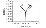
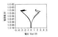
- FIG. 14 is an IV characteristic diagram in Experimental Example 2-4 of the present disclosure.
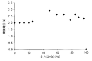
- It is a characteristic view showing the relationship between Si / (Si + Ge) ratio and threshold voltage.
- FIG. 14 is an IV characteristic diagram in Experimental Example 4-1 of the present disclosure. It is IV characteristic figure in Experimental example 4-3 of this indication. It is IV characteristic figure in Experimental example 4-5 of this indication. It is IV characteristic figure in Experimental example 4-6 of this indication. It is IV characteristic figure in Experimental example 5-1 of this indication. It is IV characteristic figure in Experimental example 5-2 of this indication.
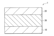
- FIG. 1 illustrates a cross-sectional configuration of a switch element 1 according to an embodiment of the present disclosure.
- the switch element 1 selectively operates, for example, an arbitrary storage element (storage element 2Y; FIG. 3) among a plurality of arranged in the memory cell array 2 having a so-called cross-point array structure shown in FIG. Is for.
- the switch element 1 (switch element 2X; FIG. 3) is connected in series to the memory element 2Y (specifically, the memory layer 40), and the lower electrode 10 (first electrode), the switch layer 30 and the upper electrode 20 ( 2nd electrode) in this order.
- the lower electrode 10 is a wiring material used in a semiconductor process, such as tungsten (W), tungsten nitride (WN), titanium nitride (TiN), copper (Cu), aluminum (Al), molybdenum (Mo), tantalum (Ta). ), Tantalum nitride (TaN), silicide, and the like.
- the lower electrode 10 is made of a material that may cause ion conduction in an electric field such as Cu
- the surface of the lower electrode 10 made of Cu or the like is made of W, WN, titanium nitride (TiN), TaN, or the like. You may make it coat
- the switch layer 30 in the present embodiment is made of an amorphous material containing germanium (Ge) and nitrogen (N) or oxygen (O). About several percent of nitrogen or oxygen contained in the switch layer 30 may be contained. Specifically, nitrogen preferably includes, for example, 3 atomic percent or more and 40 atomic percent or less, and oxygen preferably includes, for example, 3 atomic percent or more and 55 atomic percent or less. As a result, the switch layer 30 has a negative resistance characteristic in which the apparent resistance value becomes negative at a certain threshold voltage or higher, and the voltage applied to the switch element 1 exceeds a certain value (switching threshold voltage). Current will flow several orders of magnitude.
- the switch layer 30 preferably contains any one or more of boron (B), carbon (C), and silicon (Si) as additive elements. By using these additive elements, the current value in the off state (off current value) is reduced, and the on / off ratio of the memory cell can be further increased.
- the film thickness of the switch layer 30 is not particularly limited, but is preferably 50 nm or less, for example.
- the switch layer 30 may contain elements other than these in the range which does not impair the effect of this indication.
- a known semiconductor wiring material can be used similarly to the lower electrode 10, but a stable material that does not react with the switch layer 30 even after post-annealing is preferable.
- the switch element 1 of the present embodiment has a high resistance value in the initial state (high resistance state (off state)), and is low (low resistance state (on state)) at a certain voltage (switching threshold voltage) when a voltage is applied. ) And negative resistance characteristics. Further, the switch element 1 returns to the high resistance state when the applied voltage is lowered below the switching threshold voltage or when the voltage application is stopped, and the on state is not maintained. That is, the switch element 1 has a phase change (amorphous phase (amorphous phase)) of the switch layer 30 by applying a voltage pulse or a current pulse through a lower electrode 10 and an upper electrode 20 from a power supply circuit (pulse applying means) (not shown). ) And crystal phase).
- the capacity of the memory is increased as shown in FIG. 3 in which a memory cell in which a memory element and a switch element are stacked is arranged in the vicinity of the crossing point between intersecting wirings. This can be realized by adopting an array structure.
- the current value that flows when the half-select voltage V / 2 is applied to the memory cell is equal to the current value when the voltage V / 2 is applied to the memory element.
- the memory cell is composed of a memory element and a switch element, specifically, a structure in which the memory cells are connected in series with each other
- the half-select voltage V / 2 is applied to the memory cell
- the flowing current value becomes smaller if the resistance value of the switch element is larger than the resistance value of the memory element. This is because most of the applied voltage is divided by the switch element, that is, the leakage current (off) flowing through the half-selected cell is reduced.
- the selection voltage V is applied to the memory cell, if the selection voltage V is larger than the threshold voltage of the switch element, the resistance value of the switch element decreases (switches) and current flows (ON). ), A voltage is applied to the memory elements connected in series.
- operations such as writing or erasing can be performed by changing the resistance value of the memory element.
- the memory element and the switch element it is possible to increase the selection ratio (on / off ratio) of the memory cell and selectively operate any memory cell.
- the above-mentioned ovonic threshold switch using a chalcogenide material has a negative resistance characteristic or an S-type negative resistance characteristic in which the apparent resistance value becomes negative at a certain threshold voltage (switching threshold voltage) or more, and therefore the on / off ratio Therefore, it can be said that it is suitable as a switch element used in a memory having a plurality of memory cells such as a cross-point type memory.
- the current-voltage (IV) characteristic of a switch element having negative resistance characteristics is obtained by measuring a current when a voltage is applied to the switch element and a load resistance having a known resistance value and the applied voltage is increased. It can be examined by subtracting the voltage related to the load resistance. Normally, when the applied voltage is increased with respect to the switch element, the current value also increases. However, in a switching element having a negative resistance, the voltage decreases conversely at a certain threshold voltage or higher, and only the current increases after decreasing to a voltage called a holding voltage, and the apparent resistance value becomes negative. This negative resistance characteristic can also be observed by measuring the voltage when the current value is increased with respect to the switch element.
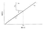
- FIG. 2A shows IV characteristics of a general memory element.
- the resistance value changes from a high off state (A) to a low resistance state (B) when the threshold voltage (V 0 ) is reached, and the on state (C). become.
- the applied current is decreased, the voltage of the resistance value decreases while maintaining the ON state (D).
- the memory element has a hysteresis characteristic that maintains the changed resistance value even when the applied voltage is lowered.
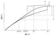
- FIG. 2B shows a change in voltage applied when the current applied to the switch element (X 0 ) having negative resistance characteristics and the switch element (Y 0 ) not having negative resistance characteristics is changed. is there.
- the vertical axis represents the current value in logarithm.
- FIG. 2C shows a memory cell (X, Y) in which the memory element having the IV characteristic shown in FIG. 2A and the switch element (X 0 , Y 0 ) having the characteristic chart shown in FIG. 2B are connected in series. And the IV characteristics thereof.
- a certain voltage threshold voltage
- the switching threshold voltage of the memory cell is set as a selection operation voltage V (Vx, Vy; on), and half of the voltage is set as a half selection voltage V / 2 ((V / 2) x, (V / 2) y; off).
- V / 2 half selection voltage
- the memory cell (X) using the switch element having the negative resistance characteristic is more memory cell using the switch element having no negative resistance characteristic. It can be seen that the on / off ratio is larger than (Y). This is because, when a voltage equal to or higher than the threshold voltage of the switch element is applied to the switch element, the voltage value applied to the switch element decreases due to the negative resistance characteristic, and the partial voltage applied to the memory element increases accordingly. It depends. That is, the memory element can be switched with a smaller applied voltage V, and the half-select voltage V / 2 is also reduced, so that the leakage current when the memory cell is half-selected can be reduced.
- the switch element having the negative resistance characteristic can improve the on / off ratio of the memory cell as compared with the switch element not having the negative resistance characteristic. Further, it is possible to reduce the leakage current flowing through the non-selected (or half-selected) memory cell. For this reason, it is suitable as a switching element for a memory having a plurality of memory cells, such as a cross-point type memory, and the capacity can be increased by further increasing the number of memory cells.
- a switch element using a chalcogenide material having a negative resistance characteristic has a problem that resistance to a semiconductor process used when manufacturing a cross-point type memory or the like is low. Specifically, since the chemical stability is low, there is a concern about damage during the miniaturization process due to etching or the like, and state stability in a high temperature process because of a relatively low melting point.
- the switch layer 30 is made of an amorphous material containing germanium (Ge) and nitrogen (N) or oxygen (O).
- An amorphous material containing germanium (Ge) and nitrogen (N) or oxygen (O) has a high affinity for a semiconductor process and is a relatively chemically and thermally stable material. For this reason, it becomes possible to easily use a miniaturization process such as etching or a high temperature process.
- the switch layer 30 is made of an amorphous material containing germanium (Ge) and nitrogen (N) or oxygen (O) that has high affinity for a semiconductor process. I made it. This improves the chemical and thermal stability of the semiconductor process used during manufacturing and improves the reliability. Thus, a storage device with high capacity and high reliability can be provided.
- the storage device (memory) can be configured by arranging a large number of storage elements 2Y to be described later, for example, in a column or matrix form.
- the switch element 1 of the present disclosure is connected in series with the storage element 2Y as the switch element 2X, thereby configuring the memory cell 2A.
- the memory cell 2A is connected to a sense amplifier, an address decoder, a write / erase / read circuit, and the like via wiring.
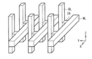
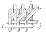
- FIG. 3 shows an example of a so-called cross-point array type storage device (memory cell array 2) in which memory cells 2A are arranged at intersections (cross points) between intersecting wirings.
- memory cell array 2 each memory cell 2 ⁇ / b> A extends in the Y-axis direction, and extends in the X-axis direction with a wiring (for example, a bit line; BL (row line)) corresponding to the lower electrode 10.
- a wiring for example, a word line; WL (vertical line)
- the floor area per unit cell can be reduced, and the capacity can be increased.
- a higher-density and larger-capacity memory can be realized by forming a three-dimensional structure in which unit structures composed of bit lines, memory cells 2A, and word lines are stacked in the Z-axis direction.
- the bit line or the word line may be shared by the upper and lower memory cells.
- an interlayer insulating film (not shown) may be provided between the stacked unit structures composed of the bit line, the memory cell 2A, and the word line.
- the memory element 2Y constituting the memory cell 2A has, for example, a lower electrode, a memory layer 40, and an upper electrode in this order.
- the memory layer 40 is configured, for example, by a laminated structure in which the resistance change layer 42 and the ion source layer 41 are laminated from the lower electrode side or a single layer structure of the resistance change layer 42.
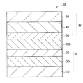
- an intermediate electrode 50 (third electrode) is provided between the switch layer 30 and the storage layer 40, and the intermediate electrode 50 includes an upper electrode of the switch element 2X and a lower electrode of the storage element 2Y.
- the memory cell 2A includes a switch layer 30, an intermediate electrode 50, a resistance change layer 42, and an ion source layer 41 between the lower electrode 10 and the upper electrode 20, as shown in FIG. It has the structure laminated
- the lower electrode 10 and the upper electrode 20 in the memory cell array 2 may be a bit line (BL) and a word line (WL), respectively, or may be connected to the bit line (BL) and the word line (WL).
- the lower electrode 10 and the upper electrode 20 may be formed so as to be sandwiched.
- the switch element 2X and the storage element 2Y illustrated in FIG. 3 correspond to the switch layer 30 and the storage layer 40, respectively.
- the intermediate electrode 50 is omitted and designated.
- the memory layer 40 may be a so-called resistance change type storage element (memory element) having a configuration such as a laminated structure of the ion source layer 41 and the resistance change layer 42 as described above.
- a resistance change memory made of a transition metal oxide, PCM (phase change memory) or MRAM (magnetoresistance change memory) may be used.
- the ion source layer 41 includes a movable element that forms a conduction path in the resistance change layer 42 by application of an electric field, for example, a transition metal element (Group 4 to Group 6) and a chalcogen element. For this reason, the ion source layer 41 has high chemical stability and heat resistance.
- the movable element include transition metal elements such as Cu and Al.
- manganese (Mn), cobalt (Co), iron (Fe), nickel (Ni), platinum (Pt), Si, etc., oxygen (O), and nitrogen (N) may be included.
- the resistance change layer 42 is made of, for example, an oxide or nitride of a metal element or a nonmetal element, and its resistance value changes when a predetermined voltage is applied between the lower electrode 10 and the upper electrode 20. Is. Specifically, when a voltage is applied between the lower electrode 10 and the upper electrode 20, the transition metal element contained in the ion source layer 41 moves into the resistance change layer 42 to form a conduction path, and the resistance The change layer 42 has a low resistance. Alternatively, structural defects such as oxygen defects and nitrogen defects are generated in the resistance change layer 42 to form a conduction path, and the resistance change layer 42 is reduced in resistance. Further, by applying a reverse voltage, the conduction path is cut or the conductivity is changed. As a result, the resistance change layer 42 is increased in resistance.
- the metal element and the non-metal element included in the resistance change layer 42 do not necessarily have to be in an oxide state, and may be in a state in which a part thereof is oxidized.
- the initial resistance value of the resistance change layer 42 only needs to realize an element resistance of, for example, several M ⁇ to several hundred G ⁇ , and the optimum value varies depending on the size of the element and the resistance value of the ion source layer 41.
- the film thickness is preferably about 1 nm to 10 nm, for example.
- the intermediate electrode 50 is not particularly limited as long as the intermediate electrode 50 is an inactive material that hardly causes oxidation-reduction reactions such as dissolution / precipitation of ions and movement of ions into the switch layer 30 and the ion source layer 41 containing chalcogenide by application of an electric field. .
- the intermediate electrode 50 is not necessarily provided, and may be omitted as appropriate.
- a voltage or current pulse in a “positive direction” (for example, a negative potential on the first electrode side and a positive potential on the second electrode side) is applied to the element in the initial state (high resistance state).
- the metal element for example, transition metal element
- the metal element contained in the ion source layer is ionized and diffuses in the memory layer (for example, in the resistance change layer), or oxygen ions move in the resistance change layer. Oxygen defects are generated.
- a low resistance portion (conductive path) having a low oxidation state is formed in the memory layer, and the resistance of the resistance change layer is lowered (recording state).
- the metal ions in the resistance change layer are ionized. Movement into the source layer or oxygen ions from the ion source layer reduces oxygen defects in the conduction path portion. As a result, the conduction path containing the metal element disappears, and the resistance of the variable resistance layer becomes high (initial state or erased state).
- the memory layer 40 is formed of a single layer of the resistance change layer 42, defects are generated by a case where a positive voltage (or current pulse) is applied and an electric field applied to the resistance change layer 42.
- a voltage pulse is applied in the negative direction, the defect is repaired by the movement of oxygen ions and nitrogen ions in the resistance change layer.
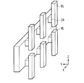
- the cross-point array type memory cell array 2 is not limited to the structure shown in FIG.
- WL may extend in the X-axis direction
- BL may extend in the Z-axis direction
- FIG. 5B a structure may be adopted in which the memory cells 2A are respectively provided on both surfaces of intersections of WL and BL extending in the X-axis direction and the Z-axis direction, respectively.
- BL may extend in the X-axis direction and WL may extend in the Z-axis direction.
- WL and BL do not necessarily have to be extended in one direction.
- a part of WL may extend in the X-axis direction or the Y-axis direction.
- WL may be continuously refracted from the X-axis direction to the Y-axis direction.
- the WL may be common to a plurality of BLs.
- the memory device using the resistance change type memory element 2Y has been described as an example.
- the present invention is not limited to this and can be applied to various memory devices.
- any memory form such as a PROM that can be written only once, an EEPROM that can be electrically erased, or a so-called RAM that can be written / erased / reproduced at high speed can be applied.
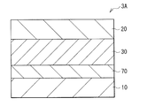
- FIG. 6A shows an example of a cross-sectional configuration of a switch element 3A as a modified example of the present disclosure according to the above-described embodiment.
- the switch element 3A is different from the switch element 1 in that a high resistance layer 70 is provided in addition to the switch layer 30 between the lower electrode 10 and the upper electrode 20.
- a high resistance layer 70 is provided in addition to the switch layer 30 between the lower electrode 10 and the upper electrode 20.
- symbol is attached
- the high resistance layer 70 has, for example, higher insulating properties than the switch layer 30 and includes, for example, an oxide or nitride of a metal element or a nonmetal element, or a mixture thereof.
- the switch element 3 in this modification should just contact
- FIG. an example in which the high resistance layer 70 is provided on the lower electrode 10 side with respect to the switch layer 30 is shown, but the present invention is not limited thereto, and the high resistance layer 70 may be provided on the upper electrode 20 side with respect to the switch layer 30.
- the switch layer 30 may be sandwiched between the high-resistance layers 70A and 70B on both sides of the lower electrode 10 and the upper electrode 20, that is, the switch layer 30.
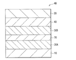
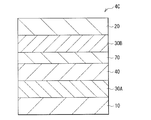
- the switch layer 30 may be two layers (switch layers 30A and 30B), and the high resistance layer 70 may be provided between the switch layer 30A and the switch layer 30B.
- a multilayer structure in which a plurality of sets of switch layers and high resistance layers 70 are laminated may be employed.
- the memory cells 4 in which the switch elements 3A to 3C of the present modification and the memory element 2Y are connected in series are, for example, as shown in FIGS. 7A to 7C.
- FIGS. 7A to 7C use the switch element 3C shown in FIG. 6C.
- a memory cell 4A shown in FIG. 7A is obtained by stacking a memory layer 40 via an intermediate electrode 50 on the upper electrode side of the switch layer 30B. In the memory cell 4B shown in FIG. 7B, the intermediate electrode 50 is omitted.
- the memory cell 4C shown in FIG. 7C has a memory layer provided between the switch layer 30A and the high resistance layer 70.
- the stacking order of the switch layer 30 (switch layers 30A and 30B), the high resistance layer 70, and the memory layer 40 is not particularly limited.
- the storage device in the present modification is the same when the so-called PCM and MRAM configurations are applied to the storage layer 40.
- Example 1 First, the lower electrode 10 made of TiN was cleaned by reverse sputtering. Next, a switch layer 30 made of Ge—Nx is formed to a thickness of 20 nm on TiN by reactive sputtering while flowing nitrogen into the film formation chamber, and then W is formed to a thickness of 30 nm to form the upper electrode. It was set to 20. Subsequently, after performing heat treatment and patterning at 320 ° C. for 2 hours, a switch element for measuring characteristics (Experimental Examples 1-1, 1 Resistance-1 Selector element) was manufactured by connecting fixed resistors in series.
- a switch element for characteristic measurement (Experimental Example 1-2) having a switch layer 30 made of Ge—Ox was manufactured using the same method except that oxygen was allowed to flow into the film formation chamber.
- the composition of each layer of Experimental Examples 1-1 and 1-2 is shown below in the order of “lower electrode / switch layer / upper electrode”.
- DC loop measurement was performed by changing the applied voltage Vin from 0V ⁇ 6V ⁇ 0V ⁇ ⁇ 6V ⁇ 0V, and the current change with respect to the voltage of only the switch element ( Resistance change) was examined.
- Example 1-1 TiN / Ge-Nx (20 nm) / W (30 nm)
- Example 1-2 TiN / Ge-Ox (30 nm) / W (30 nm)
- the horizontal axis represents the voltage Vsel applied to only the characteristic measuring switch element (the value obtained by subtracting the voltage applied to the series resistance from the applied voltage Vin), and the vertical axis represents the current value measured at each voltage Vsel.
- the applied voltage Vin is mainly divided into the switch layer 30 and the series resistance.
- Example 1-1 the on state where a large amount of current flows was not maintained and there was no hysteresis. Furthermore, it has been found that it has a symmetric characteristic with respect to the minus ( ⁇ ) side applied voltage. It was found from FIG. 9 that these characteristics also have Experimental Example 1-2 having the switch layer 30 made of Ge—Ox. That is, it was found that the switch element 1 including the switch layer 30 made of a material in which germanium and nitrogen or germanium and oxygen are combined has negative resistance characteristics and switch characteristics.
- Example 2 Next, except that the switch layer 30 is made of SiGe-Nx and the flow rate composition of the gas to be introduced at the time of film formation is changed, the following sample (Experimental Example 2-1 to 2-13) was produced.
- the gas flow rate composition in each sample is as follows: the argon (Ar) gas flow rate is 75 sccm, the nitrogen (N 2 ) flow rate is 10 sccm, and the ratio of Si / (Si + Ge) is 0%, 7%, 13%, 20%, 25%, 49%, 59%, 69%, 78%, 85%, 90%, 97%, and 100%.
- the composition of each layer in Experimental Examples 2-1 to 2-13 is shown below in the order of “lower electrode / switch layer / upper electrode”.
- the film thickness of the switch layer 30 and the upper electrode 20 in each sample is 30 nm.
- the DC loop measurement was performed in the same manner as in Experiment 1, and the current change (resistance change) with respect to the voltage was examined.
- FIGS. 10 to 13 show IV characteristics of Experimental Examples 2-2, 2-6, 2-11, and 2-13, respectively. From FIG. 13, it was found that when the switch layer 30 is composed of only Si—Nx, switch characteristics cannot be obtained. On the other hand, from FIGS. 10 and 11, by adding Si to the switch layer 30 made of Ge—Nx, the off-current value is reduced as compared with FIG. 9, and the difference from the current value after switching is different. It became larger and the resistance change became clearer. That is, it has been found that the switch layer 30 can further improve the switch characteristics by adding not only Ge—Nx but also silicon (Si).
- FIG. 14 is a plot of the switching threshold voltage against the Si / (Si + Ge) ratio in Experimental Examples 2-1 to 2-13. Note that the switching threshold voltage when the switch characteristic is not provided is 0. From FIG. 14, it was found that Si has a switching threshold voltage, a negative resistance characteristic, and a switching characteristic when added to the switching layer 30 in a range of 0% to 97% with respect to Si + Ge. In other words, it can be seen that the Si—Nx film has negative resistance characteristics and switching characteristics when Ge is contained in an amount of 3% or more. That is, in the switch element 1 including the switch layer 30 composed of silicon, germanium, and nitrogen, negative resistance characteristics and switch characteristics are obtained when the Si content with respect to Si + Ge is 0% or more and 97% or less, and more preferably.
- the Si content relative to Si + Ge is 7% or more and 90% or less.
- negative resistance characteristics and switching characteristics can be obtained when the ratio of Ge to Ge + Si is 3% or more and 100% or less, and more preferably, Ge is 10% or more and 93% or less. .
- the following samples (Experimental Examples 3-1 to 3-9) were prepared using the above method.
- the gas flow rate composition in each sample was an argon (Ar) gas flow rate of 75 sccm and a nitrogen (N 2 ) flow rate of 0, 2 , 5, 7, 10, 15, 20, 25, 30 sccm.
- the gas flow rate composition is argon (Ar) gas flow rate of 75 sccm and oxygen (O 2 ) flow rate of 0,1.
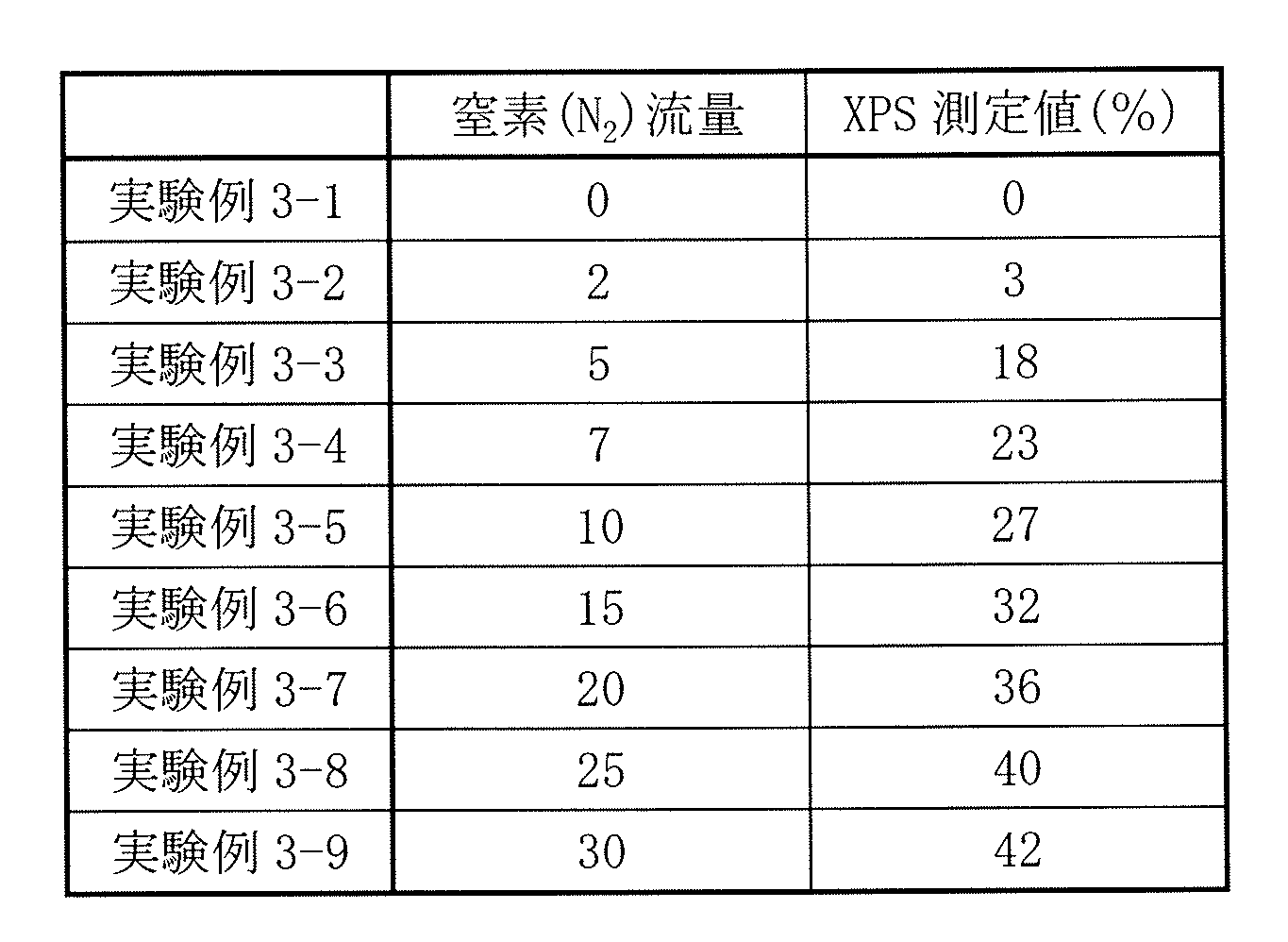
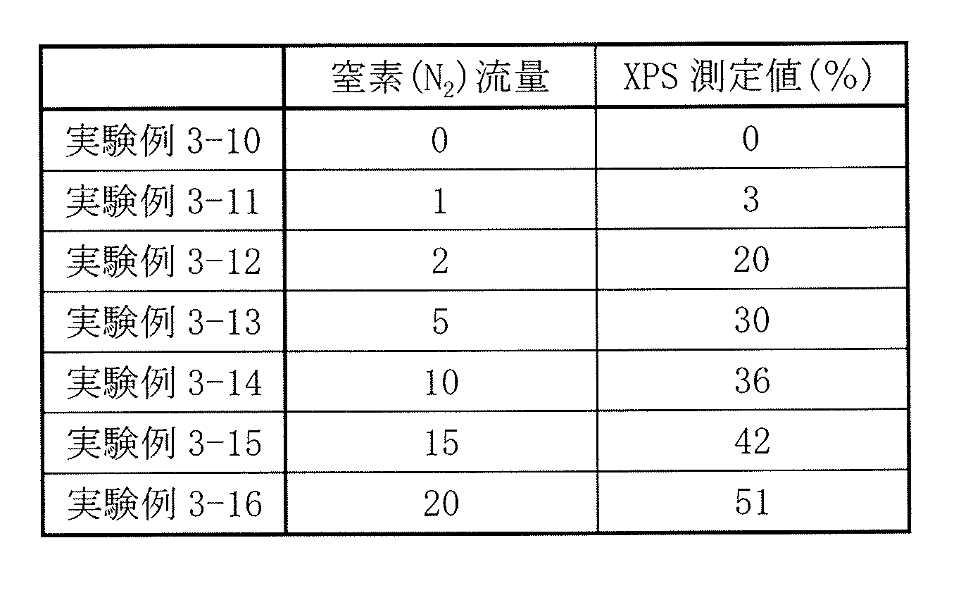
- Tables 1 and 2 summarize the results of measuring the N content or O content in these samples using XPS.
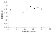
- DC loop measurement was performed on these samples in the same manner as in Experiment 1, the current change with respect to voltage (resistance change) was examined, and the change in switching threshold voltage with respect to the content of each nitrogen (N) or oxygen (O). The results are shown in FIG. 15 (SiGe—Nx) and FIG. 16 (SiGe—Ox).
- the switching threshold voltage exists, and it has negative resistance characteristics and switching characteristics in which the current value changes rapidly upon voltage application. all right. Further, when the oxygen content was 0 atomic% or 60 atomic%, there was no switching threshold voltage, and no switching characteristics were observed. Therefore, it was found that the oxygen content at which the negative resistance characteristic and the switching characteristic can be obtained in the switch layer 30 made of SiGe—Ox is preferably 3 atomic% or more and 55 atomic% or less.
- Example 4 As Experiment 4, using the same method as in Experiment 1, GeNx containing carbon (C) and / or boron (B) as an additive element while flowing argon gas and nitrogen gas into the film forming chamber.
- the switch layer 30 made of was formed to prepare samples (Experimental examples 4-1 to 4-3).
- a switch layer 30 made of GeOx containing carbon (C) or boron (B) as an additive element or both is formed by flowing oxygen gas instead of nitrogen gas into the film formation chamber, A sample (Experimental Example 4-4) was produced.
- Example 4-6 The sample used (Experimental Example 4-6) was produced.
- the composition ratio of the switch layer 30 in each sample is shown below.
- the film thickness of the switch layer 30 and the upper electrode 20 is 30 nm, respectively.
- the DC loop measurement was performed in the same manner as in Experiment 1, and the current change (resistance change) with respect to the voltage was examined.
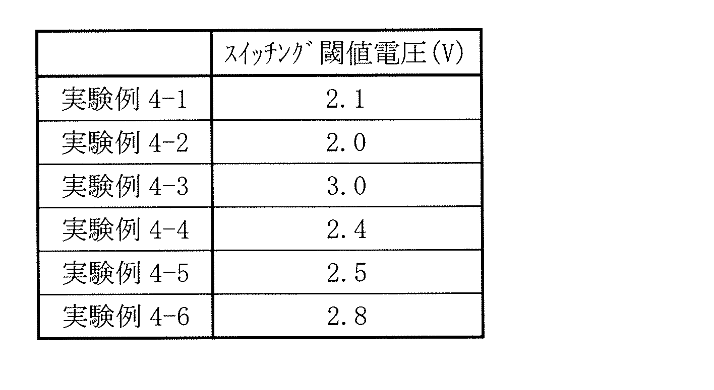
- 17 to 20 show IV characteristics in Experimental Examples 4-1, 4-3, 4-5, and 4-6, respectively, and Table 3 summarizes the switching threshold voltage in each sample. It is.
- Example 4-1 TiN / C20-Ge80-Nx / W (Experimental example 4-2) TiN / B25-Ge85-Nx / W (Experimental example 4-3) TiN / B56-C-14-Ge30-Nx / W (Experimental Example 4-4) TiN / B56-C-14-Ge30-Ox / W (Experimental example 4-5) TiN / Si20-C20-Ge60-Nx / W (Experimental example 4-6) TiN / B5-Si47.5-Ge47.5-Nx / W
- the switch layer 30 has a lower current value when turned off, and the difference from the current value after the switching threshold voltage becomes clear. It was. In addition, the negative resistance characteristics became clear. Comparing Experimental Example 4-1 and Experimental Example 4-3, further using boron as an additional element further reduces the off-state current value and further increases the difference from the current value after the switching threshold voltage. I found out that That is, it was found that the switch characteristics of the switch layer 30 can be improved by using not only silicon used in Experiment 2 but also boron or carbon as the additive element used in the switch layer 30.
- the negative resistance characteristics and the switch characteristics can be improved even when two or more silicon, boron, and carbon are used as additive elements.
- Ge—Nx and Ge—Ox constituting the switch layer of the present disclosure can be used by adding one or more of silicon, boron, and carbon as additive elements in the off state. It has been found that the switch characteristics can be further improved, for example, by reducing the leakage current.
- silicon and carbon are considered to be similar in nature because they are the same element and can have the same valence. It can be inferred that mixing the combination of carbon, germanium, and nitrogen provides the same effect within the same range as silicon, germanium, and nitrogen. From this, the preferable ratio of carbon to be added to the switch layer 30 is the same as that of silicon. When germanium and carbon are 100%, the switch characteristics can be obtained when the ratio of germanium is 3 to 100%. Is considered to be 10 to 93% germanium.
- the valence of boron is 3, it is estimated that the effect of improving the characteristics can be obtained even if the ratio to germanium is more than silicon or carbon.
- part or all of silicon or carbon is substituted with boron in the composition range of silicon (or carbon).
- 4/3 boron is substituted.
- the switching characteristics can be obtained when the germanium ratio is 2 to 100%, but it is more preferable that germanium is 8 to 91%.
- each additive element of silicon, carbon, and boron is effective in improving the characteristics, even if two or more of these are combined with simultaneous germanium and nitrogen or oxygen, the effect of improving the characteristics by the added elements can be obtained.
- the ratio of each additive element and germanium if the ratio of elements other than nitrogen or oxygen is at least 3% germanium, the switch characteristic is obtained.
- the germanium ratio is 10 to 91%, it depends on the additive element. It can be estimated that the effect of improving the characteristics appears more clearly.
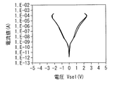
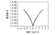
- Example 5 First, as Experimental Example 5-1, the lower electrode 10 made of TiN was cleaned by reverse sputtering. Next, a switch layer 30A made of Ge—Nx is formed on the TiN film with a thickness of 10 nm by reactive sputtering while flowing nitrogen into the film formation chamber, and then a SiNx film is formed with a thickness of 5 nm. A resistance layer 70 was formed. Further, a switch layer 30A made of Ge—Nx was formed to a thickness of 10 nm on the high resistance layer 70, and then W was formed to a thickness of 30 nm to form the upper electrode 20.
- composition ratio of each layer of Experimental Example 5-1 and Experimental Example 5-2 is defined as “lower electrode / switch layer / high resistance layer / switch layer / upper electrode” (Experimental example 5-1), “lower electrode / High resistance layer / switch layer / high resistance layer / upper electrode ”(Experimental example 5-2).
- the IV characteristics of Experimental Example 5-1 and Experimental Example 5-2 are shown in FIGS.
- the present technology can take the following configurations.
- the switch layer includes at least one of boron (B), carbon (C), and silicon (Si) as an additive element.
- nitrogen (N) contained in the switch layer is not less than 3 atom% and not more than 40 atom%.
- the switch layer changes to a low resistance state by setting the applied voltage to a predetermined threshold voltage or higher, and changes to a high resistance state again by reducing the applied voltage to the threshold voltage or lower.
- (1) to (7) The switch element according to any one of the above. (9) Any one of (1) to (8) above, wherein a high resistance layer containing an oxide or nitride of a metal element or a nonmetal element is provided between the first electrode and the second electrode. Switch element according to one. (10) The switch element according to (9), wherein the high resistance layer is provided on at least one surface of the switch layer on the first electrode side and the second electrode side.
- a plurality of memory cells including a memory element and a switch element connected to the memory element, wherein the switch element includes a first electrode, a second electrode disposed to face the first electrode, and the first electrode And a switch layer provided between the second electrode and the second electrode, wherein the switch layer includes an amorphous material composed of at least germanium (Ge) and nitrogen (N) or oxygen (O) .
- the storage element includes a storage layer between the first electrode and the second electrode of the switch element.
- the storage layer and the switch layer are stacked via a third electrode between the first electrode and the second electrode.
- the memory layer includes an ion source layer including at least one chalcogen element selected from tellurium (Te), sulfur (S), and selenium (Se), and a resistance change layer.
- the storage device according to 13).
- the memory cells (11) to (14) having a plurality of row lines and a plurality of column lines, wherein the memory cells are arranged in the vicinity of intersection regions of the plurality of row lines and the plurality of column lines.
- the storage device according to any one of the above.
- Any one of (12) to (15), wherein the memory layer is any one of a resistance change layer made of a transition metal oxide, a phase change memory layer, and a magnetoresistance change memory layer.
- the storage device according to one.
Landscapes
- Chemical & Material Sciences (AREA)
- Engineering & Computer Science (AREA)
- Crystallography & Structural Chemistry (AREA)
- Materials Engineering (AREA)
- Computer Hardware Design (AREA)
- Semiconductor Memories (AREA)
- Physical Vapour Deposition (AREA)
Abstract
Description
1.実施の形態(電極間にGeとNあるいはOとを含むスイッチ層を設けた例)
1-1.スイッチ素子
1-2.記憶装置
2.変形例(電極間に高抵抗層を追加した例)
3.実施例
(1-1.スイッチ素子)
図1は、本開示の一実施の形態に係るスイッチ素子1の断面構成を表したものである。このスイッチ素子1は、例えば、図3に示した、所謂クロスポイントアレイ構造を有するメモリセルアレイ2において複数配設されたうちの任意の記憶素子(記憶素子2Y;図3)を選択的に動作させるためのものである。スイッチ素子1(スイッチ素子2X;図3)は、記憶素子2Y(具体的には記憶層40)に直列に接続されており、下部電極10(第1電極)、スイッチ層30および上部電極20(第2電極)をこの順に有するものである。
記憶装置(メモリ)は、後述する記憶素子2Yを多数、例えば列状やマトリクス状に配列することにより構成することができる。このとき、本開示のスイッチ素子1は、スイッチ素子2Xとして、記憶素子2Yと直列に接続されており、これによりメモリセル2Aを構成している。メモリセル2Aは、配線を介してセンスアンプ,アドレスデコーダおよび書き込み・消去・読み出し回路等に接続される。
図6Aは、上記実施の形態に係る本開示の変形例としてのスイッチ素子3Aの断面構成の一例を表したものである。このスイッチ素子3Aは、下部電極10と上部電極20との間に、スイッチ層30に加えて高抵抗層70が設けられた点が、上記スイッチ素子1とは異なる。なお、上記実施の形態と同一の構成要素については同一符号を付してその説明は省略する。
以下、本開示の具体的な実施例について説明する。
まず、TiNよりなる下部電極10を逆スパッタによってクリーニングした。次に、成膜チャンバー内に窒素を流しながらリアクティブスパッタによってTiN上にGe-Nxからなるスイッチ層30を20nmの膜厚で成膜したのち、Wを30nmの膜厚で形成して上部電極20とした。続いて、320℃、2時間の熱処理およびパターニングを行ったのち、固定抵抗を直列に接続することによって特性測定用のスイッチ素子(実験例1-1,1Resistance-1Selector素子)を作製した。また、成膜チャンバー内に酸素を流した以外は同様の方法を用いて、Ge-Oxからなるスイッチ層30を有する特性測定用のスイッチ素子(実験例1-2)を作製した。実験例1-1,1-2の各層の組成については、「下部電極/スイッチ層/上部電極」の順に以下に示す。これら実験例1-1,1-2に対して、印加電圧Vinを、0V→6V→0V→-6V→0Vのように変化させたDCループ測定を行い、スイッチ素子のみの電圧に対する電流変化(抵抗変化)を調べた。
(実験例1-1)TiN/Ge-Nx(20nm)/W(30nm)
(実験例1-2)TiN/Ge-Ox(30nm)/W(30nm)
次に、スイッチ層30をSiGe-Nxから構成し、その成膜時において流入させるガスの流量組成を変えた以外は、実験1と同様の方法を用いて以下のサンプル(実験例2-1~2-13)を作製した。各サンプルにおけるガスの流量組成は、アルゴン(Ar)ガス流量を75sccm、窒素(N2)流量を10sccmとし、Si/(Si+Ge)の割合が、それぞれ0%,7%,13%,20%,25%,49%,59%,69%,78%,85%,90%,97%,100%となるようにした。なお、実験例2-1~2-13の各層の組成については、「下部電極/スイッチ層/上部電極」の順に以下に示す。また、各サンプルにおけるスイッチ層30および上部電極20の膜厚は、それぞれ30nmである。これらサンプルに対して、実験1と同様にDCループ測定を行い、電圧に対する電流変化(抵抗変化)を調べた。
(実験例2-1)TiN/Ge-Nx/W
(実験例2-2)TiN/Si7-Ge93-Nx/W
(実験例2-3)TiN/Si13-Ge87-Nx/W
(実験例2-4)TiN/Si20-Ge80-Nx/W
(実験例2-5)TiN/Si25-Ge75-Nx/W
(実験例2-6)TiN/Si49-Ge51-Nx/W
(実験例2-7)TiN/Si59-Ge41-Nx/W
(実験例2-8)TiN/Si69-Ge31-Nx/W
(実験例2-9)TiN/Si78-Ge22-Nx/W
(実験例2-10)TiN/Si85-Ge15-Nx/W
(実験例2-11)TiN/Si90-Ge10-Nx/W
(実験例2-12)TiN/Si97-Ge3-Nx/W
(実験例2-13)TiN/Si-Nx/W
次に、実験3として、スイッチ層30を構成するSiとGeとの比率をSi:Ge=6:4とし、その成膜時において流入させるガスの流量組成を変えた以外は、実験1と同様の方法を用いて以下のサンプル(実験例3-1~3-9)を作製した。各サンプルにおけるガスの流量組成は、アルゴン(Ar)ガス流量を75sccm、窒素(N2)流量を0,2,5,7,10,15,20,25,30sccmとした。同様に、スイッチ層30を構成するSiとGeとの比率をSi:Ge=5:5とし、ガスの流量組成は、アルゴン(Ar)ガス流量を75sccm、酸素(O2)流量を0,1,2,5,10,15,20sccmとしてサンプル(実験例3-10~3-16)を作製した。表1,2は、これらサンプルにおけるN含有量あるいはO含有量をそれぞれXPSを用いて測定し、まとめたものである。また、これらサンプルに対して、実験1と同様にDCループ測定を行い、電圧に対する電流変化(抵抗変化)を調べ、各窒素(N)あるいは酸素(O)の含有量に対するスイッチング閾値電圧の変化を図15(SiGe-Nx)および図16(SiGe-Ox)に示した。
次に、実験4として、上記実験1と同様の方法を用い、成膜チャンバー内にアルゴンガスおよび窒素ガスを流しつつ、添加元素として炭素(C)あるいはホウ素(B)、またはその両方を含むGeNxからなるスイッチ層30を成膜し、サンプル(実験例4-1~4-3)を作製した。また、同様に、窒素ガスの代わりに酸素ガスを成膜チャンバー内に流して、添加元素として炭素(C)あるいはホウ素(B)、またはその両方を含むGeOxからなるスイッチ層30を成膜し、サンプル(実験例4-4)を作製した。さらに、アルゴンガスおよび窒素ガスを成膜チャンバー内に流して、添加元素としてケイ素(Si),炭素(C)を用いたサンプル(実験例4-5)およびケイ素(Si),ホウ素(B)を用いたサンプル(実験例4-6)を作製した。各サンプルにおけるスイッチ層30の組成比を以下に示す。なお、スイッチ層30および上部電極20の膜厚は、それぞれ30nmである。これらサンプルに対して、実験1と同様にDCループ測定を行い、電圧に対する電流変化(抵抗変化)を調べた。図17~図20は、それぞれ、実験例4-1,4-3,4-5,4-6におけるIV特性を表したものであり、表3は、各サンプルにおけるスイッチング閾値電圧をまとめたものである。
(実験例4-1)TiN/C20-Ge80-Nx/W
(実験例4-2)TiN/B25-Ge85-Nx/W
(実験例4-3)TiN/B56-C-14-Ge30-Nx/W
(実験例4-4)TiN/B56-C-14-Ge30-Ox/W
(実験例4-5)TiN/Si20-C20-Ge60-Nx/W
(実験例4-6)TiN/B5-Si47.5-Ge47.5-Nx/W
まず、実験例5-1として、TiNよりなる下部電極10を逆スパッタによってクリーニングした。次に、成膜チャンバー内に窒素を流しながらリアクティブスパッタによってTiN上にGe-Nxからなるスイッチ層30Aを10nmの膜厚で成膜したのち、SiNx膜を5nmの膜厚に形成して高抵抗層70を形成した。更に、この高抵抗層70上に、Ge-Nxからなるスイッチ層30Aを10nmの膜厚で成膜したのち、Wを30nmの膜厚で形成して上部電極20とした。また、実験例5-2として、TiNよりなる下部電極10を逆スパッタによってクリーニングしたのち、TiN上にSiNx膜を10nmの膜厚に形成して高抵抗層70を形成した。次に、成膜チャンバー内にアルゴン(Ar)および窒素(N)あるいは酸素(O)を流しながらリアクティブスパッタによってGe-Nxからなるスイッチ層30を30nmの膜厚で成膜したのち、さらに、高抵抗層70Bを成膜したのち、Wを30nmの膜厚で形成して上部電極20とした。以下、上記実験1と同様の方法を用いてスイッチ素子3を作製した。以下に、実験例5-1および実験例5-2の各層の組成比を、「下部電極/スイッチ層/高抵抗層/スイッチ層/上部電極」(実験例5-1),「下部電極/高抵抗層/スイッチ層/高抵抗層/上部電極」(実験例5-2)の順に示す。また、実験例5-1および実験例5-2のIV特性を図21,図22に示す。
(実験例5-1)TiN/Si50-Ge50-Nx(10nm)/SiNx(5nm)/Si50-Ge50-Nx(10nm)/W(30nm)
(実験例5-2)TiN/SiNx(5nm)/Si50-Ge50-Nx(10nm)/SiNx(5nm)/W(30nm)
(1)第1電極および前記第1電極に対向配置された第2電極と、前記第1電極と前記第2電極との間に設けられたスイッチ層とを備え、前記スイッチ層は、少なくともゲルマニウム(Ge)と、窒素(N)あるいは酸素(O)とを含むアモルファス材料から構成されているスイッチ素子。
(2)前記スイッチ層は、添加元素として、ホウ素(B),炭素(C)およびケイ素(Si)のうちの少なくとも1種を含んでいる、前記(1)に記載のスイッチ素子。
(3)前記スイッチ層に含まれる窒素(N)は、3原子%以上40原子%以下である、前記(1)または(2)に記載のスイッチ素子。
(4)前記スイッチ層に含まれる酸素(O)は、3原子%以上55原子%以下である、前記(1)乃至(3)のうちのいずれか1つに記載のスイッチ素子。
(5)前記スイッチ層に含まれるケイ素(Si)に対するゲルマニウム(Ge)の含有量は、3%以上である、前記(2)乃至(4)のうちのいずれか1つに記載のスイッチ素子。(6)前記スイッチ層に含まれる前記添加元素に対するゲルマニウム(Ge)の含有量は、10%以上93%以下である、前記(2)乃至(4)のうちのいずれか1つに記載のスイッチ素子。
(7)前記スイッチ層の膜厚は50nm以下である、前記(1)乃至(6)のうちのいずれか1つに記載のスイッチ素子。
(8)前記スイッチ層は、印加電圧を所定の閾値電圧以上とすることにより低抵抗状態に、該閾値電圧以下に減少させることにより再び高抵抗状態に変化する、前記(1)乃至(7)のうちのいずれか1つに記載のスイッチ素子。
(9)前記第1電極および前記第2電極の間に、金属元素又は非金属元素の酸化物あるいは窒化物を含む高抵抗層を有する、前記(1)乃至(8)のうちのいずれか1つに記載のスイッチ素子。
(10)前記高抵抗層は、前記スイッチ層の前記第1電極側および前記第2電極側の少なくとも一方の面に設けられている、前記(9)に記載のスイッチ素子。
(11)記憶素子および前記記憶素子に接続されたスイッチ素子を含むメモリセルを複数備え、前記スイッチ素子は、第1電極および前記第1電極に対向配置された第2電極と、前記第1電極と前記第2電極との間に設けられたスイッチ層とを有し、前記スイッチ層は、少なくともゲルマニウム(Ge)と窒素(N)あるいは酸素(O)とからなるアモルファス材料を含んでいる記憶装置。
(12)前記記憶素子は前記スイッチ素子の前記第1電極および前記第2電極間に記憶層を有する、前記(11)に記載の記憶装置。
(13)前記記憶層および前記スイッチ層は前記第1電極と前記第2電極との間に第3電極を介して積層されている、前記(12)に記載の記憶装置。
(14)前記記憶層はテルル(Te),硫黄(S)およびセレン(Se)から選ばれる少なくとも1種のカルコゲン元素を含むイオン源層と、抵抗変化層とを含む、前記(12)または(13)に記載の記憶装置。
(15)複数の行ラインおよび複数の列ラインを有し、前記複数の行ラインと複数の列ラインとの各交差領域付近に前記メモリセルが配置されている、前記(11)乃至(14)のうちのいずれか1つに記載の記憶装置。
(16)前記記憶層は、遷移金属酸化物からなる抵抗変化層、相変化型メモリ層、磁気抵抗変化型メモリ層のいずれかである、前記(12)乃至(15)のうちのいずれか1つに記載の記憶装置。
Claims (16)
- 第1電極および前記第1電極に対向配置された第2電極と、前記第1電極と前記第2電極との間に設けられたスイッチ層とを備え、
前記スイッチ層は、少なくともゲルマニウム(Ge)と、窒素(N)あるいは酸素(O)とを含むアモルファス材料から構成されている
スイッチ素子。 - 前記スイッチ層は、添加元素として、ホウ素(B),炭素(C)およびケイ素(Si)のうちの少なくとも1種を含んでいる、請求項1に記載のスイッチ素子。
- 前記スイッチ層に含まれる窒素(N)は、3原子%以上40原子%以下である、請求項1に記載のスイッチ素子。
- 前記スイッチ層に含まれる酸素(O)は、3原子%以上55原子%以下である、請求項1に記載のスイッチ素子。
- 前記スイッチ層に含まれるケイ素(Si)に対するゲルマニウム(Ge)の含有量は、3%以上である、請求項2に記載のスイッチ素子。
- 前記スイッチ層に含まれる前記添加元素に対するゲルマニウム(Ge)の含有量は、10%以上93%以下である、請求項2に記載のスイッチ素子。
- 前記スイッチ層の膜厚は50nm以下である、請求項1に記載のスイッチ素子。
- 前記スイッチ層は、印加電圧を所定の閾値電圧以上とすることにより低抵抗状態に、該閾値電圧以下に減少させることにより再び高抵抗状態に変化する、請求項1に記載のスイッチ素子。
- 前記第1電極および前記第2電極の間に、金属元素又は非金属元素の酸化物あるいは窒化物を含む高抵抗層を有する、請求項1に記載のスイッチ素子。
- 前記高抵抗層は、前記スイッチ層の前記第1電極側および前記第2電極側の少なくとも一方の面に設けられている、請求項9に記載のスイッチ素子。
- 記憶素子および前記記憶素子に接続されたスイッチ素子を含むメモリセルを複数備え、
前記スイッチ素子は、
第1電極および前記第1電極に対向配置された第2電極と、前記第1電極と前記第2電極との間に設けられたスイッチ層とを有し、
前記スイッチ層は、少なくともゲルマニウム(Ge)と窒素(N)あるいは酸素(O)とからなるアモルファス材料を含んでいる
記憶装置。 - 前記記憶素子は前記スイッチ素子の前記第1電極および前記第2電極間に記憶層を有する、請求項11に記載の記憶装置。
- 前記記憶層および前記スイッチ層は前記第1電極と前記第2電極との間に第3電極を介して積層されている、請求項12に記載の記憶装置。
- 前記記憶層はテルル(Te),硫黄(S)およびセレン(Se)から選ばれる少なくとも1種のカルコゲン元素を含むイオン源層と、抵抗変化層とを含む、請求項12に記載の記憶装置。
- 複数の行ラインおよび複数の列ラインを有し、前記複数の行ラインと複数の列ラインとの各交差領域付近に前記メモリセルが配置されている、請求項11に記載の記憶装置。
- 前記記憶層は、遷移金属酸化物からなる抵抗変化層、相変化型メモリ層、磁気抵抗変化型メモリ層のいずれかである、請求項12に記載の記憶装置。
Priority Applications (2)
| Application Number | Priority Date | Filing Date | Title |
|---|---|---|---|
| JP2016551684A JP6787785B2 (ja) | 2014-09-30 | 2015-09-08 | スイッチ素子および記憶装置 |
| US15/512,956 US20170316822A1 (en) | 2014-09-30 | 2015-09-08 | Switch device and storage unit |
Applications Claiming Priority (2)
| Application Number | Priority Date | Filing Date | Title |
|---|---|---|---|
| JP2014-201722 | 2014-09-30 | ||
| JP2014201722 | 2014-09-30 |
Publications (1)
| Publication Number | Publication Date |
|---|---|
| WO2016052097A1 true WO2016052097A1 (ja) | 2016-04-07 |
Family
ID=55630140
Family Applications (1)
| Application Number | Title | Priority Date | Filing Date |
|---|---|---|---|
| PCT/JP2015/075464 Ceased WO2016052097A1 (ja) | 2014-09-30 | 2015-09-08 | スイッチ素子および記憶装置 |
Country Status (3)
| Country | Link |
|---|---|
| US (1) | US20170316822A1 (ja) |
| JP (1) | JP6787785B2 (ja) |
| WO (1) | WO2016052097A1 (ja) |
Cited By (2)
| Publication number | Priority date | Publication date | Assignee | Title |
|---|---|---|---|---|
| WO2017217119A1 (ja) * | 2016-06-14 | 2017-12-21 | ソニー株式会社 | 回路素子、記憶装置、電子機器、回路素子への情報の書き込み方法、および回路素子からの情報の読み出し方法 |
| US10840445B2 (en) | 2017-09-01 | 2020-11-17 | Toshiba Memory Corporation | Memory device |
Families Citing this family (10)
| Publication number | Priority date | Publication date | Assignee | Title |
|---|---|---|---|---|
| US10170180B2 (en) * | 2015-04-30 | 2019-01-01 | Hewlett-Packard Development Company, L.P. | Memory including bi-polar memristor |
| KR20190067668A (ko) * | 2017-12-07 | 2019-06-17 | 에스케이하이닉스 주식회사 | 저항 변화 소자 |
| CN111933795A (zh) * | 2020-08-19 | 2020-11-13 | 惠科股份有限公司 | 记忆体单元及其制造方法、记忆体阵列 |
| FR3116644B1 (fr) * | 2020-11-23 | 2022-10-28 | Commissariat Energie Atomique | Dispositif mémoire à changement de phase |
| US11825754B2 (en) * | 2021-05-27 | 2023-11-21 | Micron Technology, Inc. | Memory cells with sidewall and bulk regions in planar structures |
| US11903333B2 (en) * | 2021-05-27 | 2024-02-13 | Micron Technology, Inc. | Sidewall structures for memory cells in vertical structures |
| KR102877768B1 (ko) | 2021-08-10 | 2025-10-27 | 삼성전자주식회사 | 메모리 소자 |
| US12610754B2 (en) | 2021-09-14 | 2026-04-21 | Samsung Electronics Co., Ltd. | Chalcogenide-based material, and switching device and memory device that include the same |
| CN121240459A (zh) * | 2022-04-12 | 2025-12-30 | 长江先进存储产业创新中心有限责任公司 | 相变存储器及其制备方法 |
| US12310031B2 (en) * | 2022-07-08 | 2025-05-20 | Macronix International Co., Ltd. | Multi-layer ovonic threshold switch (OTS) for switching devices and memory devices using the same |
Citations (6)
| Publication number | Priority date | Publication date | Assignee | Title |
|---|---|---|---|---|
| JP2006086526A (ja) * | 2004-09-17 | 2006-03-30 | Ovonyx Inc | オボニック閾値スイッチを有する相変化メモリ |
| JP2009520374A (ja) * | 2005-12-20 | 2009-05-21 | コーニンクレッカ フィリップス エレクトロニクス エヌ ヴィ | 縦型相変化メモリセルおよびその製造方法 |
| JP2009534835A (ja) * | 2006-04-20 | 2009-09-24 | オボニックス インク. | メモリまたはfplaとして使用するための通常は単相のカルコゲナイド材料のプログラミング |
| JP2010161376A (ja) * | 2009-01-09 | 2010-07-22 | Samsung Electronics Co Ltd | 可変抵抗メモリー素子及びその製造方法 |
| WO2013039496A1 (en) * | 2011-09-14 | 2013-03-21 | Intel Corporation | Electrodes for resistance change memory devices |
| WO2014103577A1 (ja) * | 2012-12-26 | 2014-07-03 | ソニー株式会社 | 記憶装置およびその製造方法 |
Family Cites Families (1)
| Publication number | Priority date | Publication date | Assignee | Title |
|---|---|---|---|---|
| DE102010061572A1 (de) * | 2009-12-29 | 2011-07-14 | Samsung Electronics Co., Ltd., Kyonggi | Phasenänderungsstruktur, Verfahren zum Bilden einer Phasenänderungsschicht, Phasenänderungs-Speichervorrichtung und Verfahren zum Herstellen einer Phasenänderungs-Speichervorrichtung |
-
2015
- 2015-09-08 JP JP2016551684A patent/JP6787785B2/ja not_active Expired - Fee Related
- 2015-09-08 US US15/512,956 patent/US20170316822A1/en not_active Abandoned
- 2015-09-08 WO PCT/JP2015/075464 patent/WO2016052097A1/ja not_active Ceased
Patent Citations (6)
| Publication number | Priority date | Publication date | Assignee | Title |
|---|---|---|---|---|
| JP2006086526A (ja) * | 2004-09-17 | 2006-03-30 | Ovonyx Inc | オボニック閾値スイッチを有する相変化メモリ |
| JP2009520374A (ja) * | 2005-12-20 | 2009-05-21 | コーニンクレッカ フィリップス エレクトロニクス エヌ ヴィ | 縦型相変化メモリセルおよびその製造方法 |
| JP2009534835A (ja) * | 2006-04-20 | 2009-09-24 | オボニックス インク. | メモリまたはfplaとして使用するための通常は単相のカルコゲナイド材料のプログラミング |
| JP2010161376A (ja) * | 2009-01-09 | 2010-07-22 | Samsung Electronics Co Ltd | 可変抵抗メモリー素子及びその製造方法 |
| WO2013039496A1 (en) * | 2011-09-14 | 2013-03-21 | Intel Corporation | Electrodes for resistance change memory devices |
| WO2014103577A1 (ja) * | 2012-12-26 | 2014-07-03 | ソニー株式会社 | 記憶装置およびその製造方法 |
Cited By (3)
| Publication number | Priority date | Publication date | Assignee | Title |
|---|---|---|---|---|
| WO2017217119A1 (ja) * | 2016-06-14 | 2017-12-21 | ソニー株式会社 | 回路素子、記憶装置、電子機器、回路素子への情報の書き込み方法、および回路素子からの情報の読み出し方法 |
| US11004902B2 (en) | 2016-06-14 | 2021-05-11 | Sony Corporation | Circuit element, storage device, electronic equipment, method of writing information into circuit element, and method of reading information from circuit element |
| US10840445B2 (en) | 2017-09-01 | 2020-11-17 | Toshiba Memory Corporation | Memory device |
Also Published As
| Publication number | Publication date |
|---|---|
| JPWO2016052097A1 (ja) | 2017-10-05 |
| JP6787785B2 (ja) | 2020-11-18 |
| US20170316822A1 (en) | 2017-11-02 |
Similar Documents
| Publication | Publication Date | Title |
|---|---|---|
| JP6787785B2 (ja) | スイッチ素子および記憶装置 | |
| US10804321B2 (en) | Switch device and storage unit | |
| JP6151650B2 (ja) | 記憶装置 | |
| KR102297252B1 (ko) | 스위치 소자 및 기억 장치 | |
| TWI443821B (zh) | A memory element and a memory device, and a method of operating the memory device | |
| CN102339952B (zh) | 存储元件及其驱动方法以及存储装置 | |
| JP6750507B2 (ja) | 選択素子およびメモリセルならびに記憶装置 | |
| TWI497491B (zh) | 記憶體元件及記憶體裝置 | |
| CN111788673A (zh) | 开关元件和存储装置以及存储器系统 | |
| WO2014087784A1 (ja) | 記憶素子および記憶装置 | |
| JP2017224688A (ja) | 回路素子、記憶装置、電子機器、回路素子への情報の書き込み方法、および回路素子からの情報の読み出し方法 | |
| US20200350498A1 (en) | Storage device and storage unit | |
| CN111668367B (zh) | 存储装置 | |
| JP2010278275A (ja) | 半導体記憶装置 | |
| CN114365291A (zh) | 存储设备和存储单元 | |
| TWI545816B (zh) | 儲存裝置及儲存單元 | |
| CN103180948B (zh) | 非易失性存储元件、非易失性存储装置及非易失性存储元件的写入方法 | |
| EP4344394A1 (en) | Memory device | |
| JP2026052767A (ja) | 記憶装置 | |
| JP2025145773A (ja) | 記憶装置 |
Legal Events
| Date | Code | Title | Description |
|---|---|---|---|
| 121 | Ep: the epo has been informed by wipo that ep was designated in this application |
Ref document number: 15847945 Country of ref document: EP Kind code of ref document: A1 |
|
| ENP | Entry into the national phase |
Ref document number: 2016551684 Country of ref document: JP Kind code of ref document: A |
|
| WWE | Wipo information: entry into national phase |
Ref document number: 15512956 Country of ref document: US |
|
| NENP | Non-entry into the national phase |
Ref country code: DE |
|
| 122 | Ep: pct application non-entry in european phase |
Ref document number: 15847945 Country of ref document: EP Kind code of ref document: A1 |