WO2016042638A1 - Dispositif électroluminescent - Google Patents
Dispositif électroluminescent Download PDFInfo
- Publication number
- WO2016042638A1 WO2016042638A1 PCT/JP2014/074692 JP2014074692W WO2016042638A1 WO 2016042638 A1 WO2016042638 A1 WO 2016042638A1 JP 2014074692 W JP2014074692 W JP 2014074692W WO 2016042638 A1 WO2016042638 A1 WO 2016042638A1
- Authority
- WO
- WIPO (PCT)
- Prior art keywords
- region
- electrode
- light emitting
- emitting device
- insulating film
- Prior art date
Links
- 239000000758 substrate Substances 0.000 claims abstract description 53
- 239000012044 organic layer Substances 0.000 claims abstract description 33
- 239000000463 material Substances 0.000 claims description 19
- 230000002265 prevention Effects 0.000 claims description 8
- 230000000903 blocking effect Effects 0.000 abstract 1
- 239000010410 layer Substances 0.000 description 77
- 238000002834 transmittance Methods 0.000 description 25
- 239000002274 desiccant Substances 0.000 description 19
- 238000000034 method Methods 0.000 description 16
- 229910052751 metal Inorganic materials 0.000 description 15
- 239000002184 metal Substances 0.000 description 15
- 238000007789 sealing Methods 0.000 description 11
- WABPQHHGFIMREM-UHFFFAOYSA-N lead(0) Chemical compound [Pb] WABPQHHGFIMREM-UHFFFAOYSA-N 0.000 description 10
- 238000005530 etching Methods 0.000 description 7
- 239000011347 resin Substances 0.000 description 7
- 229920005989 resin Polymers 0.000 description 7
- 238000000605 extraction Methods 0.000 description 5
- XLOMVQKBTHCTTD-UHFFFAOYSA-N Zinc monoxide Chemical compound [Zn]=O XLOMVQKBTHCTTD-UHFFFAOYSA-N 0.000 description 4
- 238000002347 injection Methods 0.000 description 4
- 239000007924 injection Substances 0.000 description 4
- 230000008569 process Effects 0.000 description 4
- 238000004544 sputter deposition Methods 0.000 description 4
- 238000007740 vapor deposition Methods 0.000 description 4
- 229910001182 Mo alloy Inorganic materials 0.000 description 3
- 229910045601 alloy Inorganic materials 0.000 description 3
- 239000000956 alloy Substances 0.000 description 3
- 229910000838 Al alloy Inorganic materials 0.000 description 2
- 239000004695 Polyether sulfone Substances 0.000 description 2
- 239000004642 Polyimide Substances 0.000 description 2
- 238000010521 absorption reaction Methods 0.000 description 2
- 229910052782 aluminium Inorganic materials 0.000 description 2
- 238000000576 coating method Methods 0.000 description 2
- 239000011521 glass Substances 0.000 description 2
- 230000004048 modification Effects 0.000 description 2
- 238000012986 modification Methods 0.000 description 2
- 229910052750 molybdenum Inorganic materials 0.000 description 2
- 229920003207 poly(ethylene-2,6-naphthalate) Polymers 0.000 description 2
- 229920006393 polyether sulfone Polymers 0.000 description 2
- -1 polyethylene naphthalate Polymers 0.000 description 2
- 239000011112 polyethylene naphthalate Substances 0.000 description 2
- 229920000139 polyethylene terephthalate Polymers 0.000 description 2
- 239000005020 polyethylene terephthalate Substances 0.000 description 2
- 229920001721 polyimide Polymers 0.000 description 2
- 229910052814 silicon oxide Inorganic materials 0.000 description 2
- 238000009751 slip forming Methods 0.000 description 2
- 239000011787 zinc oxide Substances 0.000 description 2
- 239000004925 Acrylic resin Substances 0.000 description 1
- 229920000178 Acrylic resin Polymers 0.000 description 1
- OKTJSMMVPCPJKN-UHFFFAOYSA-N Carbon Chemical compound [C] OKTJSMMVPCPJKN-UHFFFAOYSA-N 0.000 description 1
- 229920001609 Poly(3,4-ethylenedioxythiophene) Polymers 0.000 description 1
- VYPSYNLAJGMNEJ-UHFFFAOYSA-N Silicium dioxide Chemical compound O=[Si]=O VYPSYNLAJGMNEJ-UHFFFAOYSA-N 0.000 description 1
- BSUHXFDAHXCSQL-UHFFFAOYSA-N [Zn+2].[W+4].[O-2].[In+3] Chemical compound [Zn+2].[W+4].[O-2].[In+3] BSUHXFDAHXCSQL-UHFFFAOYSA-N 0.000 description 1
- 239000000853 adhesive Substances 0.000 description 1
- 230000001070 adhesive effect Effects 0.000 description 1
- 230000004888 barrier function Effects 0.000 description 1
- 239000002041 carbon nanotube Substances 0.000 description 1
- 229910021393 carbon nanotube Inorganic materials 0.000 description 1
- 230000008859 change Effects 0.000 description 1
- 239000004020 conductor Substances 0.000 description 1
- 238000009826 distribution Methods 0.000 description 1
- 238000001035 drying Methods 0.000 description 1
- 238000001704 evaporation Methods 0.000 description 1
- 229910052737 gold Inorganic materials 0.000 description 1
- 230000005525 hole transport Effects 0.000 description 1
- 238000005286 illumination Methods 0.000 description 1
- 229910052738 indium Inorganic materials 0.000 description 1
- AMGQUBHHOARCQH-UHFFFAOYSA-N indium;oxotin Chemical compound [In].[Sn]=O AMGQUBHHOARCQH-UHFFFAOYSA-N 0.000 description 1
- 229910010272 inorganic material Inorganic materials 0.000 description 1
- 239000011147 inorganic material Substances 0.000 description 1
- 229910052749 magnesium Inorganic materials 0.000 description 1
- 238000004519 manufacturing process Methods 0.000 description 1
- 239000011159 matrix material Substances 0.000 description 1
- 239000007769 metal material Substances 0.000 description 1
- 229910044991 metal oxide Inorganic materials 0.000 description 1
- 150000004706 metal oxides Chemical class 0.000 description 1
- 230000003287 optical effect Effects 0.000 description 1
- 239000011368 organic material Substances 0.000 description 1
- 238000000206 photolithography Methods 0.000 description 1
- 229910052697 platinum Inorganic materials 0.000 description 1
- 229910052709 silver Inorganic materials 0.000 description 1
- 230000003595 spectral effect Effects 0.000 description 1
- 239000007921 spray Substances 0.000 description 1
- 229910052718 tin Inorganic materials 0.000 description 1
- 239000012780 transparent material Substances 0.000 description 1
- 238000001039 wet etching Methods 0.000 description 1
- 229910052725 zinc Inorganic materials 0.000 description 1
- 239000011701 zinc Substances 0.000 description 1
- YVTHLONGBIQYBO-UHFFFAOYSA-N zinc indium(3+) oxygen(2-) Chemical compound [O--].[Zn++].[In+3] YVTHLONGBIQYBO-UHFFFAOYSA-N 0.000 description 1
Images


Classifications
-
- H—ELECTRICITY
- H10—SEMICONDUCTOR DEVICES; ELECTRIC SOLID-STATE DEVICES NOT OTHERWISE PROVIDED FOR
- H10K—ORGANIC ELECTRIC SOLID-STATE DEVICES
- H10K50/00—Organic light-emitting devices
- H10K50/80—Constructional details
- H10K50/86—Arrangements for improving contrast, e.g. preventing reflection of ambient light
-
- H—ELECTRICITY
- H10—SEMICONDUCTOR DEVICES; ELECTRIC SOLID-STATE DEVICES NOT OTHERWISE PROVIDED FOR
- H10K—ORGANIC ELECTRIC SOLID-STATE DEVICES
- H10K59/00—Integrated devices, or assemblies of multiple devices, comprising at least one organic light-emitting element covered by group H10K50/00
- H10K59/10—OLED displays
- H10K59/12—Active-matrix OLED [AMOLED] displays
- H10K59/121—Active-matrix OLED [AMOLED] displays characterised by the geometry or disposition of pixel elements
-
- H—ELECTRICITY
- H05—ELECTRIC TECHNIQUES NOT OTHERWISE PROVIDED FOR
- H05B—ELECTRIC HEATING; ELECTRIC LIGHT SOURCES NOT OTHERWISE PROVIDED FOR; CIRCUIT ARRANGEMENTS FOR ELECTRIC LIGHT SOURCES, IN GENERAL
- H05B33/00—Electroluminescent light sources
- H05B33/12—Light sources with substantially two-dimensional radiating surfaces
- H05B33/22—Light sources with substantially two-dimensional radiating surfaces characterised by the chemical or physical composition or the arrangement of auxiliary dielectric or reflective layers
-
- H—ELECTRICITY
- H10—SEMICONDUCTOR DEVICES; ELECTRIC SOLID-STATE DEVICES NOT OTHERWISE PROVIDED FOR
- H10K—ORGANIC ELECTRIC SOLID-STATE DEVICES
- H10K50/00—Organic light-emitting devices
- H10K50/10—OLEDs or polymer light-emitting diodes [PLED]
- H10K50/11—OLEDs or polymer light-emitting diodes [PLED] characterised by the electroluminescent [EL] layers
-
- H—ELECTRICITY
- H10—SEMICONDUCTOR DEVICES; ELECTRIC SOLID-STATE DEVICES NOT OTHERWISE PROVIDED FOR
- H10K—ORGANIC ELECTRIC SOLID-STATE DEVICES
- H10K50/00—Organic light-emitting devices
- H10K50/80—Constructional details
- H10K50/805—Electrodes
-
- H—ELECTRICITY
- H10—SEMICONDUCTOR DEVICES; ELECTRIC SOLID-STATE DEVICES NOT OTHERWISE PROVIDED FOR
- H10K—ORGANIC ELECTRIC SOLID-STATE DEVICES
- H10K50/00—Organic light-emitting devices
- H10K50/80—Constructional details
- H10K50/805—Electrodes
- H10K50/81—Anodes
- H10K50/814—Anodes combined with auxiliary electrodes, e.g. ITO layer combined with metal lines
-
- H—ELECTRICITY
- H10—SEMICONDUCTOR DEVICES; ELECTRIC SOLID-STATE DEVICES NOT OTHERWISE PROVIDED FOR
- H10K—ORGANIC ELECTRIC SOLID-STATE DEVICES
- H10K50/00—Organic light-emitting devices
- H10K50/80—Constructional details
- H10K50/805—Electrodes
- H10K50/82—Cathodes
-
- H—ELECTRICITY
- H10—SEMICONDUCTOR DEVICES; ELECTRIC SOLID-STATE DEVICES NOT OTHERWISE PROVIDED FOR
- H10K—ORGANIC ELECTRIC SOLID-STATE DEVICES
- H10K50/00—Organic light-emitting devices
- H10K50/80—Constructional details
- H10K50/805—Electrodes
- H10K50/82—Cathodes
- H10K50/822—Cathodes characterised by their shape
-
- H—ELECTRICITY
- H10—SEMICONDUCTOR DEVICES; ELECTRIC SOLID-STATE DEVICES NOT OTHERWISE PROVIDED FOR
- H10K—ORGANIC ELECTRIC SOLID-STATE DEVICES
- H10K50/00—Organic light-emitting devices
- H10K50/80—Constructional details
- H10K50/84—Passivation; Containers; Encapsulations
- H10K50/841—Self-supporting sealing arrangements
-
- H—ELECTRICITY
- H10—SEMICONDUCTOR DEVICES; ELECTRIC SOLID-STATE DEVICES NOT OTHERWISE PROVIDED FOR
- H10K—ORGANIC ELECTRIC SOLID-STATE DEVICES
- H10K59/00—Integrated devices, or assemblies of multiple devices, comprising at least one organic light-emitting element covered by group H10K50/00
- H10K59/10—OLED displays
- H10K59/12—Active-matrix OLED [AMOLED] displays
- H10K59/122—Pixel-defining structures or layers, e.g. banks
-
- H—ELECTRICITY
- H10—SEMICONDUCTOR DEVICES; ELECTRIC SOLID-STATE DEVICES NOT OTHERWISE PROVIDED FOR
- H10K—ORGANIC ELECTRIC SOLID-STATE DEVICES
- H10K59/00—Integrated devices, or assemblies of multiple devices, comprising at least one organic light-emitting element covered by group H10K50/00
- H10K59/10—OLED displays
- H10K59/17—Passive-matrix OLED displays
- H10K59/173—Passive-matrix OLED displays comprising banks or shadow masks
-
- H—ELECTRICITY
- H10—SEMICONDUCTOR DEVICES; ELECTRIC SOLID-STATE DEVICES NOT OTHERWISE PROVIDED FOR
- H10K—ORGANIC ELECTRIC SOLID-STATE DEVICES
- H10K59/00—Integrated devices, or assemblies of multiple devices, comprising at least one organic light-emitting element covered by group H10K50/00
- H10K59/30—Devices specially adapted for multicolour light emission
- H10K59/35—Devices specially adapted for multicolour light emission comprising red-green-blue [RGB] subpixels
- H10K59/353—Devices specially adapted for multicolour light emission comprising red-green-blue [RGB] subpixels characterised by the geometrical arrangement of the RGB subpixels
-
- H—ELECTRICITY
- H10—SEMICONDUCTOR DEVICES; ELECTRIC SOLID-STATE DEVICES NOT OTHERWISE PROVIDED FOR
- H10K—ORGANIC ELECTRIC SOLID-STATE DEVICES
- H10K59/00—Integrated devices, or assemblies of multiple devices, comprising at least one organic light-emitting element covered by group H10K50/00
- H10K59/80—Constructional details
- H10K59/805—Electrodes
- H10K59/8051—Anodes
- H10K59/80516—Anodes combined with auxiliary electrodes, e.g. ITO layer combined with metal lines
-
- H—ELECTRICITY
- H10—SEMICONDUCTOR DEVICES; ELECTRIC SOLID-STATE DEVICES NOT OTHERWISE PROVIDED FOR
- H10K—ORGANIC ELECTRIC SOLID-STATE DEVICES
- H10K59/00—Integrated devices, or assemblies of multiple devices, comprising at least one organic light-emitting element covered by group H10K50/00
- H10K59/80—Constructional details
- H10K59/805—Electrodes
- H10K59/8052—Cathodes
- H10K59/80521—Cathodes characterised by their shape
-
- H—ELECTRICITY
- H10—SEMICONDUCTOR DEVICES; ELECTRIC SOLID-STATE DEVICES NOT OTHERWISE PROVIDED FOR
- H10K—ORGANIC ELECTRIC SOLID-STATE DEVICES
- H10K71/00—Manufacture or treatment specially adapted for the organic devices covered by this subclass
-
- H—ELECTRICITY
- H10—SEMICONDUCTOR DEVICES; ELECTRIC SOLID-STATE DEVICES NOT OTHERWISE PROVIDED FOR
- H10K—ORGANIC ELECTRIC SOLID-STATE DEVICES
- H10K50/00—Organic light-emitting devices
- H10K50/80—Constructional details
- H10K50/805—Electrodes
- H10K50/81—Anodes
- H10K50/813—Anodes characterised by their shape
-
- H—ELECTRICITY
- H10—SEMICONDUCTOR DEVICES; ELECTRIC SOLID-STATE DEVICES NOT OTHERWISE PROVIDED FOR
- H10K—ORGANIC ELECTRIC SOLID-STATE DEVICES
- H10K50/00—Organic light-emitting devices
- H10K50/80—Constructional details
- H10K50/84—Passivation; Containers; Encapsulations
- H10K50/846—Passivation; Containers; Encapsulations comprising getter material or desiccants
-
- H—ELECTRICITY
- H10—SEMICONDUCTOR DEVICES; ELECTRIC SOLID-STATE DEVICES NOT OTHERWISE PROVIDED FOR
- H10K—ORGANIC ELECTRIC SOLID-STATE DEVICES
- H10K59/00—Integrated devices, or assemblies of multiple devices, comprising at least one organic light-emitting element covered by group H10K50/00
- H10K59/80—Constructional details
- H10K59/805—Electrodes
- H10K59/8051—Anodes
- H10K59/80515—Anodes characterised by their shape
-
- H—ELECTRICITY
- H10—SEMICONDUCTOR DEVICES; ELECTRIC SOLID-STATE DEVICES NOT OTHERWISE PROVIDED FOR
- H10K—ORGANIC ELECTRIC SOLID-STATE DEVICES
- H10K59/00—Integrated devices, or assemblies of multiple devices, comprising at least one organic light-emitting element covered by group H10K50/00
- H10K59/80—Constructional details
- H10K59/87—Passivation; Containers; Encapsulations
- H10K59/874—Passivation; Containers; Encapsulations including getter material or desiccant
Definitions
- the present invention relates to a light emitting device.
- This light-emitting device is used as a lighting device or a display device, and has a configuration in which an organic layer is sandwiched between a first electrode and a second electrode.
- a transparent material is used for the first electrode
- a metal material is used for the second electrode.
- Patent Document 1 One of light-emitting devices using organic EL is a technique described in Patent Document 1.
- the second electrode is provided only in a part of the pixel so that the display device using the organic EL has light transmittance (see-through).
- the display device since the region positioned between the plurality of second electrodes transmits light, the display device can have light transmittance.
- a light-transmitting insulating film is formed between the plurality of second electrodes in order to define pixels.
- Patent Document 1 exemplifies inorganic materials such as silicon oxide and resin materials such as acrylic resin as the material of the insulating film.
- An example of a problem to be solved by the present invention is to increase the light transmittance of a light emitting device.
- the invention according to claim 1 is a translucent substrate; A plurality of light-transmitting first electrodes formed on the substrate, a second electrode at least partially overlapping the first electrode, and an organic layer positioned between the first electrode and the second electrode.
- Have The width of the second region is a light emitting device narrower than the width of the third region.
- FIG. 6 is a cross-sectional view illustrating a configuration of a light emitting device according to Example 2.
- FIG. 6 is a cross-sectional view illustrating a configuration of a light emitting device according to Example 3.
- FIG. 6 is a cross-sectional view illustrating a configuration of a light emitting device according to Example 4.
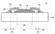
- FIG. 1 is a cross-sectional view showing a configuration of a light emitting device 10 according to an embodiment.
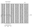
- the supervisor P looks at the light emission surface of the light emitting device 10 from a direction perpendicular to the substrate 100 in FIG.
- FIG. 2 is an enlarged view of the light emitting unit 140 of the light emitting device 10.
- the light emitting device 10 according to the embodiment is a lighting device or a display device. 1 and 2 show a case where the light emitting device 10 is a lighting device.
- the light emitting device 10 includes a substrate 100, a plurality of light emitting units 140, and an insulating film 150.
- the substrate 100 is made of a light transmissive material.
- the plurality of light emitting units 140 are separated from each other, and all include the first electrode 110, the organic layer 120, and the second electrode 130.
- the first electrode 110 is a light-transmitting electrode
- the second electrode 130 is a light-shielding electrode, and at least partly overlaps the first electrode 110.
- the second electrode 130 may be a translucent electrode.
- the organic layer 120 is located between the first electrode 110 and the second electrode 130.
- the insulating film 150 covers the edge of the first electrode 110. Further, at least a part of the insulating film 150 is not covered with the second electrode 130.
- the light emitting device 10 When viewed from a direction perpendicular to the substrate 100, the light emitting device 10 includes a first region 102, a second region 104, and a third region 106.
- the first region 102 is a region overlapping with the second electrode 130. That is, the first region 102 is a region covered with the second electrode 130 when viewed from a direction perpendicular to the substrate 100.
- the second electrode 130 has a light shielding property
- the first region 102 is a region that does not transmit light.
- the second region 104 is a region including the insulating film 150 among regions between the plurality of light emitting units 140.
- the third region 106 is a region that does not include the insulating film 150 among regions between the plurality of light emitting units 140.
- the width of the second region 104 is narrower than the width of the third region 106. Details will be described below.
- the substrate 100 is a light-transmitting substrate such as a glass substrate or a resin substrate.
- the substrate 100 may have flexibility. In the case of flexibility, the thickness of the substrate 100 is, for example, 10 ⁇ m or more and 1000 ⁇ m or less.
- the substrate 100 is, for example, a polygon such as a rectangle or a circle.
- the substrate 100 is formed using, for example, PEN (polyethylene naphthalate), PES (polyethersulfone), PET (polyethylene terephthalate), or polyimide.
- an inorganic barrier film such as SiN x or SiON is formed on at least one surface (preferably both surfaces) of the substrate 100 in order to prevent moisture from permeating the substrate 100. It is preferable.
- a light emitting unit 140 is formed on one surface of the substrate 100.
- the light emitting unit 140 has a configuration in which the first electrode 110, the organic layer 120, and the second electrode 130 are stacked in this order.
- the plurality of light emitting units 140 extend in a line shape.
- the plurality of light emitting units 140 are arranged so as to form a matrix, or form a segment or display a predetermined shape (for example, display an icon). It may be.
- the plurality of light emitting units 140 are formed for each pixel.
- the first electrode 110 is a transparent electrode having optical transparency.
- the material of the transparent electrode is a metal-containing material, for example, a metal oxide such as ITO (Indium Tin Oxide), IZO (Indium Zinc Oxide), IWZO (Indium Tungsten Zinc Oxide), or ZnO (Zinc Oxide).
- the thickness of the first electrode 110 is, for example, not less than 10 nm and not more than 500 nm.
- the first electrode 110 is formed using, for example, a sputtering method or a vapor deposition method.
- the first electrode 110 may be a carbon nanotube or a conductive organic material such as PEDOT / PSS. In the drawing, a plurality of linear first electrodes 110 are formed on a substrate 100 in parallel with each other. For this reason, the first electrode 110 is not located in the second region 104 and the third region 106.
- the organic layer 120 has a light emitting layer.
- the organic layer 120 has a configuration in which, for example, a hole injection layer, a light emitting layer, and an electron injection layer are stacked in this order.
- a hole transport layer may be formed between the hole injection layer and the light emitting layer.
- an electron transport layer may be formed between the light emitting layer and the electron injection layer.
- the organic layer 120 may be formed by a vapor deposition method.
- at least one layer of the organic layer 120, for example, a layer in contact with the first electrode 110, may be formed by a coating method such as an inkjet method, a printing method, or a spray method. In this case, the remaining layers of the organic layer 120 are formed by vapor deposition.
- all the layers of the organic layer 120 may be formed using the apply
- the second electrode 130 is made of, for example, a metal selected from the first group consisting of Al, Au, Ag, Pt, Mg, Sn, Zn, and In, or an alloy of a metal selected from the first group. Contains a metal layer. In this case, the second electrode 130 has a light shielding property.
- the thickness of the second electrode 130 is, for example, not less than 10 nm and not more than 500 nm. However, the second electrode 130 may be formed using the material exemplified as the material of the first electrode 110.
- the second electrode 130 is formed using, for example, a sputtering method or a vapor deposition method. In the example shown in this drawing, the light emitting device 10 has a plurality of linear second electrodes 130.
- the second electrode 130 is provided for each of the first electrodes 110 and is wider than the first electrode 110. For this reason, when viewed from the direction perpendicular to the substrate 100, the entire first electrode 110 is overlapped and covered by the second electrode 130 in the width direction. Further, the first electrode 110 is wider than the second electrode 130, and when viewed from a direction perpendicular to the substrate 100, the first electrode 110 may be entirely covered with the first electrode 110 in the width direction. Good.
- the edge of the first electrode 110 is covered with an insulating film 150.
- the insulating film 150 is made of, for example, a photosensitive resin material such as polyimide, and surrounds a portion of the first electrode 110 that becomes the light emitting portion 140.
- An edge in the width direction of the second electrode 130 is located on the insulating film 150. In other words, when viewed from a direction perpendicular to the substrate 100, a part of the insulating film 150 protrudes from the second electrode 130.
- the organic layer 120 is also formed on the top and side surfaces of the insulating film 150. However, the organic layer 120 is divided between the adjacent light emitting units 140.
- the light emitting device 10 includes the first region 102, the second region 104, and the third region 106.
- the first region 102 is a region overlapping with the second electrode 130.
- the second region 104 is a region including the insulating film 150 among regions between the plurality of light emitting units 140.
- the organic layer 120 is also formed in the second region 104.
- the third region 106 is a region that does not include the insulating film 150 among regions between the plurality of light emitting units 140.
- the organic layer 120 is not formed in at least a part of the third region 106.
- the width of the second region 104 is narrower than the width of the third region 106.
- the width of the third region 106 may be wider or narrower than that of the first region 102.
- the width of the second region 104 is, for example, 0 or more (or more than 0) 0.2 or less
- the width of the third region 106 is, for example, 0.3 or more and 2 or less.
- the width of the first region 102 is, for example, 50 ⁇ m or more and 500 ⁇ m or less
- the width of the second region 104 is, for example, 0 ⁇ m or more (or more than 0 ⁇ m)
- the width of the third region 106 is, for example, 15 ⁇ m or more and 1000 ⁇ m or less. is there.
- FIG. 3 is a plan view of the light emitting device 10. 1 corresponds to the AA cross section of FIG.
- the first region 102, the second region 104, and the third region 106 are all linear and extend in the same direction.
- the second area 104, the first area 102, the second area 104, and the third area 106 are repeatedly arranged in this order.
- the first electrode 110 is formed on the substrate 100 by using, for example, a sputtering method.
- the first electrode 110 is formed into a predetermined pattern using, for example, a photolithography method.
- the insulating film 150 is formed on the edge of the first electrode 110.
- the organic layer 120 and the second electrode 130 are formed in this order.
- the organic layer 120 includes a layer formed by an evaporation method, this layer is formed in a predetermined pattern using, for example, a mask.
- the second electrode 130 is also formed in a predetermined pattern using, for example, a mask.
- the light emitting unit 140 is sealed using a sealing member (not shown).
- the first region 102 has the lowest light transmittance.
- the second region 104 has a lower light transmittance than the third region 106 due to the presence of the insulating film 150.
- the width of the second region 104 is narrower than the width of the third region 106. For this reason, in the light emitting device 10, the area occupancy of the second region 104 is lower than the area occupancy of the third region 106. Therefore, the light transmittance of the light emitting device 10 is increased.
- the insulating film 150 is formed of a light transmissive material, generally, the light transmittance of the light transmissive material varies depending on the wavelength of light. For this reason, when the width of the insulating film 150 is wide, the spectral distribution of the light changes when light passes through the insulating film 150. In this case, when an object is viewed through the light emitting device 10, the color of the object looks different from the actual color. That is, the color of the object changes through the light emitting device 10. For example, when the absorption at a blue wavelength of 400 nm to 600 nm is 50% and is larger than the absorption at other wavelengths, the blue color becomes weak and yellowish when viewed through the light emitting device 10. In contrast, in the present embodiment, since the width of the second region 104 is narrower than the width of the third region 106, the above-described color change can be suppressed.
- FIG. 4 is a cross-sectional view illustrating a configuration of the light emitting device 10 according to Example 1, and corresponds to FIG. 1 in the embodiment.
- the light emitting device 10 according to the present example has the same configuration as the light emitting device 10 according to the embodiment except for the layout of the organic layer 120.
- the organic layer 120 is formed on the entire surface of the third region 106. In other words, the organic layer 120 is continuously formed over the first region 102, the second region 104, and the third region 106. The organic layer 120 is continuously formed so as to connect the plurality of light emitting units 140.
- the light transmittance of the light emitting device 10 is increased as in the embodiment. Moreover, since the organic layer 120 is formed continuously, the cost for forming the organic layer 120 is reduced.
- FIG. 5 is a cross-sectional view illustrating a configuration of the light emitting device 10 according to Example 2, and corresponds to FIG. 2 in the embodiment.
- the light emitting device 10 according to the present example has the same configuration as the light emitting device 10 according to Example 1 except for the width of the second electrode 130.
- the width of the second electrode 130 is narrower than the width of the first electrode 110. For this reason, when viewed from a direction perpendicular to the substrate 100, the end portion of the first electrode 110 in the width direction protrudes from the second electrode 130. In other words, a part of the second region 104 overlaps the first electrode 110.
- the light transmittance of the light emitting device 10 is increased as in the embodiment.
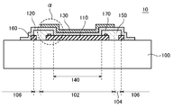
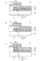
- FIG. 6 is a cross-sectional view illustrating a configuration of the light emitting device 10 according to Example 3, and corresponds to FIG. 2 in the embodiment.
- the light emitting device 10 according to the present example has the same configuration as that of the light emitting device 10 according to Example 1, except that the peeling preventing unit 160 is provided.
- the peeling preventing unit 160 is provided on the surface of the substrate 100 where the light emitting unit 140 is formed.
- the peeling prevention unit 160 is insulated from the first electrode 110 and is formed of a material having higher adhesion to the insulating film 150 than the substrate 100.
- the insulating film 150 is formed from the edge of the first electrode 110 to the peeling prevention unit 160.
- the peeling prevention unit 160 is made of the same material as the first electrode 110 and is physically separated from the first electrode 110 to be insulated from the first electrode 110. ing. In this case, the peeling prevention unit 160 is formed in the same process as the first electrode 110.
- the insulating film 150 is also formed on a region of the substrate 100 located between the peeling prevention unit 160 and the first electrode 110. The edge of the insulating film 150 is located on the peeling prevention unit 160.
- the light transmittance of the light emitting device 10 is increased as in the embodiment. Further, the edge of the insulating film 150 is located on the peeling preventing portion 160.
- the peeling prevention unit 160 has higher adhesion to the insulating film 150 than the substrate 100. Accordingly, the insulating film 150 can be prevented from peeling off.
- FIG. 7 is a cross-sectional view illustrating a configuration of the light emitting device 10 according to Example 4, and corresponds to FIG. 2 in the embodiment.
- the light emitting device 10 according to the present example has the same configuration as that of the light emitting device 10 according to Example 3, except that the conductive portion 170 is provided.
- the conductive part 170 is, for example, an auxiliary electrode of the first electrode 110 and is in contact with the first electrode 110.
- the conductive portion 170 is formed of a material having a lower resistance value than that of the first electrode 110, and is formed using, for example, at least one metal layer.
- the conductive portion 170 has a configuration in which, for example, a first metal layer such as Mo or Mo alloy, a second metal layer such as Al or Al alloy, and a third metal layer such as Mo or Mo alloy are stacked in this order. Yes. Of these three metal layers, the second metal layer is the thickest.
- the conductive portion 170 is covered with the insulating film 150. For this reason, the conductive part 170 is not directly connected to either the organic layer 120 or the second electrode 130.
- FIG. 8A is a first example of an enlarged view of a region surrounded by a dotted line ⁇ in FIG.
- the conductive portion 170 has a configuration in which a second layer 174 is stacked on a first layer 172.
- the first layer 172 is formed of a metal such as Al or an Al alloy, for example, and the second layer 174 is formed of a conductive material having a higher hardness and a lower etching rate than the first layer 172, for example, Mo or an Mo alloy.
- the first layer 172 is made of a material having a lower resistance than the second layer 174.
- the second layer 174 is formed of a MoNb alloy.
- the thickness of the first layer 172 is, for example, not less than 50 nm and not more than 1000 nm. Preferably it is 600 nm or less.
- the second layer 174 is thinner than the first layer 172.
- the thickness of the second layer 174 is, for example, 100 nm or less, preferably 60 nm or less, more preferably 30 nm or less.
- the visible light reflectance of the second layer 174 is lower than the visible light reflectance of the first layer 172.
- the reflectance of the second layer 174 is about 60%
- the reflectance of the first layer 172 is about 90%.
- the width of the first layer 172 is narrower than the width of the second layer 174. For this reason, in the width direction of the conductive portion 170, the end portion of the first layer 172 is located closer to the center of the conductive portion 170 than the end portion of the second layer 174.
- the distance d between the end of the first layer 172 and the end of the second layer 174 is preferably 150 nm or more, more preferably 300 nm or more.
- the conductive part 170 overlaps the second electrode 130.
- the width w of the conductive portion 170 overlapping the second electrode 130 is preferably, for example, 150 nm or more. In the example shown in this drawing, the entire conductive portion 170 overlaps the second electrode 130.
- the timing for forming the conductive portion 170 is after the first electrode 110 is formed and before the insulating film 150 is formed.
- the conductive portion 170 is formed as follows, for example. First, the first layer 172 and the second layer 174 are formed in this order by using a film forming method such as a sputtering method. Next, a resist pattern (not shown) is formed on the second layer 174, and the second layer 174 and the first layer 172 are etched (for example, wet etching) using the resist pattern as a mask. At this time, the etching is made isotropic. Also, under this etching condition, the etching rate of the first layer 172 is faster than the etching rate of the second layer 174.
- the first layer 172 is etched faster than the second layer 174.
- the side surface of the first layer 172 enters the center side of the conductive portion 170 more than the side surface of the second layer 174. That is, the end portion of the first layer 172 is located closer to the center of the conductive portion 170 than the end portion of the second layer 174.
- the size of the interval d is controlled by adjusting etching conditions (for example, etching time).
- the light transmittance of the light emitting device 10 is increased as in the embodiment. Further, since the conductive portion 170 is formed on the first electrode 110, the apparent resistance value of the first electrode 110 can be lowered. Moreover, it is suppressed that the color of the thing when seeing an object via the light-emitting device 10 looks different from an actual color.
- the conductive portion 170 is covered with the insulating film 150, when light is reflected from the end face of the conductive portion 170, the amount of light transmitted through the insulating film 150 increases. Since the light transmittance of the insulating film 150 varies depending on the wavelength of light, when the amount of light transmitted through the insulating film 150 increases, the color of the object changes when the object is viewed through the light emitting device 10. The chance of seeing is increased.
- the visible light reflectance of the second layer 174 is lower than the visible light reflectance of the first layer 172. The end portion of the first layer 172 is located closer to the center of the conductive portion 170 than the end portion of the second layer 174. Accordingly, at least part of the light incident on the end portion of the first layer 172 is blocked by the second layer 174. Thereby, the amount of light transmitted through the insulating film 150 can be reduced.
- the conductive portion 170 may have a configuration in which the first layer 172 is stacked on the second layer 174. In this case, at least a part of the light reflected by the end portion of the first layer 172 is blocked by the second layer 174 before entering the substrate 100. Thereby, the amount of light transmitted through the insulating film 150 can be reduced.
- the conductive portion 170 may have a configuration in which the second layer 174, the first layer 172, and the second layer 174 are stacked in this order.
- the film thicknesses of the two second layers 174 may be different from each other or the same.
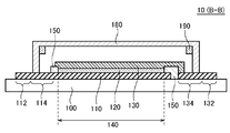
- FIG. 9 is a cross-sectional view illustrating a configuration of the light emitting device 10 according to the fifth embodiment.
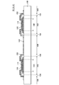
- FIG. 10 is a plan view of the light emitting device 10 shown in FIG. However, some members are omitted in FIG. FIG. 9 corresponds to the BB cross section of FIG.
- the light emitting device 10 according to this example has the same configuration as that of the light emitting device 10 according to the embodiment or any of Examples 1 to 4 except that the sealing member 180 and the desiccant 190 are provided.
- the planar shape of the substrate 100 is, for example, a polygon such as a rectangle or a circle.
- the sealing member 180 has translucency and is formed using, for example, glass or resin.
- the sealing member 180 is a polygon or a circle similar to the substrate 100, and has a shape in which a recess is provided at the center.
- the edge of the sealing member 180 is fixed to the substrate 100 with an adhesive. Thereby, the space surrounded by the sealing member 180 and the substrate 100 is sealed.
- the plurality of light emitting units 140 are all located in a sealed space.
- the light emitting device 10 includes a first terminal 112, a first lead wire 114, a second terminal 132, and a second lead wire 134.
- the first terminal 112, the first lead wiring 114, the second terminal 132, and the second lead wiring 134 are all formed on the same surface of the substrate 100 as the light emitting unit 140.
- the first terminal 112 and the second terminal 132 are located outside the sealing member 180.
- the first lead wire 114 connects the first terminal 112 and the first electrode 110
- the second lead wire 134 connects the second terminal 132 and the second electrode 130.
- each of the first lead wiring 114 and the second lead wiring 134 extends from the inside to the outside of the sealing member 180.
- the first terminal 112, the second terminal 132, the first lead wiring 114, and the second lead wiring 134 have, for example, a layer formed of the same material as that of the first electrode 110.
- at least a part of at least one of the first terminal 112, the second terminal 132, the first lead wiring 114, and the second lead wiring 134 is a metal film having a lower resistance than the first electrode 110 on this layer. (For example, a film similar to the conductive portion 170) may be included. This metal film does not need to be formed on all of the first terminal 112, the second terminal 132, the first lead wiring 114, and the second lead wiring 134.
- the first terminal 112 the first lead wire 114, the second terminal 132, and the second lead wire 134
- a layer formed of the same material as the first electrode 110 is formed in the same process as the first electrode 110. Yes.
- the first electrode 110 is integrated with at least a part of the layer of the first terminal 112.
- the metal film is formed in the same process as that of the conductive portion 170, for example.
- the light transmittance of the first terminal 112, the first lead wire 114, the second terminal 132, and the second lead wire 134 is lower than the light transmittance of the substrate 100.
- the first lead-out wiring 114 and the second lead-out wiring 134 are formed one by one for one light emitting unit 140.
- the plurality of first lead wires 114 are all connected to the same first terminal 112, and the plurality of second lead wires 134 are all connected to the same second terminal 132.
- the first terminal 112 is connected to a positive terminal of a control circuit via a conductive member such as a bonding wire or a lead terminal, and the second terminal 132 is controlled via a conductive member such as a bonding wire or a lead terminal.
- the negative terminal of the circuit is connected.
- the desiccant 190 is a region sealed with the sealing member 180 and does not overlap any of the light emitting portions 140 when viewed from a direction perpendicular to the substrate 100, for example, the first extraction wiring 114 and the first wiring. It is arranged in a region overlapping with at least one of the two lead wires 134.
- the desiccant 190 contains a drying member such as CaO or BaO.
- the light transmittance of the desiccant 190 is lower than the light transmittance of the substrate 100.
- the desiccant 190 is fixed to the surface of the sealing member 180 that faces the substrate 100.
- the desiccant 190 is disposed in each of the region overlapping the first lead wiring 114 and the region overlapping the second lead wiring 134.
- the desiccant 190 is disposed along two opposite sides of the rectangular substrate 100, but is disposed along the remaining two sides, that is, the remaining two sides and the light emitting unit 140. Not.
- FIG. 11 is a plan view showing a modification of FIG.
- a part of the first terminal 112 and the second terminal 132 is located inside the sealing member 180.
- At least a part of the desiccant 190 overlaps at least one of the first terminal 112 and the second terminal 132.
- the light transmittance of the light emitting device 10 is increased as in the embodiment. Further, when viewed from a direction perpendicular to the substrate 100, the desiccant 190 does not overlap the light emitting unit 140 and is located near the edge of the substrate 100. Therefore, as compared with the case where the desiccant 190 is provided at a position overlapping the light emitting unit 140, the desiccant 190 is less visible to the user. In particular, in the present embodiment, the desiccant 190 overlaps the first lead wiring 114 and the second lead wiring 134. The first lead wiring 114 and the second lead wiring 134 also have low light transmittance.
- the light transmittance of the light-emitting device 10 improves.
- the first terminal 112 and the second terminal 132 are overlapped with the desiccant 190, the light transmittance of the light emitting device 10 is greatly improved as compared with the case where they are not overlapped.
- the luminance of the light emitting unit 140 varies depending on the temperature of the organic layer 120.
- the desiccant 190 is provided at a position overlapping the organic layer 120, at least a part of the heat radiated from the light emitting unit 140 is absorbed by the desiccant 190. Therefore, the temperature of the region of the organic layer 120 that overlaps with the desiccant 190 is lower than the other regions of the organic layer 120. In this case, in-plane variation occurs in the luminance of the light emitting unit 140.
- the desiccant 190 does not overlap the light emitting unit 140. Therefore, it is possible to suppress in-plane variation in the luminance of the light emitting unit 140.
- the desiccant 190 is provided at a position overlapping the first extraction wiring 114 and a position overlapping the second extraction wiring 134. Accordingly, the temperature of the region located near the first lead wire 114 in the organic layer 120 and the temperature of the region located near the second lead wire 134 are both the center of the light emitting unit 140 in the organic layer 120. It becomes lower than the temperature of the region located in the part. Thereby, the variation in the luminance of the light emitting unit 140 due to the resistance of the first electrode 110 and the second electrode 130 is absorbed. Accordingly, the in-plane variation in luminance of the light emitting unit 140 is reduced.
Landscapes
- Physics & Mathematics (AREA)
- Optics & Photonics (AREA)
- Engineering & Computer Science (AREA)
- Microelectronics & Electronic Packaging (AREA)
- Geometry (AREA)
- Manufacturing & Machinery (AREA)
- Electroluminescent Light Sources (AREA)
Abstract
Priority Applications (5)
| Application Number | Priority Date | Filing Date | Title |
|---|---|---|---|
| EP14901900.2A EP3197244A4 (fr) | 2014-09-18 | 2014-09-18 | Dispositif électroluminescent |
| PCT/JP2014/074692 WO2016042638A1 (fr) | 2014-09-18 | 2014-09-18 | Dispositif électroluminescent |
| US15/512,829 US20170294626A1 (en) | 2014-09-18 | 2014-09-18 | Light-emitting device |
| KR1020177009952A KR20170057336A (ko) | 2014-09-18 | 2014-09-18 | 발광 장치 |
| JP2016548492A JPWO2016042638A1 (ja) | 2014-09-18 | 2014-09-18 | 発光装置 |
Applications Claiming Priority (1)
| Application Number | Priority Date | Filing Date | Title |
|---|---|---|---|
| PCT/JP2014/074692 WO2016042638A1 (fr) | 2014-09-18 | 2014-09-18 | Dispositif électroluminescent |
Publications (1)
| Publication Number | Publication Date |
|---|---|
| WO2016042638A1 true WO2016042638A1 (fr) | 2016-03-24 |
Family
ID=55532704
Family Applications (1)
| Application Number | Title | Priority Date | Filing Date |
|---|---|---|---|
| PCT/JP2014/074692 WO2016042638A1 (fr) | 2014-09-18 | 2014-09-18 | Dispositif électroluminescent |
Country Status (5)
| Country | Link |
|---|---|
| US (1) | US20170294626A1 (fr) |
| EP (1) | EP3197244A4 (fr) |
| JP (1) | JPWO2016042638A1 (fr) |
| KR (1) | KR20170057336A (fr) |
| WO (1) | WO2016042638A1 (fr) |
Cited By (9)
| Publication number | Priority date | Publication date | Assignee | Title |
|---|---|---|---|---|
| WO2017149771A1 (fr) * | 2016-03-04 | 2017-09-08 | パイオニア株式会社 | Dispositif d'émission de lumière et procédé d'émission de lumière |
| WO2017183118A1 (fr) * | 2016-04-19 | 2017-10-26 | パイオニア株式会社 | Dispositif électroluminescent |
| JP2018010780A (ja) * | 2016-07-13 | 2018-01-18 | パイオニア株式会社 | 発光装置 |
| WO2018061102A1 (fr) * | 2016-09-28 | 2018-04-05 | パイオニア株式会社 | Dispositif électroluminescent |
| JP2018073526A (ja) * | 2016-10-26 | 2018-05-10 | パイオニア株式会社 | 発光装置 |
| WO2018116894A1 (fr) * | 2016-12-19 | 2018-06-28 | パイオニア株式会社 | Dispositif d'émission de lumière et procédé d'émission de lumière |
| JP2020064851A (ja) * | 2019-09-25 | 2020-04-23 | パイオニア株式会社 | 発光装置 |
| JP2022016557A (ja) * | 2017-02-27 | 2022-01-21 | パイオニア株式会社 | 発光装置 |
| JP2022522493A (ja) * | 2019-06-28 | 2022-04-19 | 昆山国顕光電有限公司 | ディスプレイ基板、ディスプレイパネル、及びディスプレイ装置 |
Families Citing this family (1)
| Publication number | Priority date | Publication date | Assignee | Title |
|---|---|---|---|---|
| CN110071158B (zh) * | 2019-04-29 | 2021-08-31 | 上海天马有机发光显示技术有限公司 | 一种掩膜版和有机发光显示面板 |
Citations (12)
| Publication number | Priority date | Publication date | Assignee | Title |
|---|---|---|---|---|
| JPH03250583A (ja) * | 1990-02-28 | 1991-11-08 | Idemitsu Kosan Co Ltd | エレクトロルミネッセンス素子及びその製造方法 |
| JP2000075836A (ja) * | 1998-09-02 | 2000-03-14 | Sharp Corp | 有機el発光装置とその駆動方法 |
| JP2000252063A (ja) * | 1999-03-01 | 2000-09-14 | Toppan Printing Co Ltd | 色切換発光素子、色切換発光素子用基板及びカラー表示装置 |
| JP2000252062A (ja) * | 1999-03-04 | 2000-09-14 | Pioneer Electronic Corp | 発光ディスプレイパネルの製造方法 |
| JP2001338770A (ja) * | 2000-05-26 | 2001-12-07 | Tohoku Pioneer Corp | 発光表示装置及びその製造方法 |
| JP2004119226A (ja) * | 2002-09-27 | 2004-04-15 | Nippon Seiki Co Ltd | 有機elパネル |
| JP2004527088A (ja) * | 2001-04-26 | 2004-09-02 | コーニンクレッカ フィリップス エレクトロニクス エヌ ヴィ | エレクトロルミネセント装置及びその製造方法 |
| JP2004327215A (ja) * | 2003-04-24 | 2004-11-18 | Seiko Epson Corp | 電気光学装置、電気光学装置用基板、電気光学装置の製造方法および電子機器 |
| JP2007258688A (ja) * | 2006-02-24 | 2007-10-04 | Sumitomo Chemical Co Ltd | 発光装置 |
| JP2008004290A (ja) * | 2006-06-20 | 2008-01-10 | Nippon Hoso Kyokai <Nhk> | 有機el表示装置および有機el表示装置の製造方法 |
| JP2010504608A (ja) * | 2006-09-22 | 2010-02-12 | ケンブリッジ ディスプレイ テクノロジー リミテッド | 分子電子素子の製造方法及び構造体 |
| WO2014069316A1 (fr) * | 2012-10-31 | 2014-05-08 | シャープ株式会社 | Substrat électroluminescent, son procédé de production, panneau d'affichage électroluminescent et dispositif d'affichage électroluminescent |
Family Cites Families (11)
| Publication number | Priority date | Publication date | Assignee | Title |
|---|---|---|---|---|
| JP4399839B2 (ja) * | 2007-02-01 | 2010-01-20 | エプソンイメージングデバイス株式会社 | 表示装置 |
| US9721998B2 (en) * | 2011-11-04 | 2017-08-01 | Semiconductor Energy Laboratory Co., Ltd. | Display device and driving method thereof |
| KR101932564B1 (ko) * | 2011-11-29 | 2018-12-28 | 삼성디스플레이 주식회사 | 유기 발광 표시 장치 |
| JP5970811B2 (ja) * | 2011-12-28 | 2016-08-17 | セイコーエプソン株式会社 | 発光素子、発光装置および電子機器 |
| JP6225413B2 (ja) * | 2012-11-16 | 2017-11-08 | セイコーエプソン株式会社 | 機能層形成用インク、インク容器、吐出装置、機能層の形成方法、有機el素子の製造方法 |
| JP2014154566A (ja) * | 2013-02-04 | 2014-08-25 | Toshiba Corp | 有機電界発光素子、照明装置及び照明システム |
| JP6157866B2 (ja) * | 2013-02-04 | 2017-07-05 | 株式会社東芝 | 有機電界発光素子、照明装置及び照明システム |
| JP5584329B1 (ja) * | 2013-02-04 | 2014-09-03 | 株式会社東芝 | 有機電界発光素子、照明装置及び照明システム |
| KR102139577B1 (ko) * | 2013-10-24 | 2020-07-31 | 삼성디스플레이 주식회사 | 유기 발광 표시 장치 |
| JP6535977B2 (ja) * | 2014-03-27 | 2019-07-03 | セイコーエプソン株式会社 | 発光素子の製造方法 |
| US9478763B2 (en) * | 2014-04-04 | 2016-10-25 | Seiko Epson Corporation | Light emitting element, light emitting device, display apparatus, and electronic equipment having a light emitting layer with host and assist dopant materials with different electron and hole transportation properties |
-
2014
- 2014-09-18 US US15/512,829 patent/US20170294626A1/en not_active Abandoned
- 2014-09-18 EP EP14901900.2A patent/EP3197244A4/fr not_active Withdrawn
- 2014-09-18 JP JP2016548492A patent/JPWO2016042638A1/ja active Pending
- 2014-09-18 KR KR1020177009952A patent/KR20170057336A/ko active Search and Examination
- 2014-09-18 WO PCT/JP2014/074692 patent/WO2016042638A1/fr active Application Filing
Patent Citations (12)
| Publication number | Priority date | Publication date | Assignee | Title |
|---|---|---|---|---|
| JPH03250583A (ja) * | 1990-02-28 | 1991-11-08 | Idemitsu Kosan Co Ltd | エレクトロルミネッセンス素子及びその製造方法 |
| JP2000075836A (ja) * | 1998-09-02 | 2000-03-14 | Sharp Corp | 有機el発光装置とその駆動方法 |
| JP2000252063A (ja) * | 1999-03-01 | 2000-09-14 | Toppan Printing Co Ltd | 色切換発光素子、色切換発光素子用基板及びカラー表示装置 |
| JP2000252062A (ja) * | 1999-03-04 | 2000-09-14 | Pioneer Electronic Corp | 発光ディスプレイパネルの製造方法 |
| JP2001338770A (ja) * | 2000-05-26 | 2001-12-07 | Tohoku Pioneer Corp | 発光表示装置及びその製造方法 |
| JP2004527088A (ja) * | 2001-04-26 | 2004-09-02 | コーニンクレッカ フィリップス エレクトロニクス エヌ ヴィ | エレクトロルミネセント装置及びその製造方法 |
| JP2004119226A (ja) * | 2002-09-27 | 2004-04-15 | Nippon Seiki Co Ltd | 有機elパネル |
| JP2004327215A (ja) * | 2003-04-24 | 2004-11-18 | Seiko Epson Corp | 電気光学装置、電気光学装置用基板、電気光学装置の製造方法および電子機器 |
| JP2007258688A (ja) * | 2006-02-24 | 2007-10-04 | Sumitomo Chemical Co Ltd | 発光装置 |
| JP2008004290A (ja) * | 2006-06-20 | 2008-01-10 | Nippon Hoso Kyokai <Nhk> | 有機el表示装置および有機el表示装置の製造方法 |
| JP2010504608A (ja) * | 2006-09-22 | 2010-02-12 | ケンブリッジ ディスプレイ テクノロジー リミテッド | 分子電子素子の製造方法及び構造体 |
| WO2014069316A1 (fr) * | 2012-10-31 | 2014-05-08 | シャープ株式会社 | Substrat électroluminescent, son procédé de production, panneau d'affichage électroluminescent et dispositif d'affichage électroluminescent |
Non-Patent Citations (1)
| Title |
|---|
| See also references of EP3197244A4 * |
Cited By (18)
| Publication number | Priority date | Publication date | Assignee | Title |
|---|---|---|---|---|
| US10991908B2 (en) | 2016-03-04 | 2021-04-27 | Pioneer Corporation | Light-emitting device and light-emitting system |
| US11706947B2 (en) | 2016-03-04 | 2023-07-18 | Pioneer Corporation | Light-emitting device and light-emitting system |
| JPWO2017149771A1 (ja) * | 2016-03-04 | 2018-12-27 | パイオニア株式会社 | 発光装置および発光システム |
| WO2017149771A1 (fr) * | 2016-03-04 | 2017-09-08 | パイオニア株式会社 | Dispositif d'émission de lumière et procédé d'émission de lumière |
| WO2017183118A1 (fr) * | 2016-04-19 | 2017-10-26 | パイオニア株式会社 | Dispositif électroluminescent |
| JP2018010780A (ja) * | 2016-07-13 | 2018-01-18 | パイオニア株式会社 | 発光装置 |
| WO2018061102A1 (fr) * | 2016-09-28 | 2018-04-05 | パイオニア株式会社 | Dispositif électroluminescent |
| JPWO2018061102A1 (ja) * | 2016-09-28 | 2019-07-11 | パイオニア株式会社 | 発光装置 |
| JP2018073526A (ja) * | 2016-10-26 | 2018-05-10 | パイオニア株式会社 | 発光装置 |
| JPWO2018116894A1 (ja) * | 2016-12-19 | 2019-10-24 | パイオニア株式会社 | 発光装置及び発光システム |
| US20200091466A1 (en) * | 2016-12-19 | 2020-03-19 | Pioneer Corporation | Light-emitting device and light-emitting system |
| US11335890B2 (en) | 2016-12-19 | 2022-05-17 | Pioneer Corporation | Light-emitting device and light-emitting system |
| WO2018116894A1 (fr) * | 2016-12-19 | 2018-06-28 | パイオニア株式会社 | Dispositif d'émission de lumière et procédé d'émission de lumière |
| JP2022016557A (ja) * | 2017-02-27 | 2022-01-21 | パイオニア株式会社 | 発光装置 |
| JP2022522493A (ja) * | 2019-06-28 | 2022-04-19 | 昆山国顕光電有限公司 | ディスプレイ基板、ディスプレイパネル、及びディスプレイ装置 |
| JP7213367B2 (ja) | 2019-06-28 | 2023-01-26 | 昆山国顕光電有限公司 | ディスプレイ基板、ディスプレイパネル、及びディスプレイ装置 |
| JP2020064851A (ja) * | 2019-09-25 | 2020-04-23 | パイオニア株式会社 | 発光装置 |
| JP2021128945A (ja) * | 2019-09-25 | 2021-09-02 | パイオニア株式会社 | 発光装置 |
Also Published As
| Publication number | Publication date |
|---|---|
| JPWO2016042638A1 (ja) | 2017-06-15 |
| KR20170057336A (ko) | 2017-05-24 |
| US20170294626A1 (en) | 2017-10-12 |
| EP3197244A1 (fr) | 2017-07-26 |
| EP3197244A4 (fr) | 2018-06-06 |
Similar Documents
| Publication | Publication Date | Title |
|---|---|---|
| WO2016042638A1 (fr) | Dispositif électroluminescent | |
| JP6807178B2 (ja) | 表示装置、表示装置の製造方法 | |
| JP2016062767A (ja) | 発光装置 | |
| WO2018061102A1 (fr) | Dispositif électroluminescent | |
| WO2017138633A1 (fr) | Dispositif électroluminescent | |
| WO2017073459A1 (fr) | Système électroluminescent | |
| JP6522311B2 (ja) | 発光装置 | |
| JP2016062766A (ja) | 発光装置 | |
| WO2016151820A1 (fr) | Dispositif électroluminescent | |
| JP6457065B2 (ja) | 発光装置 | |
| WO2018163937A1 (fr) | Dispositif électroluminescent | |
| JP2016072283A (ja) | 発光装置 | |
| JP2018037202A (ja) | 発光装置 | |
| JP6450124B2 (ja) | 発光装置 | |
| WO2017094498A1 (fr) | Système électroluminescent | |
| JP2019036758A (ja) | 発光装置 | |
| JP2017216203A (ja) | 発光装置 | |
| WO2018151026A1 (fr) | Dispositif électroluminescent | |
| WO2017094499A1 (fr) | Dispositif électroluminescent | |
| WO2017183118A1 (fr) | Dispositif électroluminescent | |
| JP2024023850A (ja) | 発光装置 | |
| JP2022174312A (ja) | 発光装置 | |
| JP2022173480A (ja) | 発光装置 | |
| WO2018025576A1 (fr) | Dispositif électroluminescent | |
| WO2017187639A1 (fr) | Appareil électroluminescent |
Legal Events
| Date | Code | Title | Description |
|---|---|---|---|
| 121 | Ep: the epo has been informed by wipo that ep was designated in this application |
Ref document number: 14901900 Country of ref document: EP Kind code of ref document: A1 |
|
| ENP | Entry into the national phase |
Ref document number: 2016548492 Country of ref document: JP Kind code of ref document: A |
|
| NENP | Non-entry into the national phase |
Ref country code: DE |
|
| WWE | Wipo information: entry into national phase |
Ref document number: 15512829 Country of ref document: US |
|
| REEP | Request for entry into the european phase |
Ref document number: 2014901900 Country of ref document: EP |
|
| WWE | Wipo information: entry into national phase |
Ref document number: 2014901900 Country of ref document: EP |
|
| ENP | Entry into the national phase |
Ref document number: 20177009952 Country of ref document: KR Kind code of ref document: A |