WO2016038956A1 - 電力変換装置 - Google Patents
電力変換装置 Download PDFInfo
- Publication number
- WO2016038956A1 WO2016038956A1 PCT/JP2015/066428 JP2015066428W WO2016038956A1 WO 2016038956 A1 WO2016038956 A1 WO 2016038956A1 JP 2015066428 W JP2015066428 W JP 2015066428W WO 2016038956 A1 WO2016038956 A1 WO 2016038956A1
- Authority
- WO
- WIPO (PCT)
- Prior art keywords
- power semiconductor
- high thermal
- semiconductor module
- power
- thermal conductor
- Prior art date
- Legal status (The legal status is an assumption and is not a legal conclusion. Google has not performed a legal analysis and makes no representation as to the accuracy of the status listed.)
- Ceased
Links
Images








Classifications
-
- H—ELECTRICITY
- H05—ELECTRIC TECHNIQUES NOT OTHERWISE PROVIDED FOR
- H05K—PRINTED CIRCUITS; CASINGS OR CONSTRUCTIONAL DETAILS OF ELECTRIC APPARATUS; MANUFACTURE OF ASSEMBLAGES OF ELECTRICAL COMPONENTS
- H05K7/00—Constructional details common to different types of electric apparatus
- H05K7/20—Modifications to facilitate cooling, ventilating, or heating
- H05K7/2089—Modifications to facilitate cooling, ventilating, or heating for power electronics, e.g. for inverters for controlling motor
- H05K7/20927—Liquid coolant without phase change
-
- H—ELECTRICITY
- H02—GENERATION; CONVERSION OR DISTRIBUTION OF ELECTRIC POWER
- H02M—APPARATUS FOR CONVERSION BETWEEN AC AND AC, BETWEEN AC AND DC, OR BETWEEN DC AND DC, AND FOR USE WITH MAINS OR SIMILAR POWER SUPPLY SYSTEMS; CONVERSION OF DC OR AC INPUT POWER INTO SURGE OUTPUT POWER; CONTROL OR REGULATION THEREOF
- H02M1/00—Details of apparatus for conversion
- H02M1/08—Circuits specially adapted for the generation of control voltages for semiconductor devices incorporated in static converters
- H02M1/084—Circuits specially adapted for the generation of control voltages for semiconductor devices incorporated in static converters using a control circuit common to several phases of a multi-phase system
-
- H—ELECTRICITY
- H02—GENERATION; CONVERSION OR DISTRIBUTION OF ELECTRIC POWER
- H02M—APPARATUS FOR CONVERSION BETWEEN AC AND AC, BETWEEN AC AND DC, OR BETWEEN DC AND DC, AND FOR USE WITH MAINS OR SIMILAR POWER SUPPLY SYSTEMS; CONVERSION OF DC OR AC INPUT POWER INTO SURGE OUTPUT POWER; CONTROL OR REGULATION THEREOF
- H02M7/00—Conversion of AC power input into DC power output; Conversion of DC power input into AC power output
- H02M7/003—Constructional details, e.g. physical layout, assembly, wiring or busbar connections
-
- H—ELECTRICITY
- H02—GENERATION; CONVERSION OR DISTRIBUTION OF ELECTRIC POWER
- H02M—APPARATUS FOR CONVERSION BETWEEN AC AND AC, BETWEEN AC AND DC, OR BETWEEN DC AND DC, AND FOR USE WITH MAINS OR SIMILAR POWER SUPPLY SYSTEMS; CONVERSION OF DC OR AC INPUT POWER INTO SURGE OUTPUT POWER; CONTROL OR REGULATION THEREOF
- H02M7/00—Conversion of AC power input into DC power output; Conversion of DC power input into AC power output
- H02M7/42—Conversion of DC power input into AC power output without possibility of reversal
- H02M7/44—Conversion of DC power input into AC power output without possibility of reversal by static converters
- H02M7/48—Conversion of DC power input into AC power output without possibility of reversal by static converters using discharge tubes with control electrode or semiconductor devices with control electrode
- H02M7/53—Conversion of DC power input into AC power output without possibility of reversal by static converters using discharge tubes with control electrode or semiconductor devices with control electrode using devices of a triode or transistor type requiring continuous application of a control signal
- H02M7/537—Conversion of DC power input into AC power output without possibility of reversal by static converters using discharge tubes with control electrode or semiconductor devices with control electrode using devices of a triode or transistor type requiring continuous application of a control signal using semiconductor devices only, e.g. single switched pulse inverters
- H02M7/5387—Conversion of DC power input into AC power output without possibility of reversal by static converters using discharge tubes with control electrode or semiconductor devices with control electrode using devices of a triode or transistor type requiring continuous application of a control signal using semiconductor devices only, e.g. single switched pulse inverters in a bridge configuration
-
- H—ELECTRICITY
- H10—SEMICONDUCTOR DEVICES; ELECTRIC SOLID-STATE DEVICES NOT OTHERWISE PROVIDED FOR
- H10W—GENERIC PACKAGES, INTERCONNECTIONS, CONNECTORS OR OTHER CONSTRUCTIONAL DETAILS OF DEVICES COVERED BY CLASS H10
- H10W40/00—Arrangements for thermal protection or thermal control
- H10W40/40—Arrangements for thermal protection or thermal control involving heat exchange by flowing fluids
- H10W40/47—Arrangements for thermal protection or thermal control involving heat exchange by flowing fluids by flowing liquids, e.g. forced water cooling
- H10W40/475—Arrangements for thermal protection or thermal control involving heat exchange by flowing fluids by flowing liquids, e.g. forced water cooling using jet impingement
-
- H—ELECTRICITY
- H10—SEMICONDUCTOR DEVICES; ELECTRIC SOLID-STATE DEVICES NOT OTHERWISE PROVIDED FOR
- H10W—GENERIC PACKAGES, INTERCONNECTIONS, CONNECTORS OR OTHER CONSTRUCTIONAL DETAILS OF DEVICES COVERED BY CLASS H10
- H10W70/00—Package substrates; Interposers; Redistribution layers [RDL]
- H10W70/01—Manufacture or treatment
- H10W70/02—Manufacture or treatment of conductive package substrates serving as an interconnection, e.g. of metal plates
- H10W70/027—Mechanical treatments, e.g. deforming, punching or cutting
-
- H—ELECTRICITY
- H10—SEMICONDUCTOR DEVICES; ELECTRIC SOLID-STATE DEVICES NOT OTHERWISE PROVIDED FOR
- H10W—GENERIC PACKAGES, INTERCONNECTIONS, CONNECTORS OR OTHER CONSTRUCTIONAL DETAILS OF DEVICES COVERED BY CLASS H10
- H10W70/00—Package substrates; Interposers; Redistribution layers [RDL]
- H10W70/40—Leadframes
- H10W70/421—Shapes or dispositions
-
- H—ELECTRICITY
- H10—SEMICONDUCTOR DEVICES; ELECTRIC SOLID-STATE DEVICES NOT OTHERWISE PROVIDED FOR
- H10W—GENERIC PACKAGES, INTERCONNECTIONS, CONNECTORS OR OTHER CONSTRUCTIONAL DETAILS OF DEVICES COVERED BY CLASS H10
- H10W70/00—Package substrates; Interposers; Redistribution layers [RDL]
- H10W70/40—Leadframes
- H10W70/461—Leadframes specially adapted for cooling
-
- H—ELECTRICITY
- H10—SEMICONDUCTOR DEVICES; ELECTRIC SOLID-STATE DEVICES NOT OTHERWISE PROVIDED FOR
- H10W—GENERIC PACKAGES, INTERCONNECTIONS, CONNECTORS OR OTHER CONSTRUCTIONAL DETAILS OF DEVICES COVERED BY CLASS H10
- H10W70/00—Package substrates; Interposers; Redistribution layers [RDL]
- H10W70/40—Leadframes
- H10W70/481—Leadframes for devices being provided for in groups H10D8/00 - H10D48/00
-
- H—ELECTRICITY
- H10—SEMICONDUCTOR DEVICES; ELECTRIC SOLID-STATE DEVICES NOT OTHERWISE PROVIDED FOR
- H10W—GENERIC PACKAGES, INTERCONNECTIONS, CONNECTORS OR OTHER CONSTRUCTIONAL DETAILS OF DEVICES COVERED BY CLASS H10
- H10W74/00—Encapsulations, e.g. protective coatings
- H10W74/01—Manufacture or treatment
-
- H—ELECTRICITY
- H10—SEMICONDUCTOR DEVICES; ELECTRIC SOLID-STATE DEVICES NOT OTHERWISE PROVIDED FOR
- H10W—GENERIC PACKAGES, INTERCONNECTIONS, CONNECTORS OR OTHER CONSTRUCTIONAL DETAILS OF DEVICES COVERED BY CLASS H10
- H10W74/00—Encapsulations, e.g. protective coatings
- H10W74/10—Encapsulations, e.g. protective coatings characterised by their shape or disposition
- H10W74/111—Encapsulations, e.g. protective coatings characterised by their shape or disposition the semiconductor body being completely enclosed
- H10W74/127—Encapsulations, e.g. protective coatings characterised by their shape or disposition the semiconductor body being completely enclosed characterised by arrangements for sealing or adhesion
-
- H—ELECTRICITY
- H10—SEMICONDUCTOR DEVICES; ELECTRIC SOLID-STATE DEVICES NOT OTHERWISE PROVIDED FOR
- H10W—GENERIC PACKAGES, INTERCONNECTIONS, CONNECTORS OR OTHER CONSTRUCTIONAL DETAILS OF DEVICES COVERED BY CLASS H10
- H10W90/00—Package configurations
-
- H—ELECTRICITY
- H10—SEMICONDUCTOR DEVICES; ELECTRIC SOLID-STATE DEVICES NOT OTHERWISE PROVIDED FOR
- H10D—INORGANIC ELECTRIC SEMICONDUCTOR DEVICES
- H10D12/00—Bipolar devices controlled by the field effect, e.g. insulated-gate bipolar transistors [IGBT]
- H10D12/411—Insulated-gate bipolar transistors [IGBT]
-
- H—ELECTRICITY
- H10—SEMICONDUCTOR DEVICES; ELECTRIC SOLID-STATE DEVICES NOT OTHERWISE PROVIDED FOR
- H10W—GENERIC PACKAGES, INTERCONNECTIONS, CONNECTORS OR OTHER CONSTRUCTIONAL DETAILS OF DEVICES COVERED BY CLASS H10
- H10W70/00—Package substrates; Interposers; Redistribution layers [RDL]
- H10W70/40—Leadframes
- H10W70/421—Shapes or dispositions
- H10W70/442—Shapes or dispositions of multiple leadframes in a single chip
-
- H—ELECTRICITY
- H10—SEMICONDUCTOR DEVICES; ELECTRIC SOLID-STATE DEVICES NOT OTHERWISE PROVIDED FOR
- H10W—GENERIC PACKAGES, INTERCONNECTIONS, CONNECTORS OR OTHER CONSTRUCTIONAL DETAILS OF DEVICES COVERED BY CLASS H10
- H10W72/00—Interconnections or connectors in packages
- H10W72/90—Bond pads, in general
- H10W72/921—Structures or relative sizes of bond pads
- H10W72/926—Multiple bond pads having different sizes
-
- H—ELECTRICITY
- H10—SEMICONDUCTOR DEVICES; ELECTRIC SOLID-STATE DEVICES NOT OTHERWISE PROVIDED FOR
- H10W—GENERIC PACKAGES, INTERCONNECTIONS, CONNECTORS OR OTHER CONSTRUCTIONAL DETAILS OF DEVICES COVERED BY CLASS H10
- H10W74/00—Encapsulations, e.g. protective coatings
-
- H—ELECTRICITY
- H10—SEMICONDUCTOR DEVICES; ELECTRIC SOLID-STATE DEVICES NOT OTHERWISE PROVIDED FOR
- H10W—GENERIC PACKAGES, INTERCONNECTIONS, CONNECTORS OR OTHER CONSTRUCTIONAL DETAILS OF DEVICES COVERED BY CLASS H10
- H10W90/00—Package configurations
- H10W90/701—Package configurations characterised by the relative positions of pads or connectors relative to package parts
- H10W90/751—Package configurations characterised by the relative positions of pads or connectors relative to package parts of bond wires
- H10W90/756—Package configurations characterised by the relative positions of pads or connectors relative to package parts of bond wires between a chip and a stacked lead frame, conducting package substrate or heat sink
-
- H—ELECTRICITY
- H10—SEMICONDUCTOR DEVICES; ELECTRIC SOLID-STATE DEVICES NOT OTHERWISE PROVIDED FOR
- H10W—GENERIC PACKAGES, INTERCONNECTIONS, CONNECTORS OR OTHER CONSTRUCTIONAL DETAILS OF DEVICES COVERED BY CLASS H10
- H10W90/00—Package configurations
- H10W90/701—Package configurations characterised by the relative positions of pads or connectors relative to package parts
- H10W90/761—Package configurations characterised by the relative positions of pads or connectors relative to package parts of strap connectors
- H10W90/763—Package configurations characterised by the relative positions of pads or connectors relative to package parts of strap connectors between laterally-adjacent chips
-
- H—ELECTRICITY
- H10—SEMICONDUCTOR DEVICES; ELECTRIC SOLID-STATE DEVICES NOT OTHERWISE PROVIDED FOR
- H10W—GENERIC PACKAGES, INTERCONNECTIONS, CONNECTORS OR OTHER CONSTRUCTIONAL DETAILS OF DEVICES COVERED BY CLASS H10
- H10W90/00—Package configurations
- H10W90/811—Multiple chips on leadframes
Definitions
- the present invention relates to a power semiconductor module and a power conversion device using the same.
- Power converters based on power semiconductor element switching have high conversion efficiency, and are therefore widely used in consumer, in-vehicle, railway, and substation facilities. Since this power semiconductor element generates heat when energized, high heat dissipation is required. Further, the power semiconductor element is sealed with resin or gel because of its insulating property.
- Patent Document 1 is disclosed as a structure in which a power semiconductor element is mounted on a metal body formed with a flow path and sealed with resin.
- An object of the present invention is to facilitate the formation of a power semiconductor module with high heat dissipation efficiency that suppresses the bypass flow, and to improve the reliability of the power conversion device.
- the power conversion device of the present invention includes a power semiconductor module having a power semiconductor element that converts a direct current into an alternating current, and a flow path forming body in which the power semiconductor module is disposed, and the power semiconductor module includes: A high thermal conductor disposed at a position sandwiched between the semiconductor chip and the flow path forming body, and a sealing material that seals the power semiconductor element and the high thermal conductor; A fin that protrudes toward the flow path forming body is provided on the path forming body side, and a part of the sealing material that surrounds the fin and the tip of the fin are substantially in the same plane.
- the present invention while it is easy to form the power semiconductor module and the flow path, it is possible to suppress the bypass flow, to increase heat dissipation, to efficiently induce water flow to the fins, and to increase heat dissipation.
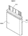
- FIG. 1 is a perspective view of a power semiconductor module according to Embodiment 1.
- FIG. The expanded view of the connector side lead assembly of this invention.
- the perspective view in the middle of manufacture of the power semiconductor module of this invention. The perspective view in the middle of manufacture of the power semiconductor module of this invention.
- the perspective view in the middle of manufacture of the power semiconductor module of this invention. The perspective view in the middle of manufacture of the power semiconductor module of this invention.
- FIG. The circuit diagram of the power semiconductor module of the present invention.
- FIG. 1 is a perspective view of a power semiconductor module 300 of this embodiment.
- the power semiconductor module 300 includes a sealing resin 900, DC side terminals 315B and 319B, an AC side terminal 320B, and signal terminals 325U, 325L, and 325S.
- the sealing resin 900 seals a power semiconductor element mounted on a metal conductor such as a lead frame or a ceramic substrate wiring.
- the terminals 315B, 319B, and 320B protrude from the one surface of the sealing resin 900 of the power semiconductor module 300 in a line.
- a sealing portion 901 is formed in the sealing resin 900 on the side from which these terminals protrude.
- the sealing resin 900 has a sealing resin surface 900A. A manufacturing procedure of the power semiconductor module 300 of the present embodiment will be described with reference to FIGS.
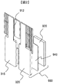
- FIG. 2 is a development view showing the arrangement relationship between the lead frame 315 and the lead frame 320 and the high thermal conductor 920.
- the lead frame 315 is connected to an upper arm IGBT 155 which is a power semiconductor element described later.
- the lead frame 320 is connected to a lower arm IGBT 157 that is a power semiconductor element described later.
- the lead frame 315 and the lead frame 320 are made of a conductive metal member such as copper.
- the IGBT is an abbreviation for an insulated gate bipolar transistor (Insulated Gate Bipolar Transistor).
- the high thermal conductor 920 is disposed on the opposite side of the lead frame 315 or the lead frame 320 with respect to the side to which the power semiconductor element is connected.
- the high thermal conductor 920 is provided corresponding to each lead frame.
- the high thermal conductor 920 is also disposed in a region facing the lead frame 315.
- An insulating layer 940 is disposed between the high thermal conductor 920 and the lead frame 315 and between the high thermal conductor 920 and the lead frame 320.
- the insulating layer 940 is a member disposed for the purpose of electrical insulation between the lead frame and the high thermal conductor.
- As the insulating layer 940 for example, an epoxy resin-based resin sheet filled with alumina particles and boron nitride particles is used.
- the high thermal conductor 920 is bonded to the lead frame through the insulating layer 940.
- the insulating layer was heat-pressed and cured using a vacuum press. The conditions used are, for example, thermocompression bonding at 200 ° C. for 2 hours at a pressure of 10 MPa in a reduced pressure atmosphere with a degree of vacuum of 1000 Pa or less.
- the lead frame 315 and the lead frame 320 are formed in a state where they are connected by a tie bar 912. Therefore, the high thermal conductor 920 and the lead frame are assembled as an integrated collector-side lead assembly 930 with the insulating layer 940 interposed therebetween.
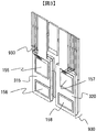
- FIG. 3 is a diagram showing a state in which the power semiconductor element is connected to the lead frame from the state of FIG.
- the IGBT 155 constituting the upper arm circuit of the inverter circuit is soldered to the lead frame 315.
- the diode 156 constituting the upper arm circuit of the inverter circuit is soldered to the lead frame 315.
- the IGBT 157 constituting the lower arm circuit of the inverter circuit is soldered to the lead frame 320.
- the diode 158 constituting the lower arm of the inverter circuit is soldered to the lead frame 320.
- the IGBTs 155 and 157 have signal electrodes formed on the surface on which the emitter electrode is formed. The signal electrode is electrically connected to the signal terminals 325L and 325L of the power semiconductor module 300 by an aluminum wire. Therefore, the IGBTs 155 and 157 are arranged closer to the signal terminal than the diodes 156 and 158.
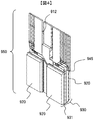
- FIG. 4 is a diagram showing a state in which the lead frame and the high thermal conductor 920 are arranged on the emitter side of the power semiconductor element from the state of FIG.
- the emitter side lead assembly 931 is formed in the same manner as the collector side lead assembly 930 in FIG.
- the emitter-side lead assembly 931 is disposed between the lead frame 318 connected to the emitter side of the IGBT 155, the lead frame 319 connected to the emitter side of the IGBT 157, the high thermal conductor 920, and the high thermal conductor and the lead frame.
- an insulating layer 940 is disposed between the lead frame 318 connected to the emitter side of the IGBT 155, the lead frame 319 connected to the emitter side of the IGBT 157, the high thermal conductor 920, and the high thermal conductor and the lead frame.
- an insulating layer 940 is an insulating layer 940.
- the temperature sensor 945 is bonded to the lead frame.
- the terminals of the temperature sensor 945 are welded to the signal terminals of the collector-side lead set 930.
- collector-side lead assembly 930 and the emitter-side lead assembly 931 are arranged with the power semiconductor element interposed therebetween.
- the assembly of the collector side lead assembly 930 and the emitter side lead assembly is referred to as a lead assembly 950.
- FIG. 5 is a diagram showing a process of transfer molding the lead assembly 950.
- the lead assembly 950 is set in the transfer mold 960 and 961, and the sealing resin 900 is injected.
- the mold temperature was 175 ° C.
- the molding pressure was 10 MPa
- the sealing resin 900 was cured in the mold for 3 minutes.
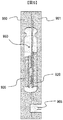
- FIG. 6 shows a lead assembly 950 that is transfer molded with a sealing resin 900.
- the high thermal conductor 920 is covered with a sealing resin 900.
- the sealing resin 900 has a sealing resin surface 900 ⁇ / b> A composed of substantially the same surface including a region covering the high thermal conductor 920.
- substantially the same surface represents a surface produced so as to be the same surface.
- the sealing resin surface 900A is caused by curing shrinkage of the sealing resin 900, thermal expansion difference between the sealing resin 900 and the internal structure such as the high thermal conductor 920, or the matte surface formed on the mold. Although it has a step of 100 ⁇ m or less, it is defined to be substantially the same plane.
- the tie bar 912 connecting the terminals is cut after transfer molding. Thereby, the terminals are electrically separated from each other.
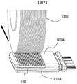
- FIG. 7 is a diagram illustrating a process of grinding the sealing resin surface 900A to form the fins 910A.
- the sealing resin surface 900A is ground by rotating the multi-blade 1300 at a high speed.
- the multi-blade 1300 has a structure in which a plurality of blades with abrasive grains at the tip are bundled.
- the multi-blade 1300 grinds the high thermal conductor 920 together with the sealing resin 900.
- the ground high thermal conductor 920 forms fins 910A.
- the groove depth between the fins is about 1.5 mm.
- the part to be ground generates heat due to frictional heat during grinding, so it is cooled by spraying cooling water. Further, the internal temperature is monitored using a temperature sensor 945 or the like provided inside the power semiconductor module, and the grinding speed is adjusted so that the internal temperature does not exceed 150 ° C. Thereby, remelting of the solder due to frictional heat can be prevented. Further, the fins 910A can be easily manufactured by grinding with a multi-blade.
- FIG. 8 is a cross-sectional view of the power semiconductor module 300. As shown in FIG. 8, the portion ground by the multi-blade 1300 in the procedure of FIG. 7 corresponds to the portion where the high thermal conductor 920 is disposed. In the power semiconductor module of the present embodiment, fins 910A are formed on both sides of the power semiconductor element.
- lead frames 319 and 320 are arranged with an IGBT 157 and a diode 158 on the lower arm side of the inverter circuit interposed therebetween.
- a high thermal conductor 920 is disposed on the opposite side of the lead frame 319 from the side on which the power semiconductor element is disposed.
- a high thermal conductor 920 is disposed on the opposite side of the lead frame 320 from the side on which the power semiconductor element is disposed.
- An insulating layer 940 is disposed between the high thermal conductor 920 and the lead frame.
- High heat conductor 920 forms fins 910A as a result of being ground together with sealing resin 900.
- the fins 910A are formed so that the tips of the fins are substantially flush with the sealing resin surface 910A, as indicated by the dotted lines in FIG.
- the fin 910A is formed from the heat dissipation surface formed to be concave with respect to the sealing resin surface 900A toward the side opposite to the side where the power semiconductor element is disposed.
- a sealing resin 900 is disposed at the tip of the fin 910A as indicated by reference numeral 910B.
- the tip of the fin is originally formed so as to be substantially flush with the sealing resin surface 910 ⁇ / b> A as shown in FIG. 6 as the sealing resin 900.
- the power semiconductor module 300 of the present embodiment described above is processed into a fin shape by grinding the resin sealing portion in which the high thermal conductor 920 is sealed.
- the heat radiation portion 910 is formed by a grinding method as shown in FIG. 7, but this may be realized by other machining. Since the periphery of the high thermal conductor 920 is sealed with the sealing resin 900, the high thermal conductor 920 is hardly peeled off even when the temperature changes. In addition, since the fin 910A is formed after resin sealing, the sealing resin 900 does not leak into the fin portion during the manufacturing process, and the yield is improved.
- a metal material having a high thermal conductivity or a carbon-containing material can be used as a material of the high thermal conductor 920.
- a metal material having a high thermal conductivity or a carbon-containing material can be used.
- copper, aluminum, copper carbon, aluminum carbon, graphene, or the like can be used.
- an aluminum-based material or a carbon-containing material it is easy to cut and has the effect of improving productivity.
- sealing resin 900 Although it does not specifically limit as a material of sealing resin 900, Transfer mold resin, potting resin, silicone resin, etc. can be used. When the transfer mold resin is used, the productivity is high and the external accuracy is high.
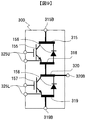
- FIG. 9 is a circuit diagram of the power semiconductor module of the present embodiment.
- the terminal 315B outputs from the collector side of the upper arm circuit, and is connected to the positive side of the battery or capacitor.
- the terminal 325U outputs from the gate and emitter sense of the IGBT 155 of the upper arm circuit.
- the terminal 319B outputs from the emitter side of the lower arm circuit, and is connected to the negative side of the battery or capacitor, or to GND.
- the terminal 325L outputs from the gate and emitter sense of the IGBT 157 of the lower arm circuit.
- the terminal 320B outputs from the collector side of the lower arm circuit and is connected to the motor. In the case of neutral point grounding, the lower arm circuit is connected to the negative electrode side of the capacitor instead of GND.
- the power semiconductor module of this embodiment has a 2-in-1 structure in which two arm circuits of an upper arm circuit and a lower arm circuit are integrated into one module.
- a 2-in-1 structure in which two arm circuits of an upper arm circuit and a lower arm circuit are integrated into one module.
- the number of output terminals from the power semiconductor module can be reduced and the size can be reduced.
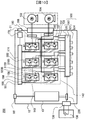
- FIG. 10 is a circuit diagram of a power conversion device using the power semiconductor module of the present embodiment.
- the power conversion device 200 includes inverter circuit units 140 and 142, an auxiliary inverter circuit unit 43, and a capacitor module 500.
- the inverter circuit units 140 and 142 include a plurality of power modules 300, and constitute a three-phase bridge circuit by connecting them. When the current capacity is large, the power modules 300 are further connected in parallel, and these parallel connections are made corresponding to the respective phases of the three-phase inverter circuit, so that an increase in the current capacity can be accommodated. Further, it is possible to cope with an increase in current capacity by connecting power semiconductor elements built in the power module 300 in parallel.
- the inverter circuit unit 140 and the inverter circuit unit 142 have the same basic circuit configuration and basically the same control method and operation.
- the inverter circuit unit 140 will be described as an example.
- the inverter circuit unit 140 includes a three-phase bridge circuit as a basic configuration. Specifically, each of the arm circuits operating as a U phase (indicated by a reference symbol U1), a V phase (indicated by a reference symbol V1), or a W phase (indicated by a reference symbol W1) transmits the DC power to the positive side and the negative side. Are connected in parallel with each other.
- the arm circuits operating as the U-phase, V-phase, and W-phase of the inverter circuit unit 142 are denoted by reference numerals U2, V2, and W2, as in the case of the inverter circuit unit 140.
- the arm circuit of each phase is composed of an upper and lower arm series circuit in which an upper arm circuit and a lower arm circuit are connected in series.
- the upper arm circuit of each phase is connected to the positive conductor, and the lower arm circuit of each phase is connected to the negative conductor.
- AC power is generated at the connection between the upper arm circuit and the lower arm circuit.
- a connection portion between the upper arm circuit and the lower arm circuit of each upper and lower arm series circuit is connected to an AC terminal 320 ⁇ / b> B of each power module 300.
- the AC terminal 320B of each power module 300 is connected to the AC output terminal of the power converter 200, and the generated AC power is supplied to the stator winding of the motor generator 192 or 194. Since each power module 300 of each phase has basically the same structure and basically the same operation, the U phase (U1) of the power module 300 will be described as a representative.
- the upper arm circuit includes an upper arm IGBT 155 and an upper arm diode 156 as power semiconductor elements for switching.
- the lower arm circuit includes a lower arm IGBT 157 and a lower arm diode 158 as power semiconductor elements for switching.
- the DC positive terminal 315B and the DC negative terminal 319B of each upper and lower arm series circuit are connected to the capacitor connecting DC terminal of the capacitor module 500, respectively.
- the AC power output from AC terminal 320B is supplied to motor generators 192 and 194.
- the IGBTs 155 and 157 perform a switching operation in response to a drive signal output from one or the other of the two driver circuits constituting the driver circuit 174, and convert DC power supplied from the battery 136 into three-phase AC power.
- the converted electric power is supplied to the stator winding of the motor generator 192. Since the V phase and the W phase have substantially the same circuit configuration as the U phase, the reference numerals 155, 156, 157, and 158 are omitted.
- the power module 300 of the inverter circuit unit 142 has the same configuration as that of the inverter circuit unit 140, and the inverter circuit unit 43 for auxiliary machines has the same configuration as the inverter circuit unit 142. Here, Description is omitted.
- the power semiconductor element for switching will be described using the upper arm IGBT 155 and the lower arm IGBT 157.
- the upper arm IGBT 155 and the lower arm IGBT 157 include a collector electrode, an emitter electrode (signal emitter electrode terminal), and a gate electrode (gate electrode terminal).
- An upper arm diode 156 and a lower arm diode 158 are electrically connected between the collector electrode and the emitter electrode of the upper arm IGBT 155 and the lower arm IGBT 157 as shown in the figure.
- the upper arm diode 156 and the lower arm diode 158 include two electrodes, a cathode electrode and an anode electrode.
- the cathode electrodes of the diodes 156 and 158 are the collector electrodes of the IGBTs 155 and 157
- the anode electrodes are the emitters of the IGBTs 155 and 157 so that the direction from the emitter electrode to the collector electrode of the upper arm IGBT 155 and the lower arm IGBT 157 is the forward direction.
- Each is electrically connected to the electrode.
- a MOSFET metal oxide semiconductor field effect transistor
- the upper arm diode 156 and the lower arm diode 158 are not necessary.
- Temperature information of the upper and lower arm series circuit is input to the microcomputer from a temperature sensor (not shown) provided in the upper and lower arm series circuit. Further, voltage information on the DC positive side of the upper and lower arm series circuit is input to the microcomputer. The microcomputer performs over temperature detection and over voltage detection based on the information, and when an over temperature or over voltage is detected, the switching operation of all the upper arm IGBT 155 and the lower arm IGBT 157 is stopped, and the upper and lower arms are connected in series. Protect the circuit from over temperature or over voltage.
- FIG. 11 is a perspective view showing an external appearance of the power conversion device 200.
- the external appearance of the power change device 200 according to the present embodiment is as follows.
- the housing 12 has a substantially rectangular top or bottom surface, the upper case 10 provided on one of the outer circumferences on the short side of the housing 12, and the housing 12.
- the lower case 16 for closing the lower opening is fixed and formed.
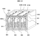
- FIG. 12 is a schematic diagram showing a cross-sectional structure of the power conversion device 200.
- the power semiconductor module 300 is installed in the flow path forming body 1000.
- the flow path forming body 1000 forms a coolant flow path through which a coolant that cools the power semiconductor module 300 flows.
- the flow path forming body 1000 has a wall surface 1001.
- the wall surface 1001 forms a flow path through which the coolant flows between the heat radiation part 910 of the power semiconductor module 300 and the wall surface 1001.
- the wall surface 1001 has a planar structure so that the coolant does not flow between the sealing resin surface 900A of the power semiconductor module 300 and the wall surface 1001.
- the distance between the opposing wall surfaces 1001 and the distance between the sealing resin surface 900A on one side and the sealing resin surface 900A on the other side of the power semiconductor module 300 are substantially equal.
- the seal portion 901 of the power semiconductor module 300 is provided with an elastic body such as an O-ring.
- the power conversion device 200 includes a laminated wiring board 501 and a plate 1200.
- the laminated wiring board 501 on which the mounting components are mounted is assembled, and the signal terminals and the laminated wiring board 501 are electrically connected. Further, the terminals 320B, 315B, and 320B through which a large current flows are welded to the terminals protruding from the plate 1200 in which the bus bar wiring is laminated in a multilayer manner. Since the laminated wiring board 501 and the plate can be three-dimensionally laminated, the power converter can be downsized.
- the power semiconductor module 300 is inserted into the flow path forming body 1000 so that the sealing resin surface 900A is in contact with the wall surface 1001 of the flow path forming body 1000.
- the power semiconductor module 300 is arranged such that the fin tips of the heat radiating portion 910 formed so as to be substantially flush with the sealing resin surface 900A are in contact with the wall surface 1001 of the flow path forming body 1000. Therefore, the refrigerant flowing between the heat radiation part 910 and the wall surface 1001 is suppressed from flowing as a bypass flow between the sealing resin surface 900A and the wall surface 1001, between the fin tip and the wall surface 1001, and the like. Since the heat radiating portion 910 is composed of the high thermal conductor 920 having high thermal conductivity, the heat of the power semiconductor element can be efficiently cooled. Therefore, the power semiconductor module 300 of this embodiment is excellent in reliability.
- the flow path through which the refrigerant flows is configured by a combination of a fin structure formed on the power semiconductor module 300 side and a wall surface 1001 on a plane formed on the flow path forming body 1000 side.
- the substantially same surface in the present embodiment means that the same surface is produced as much as possible. Steps that do not exceed 100 ⁇ m, such as steps caused by curing shrinkage of the resin and differences in thermal expansion between the members and surface roughness, have little influence on suppressing the bypass flow, and are therefore included in substantially the same plane.
- the flow path forming body 1000 is not particularly limited as long as it has a watertight structure, but is not limited to metals such as aluminum and aluminum die-cast, and thermoplastic resins such as polyphenylene sulfide, polybutylene terephthalate, polyamito, polyimide, and polytetrafluoroethylene. Or it can produce using thermosetting resins, such as an epoxy resin.
- FIG. 13 is a sectional view taken along section A in FIG.
- the housing 12 forms a flow path forming body 1000.
- the refrigerant flowing into the water channel 19 from the cooling water inlet 13 flows through the water channel 19 as indicated by an arrow, and is discharged from the cooling water outlet 14.
- six power semiconductor devices 300 are arranged in the water channel 19 along the flow of the cooling water.
- FIG. 14A is a perspective view showing a first modification of the power semiconductor module 300.
- the fin 910 ⁇ / b> A has a straight fin shape parallel to the refrigerant flow direction, but the fin 910 ⁇ / b> A in this embodiment has a rhombus shape.
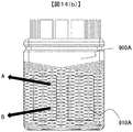
- FIG. 14B is a plan view showing the configuration of the heat radiating portion 910 of the power semiconductor module 300 of FIG.
- the fin shape is a pin fin, so that the heat dissipation can be improved as compared with the straight fin of FIG.
- FIG. 15A is a perspective view showing a second modification of the power semiconductor module 300.
- the fin 910 ⁇ / b> A has a straight fin shape parallel to the refrigerant flow direction, but the fin 910 ⁇ / b> A of the present embodiment has a quadrangular shape.
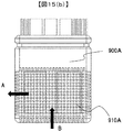
- FIG. 15B is a plan view showing the configuration of the heat radiating portion 910 of the power semiconductor module 300 of FIG.
- the sealing resin surface 900A of the power semiconductor module 300 is ground, the grinding is performed in the direction A in FIG. Thereby, a square-shaped pin fin can be formed.
- the fin shape is a pin fin, so that the heat dissipation can be improved as compared with the straight fin of FIG.
- the power semiconductor module of the above-described embodiment is not limited to the present embodiment, and after the electroless copper plating is applied to the surface in contact with the cooling water below the seal portion, the electroless nickel plating is applied. Thereby, it can prevent that sealing resin contacts a cooling water directly, and can suppress the fall of the chip insulation performance by the water absorption of sealing resin.
- FIG. 16A is a schematic diagram illustrating the relationship between the filling distance L of the sealing resin and the gap H.
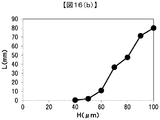
- FIG. 16B is a graph showing the filling distance L when the sealing resin is injected from the end of the gap with respect to the gap of thickness H.
- the filling distance L tends to increase as the gap H increases.
- the filling distance L was about several mm. From this, it can be seen that when the gap H is 50 ⁇ m or less, the sealing resin can hardly be filled.
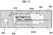
- FIG. 17 shows a cross-sectional view of the power semiconductor module 300 at the time of transfer molding.
- the sealing resin 900 of the power semiconductor module 300 is molded by transfer molding by setting the lead assembly 950 in the transfer mold 960 and 961.
- the high thermal conductor 920B of the lead assembly 950 arranged on the mold 961 side is pressed against the mold 961.
- the high thermal conductor 920A of the lead assembly 950 disposed on the mold 960 side is disposed with a gap H of 50 ⁇ m between the mold 960 and the high heat conductor 920A.
- the sealing resin 900 was not filled between the high thermal conductor 920A of the lead assembly 950 and the mold 960.
- the sealing resin 900 was not filled between the high thermal conductor 920 ⁇ / b> B of the lead assembly 950 and the mold 961.
- the high thermal conductors 920 ⁇ / b> A and 920 ⁇ / b> B could be molded while being exposed from the sealing resin 900 on both sides of the power semiconductor module.
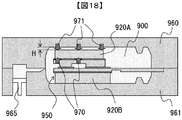
- FIG. 18 shows a case where the gap H between the lead assembly 950 and the mold 960 is set to 100 ⁇ m.
- the resin wraps around and fills the space between the high thermal conductor 920A and the mold 960.
- the lead assembly 950 is subjected to a stress that pushes up toward the mold 960 as indicated by an arrow 970.
- the lead assembly 950 is filled in the gap between the high thermal conductor 920A and the mold 960. Due to the sealing resin, downward stress as shown by an arrow 971 also acts.
- the hydrostatic pressure due to the sealing resin is balanced by wrapping and filling the sealing resin on one surface side of the lead assembly 950, excessive peeling stress is applied to the chip as shown in FIG. Adding is suppressed. Thereby, damage to the chip at the time of transfer molding can be suppressed, and the power semiconductor module can be manufactured with high reliability. Then, as shown in FIG. 7, the power semiconductor module is cut to form fins.
- FIG. 19 shows a cross-sectional perspective view of the power converter according to the second embodiment.
- the change point from the first embodiment is that the water channel formation body 1000 has a tapered shape, and the power semiconductor module also has a tapered shape corresponding to this.
- the taper shape facilitates the insertion of the power semiconductor module.
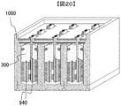
- FIG. 20 shows a cross-sectional perspective view of the power converter according to the third embodiment.
- the difference from the first embodiment is that ceramics are used for the insulating layer 940 of the power semiconductor module.
- the insulating property can be improved as compared with the resin sheet.
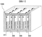
- FIG. 21 is a cross-sectional perspective view of the power conversion device according to the fourth embodiment.
- the changes from the first embodiment are that the water channel forming body 1000 is made of resin, the lead frame 911 of the power semiconductor module is a heat radiating portion, and there is no insulating layer 940, and the cooling medium is insulating oil. It is. Since insulating oil is used as a cooling medium, an insulating layer is not required inside the power semiconductor module, and the power converter can be downsized.
Landscapes
- Engineering & Computer Science (AREA)
- Microelectronics & Electronic Packaging (AREA)
- Power Engineering (AREA)
- Physics & Mathematics (AREA)
- Thermal Sciences (AREA)
- Inverter Devices (AREA)
- Manufacturing & Machinery (AREA)
- Cooling Or The Like Of Electrical Apparatus (AREA)
- Cooling Or The Like Of Semiconductors Or Solid State Devices (AREA)
Abstract
本発明の目的は、バイパス流を抑制し放熱性能に優れる電力変換装置を提供することである。本発明の電力変換装置は、パワー半導体モジュール300と、パワー半導体モジュール300が配置される流路形成体1000とを備え、パワー半導体モジュール300は、半導体チップと流路形成体1000に挟まれる位置に配置される高熱伝導体920と、パワー半導体素子及び高熱伝導体920を封止する封止材とを有し、高熱伝導体920は、流路形成体1000側に流路形成体1000に向かって突出するフィンを有し、フィンを囲む封止材の一部とフィン先端が概略同一平面にある事を特徴とする。
Description
本発明はパワー半導体モジュール及びこれを用いた電力変換装置に関する。
パワー半導体素子のスイッチングによる電力変換装置は、変換効率が高いため、民生用、車載用、鉄道用、変電設備等に幅広く利用されている。このパワー半導体素子は通電により発熱するため、高い放熱性が求められる。また、パワー半導体素子は絶縁性のため樹脂又はゲルで封止される。
パワー半導体素子を流路形成した金属体に搭載して樹脂封止する構造として、特許文献1が開示されている。
特許文献1に記載された半導体装置では、あらかじめ水密性能を確保した水路にパワー半導体素子をはんだ接続し、樹脂封止するため、製造過程で温度や圧力が加わり水密性能が低下する可能性があった。
本発明の目的は、バイパス流を抑制した放熱効率の高いパワー半導体モジュールの形成を容易とし、電力変換装置の信頼性向上を図るものである。
本発明の電力変換装置は、直流電流を交流電流に変換するパワー半導体素子を有するパワー半導体モジュールと、前記パワー半導体モジュールが配置される流路形成体と、を備え、前記パワー半導体モジュールは、前記半導体チップと前記流路形成体に挟まれる位置に配置される高熱伝導体と、前記パワー半導体素子と前記高熱伝導体を封止する封止材とを有し、前記高熱伝導体は、前記流路形成体側に当該流路形成体に向かって突出するフィンを有し、前記フィンを囲む封止材の一部と前記フィン先端が概略同一平面にある事を特徴とする。
本発明によれば、パワー半導体モジュール及び流路の形成が容易でありながら、バイパス流を抑制し高放熱、効率的にフィンに水流が誘導でき、高放熱化できる。
以下、図面を参照して、本発明に係るパワー半導体モジュール及び電力変換装置の実施の形態について説明する。なお、各図において同一要素については同一の符号を記し、重複する説明は省略する。
図1は、本実施形態のパワー半導体モジュール300の斜視図である。パワー半導体モジュール300は、封止樹脂900と、直流側の端子315B及び319Bと、交流側の端子320Bと、信号用の端子325U、325L、325Sを有する。封止樹脂900は、リードフレームやセラミックス基板配線等の金属導体に搭載したパワー半導体素子を封止する。端子315B、319B、320Bは、パワー半導体モジュール300の封止樹脂900の一面から一列に突出している。これらの端子が突出する側の封止樹脂900には、シール部901が形成される。後述するように、パワー半導体モジュール300は、流路形成体1000に固定される際に、シール部901に配置されたOリング等の部材により、冷却冷媒の気密性を確保する。また、封止樹脂900は、封止樹脂面900Aを有する。本実施例のパワー半導体モジュール300の製造手順について、図2から図7を用いて説明する。
図2は、リードフレーム315及びリードフレーム320と、高熱伝導体920の配置関係を示す展開図である。リードフレーム315には、後述するパワー半導体素子である上アーム側IGBT155が接続される。リードフレーム320には、後述するパワー半導体素子である下アーム側IGBT157が接続される。リードフレーム315及びリードフレーム320は、導電性の金属部材、例えば銅により構成される。ここで、IGBTとは、絶縁ゲート型バイポーラトランジスタ(Insulated Gate Bipolar Transistor)の略である。
高熱伝導体920は、リードフレーム315又はリードフレーム320を挟んで、パワー半導体素子が接続される側とは反対側に配置される。高熱伝導体920は、各リードフレームに対応して、設けられる。図2には図示されないが、リードフレーム315と対向する領域にも、高熱伝導体920は配置される。
高熱伝導体920とリードフレーム315の間、及び高熱伝導体920とリードフレーム320の間には、絶縁層940が配置される。絶縁層940は、リードフレームと高熱伝導体との間の電気的な絶縁を目的として配置される部材である。絶縁層940としては、例えば、アルミナ粒子及び窒化ホウ素粒子を充填したエポキシ樹脂系の樹脂シートが用いられる。高熱伝導体920は、絶縁層940を介してリードフレームに接着される。絶縁層は、真空プレス機を用いて加熱圧着し、硬化させた。用いる条件は、例えば、真空度が1000Pa以下の減圧雰囲気下にて、10MPaの圧力で、200℃、2時間の加熱圧着とする。
リードフレーム315とリードフレーム320とは、タイバー912により接続された状態で形成される。そのため、高熱伝導体920及び当該リードフレームは、絶縁層940を挟んで、一体のコレクタ側リード組み930として組み立てられる。
図3は、図2の状態から、パワー半導体素子をリードフレームに接続した状態を示す図である。インバータ回路の上アーム回路を構成するIGBT155は、リードフレーム315に対して、はんだ接続される。インバータ回路の上アーム回路を構成するダイオード156は、リードフレーム315に対して、はんだ接続される。インバータ回路の下アーム回路を構成するIGBT157は、リードフレーム320に対して、はんだ接続される。インバータ回路の下アームを構成するダイオード158は、リードフレーム320に対して、はんだ接続される。IGBT155及び157は、エミッタ電極が形成される側の面において、信号用電極が形成されている。当該信号電極は、パワー半導体モジュール300の信号端子325L及び325Lと、アルミワイヤにより電気的に接続される。そのため、IGBT155及び157は、ダイオード156及び158よりも、信号端子に近い位置に配置される。
図4は、図3の状態から、パワー半導体素子のエミッタ側にリードフレーム及び高熱伝導体920を配置した状態を示す図である。手順としては、まず、図2においてコレクタ側リード組930を形成したのと同様にして、エミッタ側リード組み931を形成する。エミッタ側リード組み931は、IGBT155のエミッタ側に接続されるリードフレーム318と、IGBT157のエミッタ側に接続されるリードフレーム319と、高熱伝導体920と、高熱伝導体とリードフレームの間に配置される絶縁層940と、により構成される。
また、温度センサ945がリードフレームに接着される。当該温度センサ945の端子は、コレクタ側リード組930の信号端子に溶接される。温度センサ945が設けられることで、機械加工によってフィンを形成する時の発熱をモニタし、規定値を超えた温度とならないように管理することができる。
このようにして、コレクタ側リード組み930と、エミッタ側リード組み931とを、パワー半導体素子を挟んで配置される。コレクタ側リード組み930とエミッタ側リード組みを組み立てたものを、リード組立体950とする。
図5は、リード組立体950をトランスファーモールドする工程を示す図である。リード組立体950は、トランスファーモールド金型960及び961にセットされ、封止樹脂900が注入される。金型温度は175℃、成型圧力は10MPaとし、金型内で3分間、封止樹脂900を硬化させた。
図6は、リード組立体950を封止樹脂900でトランスファーモールドしたものを示す。高熱伝導体920は、封止樹脂900で覆われている。封止樹脂900は、高熱伝導体920を覆う領域を含め、概略同一面からなる封止樹脂面900Aを有する。ここで、概略同一面とは、同一面となるように作製した面を表す。具体的には、封止樹脂面900Aは、封止樹脂900の硬化収縮、封止樹脂900と高熱伝導体920等の内部構造との熱膨張差、または金型に形成した梨地表面などによって、100μm以下の段差を有するが、概略同一面であると定義される。
端子同士を接続するタイバー912は、トランスファーモールド後に切断される。これにより、端子同士は、互いに電気的に分離される。
図7は、封止樹脂面900Aを研削してフィン910Aを形成する工程を示す図である。封止樹脂面900Aは、マルチブレード1300を高速回転させることによって、研削される。マルチブレード1300は、先端に砥粒を付けた複数のブレードを束ねた構造である。マルチブレード1300は、封止樹脂900とともに、高熱伝導体920を研削する。研削された高熱伝導体920は、フィン910Aを形成する。フィン間の溝深さは、約1.5mmとなる。
研削される部分は、研削時に摩擦熱によって発熱するため、冷却水を噴射して冷却する。また、パワー半導体モジュール内部に設けた温度センサ945等を用いて内部温度をモニタし、内部温度が150℃を超えないように、研削速度を調整する。これにより、摩擦熱によるはんだの再溶融を防ぐことができる。また、マルチブレードで研削することにより、容易にフィン910Aを作製することができる。
図8は、パワー半導体モジュール300の断面図である。図8図示されるように、図7の手順でマルチブレード1300によって研削される部分は、高熱伝導体920が配置される部分と対応する。本実施例のパワー半導体モジュールにおいては、パワー半導体素子の両面側において、フィン910Aが形成される。
図8は、インバータ回路の下アーム側のIGBT157及びダイオード158を挟んで、リードフレーム319及び320が配置されている。リードフレーム319を挟んで、パワー半導体素子が配置される側とは反対側には、高熱伝導体920が配置される。同様に、リードフレーム320を挟んで、パワー半導体素子が配置される側とは反対側に、高熱伝導体920が配置される。高熱伝導体920と、リードフレームの間には、絶縁層940が配置される。
高熱伝導体920は、封止樹脂900とともに研削された結果、フィン910Aを形成している。フィン910Aは、図8の点線で示されるように、当該フィンの先端が封止樹脂面910Aと概略同一面上となるように、形成されている。言い換えれば、フィン910Aは、封止樹脂面900Aに対して凹となるように形成された放熱面から、パワー半導体素子が配置される側とは反対側に向かって形成されている。
また、フィン910Aは、図7に示されるように形成されるため、当該フィン910Aの先端には、符号910Bで示されるように封止樹脂900が配置されている。このように、フィン先端は、もともと封止樹脂900として図6に示されるように、封止樹脂面910Aと概略同一面上となるように形成されている。
以上説明した本実施形態のパワー半導体モジュール300は、高熱伝導体920を封止した樹脂封止部を研削することで、フィン形状に加工される。なお、本実施例では、図7に示されるような研削による方法によって放熱部910を形成したが、他の機械加工でこれを実現しても良い。高熱伝導体920は、その周囲が封止樹脂900によって封止されているため、温度変化が加わっても剥離されにくい。また、樹脂封止した後にフィン910Aの形成加工をするため、製造の過程において、封止樹脂900がフィン部に漏れ出すことがなく、歩留まりが向上する。
高熱伝導体920の材料としては、熱伝導率の高い金属材料や、カーボン含有材料を用いる事ができる。例えば、銅、アルミ、銅カーボン、アルミカーボン、グラフェン等を用いることができる。アルミ系材料やカーボン含有材料を用いた場合、切削加工しやすく生産性が向上する効果がある。
封止樹脂900の材料としては、特に限定されないが、トランスファーモールド樹脂、ポッティング樹脂、シリコーン樹脂等を用いることができる。トランスファーモールド樹脂を用いた場合、生産性が高く、外形精度が高い効果がある。
図9は、本実施形態のパワー半導体モジュールの回路図である。端子315Bは、上アーム回路のコレクタ側から出力しており、バッテリー又はコンデンサの正極側に接続される。端子325Uは、上アーム回路のIGBT155のゲート及びエミッタセンスから出力している。端子319Bは、下アーム回路のエミッタ側から出力しており、バッテリー若しくはコンデンサの負極側、又はGNDに接続される。端子325Lは、下アーム回路のIGBT157のゲート及びエミッタセンスから出力している。端子320Bは、下アーム回路のコレクタ側から出力しており、モータに接続される。中性点接地をする場合は、下アーム回路は、GNDでなくコンデンサの負極側に接続する。
本実施例のパワー半導体モジュールは、上アーム回路及び下アーム回路の2つのアーム回路を、1つのモジュールに一体化した構造である2in1構造である。2in1構造の他にも、3in1構造、4in1構造、6in1構造等を用いた場合、パワー半導体モジュールからの出力端子の数を低減し小型化することができる。
図10は、本実施例のパワー半導体モジュールを用いた電力変換装置の回路図である。電力変換装置200は、インバータ回路部140、142と、補機用のインバータ回路部43と、コンデンサモジュール500と、を備えている。インバータ回路部140及び142は、パワーモジュール300を複数備えており、それらを接続することにより3相ブリッジ回路を構成している。電流容量が大きい場合には、更にパワーモジュール300を並列接続し、これら並列接続を3相インバータ回路の各相に対応して行うことにより、電流容量の増大に対応できる。また、パワーモジュール300に内蔵しているパワー半導体素子を並列接続することでも電流容量の増大に対応できる。
インバータ回路部140とインバータ回路部142とは、基本的な回路構成は同じであり、制御方法や動作も基本的には同じである。ここでは代表してインバータ回路部140を例に説明する。インバータ回路部140は、3相ブリッジ回路を基本構成として備えている。具体的には、U相(符号U1で示す)やV相(符号V1で示す)やW相(符号W1で示す)として動作するそれぞれのアーム回路が、直流電力を送電する正極側および負極側の導体にそれぞれ並列に接続されている。なお、インバータ回路部142のU相、V相およびW相として動作するそれぞれのアーム回路を、インバータ回路部140の場合と同様に、符号U2、V2およびW2で示す。
各相のアーム回路は、上アーム回路と下アーム回路とが直列に接続した上下アーム直列回路で構成されている。各相の上アーム回路は正極側の導体にそれぞれ接続され、各相の下アーム回路は負極側の導体にそれぞれ接続されている。上アーム回路と下アーム回路の接続部には、それぞれ交流電力が発生する。各上下アーム直列回路の上アーム回路と下アーム回路の接続部は、各パワーモジュール300の交流端子320Bに接続されている。各パワーモジュール300の交流端子320Bはそれぞれ電力変換装置200の交流出力端子に接続され、発生した交流電力はモータジェネレータ192あるいは194の固定子巻線に供給される。各相の各パワーモジュール300は基本的に同じ構造であり、動作も基本的に同じであるので、代表してパワーモジュール300のU相(U1)について説明する。
上アーム回路は、スイッチング用のパワー半導体素子として上アーム用IGBT155と上アーム用ダイオード156とを備えている。また、下アーム回路は、スイッチング用のパワー半導体素子として下アーム用IGBT157と下アーム用ダイオード158とを備えている。各上下アーム直列回路の直流正極端子315Bおよび直流負極端子319Bは、コンデンサモジュール500のコンデンサ接続用直流端子にそれぞれ接続される。交流端子320Bから出力される交流電力は、モータジェネレータ192、194に供給される。
IGBT155及び157は、ドライバ回路174を構成する2つのドライバ回路の一方あるいは他方から出力された駆動信号を受けてスイッチング動作し、バッテリー136から供給された直流電力を三相交流電力に変換する。変換された電力は、モータジェネレータ192の固定子巻線に供給される。なお、V相およびW相については、U相と略同じ回路構成となるので、符号155、156、157、158の表示を省略している。インバータ回路部142のパワーモジュール300は、インバータ回路部140の場合と同様の構成であり、また、補機用のインバータ回路部43はインバータ回路部142と同様の構成を有しており、ここでは説明を省略する。
スイッチング用のパワー半導体素子について、上アーム用IGBT155および下アーム用IGBT157を用いて説明する。上アーム用IGBT155や下アーム用IGBT157は、コレクタ電極、エミッタ電極(信号用エミッタ電極端子)、ゲート電極(ゲート電極端子)を備えている。上アーム用IGBT155や下アーム用IGBT157のコレクタ電極とエミッタ電極との間には、上アーム用ダイオード156や下アーム用ダイオード158が図示のように電気的に接続されている。
上アーム用ダイオード156や下アーム用ダイオード158は、カソード電極およびアノード電極の2つの電極を備えている。上アーム用IGBT155や下アーム用IGBT157のエミッタ電極からコレクタ電極に向かう方向が順方向となるように、ダイオード156、158のカソード電極がIGBT155、157のコレクタ電極に、アノード電極がIGBT155、157のエミッタ電極にそれぞれ電気的に接続されている。なお、パワー半導体素子としてはMOSFET(金属酸化物半導体型電界効果トランジスタ)を用いても良く、この場合は上アーム用ダイオード156、下アーム用ダイオード158は不要となる。
上下アーム直列回路に設けられた温度センサ(不図示)からは、上下アーム直列回路の温度情報がマイコンに入力される。また、マイコンには上下アーム直列回路の直流正極側の電圧情報が入力される。マイコンは、それらの情報に基づいて過温度検知および過電圧検知を行い、過温度或いは過電圧が検知された場合には全ての上アーム用IGBT155、下アーム用IGBT157のスイッチング動作を停止させ、上下アーム直列回路を過温度或いは過電圧から保護する。
図11は、電力変換装置200の外観を示す斜視図である。本実施の形態に係る電力変化装置200の外観は、上面あるいは底面が略長方形の筐体12と、筐体12の短辺側の外周の一つに設けられた上部ケース10と、筐体12の下部開口を塞ぐための下部ケース16とを固定して形成されたものである。筐体12の底面図あるいは上面図の形状を略長方形としたことで、車両への取付けが容易となり、また生産しやすい。
図12は、電力変換装置200の断面構造を示す概略図である。パワー半導体モジュール300は、流路形成体1000に設置される。流路形成体1000は、パワー半導体モジュール300を冷却する冷媒を流す冷媒流路を形成する。流路形成体1000は、壁面1001を有する。壁面1001は、パワー半導体モジュール300の放熱部910と当該壁面1001との間に、冷媒が流れる流路を形成する。壁面1001は、パワー半導体モジュール300の封止樹脂面900Aと当該壁面1001との間に冷媒が流れないように、平面構造を有する。流路形成体1000は、互いに対向する壁面1001同士の距離と、パワー半導体モジュール300の一方側の封止樹脂面900Aと他方側の封止樹脂面900Aの間の距離とが、ほぼ等しくなるように、形成される。パワー半導体モジュール300のシール部901には、Oリング等の弾性体が設けられる。
電力変換装置200は、積層配線板501及びプレート1200とを有する。
パワー半導体モジュール300を流路形成体に挿入した後、実装部品を搭載した積層配線板501を組み付け、信号端子と積層配線板501を電気的に接続する。さらに、大電流が流れる端子320B、315B、320Bはバスバー配線を多層積層したプレート1200から突出した端子と溶接する。積層配線板501とプレートを立体積層することができるため、電力変換装置を小型化することができる。
パワー半導体モジュール300は、封止樹脂面900Aが流路形成体1000の壁面1001と接するように、流路形成体1000に対して挿入される。これにより、パワー半導体モジュール300は、封止樹脂面900Aと概略同一面となるように形成された放熱部910のフィン先端が流路形成体1000の壁面1001と当接するように、配置される。したがって、放熱部910と壁面1001の間に流れる冷媒は、封止樹脂面900Aと壁面1001の間や、フィン先端と壁面1001の間などにバイパス流として流れることが抑制される。放熱部910は、高い熱伝導率である高熱伝導体920で構成されるため、効率的にパワー半導体素子の熱を冷却することができる。したがって、本実施形態のパワー半導体モジュール300は、信頼性に優れる。
また、冷媒が流れる流路は、パワー半導体モジュール300側に形成されたフィン構造と、流路形成体1000側に形成された平面上に壁面1001との組合せによって、構成される。このように構造を簡略化することで、電力変換装置の製造が容易になる。
また、前述したように、本実施形態における概略同一面とは、同一面となるべく作製した事を意味している。樹脂の硬化収縮や部材間の熱膨張差により生じた段差及び表面粗さ等の100μmを越えない段差は、バイバス流を抑制する上で影響が少ないため、概略同一面に含まれるものとする。
流路形成体1000は、水密構造を有するものであれば特に限定されないが、アルミ、アルミダイキャスト等の金属や、ポリフェニレンサルファイド、ポリブチレンテレフタレート、ポリアミト、ポリイミド、ポリテトラフルオロエチレン等の熱可塑性樹脂や、エポキシ樹脂等の熱硬化性樹脂を用いて作製することができる。
図13は、図11の断面Aにおける断面図である。筐体12は、流路形成体1000を形成する。冷却水入口13から水路19内に流入した冷媒は、水路19を矢印で示すように流れ、冷却水出口14から排出される。本実施形態においては、水路19内に、6つのパワー半導体装置300が冷却水の流れに沿って配置されている。
図14(a)は、パワー半導体モジュール300の第1の変形例を示す斜視図である。図1のパワー半導体モジュールにおいては、フィン910Aの形状は、冷媒の流れる方向に対して平行なストレートフィン形状に形成されていたが、本実施例のフィン910Aの形状は、ひし形形状である。
また、図14(b)は、図14(a)のパワー半導体モジュール300の放熱部910の構成を示す平面図である。本実施例では、パワー半導体モジュール300の封止樹脂面900Aを研削するときに、図7とは異なり、図14(b)の方向Aで研削し、さらに方向Bで研削する。これにより、ひし形形状のピンフィンを形成することができる。本実施形態の放熱部910のように、フィンの形状をピンフィンにすることで、図1のストレートフィンに比較して、放熱性が向上することができる。
図15(a)は、パワー半導体モジュール300の第2の変形例を示す斜視図である。図1のパワー半導体モジュールにおいては、フィン910Aの形状は、冷媒の流れる方向に対して平行なストレートフィン形状に形成されていたが、本実施例のフィン910Aの形状は、四角形形状である。
また、図15(b)は、図14(a)のパワー半導体モジュール300の放熱部910の構成を示す平面図である。本実施例では、パワー半導体モジュール300の封止樹脂面900Aを研削するときに、図7とは異なり、図15(b)の方向Aで研削し、さらに方向Bで研削する。これにより、四角形形状のピンフィンを形成することができる。本実施形態の放熱部910のように、フィンの形状をピンフィンにすることで、図1のストレートフィンに比較して、放熱性が向上することができる。
また、本実施例に限らず、上述の実施形態のパワー半導体モジュールは、シール部以下の冷却水が接する表面に無電解銅めっきを施した後、無電解ニッケルめっきを施される。これにより、封止樹脂が直接冷却水に接するのを防ぎ、封止樹脂の吸水によるチップ絶縁性能の低下を抑制することができる。
次に、封止樹脂の充填距離Lと隙間Hとの関係について説明する。図16(a)は、封止樹脂の充填距離Lと隙間Hの関係を模式図である。また、図16(b)は、厚さHの隙間に対し、封止樹脂を隙間の端部から注入した際の充填距離Lを示すグラフである。
図16(b)に示されるように、隙間Hが大きくなるほど、充填距離Lが大きくなる傾向が見られる。また、隙間Hが50μm以下の場合においては、充填距離Lは数mm程度となった。これより、隙間Hが50μm以下の場合は、封止樹脂をほとんど充填することができないことが分かる。
図17は、トランスファーモールド成型時におけるパワー半導体モジュール300の断面図を示す。パワー半導体モジュール300の封止樹脂900は、リード組立体950をトランスファーモールド金型960及び961内にセットし、トランスファーモールドにより成型される。その際、金型961側に配置されるリード組立体950の高熱伝導体920Bは、金型961に押し付けられている。
図17においては、金型960側に配置されるリード組立体950の高熱伝導体920Aは、金型960との間に50μmの隙間Hを隔てて配置される。リード組立体950と金型960の間の隙間を50μmとした場合、リード組立体950の高熱伝導体920Aと金型960との間には、封止樹脂900は充填されなかった。また、リード組立体950の高熱伝導体920Bと金型961との間にも、封止樹脂900は充填されなかった。この結果、パワー半導体モジュールの両面側において、高熱伝導体920A及び920Bは、封止樹脂900から露出した状態で成型することができた。
しかしながら、このようにして作製したパワー半導体モジュール300は、トランスファーモールド時の成型圧力により、チップのメタライズに剥離応力が加わるため、チップが破損するなど信頼性を向上させることが難しい。このような剥離応力は、トランスファーモールド時の成型圧力が樹脂硬化前の段階では静水圧として作用し、図中に示される矢印970のように、リード組立体950を押し上げる応力として生じる。このようにして、チップに強力な剥離応力が加わったことにより、チップのメタライズが剥離するおそれが生じる。
続いて、図18に、リード組立体950と金型960との間の隙間Hを100μmに設定した場合を示す。リード組立体950と金型の間の隙間Hを100μmとすることで、高熱伝導体920Aと金型960の間には、樹脂が回り込み、充填される結果となった。
このとき、リード組立体950には、図17と同様に、矢印970のように金型960に向かって押し上げる応力が作用するが、同時に、高熱伝導体920Aと金型960の隙間に充填された封止樹脂により、矢印971のように下向きの応力も作用する。このように、リード組立体950の一方の面側において、封止樹脂を回り込ませて充填させることで、封止樹脂による静水圧が釣り合うため、図17に示すように過度の剥離応力がチップに加わることが抑制される。これにより、トランスファーモールド成型時におけるチップの破損を抑制し、パワー半導体モジュールを高い信頼性をもって作製することができる。パワー半導体モジュールは、その後、図7に示すように、切削加工を施すことにより、フィンが形成される。
図19は、第2の実施形態に係る電力変換装置の断面斜視図を示す。第1の実施形態との変化点は、水路形成体1000がテーパ形状となっており、これに対応してパワー半導体モジュールもテーパ形状になっている点である。テーパ形状となっている事で、パワー半導体モジュールの挿入が容易となる。
図20は、第3の実施形態に係る電力変換装置の断面斜視図を示す。第1の実施形態との変化点は、パワー半導体モジュールの絶縁層940にセラミックスを用いている点である。絶縁層がセラミックスの基板を用いる事で、樹脂シートに比べて絶縁性が向上することができる。
図21は、第4の実施形態に係る電力変換装置の断面斜視図を示す。第1の実施形態との変化点は、水路形成体1000が樹脂製である点、パワー半導体モジュールのリードフレーム911が放熱部となり絶縁層940が無い点、及び冷却媒体が絶縁性油である点である。絶縁性油を冷却媒体に用いているため、パワー半導体モジュール内部に絶縁層が不要であり、電力変換装置を小型化することができる。
10 上部ケース
12 筺体
13 冷却水入口
14 冷却水出口
16 下部ケース
18 交流ターミナル
19 流路
22 駆動回路基板
43 インバータ回路
110 ハイブリッド自動車
112 前輪
114 前輪車軸
116 デファレンシャルギア
118 変速機
120 エンジン
122 動力配分機構
136 バッテリ
138 直流コネクタ
140 インバータ回路
142 インバータ回路
155 上アーム用IGBT
156 ダイオード
157 下アーム用IGBT
172 制御回路
174 ドライバ回路
180 電流センサ
192 モータジェネレータ
194 モータジェネレータ
195 モータ
200 電力変換装置
230 入力積層配線板
300 パワー半導体装置
321 交流端子
500 コンデンサモジュール
501 積層配線板
505 負極電極リードフレーム
507 正極電極リードフレーム
514 コンデンサセル
702 正極側電極リードフレーム
704 負極側電極リードフレーム
900 封止樹脂
900A 封止樹脂面
901 シール部
910 放熱部
919A フィン
911 リードフレーム
912 タイバー
920 高熱伝導体
920A 高熱伝導体
920B 高熱伝導体
930 コレクタ側リード組み
931 エミッタ側リード組み
940 絶縁層
945 温度センサ
950 リード組立体
960 トランスファーモールド金型
961 トランスファーモールド金型
965 プランジャー
1000 流路形成体
1001 壁面
1200 プレート
Claims (9)
- 直流電流を交流電流に変換するパワー半導体素子を有するパワー半導体モジュールと、
前記パワー半導体モジュールが配置される流路形成体とを備え、
前記パワー半導体モジュールは、前記半導体チップと前記流路形成体に挟まれる位置に配置される高熱伝導体と、前記パワー半導体素子及び前記高熱伝導体を封止する封止材とを有し、
前記高熱伝導体は、前記流路形成体側に当該流路形成体に向かって突出するフィンを有し、
前記フィンを囲む前記封止材の一部と前記フィン先端が概略同一平面にある事を特徴とする電力変換装置。 - 請求項1に記載の電力変換装置であって、
前記高熱伝導体の前記フィンは、当該フィンの先端が前記封止材と同じ材料となるように、形成されている電力変換装置。 - 請求項1又は2のいずれかに記載の電力変換装置であって、
前記フィンは、前記高熱伝導体を封止する前記封止材を溝状に研削することにより、形成される電力変換装置。 - 請求項1乃至3のいずれかに記載の電力変換装置であって、
前記封止材は、前記パワー半導体モジュールが前記流路形成体に配置された際に流路の気密を確保するためのシール部を有する電力変換装置。 - 請求項3に記載の電力変換装置であって、
前記フィンは、ピンフィン形状に形成される電力変換装置・ - 請求項1乃至5のいずれかに記載の電力変換装置であって、
前記高熱伝導体は、カーボン含有材料により形成される電力変換装置。 - 請求項1乃至6のいずれかに記載の電力変換装置であって、
前記封止材は、前記流路形成体の流路側の表面がめっきされている電力変換装置。 - 直流電流を交流電流に変換するパワー半導体素子と、前記半導体チップと熱的に接続される高熱伝導体と、前記パワー半導体素子及び前記高熱伝導体を封止する封止材と、を備えたパワー半導体モジュールの製造方法であって、
前記高熱伝導体を前記封止材で封止する第1工程と、
前記封止材及び前記高熱伝導体を一体加工して、先端が前記封止材の一部と概略同一平面となるフィンを形成する第2工程と、を有するパワー半導体モジュールの製造方法。 - 請求項8に記載のパワー半導体モジュールの製造方法であって、
前記第1工程において、前記封止材は、前記高熱伝導体の前記パワー半導体素子が配置される側とは反対側の面を覆って封止されるパワー半導体モジュールの製造方法。
Priority Applications (3)
| Application Number | Priority Date | Filing Date | Title |
|---|---|---|---|
| DE112015003295.9T DE112015003295T5 (de) | 2014-09-09 | 2015-06-08 | Leistungsumsetzungsvorrichtung |
| US15/500,391 US10194563B2 (en) | 2014-09-09 | 2015-06-08 | Power conversion device |
| CN201580048565.XA CN106716813B (zh) | 2014-09-09 | 2015-06-08 | 电力转换装置 |
Applications Claiming Priority (2)
| Application Number | Priority Date | Filing Date | Title |
|---|---|---|---|
| JP2014-182844 | 2014-09-09 | ||
| JP2014182844A JP6302803B2 (ja) | 2014-09-09 | 2014-09-09 | パワー半導体モジュール及びその製造方法、電力変換装置 |
Publications (1)
| Publication Number | Publication Date |
|---|---|
| WO2016038956A1 true WO2016038956A1 (ja) | 2016-03-17 |
Family
ID=55458719
Family Applications (1)
| Application Number | Title | Priority Date | Filing Date |
|---|---|---|---|
| PCT/JP2015/066428 Ceased WO2016038956A1 (ja) | 2014-09-09 | 2015-06-08 | 電力変換装置 |
Country Status (5)
| Country | Link |
|---|---|
| US (1) | US10194563B2 (ja) |
| JP (1) | JP6302803B2 (ja) |
| CN (1) | CN106716813B (ja) |
| DE (1) | DE112015003295T5 (ja) |
| WO (1) | WO2016038956A1 (ja) |
Cited By (1)
| Publication number | Priority date | Publication date | Assignee | Title |
|---|---|---|---|---|
| US20220244111A1 (en) * | 2021-02-01 | 2022-08-04 | Fuji Electric Co., Ltd. | Semiconductor device and temperature measurement method |
Families Citing this family (17)
| Publication number | Priority date | Publication date | Assignee | Title |
|---|---|---|---|---|
| US10137798B2 (en) * | 2015-08-04 | 2018-11-27 | Ford Global Technologies, Llc | Busbars for a power module assembly |
| WO2017215161A1 (zh) * | 2016-06-16 | 2017-12-21 | 广东合一新材料研究院有限公司 | 一种用于计算机及数据中心散热的工质接触式冷却系统 |
| JP6635901B2 (ja) * | 2016-09-21 | 2020-01-29 | 本田技研工業株式会社 | 電力変換装置 |
| JP6673118B2 (ja) * | 2016-09-23 | 2020-03-25 | 株式会社デンソー | 半導体装置 |
| WO2018110513A1 (ja) * | 2016-12-15 | 2018-06-21 | 株式会社村田製作所 | 能動素子、高周波モジュールおよび通信装置 |
| CN108988654B (zh) * | 2017-05-31 | 2020-06-26 | 中车株洲电力机车研究所有限公司 | 一种逆变器模块 |
| JP6743782B2 (ja) * | 2017-08-11 | 2020-08-19 | 株式会社デンソー | 電力変換装置 |
| DE102018201262B4 (de) * | 2018-01-29 | 2022-10-13 | Zf Friedrichshafen Ag | Ein Verfahren zum Herstellen eines Pin-Fin-Leistungsmoduls |
| JP7087850B2 (ja) | 2018-09-05 | 2022-06-21 | 株式会社デンソー | 半導体装置 |
| WO2021197409A1 (en) * | 2020-04-01 | 2021-10-07 | Atlas Copco (Wuxi) Compressor Co., Ltd. | Inverter power assembly |
| JP7444711B2 (ja) * | 2020-06-24 | 2024-03-06 | 株式会社日立製作所 | パワーモジュール及びこれを用いた電力変換装置 |
| CN112310017B (zh) * | 2020-09-30 | 2022-04-26 | 东风汽车集团有限公司 | 一种半导体器件散热结构 |
| CN116190360B (zh) | 2021-11-26 | 2024-09-10 | 比亚迪股份有限公司 | 功率模块和电器设备 |
| DE102022116921A1 (de) * | 2022-07-07 | 2024-01-18 | Eberspächer Catem Gmbh & Co. Kg | Bauteil einer elektrischen Heizvorrichtung und elektrische Heizvorrichtung |
| US12289872B2 (en) * | 2022-07-13 | 2025-04-29 | Volkswagen Aktiengesellschaft | Chip on ceramics power module with low inductance and compact arrangement |
| CN116364669A (zh) * | 2022-11-21 | 2023-06-30 | 广东汇芯半导体有限公司 | 一种半导体功率模块及制造方法 |
| DE102024202298A1 (de) * | 2024-03-12 | 2025-09-18 | Robert Bosch Gesellschaft mit beschränkter Haftung | Leistungsmoduleinheit für eine Elektronikeinheit |
Citations (8)
| Publication number | Priority date | Publication date | Assignee | Title |
|---|---|---|---|---|
| JPH06244326A (ja) * | 1993-02-15 | 1994-09-02 | Sumitomo Metal Ind Ltd | ヒートシンク放熱フィンおよびその製造法 |
| JPH1051912A (ja) * | 1996-08-01 | 1998-02-20 | Hitachi Ltd | 放熱フィンを有する電気装置 |
| JP2001217363A (ja) * | 2000-01-31 | 2001-08-10 | Hitachi Ltd | 半導体装置とそのヒートシンク |
| JP2008306793A (ja) * | 2007-06-05 | 2008-12-18 | Toyota Motor Corp | インバータ装置 |
| JP2009303341A (ja) * | 2008-06-11 | 2009-12-24 | Fuji Electric Holdings Co Ltd | 電力変換装置 |
| JP2010110143A (ja) * | 2008-10-31 | 2010-05-13 | Hitachi Automotive Systems Ltd | 電力変換装置および電動車両 |
| JP2011166973A (ja) * | 2010-02-11 | 2011-08-25 | Denso Corp | 電力変換装置 |
| JP2012161242A (ja) * | 2012-05-18 | 2012-08-23 | Hitachi Automotive Systems Ltd | 電力変換装置 |
Family Cites Families (9)
| Publication number | Priority date | Publication date | Assignee | Title |
|---|---|---|---|---|
| JP4436843B2 (ja) * | 2007-02-07 | 2010-03-24 | 株式会社日立製作所 | 電力変換装置 |
| JP4958735B2 (ja) * | 2007-11-01 | 2012-06-20 | 株式会社日立製作所 | パワー半導体モジュールの製造方法、パワー半導体モジュールの製造装置、パワー半導体モジュール、及び接合方法 |
| JP5162518B2 (ja) * | 2009-04-10 | 2013-03-13 | 日立オートモティブシステムズ株式会社 | 電力変換装置 |
| JP5481148B2 (ja) * | 2009-10-02 | 2014-04-23 | 日立オートモティブシステムズ株式会社 | 半導体装置、およびパワー半導体モジュール、およびパワー半導体モジュールを備えた電力変換装置 |
| JP5557585B2 (ja) * | 2010-04-26 | 2014-07-23 | 日立オートモティブシステムズ株式会社 | パワーモジュール |
| JP5439309B2 (ja) * | 2010-07-28 | 2014-03-12 | 日立オートモティブシステムズ株式会社 | 電力変換装置 |
| JP6060553B2 (ja) | 2012-04-06 | 2017-01-18 | 株式会社豊田自動織機 | 半導体装置 |
| JP5838949B2 (ja) * | 2012-10-17 | 2016-01-06 | 日本軽金属株式会社 | 複合型中空容器の製造方法及び複合型中空容器 |
| US9131631B2 (en) * | 2013-08-08 | 2015-09-08 | Toyota Motor Engineering & Manufacturing North America, Inc. | Jet impingement cooling apparatuses having enhanced heat transfer assemblies |
-
2014
- 2014-09-09 JP JP2014182844A patent/JP6302803B2/ja not_active Expired - Fee Related
-
2015
- 2015-06-08 DE DE112015003295.9T patent/DE112015003295T5/de active Pending
- 2015-06-08 WO PCT/JP2015/066428 patent/WO2016038956A1/ja not_active Ceased
- 2015-06-08 CN CN201580048565.XA patent/CN106716813B/zh not_active Expired - Fee Related
- 2015-06-08 US US15/500,391 patent/US10194563B2/en active Active
Patent Citations (8)
| Publication number | Priority date | Publication date | Assignee | Title |
|---|---|---|---|---|
| JPH06244326A (ja) * | 1993-02-15 | 1994-09-02 | Sumitomo Metal Ind Ltd | ヒートシンク放熱フィンおよびその製造法 |
| JPH1051912A (ja) * | 1996-08-01 | 1998-02-20 | Hitachi Ltd | 放熱フィンを有する電気装置 |
| JP2001217363A (ja) * | 2000-01-31 | 2001-08-10 | Hitachi Ltd | 半導体装置とそのヒートシンク |
| JP2008306793A (ja) * | 2007-06-05 | 2008-12-18 | Toyota Motor Corp | インバータ装置 |
| JP2009303341A (ja) * | 2008-06-11 | 2009-12-24 | Fuji Electric Holdings Co Ltd | 電力変換装置 |
| JP2010110143A (ja) * | 2008-10-31 | 2010-05-13 | Hitachi Automotive Systems Ltd | 電力変換装置および電動車両 |
| JP2011166973A (ja) * | 2010-02-11 | 2011-08-25 | Denso Corp | 電力変換装置 |
| JP2012161242A (ja) * | 2012-05-18 | 2012-08-23 | Hitachi Automotive Systems Ltd | 電力変換装置 |
Cited By (2)
| Publication number | Priority date | Publication date | Assignee | Title |
|---|---|---|---|---|
| US20220244111A1 (en) * | 2021-02-01 | 2022-08-04 | Fuji Electric Co., Ltd. | Semiconductor device and temperature measurement method |
| US12163845B2 (en) * | 2021-02-01 | 2024-12-10 | Fuji Electric Co., Ltd. | Semiconductor device and temperature measurement method |
Also Published As
| Publication number | Publication date |
|---|---|
| JP6302803B2 (ja) | 2018-03-28 |
| US10194563B2 (en) | 2019-01-29 |
| CN106716813B (zh) | 2019-04-30 |
| JP2016059148A (ja) | 2016-04-21 |
| DE112015003295T5 (de) | 2017-04-20 |
| CN106716813A (zh) | 2017-05-24 |
| US20170223875A1 (en) | 2017-08-03 |
Similar Documents
| Publication | Publication Date | Title |
|---|---|---|
| JP6302803B2 (ja) | パワー半導体モジュール及びその製造方法、電力変換装置 | |
| US11367670B2 (en) | Power semiconductor device and manufacturing method of the same | |
| CN107924885B (zh) | 构造体 | |
| JP7491707B2 (ja) | 電気回路体、電力変換装置、および電気回路体の製造方法 | |
| JP5486990B2 (ja) | パワーモジュール及びそれを用いた電力変換装置 | |
| CN102414816B (zh) | 功率模块及电力转换装置 | |
| KR101748639B1 (ko) | 전력 변환 장치 | |
| CN101174799B (zh) | 电力转换装置 | |
| KR102154874B1 (ko) | 전력 반도체 모듈 및 전력 반도체 모듈의 제조 방법 | |
| JP7555257B2 (ja) | 電気回路体、電力変換装置、および電気回路体の製造方法 | |
| CN111587528B (zh) | 功率半导体装置 | |
| JP6767898B2 (ja) | パワー半導体装置 | |
| JP7734631B2 (ja) | 電気回路体および電力変換装置 | |
| JP6663485B2 (ja) | パワー半導体モジュール、それを用いた電力変換装置及び電力変換装置の製造方法 | |
| JP7555261B2 (ja) | 電気回路体および電力変換装置 | |
| JP7444711B2 (ja) | パワーモジュール及びこれを用いた電力変換装置 | |
| JP7650784B2 (ja) | 半導体モジュール、電力変換装置、および半導体モジュールの製造方法 |
Legal Events
| Date | Code | Title | Description |
|---|---|---|---|
| 121 | Ep: the epo has been informed by wipo that ep was designated in this application |
Ref document number: 15840304 Country of ref document: EP Kind code of ref document: A1 |
|
| WWE | Wipo information: entry into national phase |
Ref document number: 15500391 Country of ref document: US |
|
| WWE | Wipo information: entry into national phase |
Ref document number: 112015003295 Country of ref document: DE |
|
| 122 | Ep: pct application non-entry in european phase |
Ref document number: 15840304 Country of ref document: EP Kind code of ref document: A1 |