WO2016031521A1 - 封止用シート、セパレータ付き封止用シート、半導体装置、及び、半導体装置の製造方法 - Google Patents
封止用シート、セパレータ付き封止用シート、半導体装置、及び、半導体装置の製造方法 Download PDFInfo
- Publication number
- WO2016031521A1 WO2016031521A1 PCT/JP2015/072379 JP2015072379W WO2016031521A1 WO 2016031521 A1 WO2016031521 A1 WO 2016031521A1 JP 2015072379 W JP2015072379 W JP 2015072379W WO 2016031521 A1 WO2016031521 A1 WO 2016031521A1
- Authority
- WO
- WIPO (PCT)
- Prior art keywords
- sealing sheet
- separator
- sealing
- sheet
- semiconductor chip
- Prior art date
Links
Images


Classifications
-
- H—ELECTRICITY
- H01—ELECTRIC ELEMENTS
- H01L—SEMICONDUCTOR DEVICES NOT COVERED BY CLASS H10
- H01L21/00—Processes or apparatus adapted for the manufacture or treatment of semiconductor or solid state devices or of parts thereof
- H01L21/02—Manufacture or treatment of semiconductor devices or of parts thereof
- H01L21/04—Manufacture or treatment of semiconductor devices or of parts thereof the devices having at least one potential-jump barrier or surface barrier, e.g. PN junction, depletion layer or carrier concentration layer
- H01L21/18—Manufacture or treatment of semiconductor devices or of parts thereof the devices having at least one potential-jump barrier or surface barrier, e.g. PN junction, depletion layer or carrier concentration layer the devices having semiconductor bodies comprising elements of Group IV of the Periodic System or AIIIBV compounds with or without impurities, e.g. doping materials
- H01L21/30—Treatment of semiconductor bodies using processes or apparatus not provided for in groups H01L21/20 - H01L21/26
- H01L21/31—Treatment of semiconductor bodies using processes or apparatus not provided for in groups H01L21/20 - H01L21/26 to form insulating layers thereon, e.g. for masking or by using photolithographic techniques; After treatment of these layers; Selection of materials for these layers
-
- H—ELECTRICITY
- H01—ELECTRIC ELEMENTS
- H01L—SEMICONDUCTOR DEVICES NOT COVERED BY CLASS H10
- H01L23/00—Details of semiconductor or other solid state devices
- H01L23/28—Encapsulations, e.g. encapsulating layers, coatings, e.g. for protection
- H01L23/29—Encapsulations, e.g. encapsulating layers, coatings, e.g. for protection characterised by the material, e.g. carbon
- H01L23/293—Organic, e.g. plastic
- H01L23/295—Organic, e.g. plastic containing a filler
-
- B—PERFORMING OPERATIONS; TRANSPORTING
- B32—LAYERED PRODUCTS
- B32B—LAYERED PRODUCTS, i.e. PRODUCTS BUILT-UP OF STRATA OF FLAT OR NON-FLAT, e.g. CELLULAR OR HONEYCOMB, FORM
- B32B7/00—Layered products characterised by the relation between layers; Layered products characterised by the relative orientation of features between layers, or by the relative values of a measurable parameter between layers, i.e. products comprising layers having different physical, chemical or physicochemical properties; Layered products characterised by the interconnection of layers
- B32B7/04—Interconnection of layers
- B32B7/12—Interconnection of layers using interposed adhesives or interposed materials with bonding properties
-
- H—ELECTRICITY
- H01—ELECTRIC ELEMENTS
- H01L—SEMICONDUCTOR DEVICES NOT COVERED BY CLASS H10
- H01L21/00—Processes or apparatus adapted for the manufacture or treatment of semiconductor or solid state devices or of parts thereof
- H01L21/02—Manufacture or treatment of semiconductor devices or of parts thereof
- H01L21/04—Manufacture or treatment of semiconductor devices or of parts thereof the devices having at least one potential-jump barrier or surface barrier, e.g. PN junction, depletion layer or carrier concentration layer
- H01L21/50—Assembly of semiconductor devices using processes or apparatus not provided for in a single one of the subgroups H01L21/06 - H01L21/326, e.g. sealing of a cap to a base of a container
- H01L21/56—Encapsulations, e.g. encapsulation layers, coatings
-
- H—ELECTRICITY
- H01—ELECTRIC ELEMENTS
- H01L—SEMICONDUCTOR DEVICES NOT COVERED BY CLASS H10
- H01L23/00—Details of semiconductor or other solid state devices
- H01L23/12—Mountings, e.g. non-detachable insulating substrates
-
- H—ELECTRICITY
- H01—ELECTRIC ELEMENTS
- H01L—SEMICONDUCTOR DEVICES NOT COVERED BY CLASS H10
- H01L23/00—Details of semiconductor or other solid state devices
- H01L23/28—Encapsulations, e.g. encapsulating layers, coatings, e.g. for protection
- H01L23/29—Encapsulations, e.g. encapsulating layers, coatings, e.g. for protection characterised by the material, e.g. carbon
- H01L23/293—Organic, e.g. plastic
- H01L23/296—Organo-silicon compounds
-
- H—ELECTRICITY
- H01—ELECTRIC ELEMENTS
- H01L—SEMICONDUCTOR DEVICES NOT COVERED BY CLASS H10
- H01L23/00—Details of semiconductor or other solid state devices
- H01L23/28—Encapsulations, e.g. encapsulating layers, coatings, e.g. for protection
- H01L23/31—Encapsulations, e.g. encapsulating layers, coatings, e.g. for protection characterised by the arrangement or shape
- H01L23/3107—Encapsulations, e.g. encapsulating layers, coatings, e.g. for protection characterised by the arrangement or shape the device being completely enclosed
- H01L23/3114—Encapsulations, e.g. encapsulating layers, coatings, e.g. for protection characterised by the arrangement or shape the device being completely enclosed the device being a chip scale package, e.g. CSP
-
- H—ELECTRICITY
- H01—ELECTRIC ELEMENTS
- H01L—SEMICONDUCTOR DEVICES NOT COVERED BY CLASS H10
- H01L24/00—Arrangements for connecting or disconnecting semiconductor or solid-state bodies; Methods or apparatus related thereto
- H01L24/93—Batch processes
- H01L24/95—Batch processes at chip-level, i.e. with connecting carried out on a plurality of singulated devices, i.e. on diced chips
- H01L24/96—Batch processes at chip-level, i.e. with connecting carried out on a plurality of singulated devices, i.e. on diced chips the devices being encapsulated in a common layer, e.g. neo-wafer or pseudo-wafer, said common layer being separable into individual assemblies after connecting
-
- H—ELECTRICITY
- H01—ELECTRIC ELEMENTS
- H01L—SEMICONDUCTOR DEVICES NOT COVERED BY CLASS H10
- H01L24/00—Arrangements for connecting or disconnecting semiconductor or solid-state bodies; Methods or apparatus related thereto
- H01L24/93—Batch processes
- H01L24/95—Batch processes at chip-level, i.e. with connecting carried out on a plurality of singulated devices, i.e. on diced chips
- H01L24/97—Batch processes at chip-level, i.e. with connecting carried out on a plurality of singulated devices, i.e. on diced chips the devices being connected to a common substrate, e.g. interposer, said common substrate being separable into individual assemblies after connecting
-
- H—ELECTRICITY
- H01—ELECTRIC ELEMENTS
- H01L—SEMICONDUCTOR DEVICES NOT COVERED BY CLASS H10
- H01L21/00—Processes or apparatus adapted for the manufacture or treatment of semiconductor or solid state devices or of parts thereof
- H01L21/02—Manufacture or treatment of semiconductor devices or of parts thereof
- H01L21/04—Manufacture or treatment of semiconductor devices or of parts thereof the devices having at least one potential-jump barrier or surface barrier, e.g. PN junction, depletion layer or carrier concentration layer
- H01L21/50—Assembly of semiconductor devices using processes or apparatus not provided for in a single one of the subgroups H01L21/06 - H01L21/326, e.g. sealing of a cap to a base of a container
- H01L21/56—Encapsulations, e.g. encapsulation layers, coatings
- H01L21/565—Moulds
-
- H—ELECTRICITY
- H01—ELECTRIC ELEMENTS
- H01L—SEMICONDUCTOR DEVICES NOT COVERED BY CLASS H10
- H01L21/00—Processes or apparatus adapted for the manufacture or treatment of semiconductor or solid state devices or of parts thereof
- H01L21/02—Manufacture or treatment of semiconductor devices or of parts thereof
- H01L21/04—Manufacture or treatment of semiconductor devices or of parts thereof the devices having at least one potential-jump barrier or surface barrier, e.g. PN junction, depletion layer or carrier concentration layer
- H01L21/50—Assembly of semiconductor devices using processes or apparatus not provided for in a single one of the subgroups H01L21/06 - H01L21/326, e.g. sealing of a cap to a base of a container
- H01L21/56—Encapsulations, e.g. encapsulation layers, coatings
- H01L21/568—Temporary substrate used as encapsulation process aid
-
- H—ELECTRICITY
- H01—ELECTRIC ELEMENTS
- H01L—SEMICONDUCTOR DEVICES NOT COVERED BY CLASS H10
- H01L2224/00—Indexing scheme for arrangements for connecting or disconnecting semiconductor or solid-state bodies and methods related thereto as covered by H01L24/00
- H01L2224/01—Means for bonding being attached to, or being formed on, the surface to be connected, e.g. chip-to-package, die-attach, "first-level" interconnects; Manufacturing methods related thereto
- H01L2224/02—Bonding areas; Manufacturing methods related thereto
- H01L2224/04—Structure, shape, material or disposition of the bonding areas prior to the connecting process
- H01L2224/04105—Bonding areas formed on an encapsulation of the semiconductor or solid-state body, e.g. bonding areas on chip-scale packages
-
- H—ELECTRICITY
- H01—ELECTRIC ELEMENTS
- H01L—SEMICONDUCTOR DEVICES NOT COVERED BY CLASS H10
- H01L2224/00—Indexing scheme for arrangements for connecting or disconnecting semiconductor or solid-state bodies and methods related thereto as covered by H01L24/00
- H01L2224/01—Means for bonding being attached to, or being formed on, the surface to be connected, e.g. chip-to-package, die-attach, "first-level" interconnects; Manufacturing methods related thereto
- H01L2224/10—Bump connectors; Manufacturing methods related thereto
- H01L2224/12—Structure, shape, material or disposition of the bump connectors prior to the connecting process
- H01L2224/12105—Bump connectors formed on an encapsulation of the semiconductor or solid-state body, e.g. bumps on chip-scale packages
-
- H—ELECTRICITY
- H01—ELECTRIC ELEMENTS
- H01L—SEMICONDUCTOR DEVICES NOT COVERED BY CLASS H10
- H01L24/00—Arrangements for connecting or disconnecting semiconductor or solid-state bodies; Methods or apparatus related thereto
- H01L24/01—Means for bonding being attached to, or being formed on, the surface to be connected, e.g. chip-to-package, die-attach, "first-level" interconnects; Manufacturing methods related thereto
- H01L24/18—High density interconnect [HDI] connectors; Manufacturing methods related thereto
- H01L24/19—Manufacturing methods of high density interconnect preforms
-
- H—ELECTRICITY
- H01—ELECTRIC ELEMENTS
- H01L—SEMICONDUCTOR DEVICES NOT COVERED BY CLASS H10
- H01L24/00—Arrangements for connecting or disconnecting semiconductor or solid-state bodies; Methods or apparatus related thereto
- H01L24/01—Means for bonding being attached to, or being formed on, the surface to be connected, e.g. chip-to-package, die-attach, "first-level" interconnects; Manufacturing methods related thereto
- H01L24/18—High density interconnect [HDI] connectors; Manufacturing methods related thereto
- H01L24/20—Structure, shape, material or disposition of high density interconnect preforms
-
- H—ELECTRICITY
- H01—ELECTRIC ELEMENTS
- H01L—SEMICONDUCTOR DEVICES NOT COVERED BY CLASS H10
- H01L2924/00—Indexing scheme for arrangements or methods for connecting or disconnecting semiconductor or solid-state bodies as covered by H01L24/00
- H01L2924/15—Details of package parts other than the semiconductor or other solid state devices to be connected
- H01L2924/181—Encapsulation
- H01L2924/1815—Shape
- H01L2924/1816—Exposing the passive side of the semiconductor or solid-state body
- H01L2924/18162—Exposing the passive side of the semiconductor or solid-state body of a chip with build-up interconnect
-
- H—ELECTRICITY
- H01—ELECTRIC ELEMENTS
- H01L—SEMICONDUCTOR DEVICES NOT COVERED BY CLASS H10
- H01L2924/00—Indexing scheme for arrangements or methods for connecting or disconnecting semiconductor or solid-state bodies as covered by H01L24/00
- H01L2924/30—Technical effects
- H01L2924/35—Mechanical effects
- H01L2924/351—Thermal stress
- H01L2924/3511—Warping
Definitions
- the present invention relates to a sealing sheet, a sealing sheet with a separator, a semiconductor device, and a method for manufacturing a semiconductor device.
- the sealing sheet as described above When the sealing sheet as described above is used, it may be lifted by a suction collet and conveyed. However, there is a possibility that the sealing sheet may fall from the suction collet at the time of lifting, transporting, or the like. On the other hand, if the sealing sheet is too hard, a problem that the semiconductor chip cannot be embedded properly occurs.
- the present invention has been made in view of the above-described problems, and an object of the present invention is to provide a sealing sheet that can prevent falling from an adsorption collet during transportation and can suitably embed a semiconductor chip, And it is providing the sheet
- the present inventors diligently studied on the above problems. As a result, if the product of the thickness of the sealing sheet and the storage elastic modulus G ′ is within a certain range, the sealing sheet can be dropped from the adsorption collet at the time of transportation, and the semiconductor chip The inventors have found that the sealing sheet can be suitably embedded, and have completed the present invention.
- the sealing sheet according to the present invention is The product ⁇ of the thickness t [mm] and the storage elastic modulus G ′ [Pa] at 50 ° C. satisfies the following formula 1.
- Formula 1 300 ⁇ ⁇ ⁇ 1.5 ⁇ 10 5
- the thickness of the sealing sheet it is easy to bend, so that it is thin, but it is difficult to bend, so that it is thick.
- the storage elastic modulus the smaller the value, the softer and easier to bend, while the larger the value, the harder and less likely to bend. Therefore, when the thickness of the sealing sheet is thin, the sheet will bend unless the storage elastic modulus is increased to some extent. On the other hand, when the sealing sheet is thick, it does not bend even if the storage elastic modulus is not so large. Thus, the present inventors have found that the thickness of the sealing sheet and the storage elastic modulus are closely related with respect to bending.
- the inventors have found that if the product ⁇ of the thickness and the storage elastic modulus is 300 or more, it is possible to prevent the sealing sheet from being bent and dropped during transportation or the like. Moreover, if the storage elastic modulus is too high, the semiconductor chip cannot be embedded, although the bending can be suppressed. Therefore, in consideration of the thickness usually used as the sealing sheet, if the product ⁇ of the thickness and the storage elastic modulus is 1.5 ⁇ 10 5 or less, the semiconductor chip is preferably embedded in the sealing sheet. The inventors have found that this is possible. As described above, according to the sealing sheet of the present invention, the product ⁇ of the thickness t [mm] and the storage elastic modulus G ′ [Pa] at 50 ° C.
- the sealing sheet can fall from the adsorption collet, and the semiconductor chip can be suitably embedded in the sealing sheet.
- the measurement temperature of the storage elastic modulus G ′ was set to 50 ° C. instead of the temperature at the time of transportation, that is, room temperature (25 ° C.). By adopting a temperature close to.
- the sealing sheet with a separator according to the present invention is The sealing sheet, and a separator laminated on at least one surface of the sealing sheet,
- the product ⁇ of the flexural modulus E [N / mm 2 ] at 25 ° C. and the area A [mm 2 ] of the sealing sheet satisfies the following formula 2.
- the area the larger the area, the easier it is to bend, and the smaller it is, the more difficult it is to bend.
- the flexural modulus the smaller the value, the softer and more flexible it is, while the larger the value, the harder and less flexible. Therefore, when the area of the sealing sheet is large, the sheet is bent unless the bending elastic modulus is increased to some extent. On the other hand, when the area of the sealing sheet is small, it does not bend even if the flexural modulus is not so large. If the product ⁇ of the thickness and the flexural modulus is 4.0 ⁇ 10 6 or more, it is possible to prevent the sealing sheet from being bent and dropped during conveyance or the like.
- the semiconductor chip can be suitably embedded in the sealing sheet without deforming or bending the resin sheet.
- the semiconductor device according to the present invention is manufactured using the sealing sheet.
- the sealing sheet satisfies the above formula 1, it is suppressed from dropping from the adsorption collet during transportation. Moreover, since the sealing sheet is used, the semiconductor chip is suitably embedded in the sealing sheet. Therefore, the yield of the manufactured semiconductor device is improved.
- the semiconductor device according to the present invention is manufactured using the sealing sheet with a separator.
- the separator-equipped sealing sheet satisfies the above formula 1, it is suppressed from dropping from the adsorption collet during transportation. Moreover, since the said sealing sheet with a separator is used, the semiconductor chip is suitably embedded in the sealing sheet. Therefore, the yield of the manufactured semiconductor device is improved.
- the sealing sheet preferably has an area A of 40000 mm 2 or more.
- the said structure WHEREIN As for the said sheet
- a method for manufacturing a semiconductor device includes: Preparing a laminate in which a semiconductor chip is fixed on a support; and Step B for preparing the separator-attached sealing sheet; Step C for disposing the separator-equipped sealing sheet on the semiconductor chip of the laminate, A step D of embedding the semiconductor chip in the sealing sheet, and forming a sealing body in which the semiconductor chip is embedded in the sealing sheet.
- the sealing sheet is prevented from falling from the suction collet during transportation or the like in order to satisfy the above formula 1. Therefore, the yield of a semiconductor device manufactured using the separator-equipped sealing sheet can be improved.
- ADVANTAGE OF THE INVENTION it can prevent falling from an adsorption collet at the time of conveyance etc., and can provide the sealing sheet which can embed a semiconductor chip suitably, and the sealing sheet with a separator. it can.
- seat for sealing with a separator can be provided.
- seat for sealing with a separator can be provided.
- FIG. 1 is a schematic cross-sectional view of a sealing sheet with a separator according to this embodiment.
- the sealing sheet with a separator 10 includes a sealing sheet 40, a separator 41 a laminated on one surface of the sealing sheet 40, and the other surface of the sealing sheet 40. And a separator 41b stacked.
- the separator 41a and the separator 41b correspond to the separator of the present invention.
- this embodiment demonstrates the sheet
- the attached sealing sheet is not limited to this example, and may be a sealing sheet with a single-sided separator when the separator is laminated only on one surface of the sealing sheet.
- this embodiment demonstrates the sealing sheet with a separator, this invention may be the single body of the sealing sheet in which the separator is not laminated
- the lower limit value of the product ⁇ is preferably 400, and more preferably 500.
- the upper limit value of the product ⁇ is preferably 1.4 ⁇ 10 5 , and more preferably 1.3 ⁇ 10 5 . Since the product ⁇ is in a range satisfying the above formula 1, it is possible to prevent the sealing sheet from falling from the adsorption collet at the time of transportation or the like, and to embed the semiconductor chip suitably in the sealing sheet. it can.
- the thickness t of the sealing sheet 40 is preferably 0.05 mm or greater and 1.3 mm or less, and more preferably 0.1 mm or greater and 1.0 mm or less.
- a semiconductor chip can be suitably embedded.
- the thickness of the semiconductor device to be manufactured can be reduced by setting the thickness t to 1.3 mm or less.
- seat for sealing means 25 places at random, and means the average value of the measured thickness.
- the storage elastic modulus G ′ of the sealing sheet 40 is preferably from 400 Pa to 180,000 Pa, and more preferably from 600 Pa to 170000 Pa. By setting the storage elastic modulus G ′ to 400 Pa or more, the resin flow can be suppressed and the thickness control at the time of embedding the semiconductor chip can be improved. On the other hand, by setting the storage elastic modulus G ′ to 180000 Pa or less, the semiconductor chip can be embedded well.
- the storage elastic modulus G ′ refers to the storage elastic modulus after molding of the sealing sheet and before thermosetting.
- the storage elastic modulus G ′ is measured by the method described in the examples.
- the storage elastic modulus G ′ [Pa] can be controlled by changing the composition of the sealing sheet 40, such as changing the filling amount of inorganic filler (filler) and the particle diameter.
- the product ⁇ of the thickness t [mm] before thermosetting and the storage elastic modulus E ′ [Pa] at 25 ° C. after thermosetting is preferably 1200000 or more and 1500000 or more. It is more preferable.
- the storage elastic modulus after thermosetting the smaller the value, the softer and weaker the impact from the outside, whereas the larger the value, the harder and stronger the impact from the outside. Therefore, when the thickness of the sealing sheet is thin, the semiconductor chip can be suitably protected from external impacts and the like even if the storage elastic modulus after thermosetting is small to some extent.
- the thickness of the sealing sheet is thin, the semiconductor chip cannot be suitably protected from external impact or the like unless the storage elastic modulus after thermosetting is increased to some extent.
- the present inventors have found that the thickness of the encapsulating sheet and the storage elastic modulus after thermosetting are closely related with respect to the semiconductor chip protecting property after encapsulating. If the product ⁇ is 1200000 or more, the sealing sheet 40 after thermosetting has a good hardness, and as a result, the semiconductor chip can be suitably protected from external impacts and the like. The inventors have found. From the above, if the product ⁇ is set to 1200000 or more, the semiconductor chip can be suitably protected from external impacts and the like.
- the area A in plan view of the sealing sheet 40 is preferably 40000 mm 2 or more. More preferably, it is 70650 mm ⁇ 2 > or more, More preferably, it is 90000 mm ⁇ 2 > or more. Since the sheet
- the said area A is so preferable that it is large, it is 562,500 mm ⁇ 2 > or less from the point which can be hard to fall from an adsorption
- the shape of the sealing sheet 40 in plan view is not particularly limited, but may be a rectangle or a circle. Especially, the rectangle whose length of each side is 200 mm or more and whose length of each side is 750 mm or less is preferable. When the length of all sides is 200 mm, the area A is 40000 mm 2, and when the length of all sides is 750 mm, the area A is 562,500 mm 2 .
- the constituent material of the sealing sheet 40 includes an epoxy resin and a phenol resin as a curing agent. Thereby, favorable thermosetting is obtained.
- the epoxy resin is not particularly limited.
- triphenylmethane type epoxy resin, cresol novolac type epoxy resin, biphenyl type epoxy resin, modified bisphenol A type epoxy resin, bisphenol A type epoxy resin, bisphenol F type epoxy resin, modified bisphenol F type epoxy resin, dicyclopentadiene type Various epoxy resins such as an epoxy resin, a phenol novolac type epoxy resin, and a phenoxy resin can be used. These epoxy resins may be used alone or in combination of two or more.
- the epoxy equivalent is 150 to 250 and the softening point or the melting point is 50 to 130 ° C., solid at room temperature. From the viewpoint, triphenylmethane type epoxy resin, cresol novolac type epoxy resin, and biphenyl type epoxy resin are more preferable.
- the phenol resin is not particularly limited as long as it causes a curing reaction with the epoxy resin.
- a phenol novolac resin, a phenol aralkyl resin, a biphenyl aralkyl resin, a dicyclopentadiene type phenol resin, a cresol novolak resin, a resole resin, or the like is used.
- These phenolic resins may be used alone or in combination of two or more.
- phenol resin those having a hydroxyl equivalent weight of 70 to 250 and a softening point of 50 to 110 ° C. are preferably used from the viewpoint of reactivity with the epoxy resin, and phenol phenol is particularly preferable from the viewpoint of high curing reactivity.
- a novolac resin can be suitably used. From the viewpoint of reliability, low hygroscopic materials such as phenol aralkyl resins and biphenyl aralkyl resins can also be suitably used.
- the blending ratio of the epoxy resin and the phenol resin is blended so that the total of hydroxyl groups in the phenol resin is 0.7 to 1.5 equivalents with respect to 1 equivalent of the epoxy group in the epoxy resin from the viewpoint of curing reactivity. It is preferable to use 0.9 to 1.2 equivalents.
- the total content of the epoxy resin and the phenol resin in the sealing sheet 40 is preferably 2.5% by weight or more, and more preferably 3.0% by weight or more. Adhesive force with respect to the semiconductor chip 23, the semiconductor wafer 22, etc. is acquired favorably as it is 2.5 weight% or more.
- the total content of the epoxy resin and the phenol resin in the sealing sheet 40 is preferably 20% by weight or less, and more preferably 10% by weight or less. Hygroscopicity can be reduced as it is 20 weight% or less.
- the sealing sheet 40 may include a thermoplastic resin. Thereby, the handleability at the time of non-hardening and the low stress property of hardened
- thermoplastic resin examples include natural rubber, butyl rubber, isoprene rubber, chloroprene rubber, ethylene-vinyl acetate copolymer, ethylene-acrylic acid copolymer, ethylene-acrylic acid ester copolymer, polybutadiene resin, polycarbonate resin, heat Plastic polyimide resin, polyamide resin such as 6-nylon and 6,6-nylon, phenoxy resin, acrylic resin, saturated polyester resin such as PET and PBT, polyamideimide resin, fluororesin, styrene-isobutylene-styrene block copolymer, etc. Is mentioned. These thermoplastic resins can be used alone or in combination of two or more. Of these, a styrene-isobutylene-styrene block copolymer is preferable from the viewpoint of low stress and low water absorption.
- the content of the thermoplastic resin in the sealing sheet 40 can be 1.5% by weight or more and 2.0% by weight or more. A softness
- the content of the thermoplastic resin in the sealing sheet 40 is preferably 6% by weight or less, and more preferably 4% by weight or less. Adhesiveness with the semiconductor chip 23 and the semiconductor wafer 22 is favorable as it is 4 weight% or less.
- the sealing sheet 40 preferably contains an inorganic filler.
- the inorganic filler is not particularly limited, and various conventionally known fillers can be used.
- quartz glass, talc, silica such as fused silica and crystalline silica
- alumina aluminum nitride
- nitriding Examples thereof include silicon and boron nitride powders. These may be used alone or in combination of two or more. Among these, silica and alumina are preferable, and silica is more preferable because the linear expansion coefficient can be satisfactorily reduced.
- silica powder is preferable, and fused silica powder is more preferable.
- fused silica powder examples include spherical fused silica powder and crushed fused silica powder. From the viewpoint of fluidity, spherical fused silica powder is preferable. Among these, those having an average particle diameter in the range of 10 to 30 ⁇ m are preferable, and those having a mean particle diameter in the range of 15 to 25 ⁇ m are more preferable.
- the average particle diameter can be derived, for example, by using a sample arbitrarily extracted from the population and measuring it using a laser diffraction / scattering particle size distribution measuring apparatus.
- the content of the inorganic filler in the sealing sheet 40 is preferably 75 to 95% by weight, and more preferably 78 to 95% by weight with respect to the entire sealing sheet 40.
- the thermal expansion coefficient can be suppressed to be low, so that mechanical breakdown due to thermal shock can be suppressed.
- the content of the inorganic filler is 95% by weight or less with respect to the entire sealing sheet 40, flexibility, fluidity, and adhesiveness are improved.
- the sealing sheet 40 includes a curing accelerator.
- the curing accelerator is not particularly limited as long as it can cure the epoxy resin and the phenol resin, and examples thereof include organophosphorus compounds such as triphenylphosphine and tetraphenylphosphonium tetraphenylborate; 2-phenyl-4, And imidazole compounds such as 5-dihydroxymethylimidazole and 2-phenyl-4-methyl-5-hydroxymethylimidazole.
- organophosphorus compounds such as triphenylphosphine and tetraphenylphosphonium tetraphenylborate
- 2-phenyl-4, And imidazole compounds such as 5-dihydroxymethylimidazole and 2-phenyl-4-methyl-5-hydroxymethylimidazole.
- 2-phenyl-4,5-dihydroxymethylimidazole is preferred because the curing reaction does not proceed rapidly even when the temperature during kneading increases, and the sealing sheet 40 can be satisfactorily produced.
- the content of the curing accelerator is preferably 0.1 to 5 parts by weight with respect to 100 parts by weight of the total of the epoxy resin and the phenol resin.
- the sealing sheet 40 contains a flame retardant component. This can reduce the expansion of combustion when ignition occurs due to component short-circuiting or heat generation.
- a flame retardant composition for example, various metal hydroxides such as aluminum hydroxide, magnesium hydroxide, iron hydroxide, calcium hydroxide, tin hydroxide, complex metal hydroxides; phosphazene flame retardants, etc. should be used. Can do.
- the content of the phosphorus element contained in the phosphazene flame retardant is preferably 12% by weight or more.
- the content of the flame retardant component in the sealing sheet 40 is preferably 10% by weight or more, and more preferably 15% by weight or more in the total organic components (excluding inorganic fillers). A flame retardance is favorably acquired as it is 10 weight% or more.
- the content of the thermoplastic resin in the sealing sheet 40 is preferably 30% by weight or less, and more preferably 25% by weight or less. When the content is 30% by weight or less, there is a tendency that there is little decrease in physical properties of the cured product (specifically, physical properties such as glass transition temperature and high-temperature resin strength).
- the sealing sheet 40 preferably contains a silane coupling agent.
- the silane coupling agent is not particularly limited, and examples thereof include 3-glycidoxypropyltrimethoxysilane.
- the content of the silane coupling agent in the sealing sheet 40 is preferably 0.1 to 3% by weight. When the content is 0.1% by weight or more, sufficient strength of the cured product can be obtained and the water absorption rate can be lowered. If it is 3% by weight or less, the outgas amount can be lowered.
- the sealing sheet 40 is preferably colored. Thereby, excellent marking properties and appearance can be exhibited, and a semiconductor device having an added-value appearance can be obtained. Since the colored sealing sheet 40 has excellent marking properties, it can be marked to give various information such as character information and graphic information. In particular, by controlling the coloring color, it is possible to visually recognize information (character information, graphic information, etc.) given by marking with excellent visibility. Furthermore, the sealing sheet 40 can be color-coded for each product. When the sealing sheet 40 is colored (when it is colorless and not transparent), it is not particularly limited as a color exhibited by coloring, but is preferably a dark color such as black, blue, red, etc. It is suitable that it is black.
- a coloring material (coloring agent) can be used according to the target color.
- a color material various dark color materials such as a black color material, a blue color material, and a red color material can be suitably used, and a black color material is particularly suitable.
- the color material any of a pigment, a dye and the like may be used. Color materials can be used alone or in combination of two or more.
- the dye any form of dyes such as acid dyes, reactive dyes, direct dyes, disperse dyes, and cationic dyes can be used.
- the form of the pigment is not particularly limited, and can be appropriately selected from known pigments.
- the manufacturing method of the sealing sheet 40 is not particularly limited, a method of preparing a kneaded product of the resin composition for forming the sealing sheet 40 and coating the obtained kneaded product, or the obtained kneading A method of plastically processing an object into a sheet is preferable. Thereby, since the sheet
- a kneaded product is prepared by melt-kneading each component described below with a known kneader such as a mixing roll, a pressure kneader, or an extruder, and the obtained kneaded product is coated or plastically processed into a sheet. Shape.
- the temperature is preferably equal to or higher than the softening point of each component described above, for example, 30 to 150 ° C., and preferably 40 to 140 ° C., more preferably 60 to 120 in consideration of the thermosetting property of the epoxy resin. ° C.
- the time is, for example, 1 to 30 minutes, preferably 5 to 15 minutes.
- the kneading is preferably performed under reduced pressure conditions (under reduced pressure atmosphere). Thereby, while being able to deaerate, the penetration
- the pressure under reduced pressure is preferably 0.1 kg / cm 2 or less, more preferably 0.05 kg / cm 2 or less.
- the lower limit of the pressure under reduced pressure is not particularly limited, but is, for example, 1 ⁇ 10 ⁇ 4 kg / cm 2 or more.
- the kneaded material after melt-kneading is preferably applied in a high temperature state without cooling.
- the coating method is not particularly limited, and examples thereof include a bar coating method, a knife coating method, and a slot die method.
- the temperature at the time of coating is preferably not less than the softening point of each component described above, and considering the thermosetting property and moldability of the epoxy resin, for example, 40 to 150 ° C., preferably 50 to 140 ° C., more preferably 70 to 120 ° C.
- the kneaded material after melt-kneading is plastically processed in a high temperature state without cooling.
- the plastic working method is not particularly limited, and examples thereof include a flat plate pressing method, a T-die extrusion method, a screw die extrusion method, a roll rolling method, a roll kneading method, an inflation extrusion method, a coextrusion method, and a calendar molding method.
- the plastic working temperature is preferably not less than the softening point of each component described above, and is 40 to 150 ° C., preferably 50 to 140 ° C., more preferably 70 to 120 ° C. in consideration of the thermosetting property and moldability of the epoxy resin. is there.
- the sealing sheet 40 can be obtained by dissolving and dispersing a resin or the like for forming the sealing sheet 40 in an appropriate solvent to adjust the varnish and coating the varnish.
- the product ⁇ of the bending elastic modulus E [N / mm 2 ] at 25 ° C. of the sealing sheet 10 with a double-sided separator and the area A [mm 2 ] of the sealing sheet 40 is satisfied.
- the lower limit of the product ⁇ is preferably 1.0 ⁇ 10 7 and more preferably 5.0 ⁇ 10 7 . Further, the upper limit value of the product ⁇ is preferably 1.5 ⁇ 10 9 , and more preferably 1.0 ⁇ 10 9 .
- the resin embedding property in the semiconductor chip is improved while suppressing the bending of the sealing sheet 10 with a double-sided separator.
- the bending elastic modulus E at 25 ° C. of the sealing sheet 10 with a double-sided separator is preferably 100 N / mm 2 or more and 3000 N / mm 2 or less, and more preferably 200 N / mm 2 or more and 500 N / mm 2 or less. .
- the flexural modulus E refers to the flexural modulus after molding the sealing sheet and before thermosetting.
- the method for measuring the flexural modulus is the method described in the examples.
- the bending elastic modulus E [Pa] can be controlled by changing the composition of the sealing sheet 40, such as changing the filling amount and particle diameter of the inorganic filler (filler).
- the separator 41a and the separator 41b are preferably selected so as to be integrated with the sealing sheet 40 and the product ⁇ as the sealing sheet with a separator 10 satisfies the formula 2.
- the sealing elastic sheet is integrated with the sealing sheet 40 so that the bending elastic modulus E at 25 ° C. is within the numerical range as the sealing sheet 10 with a separator.
- the sealing sheet 10 with a separator of this invention is a sealing sheet with a double-sided separator is demonstrated. Therefore, the “bending elastic modulus E at 25 ° C.
- the sealing sheet with separator of the present invention is the total of the sealing sheet with separator 10 in which the separator 41a, the separator 41b, and the sealing sheet 40 are integrated. It is described as corresponding to the flexural modulus at 25 ° C.
- the “bending elastic modulus E at 25 ° C. of the sealing sheet with a separator” of the present invention is the same as that of the sealing sheet. This corresponds to the bending elastic modulus at 25 ° C. of the whole sealing sheet with a single-sided separator integrated with a separator laminated on either side of the sealing sheet.
- Specific materials constituting the separator 41a and the separator 41b include, for example, paper-based substrates such as paper; fiber-based substrates such as cloth, nonwoven fabric, felt, and net; metal-based substrates such as metal foil and metal plate Plastic base materials such as plastic sheets; rubber base materials such as rubber sheets; foams such as foam sheets and laminates thereof [particularly, laminates of plastic base materials and other base materials, plastics; An appropriate thin leaf body such as a laminate of sheets] can be used.
- a plastic base material can be suitably used.
- plastic base material examples include olefin resins such as polyethylene (PE), polypropylene (PP), and ethylene-propylene copolymer; ethylene-vinyl acetate copolymer (EVA), ionomer resin, ethylene- Copolymers containing ethylene as a monomer component such as (meth) acrylic acid copolymers and ethylene- (meth) acrylic acid ester (random, alternating) copolymers; polyethylene terephthalate (PET), polyethylene naphthalate (PEN), Polyester such as polybutylene terephthalate (PBT); Acrylic resin; Polyvinyl chloride (PVC); Polyurethane; Polycarbonate; Polyphenylene sulfide (PPS); Amide resin such as polyamide (nylon) and wholly aromatic polyamide (aramid); Teruketon (PEEK); polyimides; polyetherimides; polyvinylidene chloride; ABS (acrylonitrile - butadiene - stylene
- the separator 41a and the separator 41b may be peeled or may not be released.
- mold release agent used in the mold release treatment examples include a fluorine type mold release agent, a long-chain alkyl acrylate type mold release agent, and a silicone type mold release agent. Of these, silicone release agents are preferred.
- the thickness of the separator 41a and the separator 41b is not particularly limited, but is preferably 50 ⁇ m or more, and more preferably 75 ⁇ m or more from the viewpoint of preventing bending which is likely to occur when the area is large. Moreover, from a viewpoint of the ease of peeling of a separator, it is preferable that it is 300 micrometers or less, and it is more preferable that it is 200 micrometers or less.
- the thickness of the separator 41b is not particularly limited, but is preferably 10 ⁇ m or more, and more preferably 25 ⁇ m or more from the viewpoint of handling properties when the separator is peeled off. Moreover, it is preferable that it is 200 micrometers or less from a viewpoint of the ease of peeling of a separator, and it is more preferable that it is 100 micrometers or less.
- FIGS. 2 to 10 are schematic cross-sectional views for explaining the method for manufacturing a semiconductor device according to this embodiment.
- a method of manufacturing a semiconductor device called a so-called Fan-out (fan-out) wafer level package (WLP) will be described first.
- the manufacturing method of the semiconductor device is as follows: Preparing a laminate in which a semiconductor chip is temporarily fixed on a temporary fixing material; and Step B for preparing a sealing sheet with a separator; Step C for disposing the sealing sheet with a separator on the semiconductor chip of the laminate, And a step D of embedding the semiconductor chip in the sealing sheet and forming a sealing body in which the semiconductor chip is embedded in the sealing sheet.
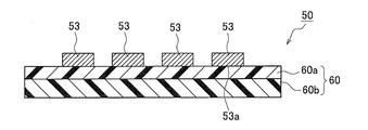
- a stacked body 50 in which a semiconductor chip 53 is temporarily fixed on a temporary fixing material 60 is prepared (Step A).
- the laminated body 50 is obtained, for example, by the following temporary fixing material preparation step and semiconductor chip temporary fixing step.
- a temporary fixing material 60 in which a thermally expandable pressure-sensitive adhesive layer 60a is laminated on a support base material 60b is prepared (see FIG. 2). In addition, it can replace with a thermally expansible adhesive layer, and can also use a radiation curing type adhesive layer.
- a temporary fixing material 60 including a thermally expandable pressure-sensitive adhesive layer will be described.
- the temporary fixing material in which the heat-expandable pressure-sensitive adhesive layer is laminated on the support base material is described in detail in Japanese Patent Application Laid-Open No. 2014-015490, etc., and will be briefly described below. .
- the thermally expandable pressure-sensitive adhesive layer 60a can be formed of a pressure-sensitive adhesive composition containing a polymer component and a foaming agent.
- a polymer component particularly the base polymer
- an acrylic polymer sometimes referred to as “acrylic polymer A”
- acrylic polymer A examples include those using (meth) acrylic acid ester as a main monomer component.
- Examples of the (meth) acrylic acid ester include (meth) acrylic acid alkyl esters (for example, methyl ester, ethyl ester, propyl ester, isopropyl ester, butyl ester, isobutyl ester, sec-butyl ester, t-butyl ester, Pentyl ester, isopentyl ester, hexyl ester, heptyl ester, octyl ester, 2-ethylhexyl ester, isooctyl ester, nonyl ester, decyl ester, isodecyl ester, undecyl ester, dodecyl ester, tridecyl ester, tetradecyl ester, Linear or branched alkyl ester having 1 to 30 carbon atoms, particularly 4 to 18 carbon atoms, of an alkyl group such as hexadecyl ester, oct
- the acrylic polymer A corresponds to other monomer components that can be copolymerized with the (meth) acrylic acid ester, if necessary, for the purpose of modifying cohesive strength, heat resistance, crosslinkability, and the like. Units may be included.
- the weight average molecular weight of the acrylic polymer A is not particularly limited, but is preferably 350,000 to 1,000,000, more preferably about 450,000 to 800,000.
- the heat-expandable pressure-sensitive adhesive layer 60a contains a foaming agent for imparting heat-expandability. Therefore, with the sealing body 58 formed on the thermally expandable pressure-sensitive adhesive layer 60a of the temporary fixing material 60 (see FIG. 6), the temporary fixing material 60 is at least partially heated at any time, and the heating is performed.
- the heat-expandable pressure-sensitive adhesive layer 60a is at least partially expanded, and this heat-expandable pressure-sensitive adhesive layer Due to at least partial expansion of 60a, the pressure-sensitive adhesive surface (interface with the sealing body 58) corresponding to the expanded portion is deformed into an uneven shape, and the thermally expandable pressure-sensitive adhesive layer 60a and the sealing body 58 are deformed.
- the adhesion area is reduced, whereby the adhesion force between the two is reduced, and the sealing body 58 can be peeled from the temporary fixing material 60 (see FIG. 7).
- the foaming agent used in the heat-expandable pressure-sensitive adhesive layer 60a is not particularly limited, and can be appropriately selected from known foaming agents.
- a foaming agent can be used individually or in combination of 2 or more types.
- thermally expandable microspheres can be suitably used.
- the heat-expandable microsphere is not particularly limited, and can be appropriately selected from known heat-expandable microspheres (such as various inorganic heat-expandable microspheres and organic heat-expandable microspheres).
- a microencapsulated foaming agent can be suitably used from the viewpoint of easy mixing operation.
- thermally expandable microspheres include microspheres in which substances such as isobutane, propane, and pentane that are easily gasified and expanded by heating are encapsulated in an elastic shell.
- the shell is often formed of a hot-melt material or a material that is destroyed by thermal expansion.
- Examples of the substance forming the shell include vinylidene chloride-acrylonitrile copolymer, polyvinyl alcohol, polyvinyl butyral, polymethyl methacrylate, polyacrylonitrile, polyvinylidene chloride, and polysulfone.
- the thickness of the heat-expandable pressure-sensitive adhesive layer is not particularly limited, and can be appropriately selected depending on the reduction in adhesive strength, and is, for example, about 5 ⁇ m to 300 ⁇ m (preferably 20 ⁇ m to 150 ⁇ m).
- the thermally expandable pressure-sensitive adhesive layer may be either a single layer or multiple layers.
- the heat-expandable pressure-sensitive adhesive layer has various additives (for example, a colorant, a thickener, a bulking agent, a filler, a tackifier, a plasticizer, an anti-aging agent, an antioxidant, and a surfactant. Agent, cross-linking agent, etc.).
- additives for example, a colorant, a thickener, a bulking agent, a filler, a tackifier, a plasticizer, an anti-aging agent, an antioxidant, and a surfactant. Agent, cross-linking agent, etc.).
- the support base material 60 b is a thin plate member that serves as a strength matrix of the temporary fixing material 60. What is necessary is just to select suitably considering the handleability, heat resistance, etc. as a material of the support base material 60b, for example, plastic materials, such as metal materials, such as SUS, polyimide, polyamide imide, polyether ether ketone, polyether sulfone, Glass, a silicon wafer, or the like can be used. Among these, a SUS plate is preferable from the viewpoints of heat resistance, strength, reusability, and the like.
- the thickness of the support substrate 60b can be appropriately selected in consideration of the intended strength and handleability, and is preferably 100 to 5000 ⁇ m, more preferably 300 to 2000 ⁇ m.
- the temporary fixing material 60 is obtained by forming the thermally expandable pressure-sensitive adhesive layer 60a on the support base material 60b.
- the heat-expandable pressure-sensitive adhesive layer is formed into a sheet-like layer by mixing, for example, a pressure-sensitive adhesive, a foaming agent (such as heat-expandable microspheres), and a solvent or other additives as necessary. It can be formed using conventional methods.
- the heat-expandable pressure-sensitive adhesive layer is formed by, for example, a method of applying the mixture on a release paper or the like to form a heat-expandable pressure-sensitive adhesive layer and transferring (transferring) the mixture onto the support substrate 60b. be able to.
- the thermally expandable pressure-sensitive adhesive layer can be thermally expanded by heating.
- an appropriate heating means such as a hot plate, a hot air dryer, a near infrared lamp, an air dryer or the like can be used.
- the heating temperature during the heat treatment may be equal to or higher than the foaming start temperature (thermal expansion start temperature) of the foaming agent (thermally expansible microspheres, etc.) in the heat-expandable pressure-sensitive adhesive layer.
- Typical heat treatment conditions are a temperature of 100 ° C. to 250 ° C., and a time of 1 second to 90 seconds (hot plate or the like) or 5 minutes to 15 minutes (hot air dryer or the like). Note that the heat treatment can be performed at an appropriate stage depending on the purpose of use. In some cases, an infrared lamp or heated water can be used as the heat source during the heat treatment.
- a plurality of semiconductor chips 53 are arranged on the prepared temporary fixing material 60 so that the circuit forming surface 53a faces the temporary fixing material 60 and temporarily fixed (see FIG. 2).
- a known device such as a flip chip bonder or a die bonder can be used for temporarily fixing the semiconductor chip 53.
- the layout and the number of arrangement of the semiconductor chips 53 can be appropriately set according to the shape and size of the temporary fixing material 60, the number of target packages produced, and the like. Can be arranged in a line. Although it does not specifically limit as a shape and size in planar view of the laminated body 50 (temporary fixing material 60), It can be made the same as the sealing sheet 10 with a separator. Heretofore, an example of the laminate preparation process has been shown.
- Step of preparing a sealing sheet with a double-sided separator Moreover, in the manufacturing method of the semiconductor device which concerns on this embodiment, the sheet
- Step of lifting sealing sheet with double-sided separator After the process B, as shown in FIG. 3, the double-sided separator-equipped sheet 10 is lifted by the adsorption collet 19 through the separator 41a. It should be noted that the interface between the separator 41a and the sealing sheet 11 of the sealing sheet with double-sided separator 10 and the interface between the sealing sheet 11 and the separator 41b are attached with a peeling force that does not peel off due to their own weight. Yes.
- the sealing sheet 40 is bent and adsorbed because the product ⁇ of the thickness t [mm] and the storage elastic modulus G ′ [Pa] at 50 ° C. satisfies the above formula 1. It can suppress that a clearance gap is made between the collet 19 and the sealing sheet 10 with a double-sided separator. As a result, the sealing sheet 10 with a double-sided separator is prevented from falling from the adsorption collet 19.
- Step of separating the separator from the sealing sheet with a double-sided separator Next, the separator 41b is peeled from the sealing sheet 10 with a double-sided separator. Note that the peeling force at the interface between the separator 41a and the sealing sheet 40 of the sealing sheet 10 with a double-sided separator is attached with a peeling force that does not peel when the separator 41b is peeled off.
- the stacked body 50 is disposed on the lower heating plate 62 with the surface on which the semiconductor chip 53 is temporarily fixed facing upward, and the semiconductor chip 53 of the stacked body 50 is temporarily fixed.
- seat 40 for sealing with the separator 41a is arrange
- the laminated body 50 may be first disposed on the lower heating plate 62, and then the sealing sheet 40 with the separator 41 a may be disposed on the laminated body 50, and the separator 41 a may be disposed on the laminated body 50.
- the attached sealing sheet 40 may be laminated first, and then a laminate in which the laminated body 50 and the sealing sheet 40 with the separator 41 a are laminated may be disposed on the lower heating plate 62.
- Step D heat pressing is performed by the lower heating plate 62 and the upper heating plate 64 so that the semiconductor chip 53 is embedded in the sealing sheet 40, and the semiconductor chip 53 is embedded in the sealing sheet 40.
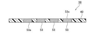
- the sealed body 58 is formed (step D).
- the sealing sheet 40 functions as a sealing resin for protecting the semiconductor chip 53 and its accompanying elements from the external environment. Thereby, the sealing body 58 in which the semiconductor chip 53 temporarily fixed on the temporary fixing material 60 is embedded in the sealing sheet 40 is obtained.
- the temperature is preferably 40 to 150 ° C., more preferably 60 to 120 ° C., and the pressure is, for example, 0.
- the pressure is 1 to 10 MPa, preferably 0.5 to 8 MPa, and the time is, for example, 0.3 to 10 minutes, preferably 0.5 to 5 minutes.
- Examples of the hot pressing method include a parallel plate press and a roll press. Of these, a parallel plate press is preferable.
- the pressure reducing conditions the pressure is, for example, 0.1 to 5 kPa, preferably 0.1 to 100 Pa, and the reduced pressure holding time (the time from the start of pressure reduction to the start of pressing) is, for example, 5 to 600 seconds. Yes, preferably 10 to 300 seconds.
- the sealing sheet 40 is thermally cured. Specifically, for example, the entire sealing body 58 in which the semiconductor chip 53 temporarily fixed on the temporary fixing material 60 is embedded in the sealing sheet 40 is heated.
- the heating temperature is preferably 100 ° C or higher, more preferably 120 ° C or higher.
- the upper limit of the heating temperature is preferably 200 ° C. or lower, more preferably 180 ° C. or lower.
- the heating time is preferably 10 minutes or more, more preferably 30 minutes or more.
- the upper limit of the heating time is preferably 180 minutes or less, more preferably 120 minutes or less.
- you may pressurize as needed Preferably it is 0.1 Mpa or more, More preferably, it is 0.5 Mpa or more.
- the upper limit is preferably 10 MPa or less, more preferably 5 MPa or less.
- the temporary fixing material 60 is heated to thermally expand the thermally expandable pressure-sensitive adhesive layer 60 a, thereby peeling between the thermally expandable pressure-sensitive adhesive layer 60 a and the sealing body 58.
- a procedure in which peeling is performed at the interface between the support base 60b and the thermally expandable pressure-sensitive adhesive layer 60a and then peeling is performed by thermal expansion at the interface between the thermally expandable pressure-sensitive adhesive layer 60a and the sealing body 58 is also suitable. Can be adopted.
- the heat-expandable pressure-sensitive adhesive layer 60a is heated and thermally expanded to reduce the adhesive force, thereby easily peeling at the interface between the heat-expandable pressure-sensitive adhesive layer 60a and the sealing body 58. Can be done.
- the conditions for thermal expansion the conditions in the above-mentioned column “Thermal expansion method for thermally expandable pressure-sensitive adhesive layer” can be preferably employed.
- the heat-expandable pressure-sensitive adhesive layer has a structure that does not peel off by heating in the thermosetting step but peels off by heating in the heat-expandable pressure-sensitive adhesive layer peeling step.
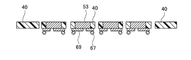
- the sealing sheet 40 of the sealing body 58 is ground to expose the back surface 53 c of the semiconductor chip 53.
- the method for grinding the sealing sheet 40 is not particularly limited, and examples thereof include a grinding method using a grindstone that rotates at high speed.
- a rewiring 69 connected to the exposed semiconductor chip 53 is formed on the sealing body 58 (see FIG. 9).
- a metal seed layer is formed on the exposed semiconductor chip 53 by using a known method such as a vacuum film forming method, and the rewiring is performed by a known method such as a semi-additive method.
- Wiring 69 can be formed.
- an insulating layer such as polyimide or PBO may be formed on the rewiring 69 and the sealing body 58.
- bumping processing for forming bumps 67 on the formed rewiring 69 may be performed (see FIG. 9).
- the bumping process can be performed by a known method such as a solder ball or solder plating.
- the “laminate” of the present invention is the “laminate 50 in which the semiconductor chip 53 is temporarily fixed on the temporary fixing material 60”
- the “laminate” in the present invention is not limited to this example, and any semiconductor chip may be fixed to a support having a certain degree of strength. That is, the “laminate” may be “a laminate in which a semiconductor chip is fixed on a support”.
- Other examples of the “laminated body” in the present invention include, for example, “a laminated body in which a semiconductor chip is flip-chip bonded to a circuit forming surface of a semiconductor wafer” (so-called chip-on-wafer), and “a semiconductor chip is an organic substrate. Can be mentioned.
- Epoxy resin YSLV-80XY manufactured by Nippon Steel Chemical Co., Ltd. (bisphenol F type epoxy resin, epkin equivalent 200 g / ep. Softening point 80 ° C.)
- Phenolic resin MEH-7851-SS (phenol resin having a biphenylaralkyl skeleton, hydroxyl group equivalent 203 g / eq. Softening point 67 ° C.) manufactured by Meiwa Kasei Co., Ltd.
- Silane coupling agent KBM-403 (3-glycidoxypropyltrimethoxysilane) manufactured by Shin-Etsu Chemical Co., Ltd.
- Curing accelerator 2PHZ-PW (2-phenyl-4,5-dihydroxymethylimidazole) manufactured by Shikoku Kasei Kogyo Co., Ltd.
- Thermoplastic resin J-5800 manufactured by Mitsubishi Rayon Co., Ltd. (acrylic rubber-based stress relaxation agent)
- Filler FB-9454FC manufactured by Denki Kagaku Kogyo Co., Ltd. (fused spherical silica powder, average particle size 17.6 ⁇ m)
- Carbon black # 20 (particle size 50 nm) manufactured by Mitsubishi Chemical Corporation
- sealing sheet (Examples 1 to 12, Comparative Examples 1 to 8) According to the blending ratio shown in Table 1, each component is blended and melt-kneaded in a roll kneader at 60 to 120 ° C. for 10 minutes under reduced pressure conditions (0.01 kg / cm 2 ). Kneaded materials (resin compositions A to E) were prepared. Next, the obtained resin composition was formed into a sheet shape by a flat plate pressing method. Table 2 shows combinations of resin composition types, sheet thicknesses, and areas. Thus, sealing sheets according to Examples 1 to 12 and Comparative Examples 1 to 8 were obtained. In this embodiment, the area 250,000 mm 2 is 500 mm long ⁇ 500 mm wide, and the area 40000 mm 2 is 200 mm long ⁇ 200 mm wide.
- sealing sheet with double-sided separator MRU-50 (Mitsubishi Resin Co., Ltd. silicone-removed MRU-50 (corresponding to the separator of the present invention, thickness 50 ⁇ m)) was pasted on both surfaces of each sealing sheet produced above.
- sealing sheets with double-sided separators according to Examples 1 to 12 and Comparative Examples 1 to 8 were obtained.
- a glass plate having a length of 200 mm, a width of 200 mm, and a thickness of 1.1 mm was prepared.
- a temporary fixing material (REVALPHA No. 3195V manufactured by Nitto Denko Corporation) was pasted on this glass plate with a laminator.
- chips of length 7 mm ⁇ width 7 mm ⁇ thickness 0.4 mm were arranged in a matrix of 13 ⁇ length ⁇ 13 width.
- the chip mounting interval (interval between the end of the chip and the end of the chip) was 16 mm.
- a sealing sheet formed into a sheet having a thickness of 0.6 mm was laminated on the glass carrier and hot-pressed using a vacuum press apparatus (device name: VACUUM ACE, manufactured by Mikado Technos). Next, trimming was performed to remove unnecessary resin on a 60 ° C. hot plate. Thereafter, heat treatment was performed at 150 ° C. for 1 hour to cure the resin. Then, the temporary fix
- Microscope observation (device name: VHX-2000, manufactured by Keyence Corporation) of the boundary between the chip and the resin on the chip exposed surface of the obtained sealing body, and observation of unfilled area or air entrapment traces at the end of the chip The case where it was made was evaluated as embeddability x and the case where it was not observed was evaluated as embeddability ⁇ . The results are shown in Table 2.
Priority Applications (4)
| Application Number | Priority Date | Filing Date | Title |
|---|---|---|---|
| EP15836357.2A EP3187561B1 (en) | 2014-08-29 | 2015-08-06 | Sealing sheet with a separator and production method for semiconductor device |
| SG11201701445PA SG11201701445PA (en) | 2014-08-29 | 2015-08-06 | Sealing sheet, sealing sheet with separator, semiconductor device, and production method for semiconductor device |
| US15/506,884 US20170278716A1 (en) | 2014-08-29 | 2015-08-06 | Sealing sheet, sealing sheet with separator, semiconductor device, and production method for semiconductor device |
| CN201580046113.8A CN106795418B (zh) | 2014-08-29 | 2015-08-06 | 密封用片、带隔片的密封用片、半导体装置、及半导体装置的制造方法 |
Applications Claiming Priority (2)
| Application Number | Priority Date | Filing Date | Title |
|---|---|---|---|
| JP2014-175772 | 2014-08-29 | ||
| JP2014175772A JP6313165B2 (ja) | 2014-08-29 | 2014-08-29 | 熱硬化性の封止用樹脂シート、セパレータ付き封止用シート、半導体装置、及び、半導体装置の製造方法 |
Publications (1)
| Publication Number | Publication Date |
|---|---|
| WO2016031521A1 true WO2016031521A1 (ja) | 2016-03-03 |
Family
ID=55399420
Family Applications (1)
| Application Number | Title | Priority Date | Filing Date |
|---|---|---|---|
| PCT/JP2015/072379 WO2016031521A1 (ja) | 2014-08-29 | 2015-08-06 | 封止用シート、セパレータ付き封止用シート、半導体装置、及び、半導体装置の製造方法 |
Country Status (7)
| Country | Link |
|---|---|
| US (1) | US20170278716A1 (zh) |
| EP (1) | EP3187561B1 (zh) |
| JP (1) | JP6313165B2 (zh) |
| CN (2) | CN110600434A (zh) |
| SG (1) | SG11201701445PA (zh) |
| TW (1) | TWI709642B (zh) |
| WO (1) | WO2016031521A1 (zh) |
Cited By (2)
| Publication number | Priority date | Publication date | Assignee | Title |
|---|---|---|---|---|
| CN113517205A (zh) * | 2020-04-27 | 2021-10-19 | 台湾积体电路制造股份有限公司 | 半导体器件及其形成方法 |
| US11942436B2 (en) | 2020-04-27 | 2024-03-26 | Taiwan Semiconductor Manufacturing Company, Ltd. | Passivation scheme design for wafer singulation |
Families Citing this family (5)
| Publication number | Priority date | Publication date | Assignee | Title |
|---|---|---|---|---|
| US11495571B2 (en) * | 2016-08-24 | 2022-11-08 | Toray Engineering Co., Ltd. | Mounting method and mounting device |
| US10522499B2 (en) * | 2017-02-09 | 2019-12-31 | Invensas Bonding Technologies, Inc. | Bonded structures |
| CN109686854A (zh) * | 2017-10-19 | 2019-04-26 | 京东方科技集团股份有限公司 | 封装结构及封装方法、电子装置及封装薄膜回收方法 |
| DE102018103149B4 (de) | 2017-11-15 | 2024-03-07 | Taiwan Semiconductor Manufacturing Co., Ltd. | Finnen integrierter Schaltungsvorrichtungen und zugehöriges Herstellungsverfahren |
| EP3873182A4 (en) * | 2018-10-22 | 2023-01-25 | Toyobo Co., Ltd. | METHOD OF MAKING DEVICE CONNECTED BODY AND DEVICE CONNECTED BODY |
Citations (2)
| Publication number | Priority date | Publication date | Assignee | Title |
|---|---|---|---|---|
| JP2008311348A (ja) * | 2007-06-13 | 2008-12-25 | Nitto Denko Corp | 熱硬化型接着シート |
| JP2014131016A (ja) * | 2012-11-29 | 2014-07-10 | Nitto Denko Corp | 熱硬化性樹脂シート及び電子部品パッケージの製造方法 |
Family Cites Families (6)
| Publication number | Priority date | Publication date | Assignee | Title |
|---|---|---|---|---|
| WO2005056676A1 (ja) * | 2003-12-11 | 2005-06-23 | Hitachi Chemical Co., Ltd. | 封止用エポキシ樹脂成形材料および電子部品装置 |
| JP5309886B2 (ja) * | 2007-10-22 | 2013-10-09 | 日立化成株式会社 | 半導体封止用フィルム状接着剤、半導体装置の製造方法及び半導体装置 |
| US8484759B2 (en) * | 2009-08-17 | 2013-07-09 | Ut-Battelle, Llc | Spatially resolved quantitative mapping of thermomechanical properties and phase transition temperatures using scanning probe microscopy |
| EP2559746A4 (en) * | 2010-04-13 | 2013-09-18 | Mitsubishi Plastics Inc | CLEAR DOUBLE-SIDED ADHESIVE SHEET |
| JP2012241063A (ja) * | 2011-05-17 | 2012-12-10 | Nitto Denko Corp | 半導体装置製造用の接着シート |
| JP2013074184A (ja) * | 2011-09-28 | 2013-04-22 | Nitto Denko Corp | 半導体装置の製造方法 |
-
2014
- 2014-08-29 JP JP2014175772A patent/JP6313165B2/ja active Active
-
2015
- 2015-08-06 SG SG11201701445PA patent/SG11201701445PA/en unknown
- 2015-08-06 CN CN201910870833.6A patent/CN110600434A/zh active Pending
- 2015-08-06 US US15/506,884 patent/US20170278716A1/en not_active Abandoned
- 2015-08-06 EP EP15836357.2A patent/EP3187561B1/en active Active
- 2015-08-06 WO PCT/JP2015/072379 patent/WO2016031521A1/ja active Application Filing
- 2015-08-06 CN CN201580046113.8A patent/CN106795418B/zh active Active
- 2015-08-26 TW TW104127979A patent/TWI709642B/zh active
Patent Citations (2)
| Publication number | Priority date | Publication date | Assignee | Title |
|---|---|---|---|---|
| JP2008311348A (ja) * | 2007-06-13 | 2008-12-25 | Nitto Denko Corp | 熱硬化型接着シート |
| JP2014131016A (ja) * | 2012-11-29 | 2014-07-10 | Nitto Denko Corp | 熱硬化性樹脂シート及び電子部品パッケージの製造方法 |
Non-Patent Citations (1)
| Title |
|---|
| See also references of EP3187561A4 * |
Cited By (2)
| Publication number | Priority date | Publication date | Assignee | Title |
|---|---|---|---|---|
| CN113517205A (zh) * | 2020-04-27 | 2021-10-19 | 台湾积体电路制造股份有限公司 | 半导体器件及其形成方法 |
| US11942436B2 (en) | 2020-04-27 | 2024-03-26 | Taiwan Semiconductor Manufacturing Company, Ltd. | Passivation scheme design for wafer singulation |
Also Published As
| Publication number | Publication date |
|---|---|
| TWI709642B (zh) | 2020-11-11 |
| CN110600434A (zh) | 2019-12-20 |
| CN106795418A (zh) | 2017-05-31 |
| JP2016050240A (ja) | 2016-04-11 |
| EP3187561A4 (en) | 2017-09-20 |
| JP6313165B2 (ja) | 2018-04-18 |
| EP3187561A1 (en) | 2017-07-05 |
| TW201619341A (zh) | 2016-06-01 |
| US20170278716A1 (en) | 2017-09-28 |
| EP3187561B1 (en) | 2019-10-09 |
| CN106795418B (zh) | 2019-10-15 |
| SG11201701445PA (en) | 2017-03-30 |
Similar Documents
| Publication | Publication Date | Title |
|---|---|---|
| JP6313165B2 (ja) | 熱硬化性の封止用樹脂シート、セパレータ付き封止用シート、半導体装置、及び、半導体装置の製造方法 | |
| JP5961055B2 (ja) | 封止樹脂シート、電子部品パッケージの製造方法及び電子部品パッケージ | |
| US9382455B2 (en) | Adhesive composition, an adhesive sheet and a production method of a semiconductor device | |
| US9434865B2 (en) | Adhesive composition, an adhesive sheet and a production method of a semiconductor device | |
| TWI616476B (zh) | Thermosetting resin sheet and method of manufacturing electronic component package | |
| JP6484061B2 (ja) | 電子部品パッケージの製造方法 | |
| TW201205660A (en) | Film for flip chip type semiconductor back surface, and dicing tape-integrated film for semiconductor back surface | |
| WO2015025661A1 (ja) | 封止用シート、及び、半導体装置の製造方法 | |
| WO2015015979A1 (ja) | 半導体装置の製造方法、及び、封止用シート | |
| TW201513195A (zh) | 半導體封裝件之製造方法 | |
| US20170040287A1 (en) | Electronic component device production method and electronic component sealing sheet | |
| US10128131B2 (en) | Sealing sheet with separators on both surfaces, and method for manufacturing semiconductor device | |
| WO2016080116A1 (ja) | 半導体装置の製造方法 | |
| WO2016117268A1 (ja) | 封止用シート | |
| JP6302801B2 (ja) | 封止用シート | |
| WO2015015980A1 (ja) | 半導体装置の製造方法 | |
| JP6677966B2 (ja) | セパレータ付き封止用シート、及び、半導体装置の製造方法 | |
| JP6630861B2 (ja) | セパレータ付き封止用シート、及び、半導体装置の製造方法 | |
| WO2015053081A1 (ja) | 半導体装置の製造方法 |
Legal Events
| Date | Code | Title | Description |
|---|---|---|---|
| 121 | Ep: the epo has been informed by wipo that ep was designated in this application |
Ref document number: 15836357 Country of ref document: EP Kind code of ref document: A1 |
|
| WWE | Wipo information: entry into national phase |
Ref document number: 15506884 Country of ref document: US |
|
| NENP | Non-entry into the national phase |
Ref country code: DE |
|
| REEP | Request for entry into the european phase |
Ref document number: 2015836357 Country of ref document: EP |
|
| WWE | Wipo information: entry into national phase |
Ref document number: 2015836357 Country of ref document: EP |