WO2016017443A1 - 光導波路およびそれを用いた位置センサ - Google Patents
光導波路およびそれを用いた位置センサ Download PDFInfo
- Publication number
- WO2016017443A1 WO2016017443A1 PCT/JP2015/070473 JP2015070473W WO2016017443A1 WO 2016017443 A1 WO2016017443 A1 WO 2016017443A1 JP 2015070473 W JP2015070473 W JP 2015070473W WO 2016017443 A1 WO2016017443 A1 WO 2016017443A1
- Authority
- WO
- WIPO (PCT)
- Prior art keywords
- core
- divided
- cores
- width
- lattice
- Prior art date
- Legal status (The legal status is an assumption and is not a legal conclusion. Google has not performed a legal analysis and makes no representation as to the accuracy of the status listed.)
- Ceased
Links
Images





Classifications
-
- G—PHYSICS
- G06—COMPUTING OR CALCULATING; COUNTING
- G06F—ELECTRIC DIGITAL DATA PROCESSING
- G06F3/00—Input arrangements for transferring data to be processed into a form capable of being handled by the computer; Output arrangements for transferring data from processing unit to output unit, e.g. interface arrangements
- G06F3/01—Input arrangements or combined input and output arrangements for interaction between user and computer
- G06F3/03—Arrangements for converting the position or the displacement of a member into a coded form
- G06F3/041—Digitisers, e.g. for touch screens or touch pads, characterised by the transducing means
- G06F3/042—Digitisers, e.g. for touch screens or touch pads, characterised by the transducing means by opto-electronic means
- G06F3/0421—Digitisers, e.g. for touch screens or touch pads, characterised by the transducing means by opto-electronic means by interrupting or reflecting a light beam, e.g. optical touch-screen
-
- G—PHYSICS
- G01—MEASURING; TESTING
- G01B—MEASURING LENGTH, THICKNESS OR SIMILAR LINEAR DIMENSIONS; MEASURING ANGLES; MEASURING AREAS; MEASURING IRREGULARITIES OF SURFACES OR CONTOURS
- G01B11/00—Measuring arrangements characterised by the use of optical techniques
-
- G—PHYSICS
- G01—MEASURING; TESTING
- G01L—MEASURING FORCE, STRESS, TORQUE, WORK, MECHANICAL POWER, MECHANICAL EFFICIENCY, OR FLUID PRESSURE
- G01L1/00—Measuring force or stress, in general
- G01L1/24—Measuring force or stress, in general by measuring variations of optical properties of material when it is stressed, e.g. by photoelastic stress analysis using infrared, visible light, ultraviolet
- G01L1/242—Measuring force or stress, in general by measuring variations of optical properties of material when it is stressed, e.g. by photoelastic stress analysis using infrared, visible light, ultraviolet the material being an optical fibre
- G01L1/243—Measuring force or stress, in general by measuring variations of optical properties of material when it is stressed, e.g. by photoelastic stress analysis using infrared, visible light, ultraviolet the material being an optical fibre using means for applying force perpendicular to the fibre axis
-
- G—PHYSICS
- G02—OPTICS
- G02B—OPTICAL ELEMENTS, SYSTEMS OR APPARATUS
- G02B6/00—Light guides; Structural details of arrangements comprising light guides and other optical elements, e.g. couplings
- G02B6/10—Light guides; Structural details of arrangements comprising light guides and other optical elements, e.g. couplings of the optical waveguide type
- G02B6/12—Light guides; Structural details of arrangements comprising light guides and other optical elements, e.g. couplings of the optical waveguide type of the integrated circuit kind
- G02B6/122—Basic optical elements, e.g. light-guiding paths
- G02B6/125—Bends, branchings or intersections
-
- G—PHYSICS
- G06—COMPUTING OR CALCULATING; COUNTING
- G06F—ELECTRIC DIGITAL DATA PROCESSING
- G06F3/00—Input arrangements for transferring data to be processed into a form capable of being handled by the computer; Output arrangements for transferring data from processing unit to output unit, e.g. interface arrangements
- G06F3/01—Input arrangements or combined input and output arrangements for interaction between user and computer
- G06F3/03—Arrangements for converting the position or the displacement of a member into a coded form
- G06F3/041—Digitisers, e.g. for touch screens or touch pads, characterised by the transducing means
- G06F3/042—Digitisers, e.g. for touch screens or touch pads, characterised by the transducing means by opto-electronic means
Definitions
- the present invention relates to an optical waveguide and a position sensor using the optical waveguide to optically detect a pressed position.
- the present applicant has proposed a position sensor that optically detects the pressed position (see, for example, Patent Document 1).
- a plurality of linear cores serving as optical paths are formed in a lattice shape, and the lattice-shaped core is sandwiched between two sheet-shaped clad layers, and the lattice-shaped core is connected to the lattice-shaped core.
- a light emitting element for propagating light and a light receiving element for receiving the propagated light are provided.
- the surface portion of the position sensor itself corresponding to the lattice-shaped core is pressed with a pen tip or the like, the core of the pressed portion is deformed, and light is detected by the light receiving element from the core of the pressed portion. Since the level is lowered, the pressing position can be detected.
- the intersection part of the lattice-shaped core is a continuous intersection in which the cores 12 are continuous.
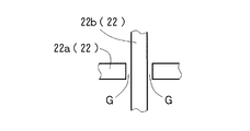
- the discontinuous intersection is a state in which one core (lateral core in FIG. 8) 22a of two intersecting cores 22 is divided by the other core (vertical core in FIG. 8) 22b. Gap G is formed between the other divided core 22b and the divided end of one divided core 22a. Then, since light leaking from the gap G is generated in one of the divided cores 22a, the crossing loss in the one divided core 22a is increased, but the other divided core 22b is also divided. The crossing loss is 0 (zero) because the linear core 22 has no continuous crossing points. Therefore, when the crossing losses in the intersecting cores 22a and 22b in the two directions are totaled, the crossing loss is reduced.
- the crossing loss in the other divided core is 0 (zero) even in the position sensor.
- Crossing loss at the core increases. Therefore, it is desirable to further reduce the crossing loss in one of the divided cores and further reduce the total crossing loss in the two intersecting directions.
- the present invention has been made in view of such circumstances, and in the lattice-like core, the crossing portion of the core is in a state where one of the intersecting cores is divided by the other core.
- An optical waveguide in which a crossing loss is further reduced when a gap is formed between the divided core and an end portion of the divided core, and a position sensor using the same The purpose is to provide
- the present invention provides a sheet-shaped light guide including a plurality of linear cores formed in a lattice shape and two sheet-shaped clad layers that sandwich the lattice-shaped core.
- a waveguide in which one of the two-direction cores intersecting at the lattice-shaped intersection is divided by the other core, and the other divided core and one divided core
- An optical waveguide in which a gap is formed between each of the split-side end portions, and the width of the split-side end portion of one of the split cores is set to be greater than the width of the other split core. This is the first gist.
- the present invention also provides a sheet-like optical waveguide in which a plurality of linear cores formed in a lattice shape are sandwiched between two sheet-like clad layers, and a light-emitting element connected to one end face of the core.
- a position sensor comprising a light receiving element connected to the other end surface of the core, wherein one of the two-direction cores intersecting at the lattice-like intersection is divided by the other core
- a gap is formed between the divided core and the split-side end of the split core, and the width of the split-side end of the split core is
- the light is emitted from the light emitting element through the core of the optical waveguide, and is received by the light receiving element, corresponding to the lattice-shaped core portion.
- the surface area of itself is taken as the input area,
- the pressing position in the force area, the second aspect of the position sensor to identify by light propagation quantity of the core that has changed by the pressing.
- the present inventors are in a state in which one of the intersecting cores is divided by the other core, and the other core is divided.
- the widths of the two intersecting cores were the same, but when the width of one divided core was set larger than the width of the other divided core, The present inventors have found that the crossing loss in the core can be further reduced, and have reached the present invention.
- the width of one divided core is set larger than the width of the other divided core as in the present invention, the width of the other divided core becomes relatively narrow. For this reason, in one of the divided cores, the length of the divided portion is shortened. Therefore, the probability that light leaks from the divided portion is reduced, and the cross loss is reduced.
- the other core that is divided is a linear core that has neither a divided point nor a continuous crossing point, and therefore the crossing loss is 0 (zero).
- the optical waveguide of the present invention has a lattice-shaped core, and one of the two-direction cores intersecting at the intersection is in a state of being divided by the other core, A gap is formed between each of the divided cores and the end of the divided core, and the width of the divided end of the one core is larger than the width of the other divided core. Is set. As a result, the number of times the light is reflected on the side wall (the number of times it hits the side wall) is reduced in one of the divided cores, and the length of the divided part is shortened, so that the probability of light leaking from the divided part is reduced. Crossing loss has been reduced.
- the optical waveguide of the present invention can further reduce the crossing loss in the lattice-like core by summing up the crossing loss in the two intersecting cores.
- the position sensor of this invention is equipped with the optical waveguide of the said invention, the crossing loss in a grid
- the width of the end portion of one of the divided cores is set to 50 times or less the width of the other divided core, the width of the core is more appropriate for the position sensor. Can be set to any value.
- (A) is a top view which shows typically one embodiment of the position sensor of the present invention
- (b) is an enlarged view schematically showing an enlarged intersection of lattice-like cores in the position sensor. It is a top view.
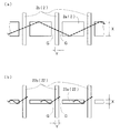
- It is explanatory drawing which shows typically the propagation method of the light in the divided
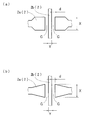
- (A) is an enlarged plan view which shows typically the modification of the cross
- FIG. 1A is a plan view showing an embodiment of the position sensor of the present invention.
- the position sensor of this embodiment includes a rectangular sheet-shaped optical waveguide W having a lattice-shaped core 2, and a light-emitting element 4 connected to one end face of the linear core 2 constituting the lattice-shaped core 2. And a light receiving element 5 connected to the other end face of the linear core 2.
- the light emitted from the light emitting element 4 passes through the core 2 and is received by the light receiving element 5.
- the core 2 is indicated by a chain line, and the thickness of the chain line indicates the thickness of the core 2.
- the number of cores 2 is omitted.
- the arrow of Fig.1 (a) has shown the direction where light travels.
- the optical waveguide W is an embodiment of the optical waveguide of the present invention, and each crossing portion of the lattice-like core 2 has two intersecting directions (horizontal) as shown in a plan view in FIG. 1a (the horizontal core in FIG. 1 (b)) 2a is divided by the other core (the vertical core in FIG. 1 (b)) 2b.
- a discontinuous intersection is formed in which a gap G is formed between the divided core 2b and the divided end of the divided core 2a.
- the width (X) of one divided core 2a is set to be larger than the width (Y) of the other divided core 2b [1 ⁇ (X / Y)]. This is one of the major features of the present invention.
- the intersecting two-direction cores 2a and 2b are set to have a constant width (X, Y).
- the width d of the gap G exceeds 0 (zero), and is usually set to 50 ⁇ m or less, preferably 20 ⁇ m or less.
- one of the intersecting cores 2a is divided by the other core 2b, and the other divided core 2b and an end of the divided one core 2a on the divided side
- the width (X) of one divided core 2a is larger than the width (Y) of the other divided core 2b at a discontinuous intersection with gaps G formed between them [1 ⁇ (X / Y) If set, the crossing loss in the lattice-like core 2 can be further reduced.
- FIG. 2 (a) in which the cores 2a and 2b are set as described above and the two-way cores 22a and 22b intersecting with each other as in the prior art (see FIG. 8) described above have the same width.
- FIG. 2B is set to the other divided core (the vertical cores in FIGS. 2A and 2B) 2b and 22b, and the width is the same.
- the probability is high, and the probability that light leaks to the side from the divided part is high (see the dashed line arrow in FIG. 2B). From this, the crossing loss in one of the divided cores 2a and 22a is smaller in FIG. 2A where the core width (X) is large.
- FIG. 3A in which the cores 2a and 2b are set as described above and the two-way cores 22a and 22b that intersect with each other as in the prior art (see FIG. 8) described above have the same width.
- 3B is compared with the divided one core [lateral cores in FIGS. 3A and 3B] 2a and 22a having the same width. ), Since the width (Y) of the other core 2b is small and the length L of the split portion is short, the probability of light leaking from the split portion is low [the arrow of the one-dot chain line in FIG. reference ⁇ . On the other hand, in FIG.
- the other core 2b that is divided is a straight core 2 that has neither a divided part nor a continuous crossing part, so that the crossing loss is 0 (zero).
- the sheet-like optical waveguide W has a lattice-like core 2 embedded in the surface portion of the sheet-like underclad layer 1, as shown in a sectional view in FIG.
- the surface of the under clad layer 1 and the top surface of the core 2 are formed flush with each other, and the sheet-like over clad layer 3 is formed in a state where the surface of the under clad layer 1 and the top surface of the core 2 are covered. It has become.
- the gap G at the part where the core 2 a is divided is formed of the material for forming the under cladding layer 1.
- the thickness of each layer is, for example, in the range of 10 to 500 ⁇ m for the under cladding layer 1, in the range of 5 to 100 ⁇ m for the core 2, and 1 to 1 for the over cladding layer 3. It is set within the range of 200 ⁇ m.
- the surface portion of the over clad layer 3 corresponding to the lattice-like core 2 portion is an input region.
- Input of characters or the like to the position sensor is performed by writing characters or the like in the input area directly or via a resin film or paper with an input body such as a pen.
- the input area is pressed with a pen tip or the like, the core 2 of the pressed portion is deformed, and the light propagation amount of the core 2 is reduced. For this reason, in the core 2 of the pressed portion, the detection level of light at the light receiving element 5 is lowered, so that the pressed position can be detected.
- the position sensor since the cross loss in the lattice-like core 2 is very small, the detection level of light in the light receiving element 5 does not decrease so much in the core 2 other than the pressed portion. Therefore, the difference in the light detection level at the light receiving element 5 increases between the pressed portion and other than the pressed portion, and the pressed position by the pen tip or the like can be clearly detected. In addition, even if the amount of decrease in the detection level due to the pressing is small due to a low writing pressure at the time of the input, a difference from the detection level other than the pressing portion clearly appears, and the pressing position is surely confirmed. Can be detected. Thus, the position sensor has high detection sensitivity of the pressed position.
- the portion of the core 2 connected to the light receiving element 5 needs to be formed with a reduced width in accordance with the dimensions of the light receiving element 5 so as to be connectable to the light receiving element 5. is there.
- a width reduction loss (light propagation loss due to core width reduction) occurs, and the width reduction loss increases as the core width reduction ratio increases.
- the width (X) of one divided core 2a is larger than the width (Y) of the other divided core 2b [1 ⁇ (X / Y)], and if the width (X) of one of the divided cores 2a is large, the cross loss is reduced, but the width reduction loss is increased.
- the width (X) of one divided core 2a is changed to the width (Y) of the other divided core 2b. It is preferable to set it to 50 times or less [1 ⁇ (X / Y) ⁇ 50].
- the elastic modulus of the core 2 is preferably set larger than the elastic modulus of the under cladding layer 1 and the over cladding layer 3. The reason is that if the elastic modulus is set in the opposite direction, the periphery of the core 2 becomes hard, so that the optical waveguide W having a considerably larger area than the area of the pen tip or the like that presses the input region portion of the over clad layer 3. This is because the above-mentioned portion is recessed and it is difficult to accurately detect the pressed position.
- each elastic modulus for example, the elastic modulus of the core 2 is set within a range of 1 GPa or more and 10 GPa or less, and the elastic modulus of the over clad layer 3 is set within a range of 0.1 GPa or more and less than 10 GPa
- the elastic modulus of the under cladding layer 1 is preferably set within a range of 0.1 MPa to 1 GPa.
- the elastic modulus of the core 2 is large, the core 2 is not crushed by a small pressing force (the cross-sectional area of the core 2 is not reduced), but the optical waveguide W is recessed by the pressing, and therefore corresponds to the recessed portion.
- Light leakage (scattering) occurs from the bent portion of the core 2, and the detection level of light at the light receiving element 5 (see FIG. 1) decreases in the core 2, so that the pressed position can be detected. .
- Examples of the material for forming the under cladding layer 1, the core 2 and the over cladding layer 3 include a photosensitive resin, a thermosetting resin, and the like, and the optical waveguide W can be manufactured by a manufacturing method corresponding to the forming material.
- the refractive index of the core 2 is set larger than the refractive indexes of the under cladding layer 1 and the over cladding layer 3.
- the elastic modulus and refractive index can be adjusted by, for example, selecting the type of each forming material and adjusting the composition ratio.
- a rubber sheet may be used as the undercladding layer 1 and the cores 2 may be formed in a lattice shape on the rubber sheet.
- the two intersecting cores 2a and 2b are set to have a constant width (X, Y).
- one of the divided cores is divided. 2a may not be a fixed width. That is, in FIG. 5 (a), an end portion on one side of the divided core 2a is set to a constant width (X), and the width (X) of the end portion of the other core 2b is divided. [1 ⁇ (X / Y)] is set larger than the width (Y), and the portion of the core 2a other than the end of the constant width (X) is set to a width smaller than the constant width (X). Has been. On the other hand, in FIG.
- the width (X) of the divided end face of one core 2a is larger than the width (Y) of the other divided core 2b [1 ⁇ (X / Y).
- the portion of the end portion of the core 2a other than the end face is set so that the width gradually decreases as the distance from the separated core 2b increases. Even in these cases, the crossing loss in the lattice-like core 2 can be further reduced as in the above-described embodiment.
- the cross-sectional structure of the optical waveguide W is as shown in FIG. 4, but may be other, for example, as shown in the cross-sectional view of FIG. 1 may be formed in a predetermined pattern in a state where the core 2 protrudes, and may have a structure in which the over cladding layer 3 is formed on the surface of the under cladding layer 1 in a state where the core 2 is covered. .
- the gap G at the part where the core 2 a is divided is formed of the material for forming the over clad layer 3.
- Component a 75 parts by weight of an epoxy resin (Mitsubishi Chemical Corporation, YL7410).
- Component b 25 parts by weight of an epoxy resin (manufactured by Mitsubishi Chemical Corporation, JER1007).
- Component c 2 parts by weight of a photoacid generator (manufactured by Sun Apro, CPI101A).
- Component d 75 parts by weight of an epoxy resin (manufactured by Daicel Corporation, EHPE3150).
- Component e 25 parts by weight of epoxy resin (KI-3000-4, manufactured by Tohto Kasei Co., Ltd.)
- Component f 1 part by weight of a photoacid generator (manufactured by ADEKA, SP170).
- Component g 50 parts by weight of ethyl lactate (manufactured by Wako Pure Chemical Industries, Ltd., solvent).
- a core forming material was prepared by mixing these components d to g.
- an over clad layer was formed on the surface of a glass substrate by spin coating using the above-mentioned over clad layer forming material.
- the thickness of this over clad layer was 25 ⁇ m.
- the elastic modulus was 3 MPa.
- the elastic modulus was measured using a viscoelasticity measuring device (TA instruments Japan Inc., RSA3).
- a lattice-like core was formed on the surface of the over clad layer by photolithography using the core forming material.
- the horizontal core is divided by the vertical core, and the vertical core and the horizontal core are separated from each other.
- a discontinuous intersection in which a gap was formed between each end portion was used (see FIG. 1B).
- Comparative Example 3 a continuous intersection in which the core was not divided (see FIG. 7) was used.
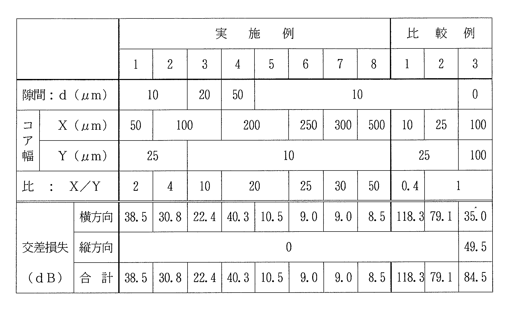
- the width (X) of the core in the horizontal direction, the width (Y) of the core in the vertical direction, and the width (d) of the gap at the dividing point of the core in the horizontal direction were values shown in Table 1 below.
- the thickness of the core was 30 ⁇ m
- the number of cores in the horizontal direction was 350
- the number of cores in the vertical direction was 495
- the pitch was 600 ⁇ m.
- the elastic modulus was 3 GPa.
- an under clad layer was formed on the upper surface of the over clad layer by spin coating using the under clad layer forming material so as to cover the core.
- the thickness of this under cladding layer was 300 ⁇ m.
- the elastic modulus was 3 MPa.
- the optical waveguide of the Example and the comparative example was produced on the surface of the aluminum plate via the adhesive.
- optical waveguide of the present invention and the position sensor using the same can be used to further reduce the cross loss in the lattice-like core.
Landscapes
- Engineering & Computer Science (AREA)
- Physics & Mathematics (AREA)
- General Physics & Mathematics (AREA)
- General Engineering & Computer Science (AREA)
- Theoretical Computer Science (AREA)
- Human Computer Interaction (AREA)
- Microelectronics & Electronic Packaging (AREA)
- Optics & Photonics (AREA)
- Optical Integrated Circuits (AREA)
Abstract
Description
成分a:エポキシ樹脂(三菱化学社製、YL7410)75重量部。
成分b:エポキシ樹脂(三菱化学社製、JER1007)25重量部。
成分c:光酸発生剤(サンアプロ社製、CPI101A)2重量部。
これら成分a~cを混合することにより、アンダークラッド層およびオーバークラッド層の形成材料を調製した。
成分d:エポキシ樹脂(ダイセル社製、EHPE3150)75重量部。
成分e:エポキシ樹脂(東都化成社製、KI-3000-4)25重量部。
成分f:光酸発生剤(ADEKA社製、SP170)1重量部。
成分g:乳酸エチル(和光純薬工業社製、溶剤)50重量部。
これら成分d~gを混合することにより、コアの形成材料を調製した。
まず、ガラス製基材の表面に、上記オーバークラッド層の形成材料を用いて、スピンコート法により、オーバークラッド層を形成した。このオーバークラッド層の厚みは25μmとした。弾性率は3MPaであった。なお、弾性率の測定は、粘弾性測定装置(TA instruments Japan Inc. 社製、RSA3)を用いた。
VCSEL(三喜社製、OP250)から発光された光(波長850nm)を、上記格子状のコアの中を通し、光マルチパワーメータ(ADVANTEST社製、Q8221)で受光し、その受光強度(B)を測定した。その受光強度(B)は、横方向のコアと縦方向のコアと別々に測定した。また、それと同様にして、上記VCSELから発光された光を、直線状のコアの中を通し、上記光マルチパワーメータで受光し、その受光強度(C)を測定した。さらに、上記VCSELの発光強度(A)を上記光マルチパワーメータで測定した。そして、下記の式(1)により、交差損失(D)を算出した。また、横方向の交差損失と縦方向の交差損失の合計を算出した。それらの結果を下記の表1に示した。

W 光導波路
2,2a,2b コア
Claims (3)
- 格子状に形成された複数の線状のコアと、
その格子状のコアを挟持する2層のシート状のクラッド層と
を備えたシート状の光導波路であって、
上記格子状の交差部において交差する2方向のコアのうち一方のコアが他方のコアによって分断された状態になっており、分断した他方のコアと、分断された一方のコアの分断側の端部との間にそれぞれ隙間が形成され、
上記分断された一方のコアの分断側の端部の幅が、分断した他方のコアの幅よりも大きく設定されている
ことを特徴とする光導波路。 - 格子状に形成された複数の線状のコアを、2層のシート状のクラッド層で挟持したシート状の光導波路と、
上記コアの一端面に接続される発光素子と、
上記コアの他端面に接続される受光素子と
を備えている位置センサであって、
上記格子状の交差部において交差する2方向のコアのうち一方のコアが他方のコアによって分断された状態になっており、分断した他方のコアと、分断された一方のコアの分断側の端部との間にそれぞれ隙間が形成され、
上記分断された一方のコアの分断側の端部の幅が、分断した他方のコアの幅よりも大きく設定されており、
上記発光素子で発光された光が、上記光導波路のコアを経て、上記受光素子で受光され、上記格子状のコア部分に対応するそれ自体の表面部分を入力領域とし、その入力領域における押圧位置を、その押圧により変化したコアの光伝播量によって特定することを特徴とする位置センサ。 - 上記分断された一方のコアの分断側の端部の幅が、分断した他方のコアの幅の50倍以下に設定されている請求項2記載の位置センサ。
Priority Applications (3)
| Application Number | Priority Date | Filing Date | Title |
|---|---|---|---|
| KR1020177001149A KR102452784B1 (ko) | 2014-07-31 | 2015-07-17 | 광 도파로 및 이를 이용한 위치 센서 |
| US15/325,479 US10101855B2 (en) | 2014-07-31 | 2015-07-17 | Optical waveguide and position sensor using same |
| CN201580038382.XA CN106575016B (zh) | 2014-07-31 | 2015-07-17 | 光波导路和使用该光波导路的位置传感器 |
Applications Claiming Priority (2)
| Application Number | Priority Date | Filing Date | Title |
|---|---|---|---|
| JP2014156331A JP6384860B2 (ja) | 2014-07-31 | 2014-07-31 | 光導波路およびそれを用いた位置センサ |
| JP2014-156331 | 2014-07-31 |
Publications (1)
| Publication Number | Publication Date |
|---|---|
| WO2016017443A1 true WO2016017443A1 (ja) | 2016-02-04 |
Family
ID=55217348
Family Applications (1)
| Application Number | Title | Priority Date | Filing Date |
|---|---|---|---|
| PCT/JP2015/070473 Ceased WO2016017443A1 (ja) | 2014-07-31 | 2015-07-17 | 光導波路およびそれを用いた位置センサ |
Country Status (6)
| Country | Link |
|---|---|
| US (1) | US10101855B2 (ja) |
| JP (1) | JP6384860B2 (ja) |
| KR (1) | KR102452784B1 (ja) |
| CN (1) | CN106575016B (ja) |
| TW (1) | TWI673526B (ja) |
| WO (1) | WO2016017443A1 (ja) |
Families Citing this family (1)
| Publication number | Priority date | Publication date | Assignee | Title |
|---|---|---|---|---|
| CN110823427B (zh) * | 2020-01-09 | 2020-04-14 | 腾讯科技(深圳)有限公司 | 触觉传感器、压力事件的检测方法、装置及智能机器人 |
Citations (5)
| Publication number | Priority date | Publication date | Assignee | Title |
|---|---|---|---|---|
| JPH03240006A (ja) * | 1990-02-19 | 1991-10-25 | Sumitomo Electric Ind Ltd | 光導波路素子 |
| JP2004258610A (ja) * | 2003-02-04 | 2004-09-16 | Tdk Corp | スポットサイズ変換素子及びその製造方法並びにスポットサイズ変換素子を用いた導波路埋め込み型光回路 |
| JP2006251429A (ja) * | 2005-03-11 | 2006-09-21 | Furukawa Electric Co Ltd:The | 可変分散補償器 |
| JP2010156869A (ja) * | 2008-12-27 | 2010-07-15 | Sumitomo Bakelite Co Ltd | 交差導波路および光導波路 |
| JP5513656B1 (ja) * | 2013-03-08 | 2014-06-04 | 日東電工株式会社 | 電子下敷き |
Family Cites Families (11)
| Publication number | Priority date | Publication date | Assignee | Title |
|---|---|---|---|---|
| JPS5232612A (en) | 1975-09-09 | 1977-03-12 | Nippon Telegr & Teleph Corp <Ntt> | Mode multiple millimeter wave transmission system |
| JPH03287206A (ja) | 1990-04-03 | 1991-12-17 | Furukawa Electric Co Ltd:The | 交差型光導波路 |
| DE10064579B4 (de) * | 2000-12-18 | 2004-11-11 | Infineon Technologies Ag | Wellenleiterkreuzung und Anordnung zur Überwachung einer Mehrzahl integriert-optischer Wellenleiter |
| AU2003227262A1 (en) * | 2002-03-28 | 2003-10-13 | Hitachi Chemical Co., Ltd. | Optical waveguide and optical multiplexer/demultiplexer |
| US7221826B2 (en) | 2002-10-08 | 2007-05-22 | Tdk Corporation | Spot-size transformer, method of producing spot-size transformer and waveguide-embedded optical circuit using spot-size transformer |
| JP4991596B2 (ja) * | 2008-02-26 | 2012-08-01 | 株式会社東芝 | 光導波回路及びそれを用いたマルチコア中央処理装置 |
| JP4891952B2 (ja) * | 2008-07-03 | 2012-03-07 | 日東電工株式会社 | タッチパネル用光導波路およびそれを用いたタッチパネル |
| JP5239835B2 (ja) * | 2008-12-24 | 2013-07-17 | 富士ゼロックス株式会社 | 光導波路及び光導波路型タッチパネル |
| ES2335078B1 (es) * | 2008-12-30 | 2011-06-14 | Das Photonics, S.L. | Estructura de cruce entre guias fotonicas integradas. |
| JP2012003107A (ja) * | 2010-06-18 | 2012-01-05 | Nitto Denko Corp | 光導波路デバイス |
| KR20120139264A (ko) * | 2011-06-17 | 2012-12-27 | 한국전자통신연구원 | 광도파로를 이용하여 압력을 감지하기 위한 장치 및 그 방법 |
-
2014
- 2014-07-31 JP JP2014156331A patent/JP6384860B2/ja active Active
-
2015
- 2015-07-17 CN CN201580038382.XA patent/CN106575016B/zh active Active
- 2015-07-17 US US15/325,479 patent/US10101855B2/en active Active
- 2015-07-17 WO PCT/JP2015/070473 patent/WO2016017443A1/ja not_active Ceased
- 2015-07-17 TW TW104123271A patent/TWI673526B/zh active
- 2015-07-17 KR KR1020177001149A patent/KR102452784B1/ko active Active
Patent Citations (5)
| Publication number | Priority date | Publication date | Assignee | Title |
|---|---|---|---|---|
| JPH03240006A (ja) * | 1990-02-19 | 1991-10-25 | Sumitomo Electric Ind Ltd | 光導波路素子 |
| JP2004258610A (ja) * | 2003-02-04 | 2004-09-16 | Tdk Corp | スポットサイズ変換素子及びその製造方法並びにスポットサイズ変換素子を用いた導波路埋め込み型光回路 |
| JP2006251429A (ja) * | 2005-03-11 | 2006-09-21 | Furukawa Electric Co Ltd:The | 可変分散補償器 |
| JP2010156869A (ja) * | 2008-12-27 | 2010-07-15 | Sumitomo Bakelite Co Ltd | 交差導波路および光導波路 |
| JP5513656B1 (ja) * | 2013-03-08 | 2014-06-04 | 日東電工株式会社 | 電子下敷き |
Also Published As
| Publication number | Publication date |
|---|---|
| TWI673526B (zh) | 2019-10-01 |
| US20170160873A1 (en) | 2017-06-08 |
| KR102452784B1 (ko) | 2022-10-07 |
| KR20170039124A (ko) | 2017-04-10 |
| JP2016033592A (ja) | 2016-03-10 |
| CN106575016A (zh) | 2017-04-19 |
| CN106575016B (zh) | 2019-08-30 |
| TW201606368A (zh) | 2016-02-16 |
| JP6384860B2 (ja) | 2018-09-05 |
| US10101855B2 (en) | 2018-10-16 |
Similar Documents
| Publication | Publication Date | Title |
|---|---|---|
| TWI688795B (zh) | 光波導及使用該光波導之位置感測器以及光電路基板 | |
| JP6384860B2 (ja) | 光導波路およびそれを用いた位置センサ | |
| WO2015151858A1 (ja) | 位置センサ | |
| CN105144054A (zh) | 位置传感器 | |
| WO2015151859A1 (ja) | 位置センサ | |
| WO2015151861A1 (ja) | 位置センサ | |
| WO2016031601A1 (ja) | 位置センサ | |
| WO2016043048A1 (ja) | 位置センサ | |
| WO2016031538A1 (ja) | 位置センサ | |
| WO2015156111A1 (ja) | 位置センサおよびそれに用いるシート状光導波路 | |
| JP2015088164A (ja) | 入力装置 | |
| WO2016031539A1 (ja) | 位置センサ | |
| JP2017004199A (ja) | 位置センサ | |
| WO2014196390A1 (ja) | 電子下敷き | |
| JP2015088165A (ja) | 電子下敷き | |
| WO2016056393A1 (ja) | 位置センサ | |
| TW201514808A (zh) | 輸入裝置 | |
| WO2015159754A1 (ja) | 位置センサ | |
| WO2015045570A1 (ja) | 入力装置 | |
| WO2015170608A1 (ja) | 位置センサ | |
| JP2015197878A (ja) | 位置センサ |
Legal Events
| Date | Code | Title | Description |
|---|---|---|---|
| 121 | Ep: the epo has been informed by wipo that ep was designated in this application |
Ref document number: 15827653 Country of ref document: EP Kind code of ref document: A1 |
|
| WWE | Wipo information: entry into national phase |
Ref document number: 15325479 Country of ref document: US |
|
| ENP | Entry into the national phase |
Ref document number: 20177001149 Country of ref document: KR Kind code of ref document: A |
|
| NENP | Non-entry into the national phase |
Ref country code: DE |
|
| 122 | Ep: pct application non-entry in european phase |
Ref document number: 15827653 Country of ref document: EP Kind code of ref document: A1 |