WO2016017390A1 - 電力変換装置の制御基板 - Google Patents
電力変換装置の制御基板 Download PDFInfo
- Publication number
- WO2016017390A1 WO2016017390A1 PCT/JP2015/069682 JP2015069682W WO2016017390A1 WO 2016017390 A1 WO2016017390 A1 WO 2016017390A1 JP 2015069682 W JP2015069682 W JP 2015069682W WO 2016017390 A1 WO2016017390 A1 WO 2016017390A1
- Authority
- WO
- WIPO (PCT)
- Prior art keywords
- control board
- substrate body
- circuit
- pattern
- insulating region
- Prior art date
- Legal status (The legal status is an assumption and is not a legal conclusion. Google has not performed a legal analysis and makes no representation as to the accuracy of the status listed.)
- Ceased
Links
Images

Classifications
-
- H—ELECTRICITY
- H02—GENERATION; CONVERSION OR DISTRIBUTION OF ELECTRIC POWER
- H02M—APPARATUS FOR CONVERSION BETWEEN AC AND AC, BETWEEN AC AND DC, OR BETWEEN DC AND DC, AND FOR USE WITH MAINS OR SIMILAR POWER SUPPLY SYSTEMS; CONVERSION OF DC OR AC INPUT POWER INTO SURGE OUTPUT POWER; CONTROL OR REGULATION THEREOF
- H02M7/00—Conversion of AC power input into DC power output; Conversion of DC power input into AC power output
- H02M7/42—Conversion of DC power input into AC power output without possibility of reversal
- H02M7/44—Conversion of DC power input into AC power output without possibility of reversal by static converters
-
- H—ELECTRICITY
- H05—ELECTRIC TECHNIQUES NOT OTHERWISE PROVIDED FOR
- H05K—PRINTED CIRCUITS; CASINGS OR CONSTRUCTIONAL DETAILS OF ELECTRIC APPARATUS; MANUFACTURE OF ASSEMBLAGES OF ELECTRICAL COMPONENTS
- H05K1/00—Printed circuits
- H05K1/02—Details
- H05K1/0213—Electrical arrangements not otherwise provided for
- H05K1/0254—High voltage adaptations; Electrical insulation details; Overvoltage or electrostatic discharge protection ; Arrangements for regulating voltages or for using plural voltages
- H05K1/0262—Arrangements for regulating voltages or for using plural voltages
-
- H—ELECTRICITY
- H02—GENERATION; CONVERSION OR DISTRIBUTION OF ELECTRIC POWER
- H02M—APPARATUS FOR CONVERSION BETWEEN AC AND AC, BETWEEN AC AND DC, OR BETWEEN DC AND DC, AND FOR USE WITH MAINS OR SIMILAR POWER SUPPLY SYSTEMS; CONVERSION OF DC OR AC INPUT POWER INTO SURGE OUTPUT POWER; CONTROL OR REGULATION THEREOF
- H02M1/00—Details of apparatus for conversion
- H02M1/14—Arrangements for reducing ripples from DC input or output
-
- H—ELECTRICITY
- H05—ELECTRIC TECHNIQUES NOT OTHERWISE PROVIDED FOR
- H05K—PRINTED CIRCUITS; CASINGS OR CONSTRUCTIONAL DETAILS OF ELECTRIC APPARATUS; MANUFACTURE OF ASSEMBLAGES OF ELECTRICAL COMPONENTS
- H05K1/00—Printed circuits
- H05K1/02—Details
- H05K1/0201—Thermal arrangements, e.g. for cooling, heating or preventing overheating
- H05K1/0203—Cooling of mounted components
- H05K1/0204—Cooling of mounted components using means for thermal conduction connection in the thickness direction of the substrate
-
- H—ELECTRICITY
- H02—GENERATION; CONVERSION OR DISTRIBUTION OF ELECTRIC POWER
- H02M—APPARATUS FOR CONVERSION BETWEEN AC AND AC, BETWEEN AC AND DC, OR BETWEEN DC AND DC, AND FOR USE WITH MAINS OR SIMILAR POWER SUPPLY SYSTEMS; CONVERSION OF DC OR AC INPUT POWER INTO SURGE OUTPUT POWER; CONTROL OR REGULATION THEREOF
- H02M7/00—Conversion of AC power input into DC power output; Conversion of DC power input into AC power output
- H02M7/003—Constructional details, e.g. physical layout, assembly, wiring or busbar connections
-
- H—ELECTRICITY
- H05—ELECTRIC TECHNIQUES NOT OTHERWISE PROVIDED FOR
- H05K—PRINTED CIRCUITS; CASINGS OR CONSTRUCTIONAL DETAILS OF ELECTRIC APPARATUS; MANUFACTURE OF ASSEMBLAGES OF ELECTRICAL COMPONENTS
- H05K2201/00—Indexing scheme relating to printed circuits covered by H05K1/00
- H05K2201/06—Thermal details
-
- H—ELECTRICITY
- H05—ELECTRIC TECHNIQUES NOT OTHERWISE PROVIDED FOR
- H05K—PRINTED CIRCUITS; CASINGS OR CONSTRUCTIONAL DETAILS OF ELECTRIC APPARATUS; MANUFACTURE OF ASSEMBLAGES OF ELECTRICAL COMPONENTS
- H05K2201/00—Indexing scheme relating to printed circuits covered by H05K1/00
- H05K2201/09—Shape and layout
- H05K2201/09818—Shape or layout details not covered by a single group of H05K2201/09009 - H05K2201/09809
- H05K2201/09972—Partitioned, e.g. portions of a PCB dedicated to different functions; Boundary lines therefore; Portions of a PCB being processed separately or differently
-
- H—ELECTRICITY
- H05—ELECTRIC TECHNIQUES NOT OTHERWISE PROVIDED FOR
- H05K—PRINTED CIRCUITS; CASINGS OR CONSTRUCTIONAL DETAILS OF ELECTRIC APPARATUS; MANUFACTURE OF ASSEMBLAGES OF ELECTRICAL COMPONENTS
- H05K2201/00—Indexing scheme relating to printed circuits covered by H05K1/00
- H05K2201/10—Details of components or other objects attached to or integrated in a printed circuit board
- H05K2201/10007—Types of components
- H05K2201/10022—Non-printed resistor
Definitions
- the present disclosure relates to a control board of a power conversion device.
- an object of the present disclosure is to provide a control board of a power conversion device that can realize a heat dissipation function in a mode with few restrictions on a component mounting range.
- a substrate body that is a multilayer substrate;
- a first circuit portion including a heat generating component mounted on the first surface of the substrate body;
- a second circuit part mounted on the first surface of the substrate body and having a voltage different from that of the first circuit part;
- An insulating region formed on the first surface of the substrate body and insulating between the first circuit portion and the second circuit portion;
- a thermally conductive material formed in an inner layer of the substrate body, extending in a region overlapping the insulating region when viewed in a direction perpendicular to the first surface of the substrate body, and thermally connected to the heat-generating component;
- a control board of the power conversion device including the pattern.
- control board for a power conversion device that can realize a heat dissipation function in a mode with few restrictions on the component mounting range.
- FIG. 1 is a diagram illustrating an example of an electric circuit 1 including an inverter 4.
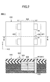
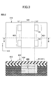
- FIG. It is a figure which shows roughly the control board 400-1 of the inverter 4 by an example. It is a figure which shows schematically the control board 400-2 of the inverter 4 by another example.
- FIG. 1 is a diagram illustrating an example of an electric circuit 1 including an inverter 4.
- the electric circuit 1 is for driving a motor, for example.
- the electric circuit 1 includes a battery 2, an inverter (an example of a power converter) 4, a smoothing capacitor C1, and a discharge resistor R1.
- a motor (not shown) is connected to the inverter 4.
- the motor may be a traveling motor used in a hybrid vehicle or an electric vehicle.
- the smoothing capacitor C1 is connected between the positive electrode side and the negative electrode side of the battery 2.
- the discharge resistor R1 is connected in parallel with the smoothing capacitor C1 between the positive electrode side and the negative electrode side of the battery 2.
- a plurality of discharge resistors R1 are connected in series, and the plurality of discharge resistors R1 connected in series are connected in parallel to the smoothing capacitor C1.
- the discharge resistor R1 has a function of releasing (discharging) the electric charge of the smoothing capacitor C1 to the ground. Such discharge may be realized constantly during the operation of the inverter 4 or may be realized when a relay (not shown) is turned off (when the operation of the inverter 4 ends). During this discharge, the discharge resistor R1 generates heat.
- a DC-DC converter (another example of the power conversion device) may be provided between the smoothing capacitor C1 and the battery 2.
- FIG. 2 is a diagram schematically showing a control board 400-1 of the inverter 4 according to an example.
- the upper side of FIG. 2 is a top view, and the lower side of FIG. 2 is along the line BB in the upper side of FIG. It is sectional drawing.
- the top view refers to a mode in which the surface is viewed in a direction perpendicular to the surface of the substrate body 410 (a direction perpendicular to the surface).
- the X direction and the Y direction are defined with reference to the rectangular outer shape of the substrate body 410, and the upper side on the lower side of FIG.
- the direction of the control board 400-1 of the inverter 4 differs depending on the mounting state of the control board 400-1 of the inverter 4, and the upward direction does not necessarily correspond to the vertical upward direction.
- the control board 400-1 includes a board body 410, a first circuit part 421, a second circuit part 422, an insulating region 424, and a pattern 426.
- the substrate body 410 is a multilayer substrate.
- the substrate body 410 preferably has two or more inner layers. In the example illustrated in FIG. 2, the substrate body 410 has four inner layers.
- the first circuit unit 421 includes a discharge resistor R1 (an example of a heat generating component) mounted on the upper surface (an example of the first surface) of the substrate body 410.
- the plurality of discharge resistors R1 are arranged in a line in the Y direction.
- the plurality of discharge resistors R1 may be arranged in a plurality of rows in the Y direction.
- the second circuit unit 422 is mounted on the upper surface of the substrate body 410.
- the second circuit unit 422 is different in voltage from the first circuit unit 421.
- “Different voltages” means that the voltages handled are different, and typically the power supply voltages are different.
- the voltage difference between the second circuit unit 422 and the first circuit unit 421 is, for example, several tens V or more, and typically 100 V or more.
- the second circuit unit 422 includes a circuit unit that forms a microcomputer that controls the inverter 4.
- the first circuit unit 421 forms a high voltage system circuit corresponding to the voltage of the electric circuit 1, while the second circuit unit 422 forms a low voltage system circuit.
- a rectangle that schematically represents the second circuit unit 422 represents resistance.
- the insulating region 424 is formed on the upper surface of the substrate body 410.
- the insulating region 424 insulates the first circuit portion 421 and the second circuit portion 422 from each other.
- the insulating region 424 is a region that does not have a conductor portion, and may be a region where no electronic component is mounted.
- the insulating region 424 may be formed of a material having a higher CTI (Comparative Tracking Index) than the material of the substrate body 410.
- the insulating region 424 is formed between the first circuit portion 421 and the second circuit portion 422 so as to ensure a minimum creepage distance defined by, for example, JIS.
- the insulating region 424 is preferably formed adjacent to the first circuit portion 421. In the example shown in FIG.
- the insulating region 424 is formed between lines L1 and L2 extending in the Y direction in the X direction.
- the line L1 is a line segment circumscribing from the first circuit portion 421 side to a component group forming the second circuit portion 422 in a top view.
- the line L2 is a line segment circumscribing the component group forming the first circuit portion 421 from the second circuit portion 422 side in a top view.
- the insulating region 424 is adjacent to both the first circuit portion 421 and the second circuit portion 422.
- the shape of the insulating region 424 in the top view is arbitrary, and may be a shape other than a rectangle.
- the lines L1 and L2 may have a bent portion or a curved portion.
- the insulating region 424 is formed over the entire Y direction on the upper surface of the substrate body 410, but may be formed only in a part in the Y direction.
- the pattern 426 is formed in the inner layer of the substrate body 410.
- the pattern 426 may be formed in any layer as long as it is an inner layer of the substrate body 410, and the number of layers formed is also arbitrary. In the example shown in FIG. 2, the pattern 426 is formed on all inner layers of the substrate body 410.
- the pattern 426 is formed of a heat conductive material, for example, a copper solid pattern.
- the pattern 426 extends in a region overlapping the insulating region 424 when viewed from above.
- the pattern 426 may extend in a region overlapping the entire insulating region 424 in the top view with respect to the X direction, or may extend in a region overlapping a part of the insulating region 424 in the top view.
- the pattern 426 may extend in a region overlapping with the entire insulating region 424 in a top view in the Y direction, or may extend in a region overlapping with a part of the insulating region 424 in a top view.
- the pattern 426 extends in a region overlapping the entire insulating region 424 in the X direction when viewed from above.
- the cross section of the pattern 426 shown in the lower side of FIG. 2 may be an equal cross section in the Y direction.
- the pattern 426 extends in a region overlapping the entire insulating region 424 in the Y direction when viewed from above.
- the pattern 426 is exposed to the outside of the substrate body 410 on the side surface of the substrate body 410 in the Y direction.
- the pattern 426 is thermally connected to the discharge resistor R1.
- the pattern 426 is connected to the discharge resistor R ⁇ b> 1 through the through via 430.
- the through via 430 may be formed for a part of the plurality of discharge resistors R1, may be formed for each discharge resistor R1, or may be formed between the discharge resistors R1 in the Y direction. Also good.
- the through via 430 may be electrically insulated from the discharge resistor R1, or may be electrically connected to the discharge resistor R1. When a plurality of through vias 430 are electrically connected to the corresponding discharge resistors R1, each discharge resistor R1 is connected in series via the plurality of through vias 430 and the pattern 426.
- the discharge resistor R1 is a heat generating component and requires a heat dissipation structure.
- the pattern 426 is formed of a heat conductive material and is thermally connected to the discharge resistor R1, and thus can function as a heat radiating portion.
- the pattern 426 extends in a region overlapping the insulating region 424 in a top view as described above, the heat dissipation function can be realized in a manner with less restrictions on the component mounting range. For example, in the example shown in FIG.
- the component mounting range on the lower surface of the board body 410 is restricted.
- the control board 400-1 of the inverter 4 shown in FIG. 2 since the heat radiating portion is formed using the inner layer, the components on the surface of the board body 410 (the lower surface in this example).
- the heat dissipation function can be realized in a mode with few restrictions on the mounting range.
- substrate body 410 is an area
- the pattern 426 is formed in the entire inner layer, the area overlapping the insulating region 424 in the inner layer of the substrate body 410 is fully utilized (maximizing the mass) to improve the heat dissipation performance. Can be increased.
- the insulating region 424 is formed adjacent to the first circuit portion 421, the pattern 426 does not overlap with circuit portions other than the first circuit portion 421 in a top view. It can extend from the first circuit portion 421 side to a region overlapping the insulating region 424 when viewed from above. Thereby, a heat dissipation function can be realized without impairing the possibility that the inner layer of the substrate body 410 can be used for wiring with respect to circuit parts other than the first circuit part 421.
- FIG. 3 is a diagram schematically showing a control board 400-2 of the inverter 4 according to another example.
- the upper side of FIG. 3 shows a top view, and the lower side of FIG. 3 shows the line BB on the upper side of FIG. FIG.
- the control board 400-2 is different from the control board 400-1 shown in FIG. 2 only in that the through via 430 does not exist.
- Other configurations that may be the same are denoted by the same reference numerals and description thereof is omitted.
- the thermal connection mode between the pattern 426 and the discharge resistor R1 is arbitrary, and the through via 430 may not be used.
- the heat generating component is the discharge resistor R1 that has a high need for heat dissipation, but the heat generating component is an arbitrary component mounted on the control board 400-1 (control board 400-2). There may be.
- the heat generating component may be a microcomputer chip.
- the insulating region 424 is formed adjacent to the first circuit portion 421, but the insulating region 424 may not be adjacent to the first circuit portion 421. That is, another circuit unit may be formed between the insulating region 424 and the first circuit unit 421.
- control board 400-1 (control board 400-2) of the inverter 4 is used, but is not limited thereto.
- a DC-DC converter another example of a power converter
- the control board 400-1 (control board 400-2)
- a control board for the DC-DC converter may be formed.
- the pattern 426 is a solid pattern formed over a wide range in both the X direction and the Y direction.
- the pattern 426 includes a plurality of linear patterns extending in the X direction or the Y direction. It may be formed by a set.
- a substrate body 410 which is a multilayer substrate;
- a first circuit unit 421 including a heat generating component (R1) mounted on the first surface of the substrate body 410;
- a second circuit part 422 mounted on the first surface of the substrate body 410 and having a voltage different from that of the first circuit part 421;
- An insulating region 424 that is formed on a first surface of the substrate body 410 and insulates between the first circuit portion 421 and the second circuit portion 422; Formed in an inner layer of the substrate body 410, extends in a region overlapping the insulating region 424 when viewed in a direction perpendicular to the first surface of the substrate body 410, and is thermally connected to the heat generating component (R1).
- a control board 400-1, 400-2 of the power converter including a pattern 426 of heat conductive material.
- the pattern 426 is a thermally conductive material and is thermally connected to the heat generating component (R1), it can function as a heat radiating portion. Further, since the pattern 426 extends in a region overlapping the insulating region 424 when viewed in the direction perpendicular to the first surface of the substrate body 410, a region (so-called dead space) that is not used for wiring in the inner layer of the substrate body 410 is formed. Can be formed using. As a result, the heat radiation function can be realized in a manner with less restrictions on the component mounting range on the surface of the board body 410.
- the insulating region 424 is formed on the control boards 400-1 and 400-2 of the power conversion device according to (1), which is formed adjacent to the first circuit portion 421.
- the pattern 426 is viewed in a direction perpendicular to the first surface of the substrate body 410,
- the circuit portion other than the first circuit portion 421 can be extended to a region overlapping the insulating region 424 without overlapping.
- a heat dissipation function can be realized without impairing the possibility that the inner layer of the substrate body 410 can be used for wiring with respect to circuit parts other than the first circuit part 421.
- the heat generating component (R1) is a discharge resistor, the control boards 400-1 and 400-2 of the power conversion device according to (1) or (2).
- the discharge resistance having a large calorific value can be efficiently radiated by the pattern 426.
- the power converter is an inverter 4 provided in parallel with the smoothing capacitor C1
- the discharge resistor R1 of the first circuit unit 421 has a function of discharging the charge of the smoothing capacitor C1
- Said 2nd circuit part 422 is a control board of the power converter device as described in (3) containing the control circuit part for controlling the said inverter 4.
Landscapes
- Engineering & Computer Science (AREA)
- Microelectronics & Electronic Packaging (AREA)
- Power Engineering (AREA)
- Inverter Devices (AREA)
- Structure Of Printed Boards (AREA)
Abstract
電力変換装置の制御基板は、多層基板である基板本体と、前記基板本体の第1表面に実装される発熱部品を含む第1回路部と、前記基板本体の第1表面に実装され、前記第1回路部に対して電圧が異なる第2回路部と、前記基板本体の第1表面に形成され、前記第1回路部と前記第2回路部間を絶縁する絶縁領域と、前記基板本体の内層に形成され、前記基板本体の第1表面に対して垂直方向に視て前記絶縁領域に重なる領域に延在し、前記発熱部品に熱的に接続される熱伝導性材料のパターンとを含む。
Description
本開示は、電力変換装置の制御基板に関する。
直列接続された3つ以上の抵抗からなり、平滑コンデンサに蓄積された電荷の放電する抵抗回路を備え、両端以外に配置される抵抗の抵抗値が、両端に配置される抵抗の抵抗値より小さくなるように設定された電子装置が知られている(例えば、特許文献1参照)。
しかしながら、特許文献1に記載の電子装置では、抵抗回路の放熱用パターンは、基板の表面に形成されているので、放熱用パターンに起因して基板の表面における部品実装範囲が制約を受けるという問題がある。
そこで、本開示は、部品実装範囲への制約が少ない態様で放熱機能を実現できる電力変換装置の制御基板の提供を目的とする。
本開示の一局面によれば、多層基板である基板本体と、
前記基板本体の第1表面に実装される発熱部品を含む第1回路部と、
前記基板本体の第1表面に実装され、前記第1回路部に対して電圧が異なる第2回路部と、
前記基板本体の第1表面に形成され、前記第1回路部と前記第2回路部間を絶縁する絶縁領域と、
前記基板本体の内層に形成され、前記基板本体の第1表面に対して垂直方向に視て前記絶縁領域に重なる領域に延在し、前記発熱部品に熱的に接続される熱伝導性材料のパターンとを含む、電力変換装置の制御基板が提供される。
前記基板本体の第1表面に実装される発熱部品を含む第1回路部と、
前記基板本体の第1表面に実装され、前記第1回路部に対して電圧が異なる第2回路部と、
前記基板本体の第1表面に形成され、前記第1回路部と前記第2回路部間を絶縁する絶縁領域と、
前記基板本体の内層に形成され、前記基板本体の第1表面に対して垂直方向に視て前記絶縁領域に重なる領域に延在し、前記発熱部品に熱的に接続される熱伝導性材料のパターンとを含む、電力変換装置の制御基板が提供される。
本開示によれば、部品実装範囲への制約が少ない態様で放熱機能を実現できる電力変換装置の制御基板が得られる。
以下、添付図面を参照しながら各実施例について詳細に説明する。
図1は、インバータ4を含む電気回路1の一例を示す図である。電気回路1は、例えばモータ駆動用である。
電気回路1は、バッテリ2と、インバータ(電力変換装置の一例)4と、平滑コンデンサC1と、放電抵抗R1とを含む。インバータ4には、モータ(図示せず)が接続される。モータは、ハイブリッド車又は電気自動車で使用される走行用モータであってよい。
平滑コンデンサC1は、バッテリ2の正極側と負極側との間に接続される。
放電抵抗R1は、バッテリ2の正極側と負極側との間に、平滑コンデンサC1に対し並列に接続される。図1に示す例では、複数の放電抵抗R1が直列に接続され、直列接続された複数の放電抵抗R1が、平滑コンデンサC1に対し並列に接続されている。放電抵抗R1は、平滑コンデンサC1の電荷をグランドに逃がす(放電させる)機能を有する。かかる放電は、インバータ4の動作中に常時実現されてもよいし、リレー(図示せず)がオフしたとき(インバータ4の動作終了時)に実現されてもよい。この放電の際、放電抵抗R1は発熱する。
尚、図1に示す例において、平滑コンデンサC1とバッテリ2との間には、DC-DCコンバータ(電力変換装置の他の一例)が設けられてもよい。
図2は、一例によるインバータ4の制御基板400-1を概略的に示す図であり、図2上側は、上面視を示し、図2下側は、図2上側におけるラインB-Bに沿った断面図である。尚、上面視とは、基板本体410の表面に対して垂直方向(面直方向)に視る態様をいう。以下では、便宜上、図2上側に示すように基板本体410の矩形の外形を基準としてX方向及びY方向を定義し、図2下側における上側を上方向とする。但し、インバータ4の制御基板400-1の向きは、インバータ4の制御基板400-1の実装状態に応じて異なり、必ずしも上方向が鉛直上方向に対応するとは限らない。
制御基板400-1は、基板本体410と、第1回路部421と、第2回路部422と、絶縁領域424と、パターン426とを含む。
基板本体410は、多層基板である。基板本体410は、好ましくは、2層以上の内層を有する。図2に示す例では、基板本体410は、4層の内層を有する。
第1回路部421は、基板本体410の上側の表面(第1表面の一例)に実装される放電抵抗R1(発熱部品の一例)を含む。図2に示す例では、複数個の放電抵抗R1は、Y方向に一列に並べられている。但し、複数個の放電抵抗R1は、Y方向に複数列で並べられてもよい。
第2回路部422は、基板本体410の上側の表面に実装される。第2回路部422は、第1回路部421に対して電圧が異なる。「電圧が異なる」とは、扱う電圧が異なること意味し、典型的には、電源電圧が異なることを意味する。第2回路部422と第1回路部421との間の電圧の違いは、例えば、数十V以上であり、典型的には、100V以上である。例えば、第2回路部422は、インバータ4を制御するマイクロコンピューター(マイコン)を形成する回路部を含む。この場合、第1回路部421は、電気回路1の電圧に対応する高電圧系回路を形成するが、第2回路部422は、低電圧系回路を形成する。尚、図2に示す例では、第2回路部422を概略的に表す矩形は、抵抗を表す。
絶縁領域424は、基板本体410の上側の表面に形成される。絶縁領域424は、第1回路部421と第2回路部422間を絶縁する。絶縁領域424は、導体部を有しない領域であり、何ら電子部品が実装されない領域であってよい。絶縁領域424は、基板本体410の材料よりも高いCTI(Comparative Tracking Index)を持つ材料により形成されてもよい。絶縁領域424は、第1回路部421と第2回路部422間に、例えばJIS等で規定される最小沿面距離が確保されるように形成される。絶縁領域424は、好ましくは、第1回路部421に隣接して形成される。図2に示す例では、絶縁領域424は、X方向におけるY方向に延びるラインL1とL2との間に形成される。ラインL1は、上面視で、第2回路部422を形成する部品群に第1回路部421側から外接する線分である。同様に、ラインL2は、上面視で、第1回路部421を形成する部品群に第2回路部422側から外接する線分である。従って、絶縁領域424は、第1回路部421及び第2回路部422の双方に隣接する。尚、上面視における絶縁領域424の形状は、任意であり、矩形以外の形状であってもよい。即ち、ラインL1,L2は、屈曲部や湾曲部を有してもよい。また、図2に示す例では、絶縁領域424は、基板本体410の上側の表面においてY方向全体に亘って形成されているが、Y方向の一部のみに形成されてもよい。
パターン426は、基板本体410の内層に形成される。パターン426は、基板本体410の内層であれば、任意の層に形成されてもよく、形成される層数も任意である。図2に示す例では、パターン426は、基板本体410の内層全てに形成される。パターン426は、熱伝導性材料により形成され、例えば銅のベタパターンにより形成される。
パターン426は、上面視で絶縁領域424に重なる領域に延在する。パターン426は、X方向に関して、上面視で絶縁領域424全体に重なる領域に延在してもよいし、上面視で絶縁領域424の一部と重なる領域に延在してもよい。同様に、パターン426は、Y方向に関して、上面視で絶縁領域424全体に重なる領域に延在してもよいし、上面視で絶縁領域424の一部と重なる領域に延在してもよい。図2に示す例では、パターン426は、上面視で、X方向で絶縁領域424全体に重なる領域に延在する。また、図2下側に示すパターン426の断面はY方向に等断面であって良く、この場合、パターン426は、上面視で、Y方向で絶縁領域424全体に重なる領域に延在する。尚、この場合、パターン426は、基板本体410のY方向の側面にて基板本体410の外部に露出することになる。
パターン426は、放電抵抗R1に熱的に接続される。図2に示す例では、パターン426は、貫通ビア430を介して放電抵抗R1に接続される。貫通ビア430は、複数の放電抵抗R1のうちの一部に対して形成されてもよいし、各放電抵抗R1に対して形成されてもよいし、Y方向における放電抵抗R1間に形成されてもよい。貫通ビア430は、放電抵抗R1に電気的に絶縁されていてもよいし、放電抵抗R1に電気的に接続されてもよい。尚、複数の貫通ビア430が対応する各放電抵抗R1に電気的に接続される場合は、各放電抵抗R1は、複数の貫通ビア430及びパターン426を介して直列接続されることになる。
ところで、上述の如く放電抵抗R1は発熱部品であり、放熱構造が必要である。この点、図2に示すインバータ4の制御基板400-1によれば、パターン426は、熱伝導性材料により形成され且つ放電抵抗R1に熱的に接続されるので、放熱部として機能できる。また、パターン426は、上述の如く上面視で絶縁領域424に重なる領域に延在するので、部品実装範囲への制約が少ない態様で放熱機能を実現できる。例えば図2に示す例において、仮にパターン426が基板本体410の下側の表面に形成されている場合は、基板本体410の下側の表面における部品実装範囲が制約を受ける。これに対して、図2に示すインバータ4の制御基板400-1によれば、内層を利用して放熱部を形成するので、基板本体410の表面(本例では、下側の表面)における部品実装範囲への制約が少ない態様で放熱機能を実現できる。また、基板本体410の内層における絶縁領域424と重なる領域は、配線に利用されない領域(いわゆるデッドスペース)であるので、かかる領域を利用して効率的に放熱機能を実現できる。
また、特に図2に示す例では、パターン426が全内層に形成されるので、基板本体410の内層における絶縁領域424と重なる領域をフルに利用して(マスを最大化して)、放熱性能を高めることができる。また、図2に示す例では、絶縁領域424は、第1回路部421に隣接して形成されるので、パターン426は、第1回路部421以外の回路部とは上面視で重ならずに、上面視で第1回路部421側から絶縁領域424に重なる領域まで延在できる。これにより、第1回路部421以外の回路部に対して基板本体410の内層を配線用に利用できる可能性を損なうことなく、放熱機能を実現できる。
図3は、他の一例によるインバータ4の制御基板400-2を概略的に示す図であり、図3上側は、上面視を示し、図3下側は、図3上側におけるラインB-Bに沿った断面図である。
制御基板400-2は、貫通ビア430が存在しない点のみが、図2に示した制御基板400-1と異なる。他の同一であってよい構成については、同一の参照符号を付して説明を省略する。
図3に示すインバータ4の制御基板400-2によっても、インバータ4の制御基板400-1と同様の効果が奏される。このようにパターン426と放電抵抗R1との間の熱的な接続態様は、任意であり、貫通ビア430を利用しなくてもよい。
以上、各実施例について詳述したが、特定の実施例に限定されるものではなく、特許請求の範囲に記載された範囲内において、種々の変形及び変更が可能である。また、前述した実施例の構成要素を全部又は複数を組み合わせることも可能である。
例えば、上述した実施例では、発熱部品は、放熱の必要性が高い放電抵抗R1であるが、発熱部品は、制御基板400-1(制御基板400-2)上に実装される任意の部品であってもよい。例えば、発熱部品は、マイコンのチップであってもよい。
また、上述した実施例では、絶縁領域424は、第1回路部421に隣接して形成されているが、絶縁領域424は、第1回路部421に隣接していなくてもよい。即ち、絶縁領域424と第1回路部421との間には、他の回路部が形成されてもよい。
また、上述した実施例では、インバータ4の制御基板400-1(制御基板400-2)であるが、これに限られない。例えば、平滑コンデンサC1とバッテリ2との間には、DC-DCコンバータ(電力変換装置の他の一例)が設けられる場合は、制御基板400-1(制御基板400-2)は、インバータ4の制御基板に代えて又は加えて、DC-DCコンバータの制御基板を形成してもよい。
また、上述した実施例では、パターン426は、X方向及びY方向の双方において広範囲に亘って形成されるベタパターンであったが、X方向又はY方向に延在する複数の線状のパターンの集合により形成されてもよい。
なお、以上の実施例に関し、さらに以下を開示する。
(1)
多層基板である基板本体410と、
前記基板本体410の第1表面に実装される発熱部品(R1)を含む第1回路部421と、
前記基板本体410の第1表面に実装され、前記第1回路部421に対して電圧が異なる第2回路部422と、
前記基板本体410の第1表面に形成され、前記第1回路部421と前記第2回路部422間を絶縁する絶縁領域424と、
前記基板本体410の内層に形成され、前記基板本体410の第1表面に対して垂直方向に視て前記絶縁領域424に重なる領域に延在し、前記発熱部品(R1)に熱的に接続される熱伝導性材料のパターン426とを含む、電力変換装置の制御基板400-1、400-2。
(1)
多層基板である基板本体410と、
前記基板本体410の第1表面に実装される発熱部品(R1)を含む第1回路部421と、
前記基板本体410の第1表面に実装され、前記第1回路部421に対して電圧が異なる第2回路部422と、
前記基板本体410の第1表面に形成され、前記第1回路部421と前記第2回路部422間を絶縁する絶縁領域424と、
前記基板本体410の内層に形成され、前記基板本体410の第1表面に対して垂直方向に視て前記絶縁領域424に重なる領域に延在し、前記発熱部品(R1)に熱的に接続される熱伝導性材料のパターン426とを含む、電力変換装置の制御基板400-1、400-2。
(1)に記載の構成によれば、パターン426は、熱伝導性材料であり且つ発熱部品(R1)に熱的に接続されるので、放熱部として機能することができる。また、パターン426は、基板本体410の第1表面に対して垂直方向に視て絶縁領域424に重なる領域に延在するので、基板本体410の内層における配線に利用されない領域(いわゆるデッドスペース)を利用して形成できる。これにより、基板本体410の表面における部品実装範囲への制約が少ない態様で放熱機能を実現できる。
(2)
前記絶縁領域424は、前記第1回路部421に隣接して形成される、(1)に記載の電力変換装置の制御基板400-1、400-2。
(2)
前記絶縁領域424は、前記第1回路部421に隣接して形成される、(1)に記載の電力変換装置の制御基板400-1、400-2。
(2)に記載の構成によれば、絶縁領域424は、第1回路部421に隣接して形成されるので、パターン426は、基板本体410の第1表面に対して垂直方向に視て、第1回路部421以外の回路部とは重ならずに、絶縁領域424に重なる領域まで延在できる。これにより、第1回路部421以外の回路部に対して基板本体410の内層を配線用に利用できる可能性を損なうことなく、放熱機能を実現できる。
(3)
前記発熱部品(R1)は、放電抵抗である、(1)又は(2)に記載の電力変換装置の制御基板400-1、400-2。
(3)
前記発熱部品(R1)は、放電抵抗である、(1)又は(2)に記載の電力変換装置の制御基板400-1、400-2。
(3)に記載の構成によれば、発熱量が大きい放電抵抗をパターン426により効率的に放熱させることができる。
(4)
前記電力変換装置は、平滑コンデンサC1に並列に設けられるインバータ4であり、
前記第1回路部421の前記放電抵抗R1は、前記平滑コンデンサC1の電荷を放電する機能を備え、
前記第2回路部422は、前記インバータ4を制御するための制御回路部を含む、(3)に記載の電力変換装置の制御基板。
(4)
前記電力変換装置は、平滑コンデンサC1に並列に設けられるインバータ4であり、
前記第1回路部421の前記放電抵抗R1は、前記平滑コンデンサC1の電荷を放電する機能を備え、
前記第2回路部422は、前記インバータ4を制御するための制御回路部を含む、(3)に記載の電力変換装置の制御基板。
なお、本国際出願は、2014年7月31日に出願した日本国特許出願2014-156768号に基づく優先権を主張するものであり、その全内容は本国際出願にここでの参照により援用されるものとする。
1 電気回路
4 インバータ
400-1,400-2 制御基板
410 基板本体
421 第1回路部
422 第2回路部
424 絶縁領域
426 パターン
4 インバータ
400-1,400-2 制御基板
410 基板本体
421 第1回路部
422 第2回路部
424 絶縁領域
426 パターン
Claims (4)
- 多層基板である基板本体と、
前記基板本体の第1表面に実装される発熱部品を含む第1回路部と、
前記基板本体の第1表面に実装され、前記第1回路部に対して電圧が異なる第2回路部と、
前記基板本体の第1表面に形成され、前記第1回路部と前記第2回路部間を絶縁する絶縁領域と、
前記基板本体の内層に形成され、前記基板本体の第1表面に対して垂直方向に視て前記絶縁領域に重なる領域に延在し、前記発熱部品に熱的に接続される熱伝導性材料のパターンとを含む、電力変換装置の制御基板。 - 前記絶縁領域は、前記第1回路部に隣接して形成される、請求項1に記載の電力変換装置の制御基板。
- 前記発熱部品は、放電抵抗である、請求項1又は2に記載の電力変換装置の制御基板。
- 前記電力変換装置は、平滑コンデンサに並列に設けられるインバータであり、
前記第1回路部の前記放電抵抗は、前記平滑コンデンサの電荷を放電する機能を備え、
前記第2回路部は、前記インバータを制御するための制御回路部を含む、請求項3に記載の電力変換装置の制御基板。
Priority Applications (3)
| Application Number | Priority Date | Filing Date | Title |
|---|---|---|---|
| CN201580035231.9A CN106664791A (zh) | 2014-07-31 | 2015-07-08 | 电力转换装置的控制基板 |
| US15/322,961 US20170141697A1 (en) | 2014-07-31 | 2015-07-08 | Control board for power conversion device |
| DE112015002674.6T DE112015002674T5 (de) | 2014-07-31 | 2015-07-08 | Steuerungsplatine für eine Leistungswandlervorrichtung |
Applications Claiming Priority (2)
| Application Number | Priority Date | Filing Date | Title |
|---|---|---|---|
| JP2014-156768 | 2014-07-31 | ||
| JP2014156768A JP2016033973A (ja) | 2014-07-31 | 2014-07-31 | 電力変換装置の制御基板 |
Publications (1)
| Publication Number | Publication Date |
|---|---|
| WO2016017390A1 true WO2016017390A1 (ja) | 2016-02-04 |
Family
ID=55217295
Family Applications (1)
| Application Number | Title | Priority Date | Filing Date |
|---|---|---|---|
| PCT/JP2015/069682 Ceased WO2016017390A1 (ja) | 2014-07-31 | 2015-07-08 | 電力変換装置の制御基板 |
Country Status (5)
| Country | Link |
|---|---|
| US (1) | US20170141697A1 (ja) |
| JP (1) | JP2016033973A (ja) |
| CN (1) | CN106664791A (ja) |
| DE (1) | DE112015002674T5 (ja) |
| WO (1) | WO2016017390A1 (ja) |
Families Citing this family (1)
| Publication number | Priority date | Publication date | Assignee | Title |
|---|---|---|---|---|
| JP7318732B2 (ja) * | 2019-11-25 | 2023-08-01 | 株式会社アイシン | 制御基板 |
Citations (2)
| Publication number | Priority date | Publication date | Assignee | Title |
|---|---|---|---|---|
| JP2005191378A (ja) * | 2003-12-26 | 2005-07-14 | Toyota Industries Corp | プリント基板における放熱構造 |
| JP2012039715A (ja) * | 2010-08-05 | 2012-02-23 | Denso Corp | 電子装置 |
Family Cites Families (12)
| Publication number | Priority date | Publication date | Assignee | Title |
|---|---|---|---|---|
| JPS6013485A (ja) * | 1983-07-01 | 1985-01-23 | Matsushita Electric Ind Co Ltd | 誘導電動機駆動用インバ−タ装置 |
| US6068400A (en) * | 1998-02-27 | 2000-05-30 | Tektronix, Inc. | Temperature compensated adapter for a DMM |
| US6293700B1 (en) * | 1999-09-24 | 2001-09-25 | Fluke Corporation | Calibrated isothermal assembly for a thermocouple thermometer |
| US6423940B1 (en) * | 2001-03-02 | 2002-07-23 | Agilent Technologies, Inc. | Temperature stabilization scheme for a circuit board |
| JP3589997B2 (ja) * | 2001-03-30 | 2004-11-17 | 株式会社東芝 | 赤外線センサおよびその製造方法 |
| DE102004041027B4 (de) * | 2004-08-25 | 2007-01-18 | Infineon Technologies Ag | Speichermodul |
| FR2913173B1 (fr) * | 2007-02-22 | 2009-05-15 | Airbus France Sa | Carte electronique et aeronef la comportant |
| JP5193660B2 (ja) * | 2008-04-03 | 2013-05-08 | 株式会社日立製作所 | 電池モジュール及びそれを備えた蓄電装置並びに電機システム |
| JP2010220286A (ja) * | 2009-03-13 | 2010-09-30 | Aisin Seiki Co Ltd | モータ制御装置および車両システム |
| CN102460693A (zh) * | 2009-06-19 | 2012-05-16 | 株式会社安川电机 | 电力变换装置 |
| US8411442B2 (en) * | 2010-09-09 | 2013-04-02 | Texas Instruments Incorporated | Vias in substrate between IC seat and peripheral thermal cage |
| JP5534353B2 (ja) * | 2011-03-31 | 2014-06-25 | アイシン・エィ・ダブリュ株式会社 | インバータ装置 |
-
2014
- 2014-07-31 JP JP2014156768A patent/JP2016033973A/ja active Pending
-
2015
- 2015-07-08 CN CN201580035231.9A patent/CN106664791A/zh active Pending
- 2015-07-08 WO PCT/JP2015/069682 patent/WO2016017390A1/ja not_active Ceased
- 2015-07-08 US US15/322,961 patent/US20170141697A1/en not_active Abandoned
- 2015-07-08 DE DE112015002674.6T patent/DE112015002674T5/de not_active Withdrawn
Patent Citations (2)
| Publication number | Priority date | Publication date | Assignee | Title |
|---|---|---|---|---|
| JP2005191378A (ja) * | 2003-12-26 | 2005-07-14 | Toyota Industries Corp | プリント基板における放熱構造 |
| JP2012039715A (ja) * | 2010-08-05 | 2012-02-23 | Denso Corp | 電子装置 |
Also Published As
| Publication number | Publication date |
|---|---|
| CN106664791A (zh) | 2017-05-10 |
| US20170141697A1 (en) | 2017-05-18 |
| JP2016033973A (ja) | 2016-03-10 |
| DE112015002674T5 (de) | 2017-03-02 |
Similar Documents
| Publication | Publication Date | Title |
|---|---|---|
| US11153966B2 (en) | Electronic circuit device | |
| JP6859304B2 (ja) | メインバッテリ用バッテリモジュール | |
| JP6237554B2 (ja) | 電力変換装置の制御基板 | |
| JP5469270B1 (ja) | 電子機器 | |
| JP2012059759A (ja) | 電子制御ユニット | |
| JP6471659B2 (ja) | インバータ制御基板 | |
| WO2018116667A1 (ja) | 電力変換装置 | |
| JP6365362B2 (ja) | 電力変換装置用の制御基板 | |
| JP2009027778A (ja) | バスバー | |
| JP6176135B2 (ja) | 電力変換装置 | |
| JP7390835B2 (ja) | 電子装置 | |
| JP2022188354A (ja) | 電力変換装置 | |
| JP6699535B2 (ja) | 回路基板 | |
| JP2013003714A (ja) | 電源装置および車両用電子制御装置 | |
| JP7052609B2 (ja) | 電力変換装置 | |
| JP2016033973A (ja) | 電力変換装置の制御基板 | |
| JP6973313B2 (ja) | 電力変換装置 | |
| JP5846929B2 (ja) | パワー半導体モジュール | |
| JP6203232B2 (ja) | パワーモジュール | |
| JP6794757B2 (ja) | 電子回路装置 | |
| JP6683020B2 (ja) | 電力変換装置、及び、これを用いた電動パワーステアリング装置 | |
| JP5992028B2 (ja) | 回路基板 | |
| JP7357710B2 (ja) | 電力変換装置 | |
| JP6390166B2 (ja) | 電源装置 | |
| JP7745525B2 (ja) | 放電抵抗回路及びそれを用いた電力変換装置 |
Legal Events
| Date | Code | Title | Description |
|---|---|---|---|
| 121 | Ep: the epo has been informed by wipo that ep was designated in this application |
Ref document number: 15828111 Country of ref document: EP Kind code of ref document: A1 |
|
| WWE | Wipo information: entry into national phase |
Ref document number: 15322961 Country of ref document: US |
|
| WWE | Wipo information: entry into national phase |
Ref document number: 112015002674 Country of ref document: DE |
|
| 122 | Ep: pct application non-entry in european phase |
Ref document number: 15828111 Country of ref document: EP Kind code of ref document: A1 |