WO2016017299A1 - 回路基板の実装構造、それを用いたセンサ - Google Patents
回路基板の実装構造、それを用いたセンサ Download PDFInfo
- Publication number
- WO2016017299A1 WO2016017299A1 PCT/JP2015/067110 JP2015067110W WO2016017299A1 WO 2016017299 A1 WO2016017299 A1 WO 2016017299A1 JP 2015067110 W JP2015067110 W JP 2015067110W WO 2016017299 A1 WO2016017299 A1 WO 2016017299A1
- Authority
- WO
- WIPO (PCT)
- Prior art keywords
- circuit board
- resin
- printed circuit
- circuit module
- sensor
- Prior art date
Links
- 229920005989 resin Polymers 0.000 claims abstract description 36
- 239000011347 resin Substances 0.000 claims abstract description 36
- 239000004065 semiconductor Substances 0.000 claims abstract description 35
- 239000000463 material Substances 0.000 claims abstract description 8
- 239000004020 conductor Substances 0.000 claims description 14
- 238000000465 moulding Methods 0.000 abstract description 18
- 238000000034 method Methods 0.000 description 11
- 239000000853 adhesive Substances 0.000 description 8
- 230000001070 adhesive effect Effects 0.000 description 6
- 239000002184 metal Substances 0.000 description 6
- 239000000758 substrate Substances 0.000 description 6
- 238000002485 combustion reaction Methods 0.000 description 3
- 239000011521 glass Substances 0.000 description 3
- 238000005304 joining Methods 0.000 description 3
- 238000004519 manufacturing process Methods 0.000 description 3
- 238000004382 potting Methods 0.000 description 3
- 230000035882 stress Effects 0.000 description 3
- 230000006866 deterioration Effects 0.000 description 2
- 239000003822 epoxy resin Substances 0.000 description 2
- 239000010445 mica Substances 0.000 description 2
- 229910052618 mica group Inorganic materials 0.000 description 2
- 229920000647 polyepoxide Polymers 0.000 description 2
- 238000000926 separation method Methods 0.000 description 2
- 230000008646 thermal stress Effects 0.000 description 2
- 229920005992 thermoplastic resin Polymers 0.000 description 2
- 229920001187 thermosetting polymer Polymers 0.000 description 2
- 239000004925 Acrylic resin Substances 0.000 description 1
- 229920000178 Acrylic resin Polymers 0.000 description 1
- 230000005483 Hooke's law Effects 0.000 description 1
- 239000004642 Polyimide Substances 0.000 description 1
- 238000005336 cracking Methods 0.000 description 1
- 238000005520 cutting process Methods 0.000 description 1
- 238000001514 detection method Methods 0.000 description 1
- 239000000945 filler Substances 0.000 description 1
- 239000000446 fuel Substances 0.000 description 1
- 239000003365 glass fiber Substances 0.000 description 1
- 238000002347 injection Methods 0.000 description 1
- 239000007924 injection Substances 0.000 description 1
- 238000009434 installation Methods 0.000 description 1
- 238000011900 installation process Methods 0.000 description 1
- 238000005259 measurement Methods 0.000 description 1
- 238000012986 modification Methods 0.000 description 1
- 230000004048 modification Effects 0.000 description 1
- 239000005011 phenolic resin Substances 0.000 description 1
- 229920000515 polycarbonate Polymers 0.000 description 1
- 239000004417 polycarbonate Substances 0.000 description 1
- -1 polyethylene terephthalate Polymers 0.000 description 1
- 229920000139 polyethylene terephthalate Polymers 0.000 description 1
- 239000005020 polyethylene terephthalate Substances 0.000 description 1
- 229920001721 polyimide Polymers 0.000 description 1
- 229920005749 polyurethane resin Polymers 0.000 description 1
- 238000003825 pressing Methods 0.000 description 1
- 230000002265 prevention Effects 0.000 description 1
- 238000007711 solidification Methods 0.000 description 1
- 230000008023 solidification Effects 0.000 description 1
Images


Classifications
-
- G—PHYSICS
- G01—MEASURING; TESTING
- G01F—MEASURING VOLUME, VOLUME FLOW, MASS FLOW OR LIQUID LEVEL; METERING BY VOLUME
- G01F1/00—Measuring the volume flow or mass flow of fluid or fluent solid material wherein the fluid passes through a meter in a continuous flow
- G01F1/05—Measuring the volume flow or mass flow of fluid or fluent solid material wherein the fluid passes through a meter in a continuous flow by using mechanical effects
- G01F1/34—Measuring the volume flow or mass flow of fluid or fluent solid material wherein the fluid passes through a meter in a continuous flow by using mechanical effects by measuring pressure or differential pressure
- G01F1/36—Measuring the volume flow or mass flow of fluid or fluent solid material wherein the fluid passes through a meter in a continuous flow by using mechanical effects by measuring pressure or differential pressure the pressure or differential pressure being created by the use of flow constriction
- G01F1/38—Measuring the volume flow or mass flow of fluid or fluent solid material wherein the fluid passes through a meter in a continuous flow by using mechanical effects by measuring pressure or differential pressure the pressure or differential pressure being created by the use of flow constriction the pressure or differential pressure being measured by means of a movable element, e.g. diaphragm, piston, Bourdon tube or flexible capsule
-
- G—PHYSICS
- G01—MEASURING; TESTING
- G01F—MEASURING VOLUME, VOLUME FLOW, MASS FLOW OR LIQUID LEVEL; METERING BY VOLUME
- G01F1/00—Measuring the volume flow or mass flow of fluid or fluent solid material wherein the fluid passes through a meter in a continuous flow
- G01F1/68—Measuring the volume flow or mass flow of fluid or fluent solid material wherein the fluid passes through a meter in a continuous flow by using thermal effects
- G01F1/684—Structural arrangements; Mounting of elements, e.g. in relation to fluid flow
- G01F1/6845—Micromachined devices
-
- G—PHYSICS
- G01—MEASURING; TESTING
- G01F—MEASURING VOLUME, VOLUME FLOW, MASS FLOW OR LIQUID LEVEL; METERING BY VOLUME
- G01F1/00—Measuring the volume flow or mass flow of fluid or fluent solid material wherein the fluid passes through a meter in a continuous flow
- G01F1/68—Measuring the volume flow or mass flow of fluid or fluent solid material wherein the fluid passes through a meter in a continuous flow by using thermal effects
- G01F1/684—Structural arrangements; Mounting of elements, e.g. in relation to fluid flow
- G01F1/688—Structural arrangements; Mounting of elements, e.g. in relation to fluid flow using a particular type of heating, cooling or sensing element
- G01F1/69—Structural arrangements; Mounting of elements, e.g. in relation to fluid flow using a particular type of heating, cooling or sensing element of resistive type
- G01F1/692—Thin-film arrangements
-
- H—ELECTRICITY
- H01—ELECTRIC ELEMENTS
- H01L—SEMICONDUCTOR DEVICES NOT COVERED BY CLASS H10
- H01L21/00—Processes or apparatus adapted for the manufacture or treatment of semiconductor or solid state devices or of parts thereof
- H01L21/02—Manufacture or treatment of semiconductor devices or of parts thereof
- H01L21/04—Manufacture or treatment of semiconductor devices or of parts thereof the devices having potential barriers, e.g. a PN junction, depletion layer or carrier concentration layer
- H01L21/50—Assembly of semiconductor devices using processes or apparatus not provided for in a single one of the subgroups H01L21/06 - H01L21/326, e.g. sealing of a cap to a base of a container
- H01L21/56—Encapsulations, e.g. encapsulation layers, coatings
- H01L21/565—Moulds
-
- H—ELECTRICITY
- H01—ELECTRIC ELEMENTS
- H01L—SEMICONDUCTOR DEVICES NOT COVERED BY CLASS H10
- H01L23/00—Details of semiconductor or other solid state devices
- H01L23/02—Containers; Seals
- H01L23/04—Containers; Seals characterised by the shape of the container or parts, e.g. caps, walls
- H01L23/053—Containers; Seals characterised by the shape of the container or parts, e.g. caps, walls the container being a hollow construction and having an insulating or insulated base as a mounting for the semiconductor body
- H01L23/057—Containers; Seals characterised by the shape of the container or parts, e.g. caps, walls the container being a hollow construction and having an insulating or insulated base as a mounting for the semiconductor body the leads being parallel to the base
-
- H—ELECTRICITY
- H01—ELECTRIC ELEMENTS
- H01L—SEMICONDUCTOR DEVICES NOT COVERED BY CLASS H10
- H01L23/00—Details of semiconductor or other solid state devices
- H01L23/28—Encapsulations, e.g. encapsulating layers, coatings, e.g. for protection
- H01L23/31—Encapsulations, e.g. encapsulating layers, coatings, e.g. for protection characterised by the arrangement or shape
- H01L23/3107—Encapsulations, e.g. encapsulating layers, coatings, e.g. for protection characterised by the arrangement or shape the device being completely enclosed
- H01L23/3121—Encapsulations, e.g. encapsulating layers, coatings, e.g. for protection characterised by the arrangement or shape the device being completely enclosed a substrate forming part of the encapsulation
-
- H—ELECTRICITY
- H01—ELECTRIC ELEMENTS
- H01L—SEMICONDUCTOR DEVICES NOT COVERED BY CLASS H10
- H01L23/00—Details of semiconductor or other solid state devices
- H01L23/48—Arrangements for conducting electric current to or from the solid state body in operation, e.g. leads, terminal arrangements ; Selection of materials therefor
- H01L23/488—Arrangements for conducting electric current to or from the solid state body in operation, e.g. leads, terminal arrangements ; Selection of materials therefor consisting of soldered or bonded constructions
- H01L23/498—Leads, i.e. metallisations or lead-frames on insulating substrates, e.g. chip carriers
- H01L23/49838—Geometry or layout
-
- H—ELECTRICITY
- H05—ELECTRIC TECHNIQUES NOT OTHERWISE PROVIDED FOR
- H05K—PRINTED CIRCUITS; CASINGS OR CONSTRUCTIONAL DETAILS OF ELECTRIC APPARATUS; MANUFACTURE OF ASSEMBLAGES OF ELECTRICAL COMPONENTS
- H05K1/00—Printed circuits
- H05K1/18—Printed circuits structurally associated with non-printed electric components
- H05K1/181—Printed circuits structurally associated with non-printed electric components associated with surface mounted components
-
- H—ELECTRICITY
- H05—ELECTRIC TECHNIQUES NOT OTHERWISE PROVIDED FOR
- H05K—PRINTED CIRCUITS; CASINGS OR CONSTRUCTIONAL DETAILS OF ELECTRIC APPARATUS; MANUFACTURE OF ASSEMBLAGES OF ELECTRICAL COMPONENTS
- H05K1/00—Printed circuits
- H05K1/18—Printed circuits structurally associated with non-printed electric components
- H05K1/182—Printed circuits structurally associated with non-printed electric components associated with components mounted in the printed circuit board, e.g. insert mounted components [IMC]
- H05K1/183—Components mounted in and supported by recessed areas of the printed circuit board
-
- H—ELECTRICITY
- H05—ELECTRIC TECHNIQUES NOT OTHERWISE PROVIDED FOR
- H05K—PRINTED CIRCUITS; CASINGS OR CONSTRUCTIONAL DETAILS OF ELECTRIC APPARATUS; MANUFACTURE OF ASSEMBLAGES OF ELECTRICAL COMPONENTS
- H05K3/00—Apparatus or processes for manufacturing printed circuits
- H05K3/22—Secondary treatment of printed circuits
- H05K3/28—Applying non-metallic protective coatings
- H05K3/284—Applying non-metallic protective coatings for encapsulating mounted components
-
- H—ELECTRICITY
- H01—ELECTRIC ELEMENTS
- H01L—SEMICONDUCTOR DEVICES NOT COVERED BY CLASS H10
- H01L2224/00—Indexing scheme for arrangements for connecting or disconnecting semiconductor or solid-state bodies and methods related thereto as covered by H01L24/00
- H01L2224/01—Means for bonding being attached to, or being formed on, the surface to be connected, e.g. chip-to-package, die-attach, "first-level" interconnects; Manufacturing methods related thereto
- H01L2224/26—Layer connectors, e.g. plate connectors, solder or adhesive layers; Manufacturing methods related thereto
- H01L2224/31—Structure, shape, material or disposition of the layer connectors after the connecting process
- H01L2224/32—Structure, shape, material or disposition of the layer connectors after the connecting process of an individual layer connector
- H01L2224/321—Disposition
- H01L2224/32151—Disposition the layer connector connecting between a semiconductor or solid-state body and an item not being a semiconductor or solid-state body, e.g. chip-to-substrate, chip-to-passive
- H01L2224/32221—Disposition the layer connector connecting between a semiconductor or solid-state body and an item not being a semiconductor or solid-state body, e.g. chip-to-substrate, chip-to-passive the body and the item being stacked
- H01L2224/32225—Disposition the layer connector connecting between a semiconductor or solid-state body and an item not being a semiconductor or solid-state body, e.g. chip-to-substrate, chip-to-passive the body and the item being stacked the item being non-metallic, e.g. insulating substrate with or without metallisation
-
- H—ELECTRICITY
- H01—ELECTRIC ELEMENTS
- H01L—SEMICONDUCTOR DEVICES NOT COVERED BY CLASS H10
- H01L2224/00—Indexing scheme for arrangements for connecting or disconnecting semiconductor or solid-state bodies and methods related thereto as covered by H01L24/00
- H01L2224/01—Means for bonding being attached to, or being formed on, the surface to be connected, e.g. chip-to-package, die-attach, "first-level" interconnects; Manufacturing methods related thereto
- H01L2224/42—Wire connectors; Manufacturing methods related thereto
- H01L2224/47—Structure, shape, material or disposition of the wire connectors after the connecting process
- H01L2224/48—Structure, shape, material or disposition of the wire connectors after the connecting process of an individual wire connector
- H01L2224/4805—Shape
- H01L2224/4809—Loop shape
- H01L2224/48091—Arched
-
- H—ELECTRICITY
- H01—ELECTRIC ELEMENTS
- H01L—SEMICONDUCTOR DEVICES NOT COVERED BY CLASS H10
- H01L2224/00—Indexing scheme for arrangements for connecting or disconnecting semiconductor or solid-state bodies and methods related thereto as covered by H01L24/00
- H01L2224/01—Means for bonding being attached to, or being formed on, the surface to be connected, e.g. chip-to-package, die-attach, "first-level" interconnects; Manufacturing methods related thereto
- H01L2224/42—Wire connectors; Manufacturing methods related thereto
- H01L2224/47—Structure, shape, material or disposition of the wire connectors after the connecting process
- H01L2224/48—Structure, shape, material or disposition of the wire connectors after the connecting process of an individual wire connector
- H01L2224/481—Disposition
- H01L2224/48105—Connecting bonding areas at different heights
- H01L2224/48106—Connecting bonding areas at different heights the connector being orthogonal to a side surface of the semiconductor or solid-state body, e.g. parallel layout
-
- H—ELECTRICITY
- H01—ELECTRIC ELEMENTS
- H01L—SEMICONDUCTOR DEVICES NOT COVERED BY CLASS H10
- H01L2224/00—Indexing scheme for arrangements for connecting or disconnecting semiconductor or solid-state bodies and methods related thereto as covered by H01L24/00
- H01L2224/01—Means for bonding being attached to, or being formed on, the surface to be connected, e.g. chip-to-package, die-attach, "first-level" interconnects; Manufacturing methods related thereto
- H01L2224/42—Wire connectors; Manufacturing methods related thereto
- H01L2224/47—Structure, shape, material or disposition of the wire connectors after the connecting process
- H01L2224/48—Structure, shape, material or disposition of the wire connectors after the connecting process of an individual wire connector
- H01L2224/481—Disposition
- H01L2224/48151—Connecting between a semiconductor or solid-state body and an item not being a semiconductor or solid-state body, e.g. chip-to-substrate, chip-to-passive
- H01L2224/48221—Connecting between a semiconductor or solid-state body and an item not being a semiconductor or solid-state body, e.g. chip-to-substrate, chip-to-passive the body and the item being stacked
- H01L2224/48225—Connecting between a semiconductor or solid-state body and an item not being a semiconductor or solid-state body, e.g. chip-to-substrate, chip-to-passive the body and the item being stacked the item being non-metallic, e.g. insulating substrate with or without metallisation
- H01L2224/48227—Connecting between a semiconductor or solid-state body and an item not being a semiconductor or solid-state body, e.g. chip-to-substrate, chip-to-passive the body and the item being stacked the item being non-metallic, e.g. insulating substrate with or without metallisation connecting the wire to a bond pad of the item
-
- H—ELECTRICITY
- H01—ELECTRIC ELEMENTS
- H01L—SEMICONDUCTOR DEVICES NOT COVERED BY CLASS H10
- H01L2224/00—Indexing scheme for arrangements for connecting or disconnecting semiconductor or solid-state bodies and methods related thereto as covered by H01L24/00
- H01L2224/01—Means for bonding being attached to, or being formed on, the surface to be connected, e.g. chip-to-package, die-attach, "first-level" interconnects; Manufacturing methods related thereto
- H01L2224/42—Wire connectors; Manufacturing methods related thereto
- H01L2224/47—Structure, shape, material or disposition of the wire connectors after the connecting process
- H01L2224/49—Structure, shape, material or disposition of the wire connectors after the connecting process of a plurality of wire connectors
- H01L2224/4901—Structure
- H01L2224/4903—Connectors having different sizes, e.g. different diameters
-
- H—ELECTRICITY
- H01—ELECTRIC ELEMENTS
- H01L—SEMICONDUCTOR DEVICES NOT COVERED BY CLASS H10
- H01L2224/00—Indexing scheme for arrangements for connecting or disconnecting semiconductor or solid-state bodies and methods related thereto as covered by H01L24/00
- H01L2224/73—Means for bonding being of different types provided for in two or more of groups H01L2224/10, H01L2224/18, H01L2224/26, H01L2224/34, H01L2224/42, H01L2224/50, H01L2224/63, H01L2224/71
- H01L2224/732—Location after the connecting process
- H01L2224/73251—Location after the connecting process on different surfaces
- H01L2224/73265—Layer and wire connectors
-
- H—ELECTRICITY
- H01—ELECTRIC ELEMENTS
- H01L—SEMICONDUCTOR DEVICES NOT COVERED BY CLASS H10
- H01L2224/00—Indexing scheme for arrangements for connecting or disconnecting semiconductor or solid-state bodies and methods related thereto as covered by H01L24/00
- H01L2224/80—Methods for connecting semiconductor or other solid state bodies using means for bonding being attached to, or being formed on, the surface to be connected
- H01L2224/85—Methods for connecting semiconductor or other solid state bodies using means for bonding being attached to, or being formed on, the surface to be connected using a wire connector
- H01L2224/85909—Post-treatment of the connector or wire bonding area
- H01L2224/8592—Applying permanent coating, e.g. protective coating
-
- H—ELECTRICITY
- H01—ELECTRIC ELEMENTS
- H01L—SEMICONDUCTOR DEVICES NOT COVERED BY CLASS H10
- H01L23/00—Details of semiconductor or other solid state devices
- H01L23/562—Protection against mechanical damage
-
- H—ELECTRICITY
- H01—ELECTRIC ELEMENTS
- H01L—SEMICONDUCTOR DEVICES NOT COVERED BY CLASS H10
- H01L24/00—Arrangements for connecting or disconnecting semiconductor or solid-state bodies; Methods or apparatus related thereto
- H01L24/01—Means for bonding being attached to, or being formed on, the surface to be connected, e.g. chip-to-package, die-attach, "first-level" interconnects; Manufacturing methods related thereto
- H01L24/26—Layer connectors, e.g. plate connectors, solder or adhesive layers; Manufacturing methods related thereto
- H01L24/31—Structure, shape, material or disposition of the layer connectors after the connecting process
- H01L24/32—Structure, shape, material or disposition of the layer connectors after the connecting process of an individual layer connector
-
- H—ELECTRICITY
- H01—ELECTRIC ELEMENTS
- H01L—SEMICONDUCTOR DEVICES NOT COVERED BY CLASS H10
- H01L24/00—Arrangements for connecting or disconnecting semiconductor or solid-state bodies; Methods or apparatus related thereto
- H01L24/01—Means for bonding being attached to, or being formed on, the surface to be connected, e.g. chip-to-package, die-attach, "first-level" interconnects; Manufacturing methods related thereto
- H01L24/42—Wire connectors; Manufacturing methods related thereto
- H01L24/47—Structure, shape, material or disposition of the wire connectors after the connecting process
- H01L24/48—Structure, shape, material or disposition of the wire connectors after the connecting process of an individual wire connector
-
- H—ELECTRICITY
- H01—ELECTRIC ELEMENTS
- H01L—SEMICONDUCTOR DEVICES NOT COVERED BY CLASS H10
- H01L24/00—Arrangements for connecting or disconnecting semiconductor or solid-state bodies; Methods or apparatus related thereto
- H01L24/01—Means for bonding being attached to, or being formed on, the surface to be connected, e.g. chip-to-package, die-attach, "first-level" interconnects; Manufacturing methods related thereto
- H01L24/42—Wire connectors; Manufacturing methods related thereto
- H01L24/47—Structure, shape, material or disposition of the wire connectors after the connecting process
- H01L24/49—Structure, shape, material or disposition of the wire connectors after the connecting process of a plurality of wire connectors
-
- H—ELECTRICITY
- H01—ELECTRIC ELEMENTS
- H01L—SEMICONDUCTOR DEVICES NOT COVERED BY CLASS H10
- H01L24/00—Arrangements for connecting or disconnecting semiconductor or solid-state bodies; Methods or apparatus related thereto
- H01L24/73—Means for bonding being of different types provided for in two or more of groups H01L24/10, H01L24/18, H01L24/26, H01L24/34, H01L24/42, H01L24/50, H01L24/63, H01L24/71
-
- H—ELECTRICITY
- H01—ELECTRIC ELEMENTS
- H01L—SEMICONDUCTOR DEVICES NOT COVERED BY CLASS H10
- H01L2924/00—Indexing scheme for arrangements or methods for connecting or disconnecting semiconductor or solid-state bodies as covered by H01L24/00
- H01L2924/0001—Technical content checked by a classifier
- H01L2924/00014—Technical content checked by a classifier the subject-matter covered by the group, the symbol of which is combined with the symbol of this group, being disclosed without further technical details
-
- H—ELECTRICITY
- H01—ELECTRIC ELEMENTS
- H01L—SEMICONDUCTOR DEVICES NOT COVERED BY CLASS H10
- H01L2924/00—Indexing scheme for arrangements or methods for connecting or disconnecting semiconductor or solid-state bodies as covered by H01L24/00
- H01L2924/10—Details of semiconductor or other solid state devices to be connected
- H01L2924/1015—Shape
- H01L2924/10155—Shape being other than a cuboid
- H01L2924/10158—Shape being other than a cuboid at the passive surface
-
- H—ELECTRICITY
- H01—ELECTRIC ELEMENTS
- H01L—SEMICONDUCTOR DEVICES NOT COVERED BY CLASS H10
- H01L2924/00—Indexing scheme for arrangements or methods for connecting or disconnecting semiconductor or solid-state bodies as covered by H01L24/00
- H01L2924/15—Details of package parts other than the semiconductor or other solid state devices to be connected
- H01L2924/151—Die mounting substrate
- H01L2924/1515—Shape
- H01L2924/15153—Shape the die mounting substrate comprising a recess for hosting the device
-
- H—ELECTRICITY
- H01—ELECTRIC ELEMENTS
- H01L—SEMICONDUCTOR DEVICES NOT COVERED BY CLASS H10
- H01L2924/00—Indexing scheme for arrangements or methods for connecting or disconnecting semiconductor or solid-state bodies as covered by H01L24/00
- H01L2924/15—Details of package parts other than the semiconductor or other solid state devices to be connected
- H01L2924/151—Die mounting substrate
- H01L2924/1517—Multilayer substrate
- H01L2924/15192—Resurf arrangement of the internal vias
-
- H—ELECTRICITY
- H01—ELECTRIC ELEMENTS
- H01L—SEMICONDUCTOR DEVICES NOT COVERED BY CLASS H10
- H01L2924/00—Indexing scheme for arrangements or methods for connecting or disconnecting semiconductor or solid-state bodies as covered by H01L24/00
- H01L2924/15—Details of package parts other than the semiconductor or other solid state devices to be connected
- H01L2924/161—Cap
- H01L2924/1615—Shape
- H01L2924/16195—Flat cap [not enclosing an internal cavity]
-
- H—ELECTRICITY
- H01—ELECTRIC ELEMENTS
- H01L—SEMICONDUCTOR DEVICES NOT COVERED BY CLASS H10
- H01L2924/00—Indexing scheme for arrangements or methods for connecting or disconnecting semiconductor or solid-state bodies as covered by H01L24/00
- H01L2924/15—Details of package parts other than the semiconductor or other solid state devices to be connected
- H01L2924/181—Encapsulation
-
- H—ELECTRICITY
- H01—ELECTRIC ELEMENTS
- H01L—SEMICONDUCTOR DEVICES NOT COVERED BY CLASS H10
- H01L2924/00—Indexing scheme for arrangements or methods for connecting or disconnecting semiconductor or solid-state bodies as covered by H01L24/00
- H01L2924/19—Details of hybrid assemblies other than the semiconductor or other solid state devices to be connected
- H01L2924/191—Disposition
- H01L2924/19101—Disposition of discrete passive components
- H01L2924/19107—Disposition of discrete passive components off-chip wires
-
- H—ELECTRICITY
- H05—ELECTRIC TECHNIQUES NOT OTHERWISE PROVIDED FOR
- H05K—PRINTED CIRCUITS; CASINGS OR CONSTRUCTIONAL DETAILS OF ELECTRIC APPARATUS; MANUFACTURE OF ASSEMBLAGES OF ELECTRICAL COMPONENTS
- H05K2201/00—Indexing scheme relating to printed circuits covered by H05K1/00
- H05K2201/10—Details of components or other objects attached to or integrated in a printed circuit board
- H05K2201/10007—Types of components
- H05K2201/10151—Sensor
-
- H—ELECTRICITY
- H05—ELECTRIC TECHNIQUES NOT OTHERWISE PROVIDED FOR
- H05K—PRINTED CIRCUITS; CASINGS OR CONSTRUCTIONAL DETAILS OF ELECTRIC APPARATUS; MANUFACTURE OF ASSEMBLAGES OF ELECTRICAL COMPONENTS
- H05K2201/00—Indexing scheme relating to printed circuits covered by H05K1/00
- H05K2201/10—Details of components or other objects attached to or integrated in a printed circuit board
- H05K2201/10613—Details of electrical connections of non-printed components, e.g. special leads
- H05K2201/10954—Other details of electrical connections
- H05K2201/10977—Encapsulated connections
-
- H—ELECTRICITY
- H05—ELECTRIC TECHNIQUES NOT OTHERWISE PROVIDED FOR
- H05K—PRINTED CIRCUITS; CASINGS OR CONSTRUCTIONAL DETAILS OF ELECTRIC APPARATUS; MANUFACTURE OF ASSEMBLAGES OF ELECTRICAL COMPONENTS
- H05K2203/00—Indexing scheme relating to apparatus or processes for manufacturing printed circuits covered by H05K3/00
- H05K2203/13—Moulding and encapsulation; Deposition techniques; Protective layers
- H05K2203/1305—Moulding and encapsulation
- H05K2203/1316—Moulded encapsulation of mounted components
-
- H—ELECTRICITY
- H05—ELECTRIC TECHNIQUES NOT OTHERWISE PROVIDED FOR
- H05K—PRINTED CIRCUITS; CASINGS OR CONSTRUCTIONAL DETAILS OF ELECTRIC APPARATUS; MANUFACTURE OF ASSEMBLAGES OF ELECTRICAL COMPONENTS
- H05K2203/00—Indexing scheme relating to apparatus or processes for manufacturing printed circuits covered by H05K3/00
- H05K2203/13—Moulding and encapsulation; Deposition techniques; Protective layers
- H05K2203/1305—Moulding and encapsulation
- H05K2203/1327—Moulding over PCB locally or completely
-
- H—ELECTRICITY
- H05—ELECTRIC TECHNIQUES NOT OTHERWISE PROVIDED FOR
- H05K—PRINTED CIRCUITS; CASINGS OR CONSTRUCTIONAL DETAILS OF ELECTRIC APPARATUS; MANUFACTURE OF ASSEMBLAGES OF ELECTRICAL COMPONENTS
- H05K3/00—Apparatus or processes for manufacturing printed circuits
- H05K3/22—Secondary treatment of printed circuits
- H05K3/28—Applying non-metallic protective coatings
-
- Y—GENERAL TAGGING OF NEW TECHNOLOGICAL DEVELOPMENTS; GENERAL TAGGING OF CROSS-SECTIONAL TECHNOLOGIES SPANNING OVER SEVERAL SECTIONS OF THE IPC; TECHNICAL SUBJECTS COVERED BY FORMER USPC CROSS-REFERENCE ART COLLECTIONS [XRACs] AND DIGESTS
- Y02—TECHNOLOGIES OR APPLICATIONS FOR MITIGATION OR ADAPTATION AGAINST CLIMATE CHANGE
- Y02P—CLIMATE CHANGE MITIGATION TECHNOLOGIES IN THE PRODUCTION OR PROCESSING OF GOODS
- Y02P70/00—Climate change mitigation technologies in the production process for final industrial or consumer products
- Y02P70/50—Manufacturing or production processes characterised by the final manufactured product
Definitions
- the present invention relates to a circuit board mounting structure and a sensor using the same.
- Patent Document 1 JP 2012-163504 (Patent Document 1) as background art in this technical field.
- a sensing element for measuring physical quantities such as temperature and humidity is provided on a circuit board on which an electronic circuit is formed, the electronic driving circuit is arranged in a housing, and the sensing element is sucked into the intake air.
- the air flow rate measuring device having a structure exposed to the air, at least one insulating layer is provided between the circuit board and the glass or resin coat layer, and a conductor wiring for connecting the sensing element and the electronic drive circuit is provided. It is disposed under the insulating layer ”.
- An object of the present invention is to provide a circuit board structure capable of reducing distortion of a circuit board in insert molding of the circuit board.
- the insert molded structure according to the present invention includes a printed board on which a semiconductor component is mounted, and is an insert molded article in which a region on which the semiconductor component is not mounted is covered with a first resin.
- the second resin having an elastic modulus smaller than the elastic modulus of the material of the printed circuit board is disposed outside the region where the main surface of the printed circuit board and the first resin overlap.
- distortion and cracking of the circuit board can be suppressed when insert molding is used.
- Insert molding is a method of fixing a circuit board by placing the circuit board in a mold and flowing resin around the circuit board to form a resin housing.
- the circuit board and the housing can be joined simultaneously with the solidification of the resin, and the joining process can be simplified.
- the housing resin comes into contact with the semiconductor component on the circuit board, a load due to the shrinkage of the resin is likely to be applied to the semiconductor component or a joint between the semiconductor component and the circuit board.
- the substrate since the resin is dammed by pressing the mold against the substrate, the substrate may be deformed by the stress from the mold, and the substrate may be distorted or cracked.
- an intake air amount sensor mounted on an internal combustion engine of an automobile will be described as an example of insert molding using a substrate.
- the intake air amount sensor is a flow rate sensor that measures the flow rate of gas (air), and is installed for use in intake air amount control by an electronically controlled fuel injection device mounted on an internal combustion engine.
- a sensor chip having a thin diaphragm is used for the intake air amount sensor, and the measurement data of the sensor chip is collected and corrected by the control chip and output to the outside.
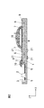
- FIG. 1 shows a circuit module on which a semiconductor chip having a control circuit or the like is mounted
- FIG. 2 shows a mounting configuration of the circuit module obtained by cutting the semiconductor chip in FIG.
- the circuit module includes, for example, a first semiconductor chip 3 having a diaphragm 2 and a second semiconductor chip 4 having a control circuit on a printed board 1 made of a material in which glass fibers and a resin are laminated.
- the printed circuit board 1 and the first semiconductor chip 3 are assembled with a first adhesive 5, and the printed circuit board 1 and the second semiconductor chip 4 are assembled with a second adhesive 6.
- a conductor wiring 8 and a wiring pad 9 for the conductor wiring are formed, and the first semiconductor chip 3 and the second semiconductor chip 4 are connected via the wire 7, the conductor wiring 8, and the wiring pad 9.
- the second semiconductor chip 4 is connected to the conductor wiring 8 through the wire 7.
- a potting 10 is installed to protect the wire 7.
- thermosetting resin such as an epoxy resin or a polyurethane resin, or a thermoplastic resin such as polyimide or an acrylic resin
- a filler such as glass or mica can be mixed in the resin. it can.
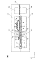
- circuit module mounting structure For the circuit module mounting structure described above, a manufacturing method for joining the circuit module and the housing while the area where the semiconductor component is mounted is exposed will be described.
- FIG. 3 shows a mold structure for molding a circuit module while exposing a region where semiconductor components are mounted.
- the circuit module mounted on the mold provided with the upper mold 11 and the lower mold 12 and the connector lead 13 are inserted, and the cavity portion 14 is formed by holding the circuit module with the clamp portion 15 of the mold. Resin 16 is filled.
- the circuit module wiring pads 9 and connector leads 13 are connected via wires 17. Further, in order to protect the circuit chamber 18 that is a space including the wires 17, an upper cover 19 and a lower cover 20 are joined to the upper and lower sides, respectively.
- a sensor module capable of joining the circuit module and the housing with the semiconductor components on the circuit module exposed and outputting a detection signal from the circuit module to the outside is completed.
- the upper mold 11 and the lower mold 12 are used to suppress the area where the circuit module member 21 is installed in the clamp portion 15, and the cavity portion 14 is filled with the resin 17 to form the housing. At the same time as forming, the circuit module and the housing are joined.
- the elastic modulus of the member 21 and the elastic modulus of the printed circuit board 1 are desirably compared at a temperature of 25 ° C. (room temperature).
- the elastic modulus can be compared between the elastic coefficient of the member 21 and the elastic coefficient of the base material constituting the printed circuit board 1.
- the hardness referred to here can be compared by, for example, any of Vickers hardness at room temperature, micro Vickers hardness, Brinell hardness, or Rockwell hardness.
- the member 21 can be made of a thermosetting resin such as an epoxy resin or a phenol resin, or a thermoplastic resin such as polycarbonate or polyethylene terephthalate, and the resin can be filled with glass or mica. Materials can also be mixed.
- a thermosetting resin such as an epoxy resin or a phenol resin
- a thermoplastic resin such as polycarbonate or polyethylene terephthalate
- Example 2 Next, the case where the wiring protection resist is arranged on the wiring in the printed circuit board 1 of the first embodiment will be described.
- the wiring 8 embedded in the printed circuit board 1 in FIG. 1 is formed on the substrate, and a wiring protection resist 23 is disposed to protect the wiring 8.
- the member 21 described above can also be applied to the configuration of the circuit board shown in FIG. In this case, it is possible to use the same material as the wiring protection resist 23 as long as the member 21 satisfies the condition that the elastic coefficient is lower than that of the circuit board. In this embodiment, since the member 21 can be installed at the same time as the installation process of the wiring protection resist 23, the process can be simplified.
- FIG. 8 shows a mounting configuration of the circuit module according to the third embodiment.
- a significant difference from the first and second embodiments is that a member 24 corresponding to the member 21 in the first and second embodiments is also added to the region of the joint 27 shown in FIGS.
- the third semiconductor chip 25 is connected to the wiring pad 9 through the outer leads 26 led out from the third semiconductor chip 25.
- insert molding is performed in order to join the circuit module and the housing with the region where the semiconductor component of the circuit module is mounted exposed.
- a member 24 is installed on the main surface of the circuit board 1 in an area where the circuit board 1 and the mold clamp portion 15 overlap and an area including the circuit board / resin joint 27.
- the thermal stress generated after molding due to the difference in the linear expansion coefficient between the circuit board 1 and the resin 16 can be alleviated by the installation of the member 21 to the joint portion 27, so that the distortion of the circuit board and the prevention of separation of the joint portion are possible. It is.
- Example 4 This embodiment is an embodiment in which the present invention is applied to a circuit board in which the conductor wiring 22 is also arranged in the clamp portion 15 and the joint portion 27.
- not only the wiring protection resist 23 is provided in the region other than the wiring pad 9 of the conductor wiring 22 and the region 28 where the conductor wiring is exposed.
- the conductor wiring 22 is also arranged in the portion 27.
- a member 24 is also disposed on the conductor wiring 22 disposed at the clamp portion 15 and the joint portion 27.
- insert molding is performed to join the circuit module and the housing while exposing the region 28 where the semiconductor components of the circuit module are mounted.
- the procedure for insert molding using a mold is the same as in Examples 1 to 3.
- the member 24 is arranged in a wide range as in the third embodiment, it is not necessary to arrange the member 24 with high accuracy in the region where the mold contacts, and the arrangement of the member 24 is the first and second embodiments. It is easier than Therefore, it is possible to improve yield deterioration.
- the thermal stress generated after molding due to the difference in linear expansion coefficient between the printed circuit board 1 and the resin 16 can be relaxed, and the distortion of the circuit board can be reduced and the separation of the joint portion can be prevented.
- the above is an example of a component in which an intake air amount sensor is insert-molded.
- the present invention is not limited to this, and can be used for any component in which a circuit board, particularly a printed board, is insert-molded. .
Landscapes
- Engineering & Computer Science (AREA)
- Microelectronics & Electronic Packaging (AREA)
- Physics & Mathematics (AREA)
- General Physics & Mathematics (AREA)
- Computer Hardware Design (AREA)
- Condensed Matter Physics & Semiconductors (AREA)
- Power Engineering (AREA)
- Fluid Mechanics (AREA)
- Manufacturing & Machinery (AREA)
- Geometry (AREA)
- Structures Or Materials For Encapsulating Or Coating Semiconductor Devices Or Solid State Devices (AREA)
- Encapsulation Of And Coatings For Semiconductor Or Solid State Devices (AREA)
- Injection Moulding Of Plastics Or The Like (AREA)
- Measuring Volume Flow (AREA)
Priority Applications (4)
| Application Number | Priority Date | Filing Date | Title |
|---|---|---|---|
| CN201580031470.7A CN106461439B (zh) | 2014-07-30 | 2015-06-15 | 传感器及其制造方法 |
| EP15827155.1A EP3176543B1 (de) | 2014-07-30 | 2015-06-15 | Leiterplattenmontagestruktur und sensor damit |
| US15/316,981 US10031006B2 (en) | 2014-07-30 | 2015-06-15 | Sensor including a printed circuit board with semiconductor parts having a first and second resin |
| JP2016538207A JP6357535B2 (ja) | 2014-07-30 | 2015-06-15 | センサおよびその製造方法 |
Applications Claiming Priority (2)
| Application Number | Priority Date | Filing Date | Title |
|---|---|---|---|
| JP2014-154430 | 2014-07-30 | ||
| JP2014154430 | 2014-07-30 |
Publications (1)
| Publication Number | Publication Date |
|---|---|
| WO2016017299A1 true WO2016017299A1 (ja) | 2016-02-04 |
Family
ID=55217204
Family Applications (1)
| Application Number | Title | Priority Date | Filing Date |
|---|---|---|---|
| PCT/JP2015/067110 WO2016017299A1 (ja) | 2014-07-30 | 2015-06-15 | 回路基板の実装構造、それを用いたセンサ |
Country Status (5)
| Country | Link |
|---|---|
| US (1) | US10031006B2 (de) |
| EP (1) | EP3176543B1 (de) |
| JP (1) | JP6357535B2 (de) |
| CN (1) | CN106461439B (de) |
| WO (1) | WO2016017299A1 (de) |
Cited By (4)
| Publication number | Priority date | Publication date | Assignee | Title |
|---|---|---|---|---|
| WO2017056572A1 (ja) * | 2015-09-30 | 2017-04-06 | 日立オートモティブシステムズ株式会社 | 樹脂成形体およびセンサ装置 |
| JP2017150929A (ja) * | 2016-02-24 | 2017-08-31 | 日立オートモティブシステムズ株式会社 | 物理量検出装置 |
| WO2018088141A1 (ja) * | 2016-11-14 | 2018-05-17 | 日立オートモティブシステムズ株式会社 | 半導体モジュール |
| JP2019158444A (ja) * | 2018-03-09 | 2019-09-19 | オムロン株式会社 | 電子装置およびその製造方法 |
Families Citing this family (8)
| Publication number | Priority date | Publication date | Assignee | Title |
|---|---|---|---|---|
| US10264664B1 (en) | 2015-06-04 | 2019-04-16 | Vlt, Inc. | Method of electrically interconnecting circuit assemblies |
| US10903734B1 (en) | 2016-04-05 | 2021-01-26 | Vicor Corporation | Delivering power to semiconductor loads |
| US11336167B1 (en) | 2016-04-05 | 2022-05-17 | Vicor Corporation | Delivering power to semiconductor loads |
| US10158357B1 (en) | 2016-04-05 | 2018-12-18 | Vlt, Inc. | Method and apparatus for delivering power to semiconductors |
| US10785871B1 (en) * | 2018-12-12 | 2020-09-22 | Vlt, Inc. | Panel molded electronic assemblies with integral terminals |
| JP6915160B2 (ja) * | 2018-05-22 | 2021-08-04 | 日立Astemo株式会社 | 物理量検出装置 |
| DE102020211142B4 (de) * | 2020-09-03 | 2022-08-18 | Vitesco Technologies GmbH | Gassensor für ein Fahrzeug |
| CN112802776B (zh) * | 2020-12-31 | 2023-10-20 | 苏州首肯机械有限公司 | 伺服半导体封装压机智能化压力控制系统及控制方法 |
Citations (3)
| Publication number | Priority date | Publication date | Assignee | Title |
|---|---|---|---|---|
| JP2001012987A (ja) * | 1999-06-30 | 2001-01-19 | Hitachi Ltd | 熱式空気流量センサ |
| JP2007033411A (ja) * | 2005-07-29 | 2007-02-08 | Denso Corp | センサ装置の製造方法及びセンサ装置 |
| JP2010169460A (ja) * | 2009-01-21 | 2010-08-05 | Denso Corp | 流量式センサ |
Family Cites Families (19)
| Publication number | Priority date | Publication date | Assignee | Title |
|---|---|---|---|---|
| JPH08236560A (ja) * | 1995-03-01 | 1996-09-13 | Hitachi Ltd | 半導体集積回路装置およびその製造方法 |
| JP4017480B2 (ja) * | 2002-09-24 | 2007-12-05 | Towa株式会社 | 樹脂封止金型 |
| JP2006211468A (ja) * | 2005-01-31 | 2006-08-10 | Sanyo Electric Co Ltd | 半導体センサ |
| JP4548199B2 (ja) * | 2005-04-22 | 2010-09-22 | 株式会社デンソー | 電子回路装置の製造方法 |
| JP4674529B2 (ja) * | 2005-11-07 | 2011-04-20 | 株式会社デンソー | 湿度センサ装置及びその製造方法 |
| JP4882732B2 (ja) * | 2006-12-22 | 2012-02-22 | 株式会社デンソー | 半導体装置 |
| ITMI20072099A1 (it) * | 2007-10-30 | 2009-04-30 | St Microelectronics Srl | Metodo di fabbricazione di un dispositivo elettronico comprendente dispositivi mems incapsulati per stampaggio |
| JP5068150B2 (ja) * | 2007-11-30 | 2012-11-07 | ジヤトコ株式会社 | 電気的解析の可能な制御基板ユニット |
| JP5208099B2 (ja) * | 2009-12-11 | 2013-06-12 | 日立オートモティブシステムズ株式会社 | 流量センサとその製造方法、及び流量センサモジュール |
| JP5563917B2 (ja) * | 2010-07-22 | 2014-07-30 | セミコンダクター・コンポーネンツ・インダストリーズ・リミテッド・ライアビリティ・カンパニー | 回路装置及びその製造方法 |
| WO2012049742A1 (ja) * | 2010-10-13 | 2012-04-19 | 日立オートモティブシステムズ株式会社 | 流量センサおよびその製造方法並びに流量センサモジュールおよびその製造方法 |
| JP5645693B2 (ja) | 2011-02-09 | 2014-12-24 | 日立オートモティブシステムズ株式会社 | 空気流量測定装置 |
| JP5526065B2 (ja) * | 2011-03-25 | 2014-06-18 | 日立オートモティブシステムズ株式会社 | 熱式センサおよびその製造方法 |
| WO2013008273A1 (ja) * | 2011-07-13 | 2013-01-17 | 日立オートモティブシステムズ株式会社 | 流量計 |
| JP2013188997A (ja) * | 2012-03-15 | 2013-09-26 | Toyota Motor Corp | 樹脂封止部品の製造方法 |
| JP5965706B2 (ja) * | 2012-04-12 | 2016-08-10 | 日立オートモティブシステムズ株式会社 | 流量センサの製造方法 |
| JP5675716B2 (ja) * | 2012-06-29 | 2015-02-25 | 日立オートモティブシステムズ株式会社 | 熱式空気流量センサ |
| JP6018903B2 (ja) * | 2012-12-17 | 2016-11-02 | 日立オートモティブシステムズ株式会社 | 物理量センサ |
| JP5949667B2 (ja) * | 2013-06-03 | 2016-07-13 | 株式会社デンソー | モールドパッケージおよびその製造方法 |
-
2015
- 2015-06-15 CN CN201580031470.7A patent/CN106461439B/zh active Active
- 2015-06-15 US US15/316,981 patent/US10031006B2/en active Active
- 2015-06-15 EP EP15827155.1A patent/EP3176543B1/de active Active
- 2015-06-15 WO PCT/JP2015/067110 patent/WO2016017299A1/ja active Application Filing
- 2015-06-15 JP JP2016538207A patent/JP6357535B2/ja active Active
Patent Citations (3)
| Publication number | Priority date | Publication date | Assignee | Title |
|---|---|---|---|---|
| JP2001012987A (ja) * | 1999-06-30 | 2001-01-19 | Hitachi Ltd | 熱式空気流量センサ |
| JP2007033411A (ja) * | 2005-07-29 | 2007-02-08 | Denso Corp | センサ装置の製造方法及びセンサ装置 |
| JP2010169460A (ja) * | 2009-01-21 | 2010-08-05 | Denso Corp | 流量式センサ |
Non-Patent Citations (1)
| Title |
|---|
| See also references of EP3176543A4 * |
Cited By (8)
| Publication number | Priority date | Publication date | Assignee | Title |
|---|---|---|---|---|
| WO2017056572A1 (ja) * | 2015-09-30 | 2017-04-06 | 日立オートモティブシステムズ株式会社 | 樹脂成形体およびセンサ装置 |
| JPWO2017056572A1 (ja) * | 2015-09-30 | 2018-02-08 | 日立オートモティブシステムズ株式会社 | 樹脂成形体およびセンサ装置 |
| US10217684B2 (en) | 2015-09-30 | 2019-02-26 | Hitachi Automotive Systems, Ltd. | Resin molding and sensor device |
| JP2017150929A (ja) * | 2016-02-24 | 2017-08-31 | 日立オートモティブシステムズ株式会社 | 物理量検出装置 |
| WO2018088141A1 (ja) * | 2016-11-14 | 2018-05-17 | 日立オートモティブシステムズ株式会社 | 半導体モジュール |
| JP2018081959A (ja) * | 2016-11-14 | 2018-05-24 | 日立オートモティブシステムズ株式会社 | 半導体モジュール |
| US10644423B2 (en) | 2016-11-14 | 2020-05-05 | Hitachi Automotive Systems, Ltd. | Semiconductor module |
| JP2019158444A (ja) * | 2018-03-09 | 2019-09-19 | オムロン株式会社 | 電子装置およびその製造方法 |
Also Published As
| Publication number | Publication date |
|---|---|
| EP3176543B1 (de) | 2020-11-18 |
| EP3176543A1 (de) | 2017-06-07 |
| US20170115144A1 (en) | 2017-04-27 |
| JP6357535B2 (ja) | 2018-07-11 |
| JPWO2016017299A1 (ja) | 2017-04-27 |
| CN106461439B (zh) | 2019-08-16 |
| US10031006B2 (en) | 2018-07-24 |
| CN106461439A (zh) | 2017-02-22 |
| EP3176543A4 (de) | 2018-03-21 |
Similar Documents
| Publication | Publication Date | Title |
|---|---|---|
| JP6357535B2 (ja) | センサおよびその製造方法 | |
| JP4281630B2 (ja) | センサ装置の製造方法 | |
| JP5450192B2 (ja) | パワーモジュールとその製造方法 | |
| JP2009058230A (ja) | センサ装置の製造方法及びセンサ装置 | |
| US10217684B2 (en) | Resin molding and sensor device | |
| JP5763575B2 (ja) | 流量センサおよびその製造方法 | |
| JP2010096614A (ja) | センサ装置 | |
| JP5494403B2 (ja) | センサ装置およびその製造方法 | |
| JP6373104B2 (ja) | 半導体圧力センサ及び半導体圧力センサ取付構造体 | |
| WO2016039019A1 (ja) | 流量センサ | |
| JP2014009974A (ja) | 流量測定装置 | |
| JP6045644B2 (ja) | 流量センサおよびその製造方法 | |
| WO2014136336A1 (ja) | センサ装置 | |
| JP6370379B2 (ja) | 半導体装置、該半導体装置の製造方法及び該半導体装置を用いたセンサ | |
| JP2015227892A (ja) | 流量測定装置 | |
| JP6012833B2 (ja) | 半導体装置およびその製造方法並びに流量センサおよび湿度センサ | |
| JP2014126507A (ja) | 圧力センサモジュール | |
| JP5912069B2 (ja) | 物理量センサ装置及びその製造方法 | |
| JP2014006210A (ja) | 流量センサおよびその製造方法 | |
| JP6658104B2 (ja) | 回路装置 | |
| WO2018123478A1 (ja) | センサ装置及びその製造方法 | |
| TW201810449A (zh) | 包含載體及殼體的裝置,以及製造包含構件的裝置的方法 |
Legal Events
| Date | Code | Title | Description |
|---|---|---|---|
| 121 | Ep: the epo has been informed by wipo that ep was designated in this application |
Ref document number: 15827155 Country of ref document: EP Kind code of ref document: A1 |
|
| ENP | Entry into the national phase |
Ref document number: 2016538207 Country of ref document: JP Kind code of ref document: A |
|
| REEP | Request for entry into the european phase |
Ref document number: 2015827155 Country of ref document: EP |
|
| WWE | Wipo information: entry into national phase |
Ref document number: 2015827155 Country of ref document: EP |
|
| WWE | Wipo information: entry into national phase |
Ref document number: 15316981 Country of ref document: US |
|
| NENP | Non-entry into the national phase |
Ref country code: DE |