WO2016010094A1 - 発光装置 - Google Patents
発光装置 Download PDFInfo
- Publication number
- WO2016010094A1 WO2016010094A1 PCT/JP2015/070319 JP2015070319W WO2016010094A1 WO 2016010094 A1 WO2016010094 A1 WO 2016010094A1 JP 2015070319 W JP2015070319 W JP 2015070319W WO 2016010094 A1 WO2016010094 A1 WO 2016010094A1
- Authority
- WO
- WIPO (PCT)
- Prior art keywords
- light emitting
- emitting unit
- outer peripheral
- central
- emitting device
- Prior art date
- Legal status (The legal status is an assumption and is not a legal conclusion. Google has not performed a legal analysis and makes no representation as to the accuracy of the status listed.)
- Ceased
Links
Images








Classifications
-
- F—MECHANICAL ENGINEERING; LIGHTING; HEATING; WEAPONS; BLASTING
- F21—LIGHTING
- F21K—NON-ELECTRIC LIGHT SOURCES USING LUMINESCENCE; LIGHT SOURCES USING ELECTROCHEMILUMINESCENCE; LIGHT SOURCES USING CHARGES OF COMBUSTIBLE MATERIAL; LIGHT SOURCES USING SEMICONDUCTOR DEVICES AS LIGHT-GENERATING ELEMENTS; LIGHT SOURCES NOT OTHERWISE PROVIDED FOR
- F21K9/00—Light sources using semiconductor devices as light-generating elements, e.g. using light-emitting diodes [LED] or lasers
-
- F—MECHANICAL ENGINEERING; LIGHTING; HEATING; WEAPONS; BLASTING
- F21—LIGHTING
- F21S—NON-PORTABLE LIGHTING DEVICES; SYSTEMS THEREOF; VEHICLE LIGHTING DEVICES SPECIALLY ADAPTED FOR VEHICLE EXTERIORS
- F21S2/00—Systems of lighting devices, not provided for in main groups F21S4/00 - F21S10/00 or F21S19/00, e.g. of modular construction
- F21S2/005—Systems of lighting devices, not provided for in main groups F21S4/00 - F21S10/00 or F21S19/00, e.g. of modular construction of modular construction
-
- F—MECHANICAL ENGINEERING; LIGHTING; HEATING; WEAPONS; BLASTING
- F21—LIGHTING
- F21V—FUNCTIONAL FEATURES OR DETAILS OF LIGHTING DEVICES OR SYSTEMS THEREOF; STRUCTURAL COMBINATIONS OF LIGHTING DEVICES WITH OTHER ARTICLES, NOT OTHERWISE PROVIDED FOR
- F21V19/00—Fastening of light sources or lamp holders
- F21V19/001—Fastening of light sources or lamp holders the light sources being semiconductors devices, e.g. LEDs
- F21V19/0015—Fastening arrangements intended to retain light sources
- F21V19/002—Fastening arrangements intended to retain light sources the fastening means engaging the encapsulation or the packaging of the semiconductor device
-
- F—MECHANICAL ENGINEERING; LIGHTING; HEATING; WEAPONS; BLASTING
- F21—LIGHTING
- F21V—FUNCTIONAL FEATURES OR DETAILS OF LIGHTING DEVICES OR SYSTEMS THEREOF; STRUCTURAL COMBINATIONS OF LIGHTING DEVICES WITH OTHER ARTICLES, NOT OTHERWISE PROVIDED FOR
- F21V23/00—Arrangement of electric circuit elements in or on lighting devices
- F21V23/06—Arrangement of electric circuit elements in or on lighting devices the elements being coupling devices, e.g. connectors
-
- F—MECHANICAL ENGINEERING; LIGHTING; HEATING; WEAPONS; BLASTING
- F21—LIGHTING
- F21V—FUNCTIONAL FEATURES OR DETAILS OF LIGHTING DEVICES OR SYSTEMS THEREOF; STRUCTURAL COMBINATIONS OF LIGHTING DEVICES WITH OTHER ARTICLES, NOT OTHERWISE PROVIDED FOR
- F21V29/00—Protecting lighting devices from thermal damage; Cooling or heating arrangements specially adapted for lighting devices or systems
- F21V29/85—Protecting lighting devices from thermal damage; Cooling or heating arrangements specially adapted for lighting devices or systems characterised by the material
- F21V29/89—Metals
-
- F—MECHANICAL ENGINEERING; LIGHTING; HEATING; WEAPONS; BLASTING
- F21—LIGHTING
- F21Y—INDEXING SCHEME ASSOCIATED WITH SUBCLASSES F21K, F21L, F21S and F21V, RELATING TO THE FORM OR THE KIND OF THE LIGHT SOURCES OR OF THE COLOUR OF THE LIGHT EMITTED
- F21Y2105/00—Planar light sources
- F21Y2105/10—Planar light sources comprising a two-dimensional [2D] array of point-like light-generating elements
- F21Y2105/14—Planar light sources comprising a two-dimensional [2D] array of point-like light-generating elements characterised by the overall shape of the two-dimensional [2D] array
- F21Y2105/18—Planar light sources comprising a two-dimensional [2D] array of point-like light-generating elements characterised by the overall shape of the two-dimensional [2D] array annular; polygonal other than square or rectangular, e.g. for spotlights or for generating an axially symmetrical light beam
-
- F—MECHANICAL ENGINEERING; LIGHTING; HEATING; WEAPONS; BLASTING
- F21—LIGHTING
- F21Y—INDEXING SCHEME ASSOCIATED WITH SUBCLASSES F21K, F21L, F21S and F21V, RELATING TO THE FORM OR THE KIND OF THE LIGHT SOURCES OR OF THE COLOUR OF THE LIGHT EMITTED
- F21Y2107/00—Light sources with three-dimensionally disposed light-generating elements
- F21Y2107/50—Light sources with three-dimensionally disposed light-generating elements on planar substrates or supports, but arranged in different planes or with differing orientation, e.g. on plate-shaped supports with steps on which light-generating elements are mounted
-
- F—MECHANICAL ENGINEERING; LIGHTING; HEATING; WEAPONS; BLASTING
- F21—LIGHTING
- F21Y—INDEXING SCHEME ASSOCIATED WITH SUBCLASSES F21K, F21L, F21S and F21V, RELATING TO THE FORM OR THE KIND OF THE LIGHT SOURCES OR OF THE COLOUR OF THE LIGHT EMITTED
- F21Y2107/00—Light sources with three-dimensionally disposed light-generating elements
- F21Y2107/60—Light sources with three-dimensionally disposed light-generating elements on stacked substrates
-
- F—MECHANICAL ENGINEERING; LIGHTING; HEATING; WEAPONS; BLASTING
- F21—LIGHTING
- F21Y—INDEXING SCHEME ASSOCIATED WITH SUBCLASSES F21K, F21L, F21S and F21V, RELATING TO THE FORM OR THE KIND OF THE LIGHT SOURCES OR OF THE COLOUR OF THE LIGHT EMITTED
- F21Y2113/00—Combination of light sources
- F21Y2113/10—Combination of light sources of different colours
- F21Y2113/13—Combination of light sources of different colours comprising an assembly of point-like light sources
-
- F—MECHANICAL ENGINEERING; LIGHTING; HEATING; WEAPONS; BLASTING
- F21—LIGHTING
- F21Y—INDEXING SCHEME ASSOCIATED WITH SUBCLASSES F21K, F21L, F21S and F21V, RELATING TO THE FORM OR THE KIND OF THE LIGHT SOURCES OR OF THE COLOUR OF THE LIGHT EMITTED
- F21Y2115/00—Light-generating elements of semiconductor light sources
- F21Y2115/10—Light-emitting diodes [LED]
-
- H—ELECTRICITY
- H10—SEMICONDUCTOR DEVICES; ELECTRIC SOLID-STATE DEVICES NOT OTHERWISE PROVIDED FOR
- H10W—GENERIC PACKAGES, INTERCONNECTIONS, CONNECTORS OR OTHER CONSTRUCTIONAL DETAILS OF DEVICES COVERED BY CLASS H10
- H10W90/00—Package configurations
Definitions
- the present invention relates to a light emitting device.
- Patent Document 1 includes a strip-shaped LED board and a plurality of LEDs arranged along the array line of the LED board, and a connector at a position off the array line at the end of the LED board. The lighting fixture using the provided LED unit is described.
- Patent Document 1 it is described that a plurality of LED units curved in a partial arc shape are connected to each other to form an annular light emitting region. A plate-shaped light emitting region is not formed.
- an object of the present invention is to provide a light-emitting device in which the light-emitting area is enlarged without increasing the yield and the amount of light in the central portion is increased as compared with the case without the present configuration.
- the plurality of outer peripheral light emitting units include those having different emission colors.
- the plurality of outer peripheral light emitting units having different emission colors are connected in parallel to an external power source.
- each of the central light emitting unit and the plurality of outer peripheral light emitting units has a sealing resin that seals the light emitting element and a resin frame that fixes the sealing resin, and the light emitting region of the central light emitting unit is the central light emitting unit. It is an area covered with the sealing resin of the unit, and the light emitting area of the outer peripheral light emitting unit is preferably an area covered with the sealing resin of the outer peripheral light emitting unit.
- the resin frames of the plurality of outer peripheral light emitting units are not provided at the end portion facing the adjacent outer peripheral light emitting unit.
- the resin frames of the plurality of outer peripheral light-emitting units are not provided at the end facing the central light-emitting unit.
- the sealing resin of the central light emitting unit has a disk shape, and the sealing resin in a region where the central light emitting unit and the plurality of outer peripheral light emitting units are completely filled also has a disk shape as a whole.
- each of the central light emitting unit and the plurality of outer peripheral light emitting units preferably has a ceramic circuit board as a substrate.
- the light emitting elements of the central light emitting unit and the light emitting elements of the plurality of outer peripheral light emitting units are mounted on the substrate at relatively different heights.
- the light emitting area can be enlarged and the amount of light in the central portion can be increased without deteriorating the yield as compared with the case without this configuration.
- FIG. 1 is an exploded view of a light emitting device 1.
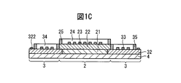
- FIG. 2 is a cross-sectional view of the light emitting device 1 taken along the line IC-IC.
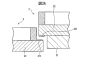
- FIG. 3 is an enlarged partial cross-sectional view showing a connection portion between a central light emitting unit 2 and an outer peripheral light emitting unit 3.
- FIG. 3 is an enlarged partial cross-sectional view showing a connection portion between a central light emitting unit 2 and an outer peripheral light emitting unit 3.
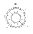
- FIG. It is a top view of the light emitting device 1A. It is an exploded view of 1 A of light-emitting devices.
- FIG. 3 is a sectional view of the light emitting device 1A taken along line IIIC-IIIC.
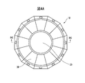
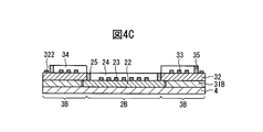
- FIG. 4 is a sectional view of the light emitting device 1B taken along line IVC-IVC. It is sectional drawing of 1 C of light-emitting devices. It is sectional drawing of light-emitting device 1D. It is sectional drawing of the light-emitting device 1E. It is sectional drawing of the light-emitting device 1F.
- 1A to 1C are a top view, an exploded view, and a cross-sectional view taken along line IA-IA of the light emitting device 1, respectively.
- 2A and 2B are enlarged partial cross-sectional views showing a connection portion between the central light emitting unit 2 and the outer peripheral light emitting unit 3.
- a light emitting device 1 includes a central light emitting unit 2 disposed at the center of the device, and a plurality of outer peripheral light emitting units 3 disposed along the outer shape so as to surround the central light emitting unit 2. And have.
- the plurality of outer peripheral light emitting units 3 are arranged so as to fill the outer periphery of the central light emitting unit 2. These light emitting units are connected to each other to form one large light emitting region. That is, the light emitting device 1 realizes an enlargement of the light emitting region by connecting a plurality of light emitting units that can be connected to each other.
- the number of outer peripheral light emitting units 3 may be any number, and FIGS. 1A to 1C show an example in which there are twelve outer peripheral light emitting units 3.
- the light emitting device 1 has a regular dodecagonal metal heat dissipation substrate 4.
- the central light emitting unit 2 and the twelve outer peripheral light emitting units 3 are disposed on the heat dissipation substrate 4.
- the heat dissipation board 4 is made of an aluminum material having excellent heat resistance and heat dissipation.
- the heat dissipation substrate 4 is not shown in FIGS. 1A and 1B.
- the central light emitting unit 2 includes a heat dissipation board 21, a circuit board 22, an LED element 23, a sealing resin 24, and a resin frame 25 as main components.
- the heat dissipation substrate 21 is a metal substrate made of an aluminum material having excellent heat resistance and heat dissipation, similar to the heat dissipation substrate 4.
- the heat dissipation substrate 21 has a disk shape and is fixed to the center of the heat dissipation substrate 4 as shown in FIG. 1C. Accordingly, in the light emitting device 1, the central light emitting unit 2 is arranged at a higher position than the outer peripheral light emitting unit 3.
- the heat dissipation substrate 21 efficiently dissipates heat generated by the LED elements 23.
- the circuit board 22 is, for example, an insulating substrate such as a glass epoxy substrate or a ceramic substrate, and has a disk shape like the heat dissipation substrate 21.
- the circuit board 22 is attached and fixed to the upper surface of the heat dissipation board 21.
- a connection electrode 221 for electrically connecting the central light emitting unit 2 and each peripheral light emitting unit 3 is formed on the lower surface of the outer peripheral portion of the circuit board 22.
- twelve connection electrodes 221 corresponding to the number of the outer peripheral light emitting units 3 are arranged at equal intervals.
- a wiring pattern (not shown) is formed on the upper surface of the circuit board 22, and this wiring pattern is electrically connected to the connection electrode 221. Note that connection electrodes for directly connecting the central light emitting unit 2 to an external power source may be formed on the circuit board 22.
- the LED element 23 is an example of a light emitting element.
- a plurality of LED elements 23 are arranged on the upper surface of the circuit board 22 with a space between each other, and are fixed by a transparent insulating adhesive or the like.
- the LED element 23 has a pair of element electrodes on the upper surface, and the element electrodes of the adjacent LED elements 23 are connected to each other by a bonding wire (not shown). Bonding wires coming out of the LED elements 23 located on the outer peripheral side of the circuit board 22 are connected to the wiring pattern of the circuit board 22.
- the sealing resin 24 is a colorless and transparent resin such as an epoxy resin or a silicon resin, and integrally covers and protects the LED element 23.
- a region covered with the sealing resin 24 is a light emitting region of the central light emitting unit 2.
- the sealing resin 24 is molded into a disk shape and fixed on the circuit board 22 by the resin frame 25.
- the phosphor is dispersed and mixed in the sealing resin 24.
- the light emitting device 1 emits white light obtained by mixing blue light from the blue LED element, green light from the green LED element, and red light obtained by exciting the red phosphor with them. Exit.
- the resin frame 25 is a circular frame made of, for example, white resin, and fixes the sealing resin 24 on the circuit board 22.
- the resin frame 25 reflects light emitted laterally from the LED element 23 toward the upper side of the light emitting device 1 (the side opposite to the circuit board 22 when viewed from the LED element 23).
- Each peripheral light emitting unit 3 includes a circuit board 32, an LED element 33, a sealing resin 34, and a resin frame 35 as main components.
- the heat radiating substrate 4 functions as a heat radiating substrate for each outer peripheral light emitting unit 3.
- a substrate may be provided.
- the circuit board 32 is an insulating board such as a glass epoxy board or a ceramic board. As shown in FIG. 1A, the circuit board 32 has a substantially trapezoidal shape that is symmetrical with respect to the central axis so that a larger substantially circular region can be formed when twelve outer peripheral light emitting units 3 are arranged around the central light emitting unit 2. Has a shape. However, the shape of the circuit board 32 (outer peripheral light emitting unit 3) is shown in FIG. 1A as long as a substantially circular region larger than the central light emitting unit 2 is formed when a plurality of outer peripheral light emitting units 3 are connected. It is not limited to that.
- the circuit board 32 is attached and fixed to the upper surface of the heat dissipation board 4 around the central light emitting unit 2. As shown in FIGS. 2A and 2B, when the central light emitting unit 2 and the outer peripheral light emitting unit 3 are joined together, near the end of the circuit board 32 on the side in contact with the central light emitting unit 2 (hereinafter referred to as “inner peripheral side”) The connection electrode 321 is formed. In the light emitting device 1, the circuit board 22 is higher than the circuit board 32 by the thickness of the heat dissipation board 21 of the central light emitting unit 2.
- connection electrode 221 on the lower surface of the circuit board 22 and the connection electrode 321 on the upper surface of the circuit board 32 are in contact, and the central light emitting unit is connected at the joint between the substrates. 2 and the outer peripheral light emitting unit 3 are electrically connected.
- connection electrode 322 is formed in the vicinity of the end of the circuit board 32 that becomes the outer side (outer peripheral side) of the light emitting device 1 when the central light emitting unit 2 and the outer peripheral light emitting unit 3 are joined together.
- Each outer peripheral light emitting unit 3 is connected to an external power source via a connection electrode 322.
- a wiring pattern (not shown) that is electrically connected to the connection electrode 321 or the connection electrode 322 is formed on the upper surface of the circuit board 32.
- the LED element 33 is an example of a light-emitting element.
- a plurality of LED elements 33 are arranged on the upper surface of the circuit board 32 with a space between each other. It is fixed with adhesive.
- the element electrode of each LED element 33 is connected to the adjacent LED element 33 or the wiring pattern of the circuit board 32 by a bonding wire (not shown).
- the sealing resin 34 is a colorless and transparent resin such as an epoxy resin or a silicon resin, like the sealing resin 24, and integrally covers and protects the LED element 33.
- a region covered with the sealing resin 34 is a light emitting region of the outer peripheral light emitting unit 3.
- the sealing resin 34 is molded according to the shape of the circuit board 32 and is fixed on the circuit board 32 by the resin frame 35.
- the phosphor is also dispersed and mixed in the sealing resin 34.
- the resin frame 35 is a frame body made of, for example, white resin in accordance with the shape of the sealing resin 34, and fixes the sealing resin 34 on the circuit board 32. Similar to the resin frame 25, the resin frame 35 reflects the light emitted from the LED elements 33 to the upper side of the light emitting device 1. As shown in FIGS. 1A and 1B, in the outer peripheral light emitting unit 3 of the light emitting device 1, the entire outer periphery of the sealing resin 34 is surrounded by a resin frame 35.
- the sealing resin 24 of the central light emitting unit 2 has a disk shape, and the sealing resin 24 in a region where the central light emitting unit 2 and the plurality of outer peripheral light emitting units 3 are filled up, 34 also has a disk shape as a whole.
- the shape of the light emitting region is preferably circular considering that the light emitting device is used in an actual lighting fixture or the like. For example, since many reflectors of lighting fixtures are made on the assumption of a circular light emitting region, the reflection efficiency at the reflector is improved when the shape of the light emitting region is as close to a circle as possible.
- the resin region of the central light emitting unit 2 and the resin region of the light emitting device 1 as a whole may be a polygon that is close to a circle such as a hexagon or an octagon, and may not necessarily be a perfect circle.
- the resin area of one outer peripheral light emitting unit 3 is smaller than the resin area of the central light emitting unit 2. This is because in the illumination application, it is necessary to brighten the central portion serving as the optical axis, and therefore it is preferable to manufacture the central light emitting unit 2 as large as possible within the range in which the quality is guaranteed. If the area of the central light emitting unit 2 is maximized within the range in which quality is guaranteed, the area of each outer peripheral light emitting unit 3 is equal to or smaller than the area of the central light emitting unit 2. Therefore, it is preferable that the sealing resin 34 of each outer peripheral light emitting unit 3 has an area equal to or smaller than the sealing resin 24 of the central light emitting unit 2.
- the plurality of outer peripheral light emitting units 3 may include ones having different emission colors.
- one light emitting device may include devices having different colors such as the outer peripheral light emitting unit 3 having a color temperature of 4000K and the outer peripheral light emitting unit 3 having a color temperature of 4000K.
- the type and composition (combination) of phosphors mixed in the sealing resin 34 of the outer peripheral light emitting unit 3 are changed, or blue LED elements that emit blue light and green LED elements that emit green light.
- the ratio of the numbers may be changed for each outer peripheral light emitting unit 3.
- the outer peripheral light emitting units 3 of all colors are caused to emit light.
- These lights can be mixed in color, or only the outer peripheral light emitting unit 3 of a certain color can emit light. In this way, in the light emitting device 1, it is possible to freely adjust the color tone and the light amount as a whole according to the application, thereby improving the color rendering.
- the light emitting device 1A includes a central light emitting unit 2A, a plurality of outer peripheral light emitting units 3A arranged around the central light emitting unit 2A, and a heat dissipation substrate 4.
- the configuration of the light emitting device 1A is the same as the configuration of the light emitting device 1 shown in FIGS. 1A to 1C except for the shape of the resin frame 35A of the outer peripheral light emitting unit 3A. For this reason, the same code
- the resin frame 35A of each outer peripheral light emitting unit 3A is connected to the adjacent outer peripheral light emitting unit 3A when the central light emitting unit 2A and the plurality of outer peripheral light emitting units 3A are joined together. It is not provided at the facing side end 351. Thereby, in the light emitting device 1A, compared with the light emitting device 1, the area covered with the sealing resin 34 is widened by the side end portion 351, so that the area of the light emitting region is increased.
- the light emission colors from the plurality of outer peripheral light emitting units 3A are likely to be mixed as compared with the light emitting device 1. Since the color mixing state can be changed depending on the presence or absence of the resin frame, in the light emitting device 1A, the color rendering properties can be further improved by appropriately adjusting the light emission color of each outer peripheral light emitting unit 3A.
- the light emitting device 1B includes a central light emitting unit 2B, a plurality of outer peripheral light emitting units 3B arranged around the central light emitting unit 2B, and a heat dissipation substrate 4.
- the configuration of the light emitting device 1B is that the central light emitting unit 2B has no heat dissipation substrate, the outer peripheral light emitting unit 3B has a heat dissipation substrate 31B at the bottom, and the shape of the resin frame 35B of the outer peripheral light emitting unit 3B is different.
- the configuration is the same as that of the light emitting device 1 shown in FIGS. 1A to 1C. For this reason, the same code
- the resin frame 35B of each outer peripheral light emitting unit 3B faces not only the side end facing the adjacent outer peripheral light emitting unit 3B but also the central light emitting unit 2B. It is not provided on the inner peripheral side end 352. Thereby, in the light emitting device 1B, the area of the light emitting region is further increased by the inner peripheral side end portion 352, and the light emission colors from the central light emitting unit 2B and the plurality of outer peripheral light emitting units 3B are larger than the light emitting device 1A. Furthermore, it becomes easy to mix colors.
- the circuit board 32 is positioned higher than the circuit board 22 by the thickness of the heat dissipation board 31B of the outer peripheral light emitting unit 3B. It is in.
- the light emitting device 1B since there is no resin frame 35B at the inner peripheral side end 352 of the outer peripheral light emitting unit 3B, if the height of the central light emitting unit 2B is lowered, the light from each outer peripheral light emitting unit 3B is transmitted to the central light emitting unit 2B. Toward the horizontal direction. Therefore, also in this respect, in the light emitting device 1B, compared with the light emitting device 1A, the light emission colors from the respective light emitting units are more easily mixed.
- the LED elements 23 of the central light emitting units 2, 2A, 2B and the LED elements 33 of the plurality of outer peripheral light emitting units 3, 3A, 3B are arranged at relatively different heights. 22 and 32 may be mounted. Alternatively, all the LED elements 23 and 33 may be mounted at the same height. Further, depending on the application, the outer peripheral light emitting unit 3 having a resin frame on all sides, the outer peripheral light emitting unit 3A having no resin frame at the side end 351, and the outer peripheral light emitting unit having no resin frame at the inner peripheral end 352. Two or all of 3B may be mixed in one light-emitting device.
- the resin frame 25 may be removed or the resin frame 25 may be provided only on a part of the outer periphery of the sealing resin 24.
- the resin frame 25 may be provided only on a part of the outer periphery of the sealing resin 24.
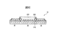
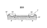
- 5A to 5D are cross-sectional views of the light emitting devices 1C to 1F, respectively.
- a longitudinal section passing through the center of each light emitting device is shown. Since the light-emitting devices 1C to 1F have the same configuration as the light-emitting devices 1, 1A, and 1B that have already been described, redundant descriptions are omitted.
- the light emitting device 1C shown in FIG. 5A is the same light emitting device as the light emitting devices 1 and 1A.
- the circuit board 22C of the central light emitting unit 2C and the circuit board 32C of each outer peripheral light emitting unit 3C are through holes 222, respectively. , 323, and the LED element is mounted directly on the heat dissipation boards 21C, 4.
- 5B is a light emitting device similar to the light emitting device 1B.
- the circuit board 22D of the central light emitting unit 2D and the circuit board 32D of each outer peripheral light emitting unit 3D are each through-holes 222. , 323, and the LED element is mounted directly on the heat dissipation substrate 4, 31D. In this way, each LED element may be directly mounted on a metal heat dissipation board to further improve heat dissipation.
- the light emitting device 1E shown in FIG. 5C is the same light emitting device as the light emitting devices 1 and 1A. However, in the light emitting device 1E, only the circuit board 22E of the central light emitting unit 2E has the through hole 222, and the LED of the central light emitting unit 2E The element is directly mounted on the heat dissipation board 21E.
- 5D is a light emitting device similar to the light emitting device 1B. However, in the light emitting device 1F, only the circuit board 32F of each outer peripheral light emitting unit 3F has a through-hole 323, and the outer peripheral light emitting unit 3F has a through hole 323. The LED element is directly mounted on the heat dissipation board 31F.
- a light emitting unit having a through hole in the circuit board and a light emitting unit having no through hole may be mixed.
- an LED element that generates a relatively large amount of heat is disposed in a light emitting unit that has a through hole
- an LED element that generates a relatively small amount of heat is disposed in a light emitting unit that does not have a through hole. It is preferable.
- a circuit board having a through hole and a circuit board having no through hole may be mixed.
- one large substantially circular (disc) is formed by a central light emitting unit disposed at the center of the device and a plurality of outer peripheral light emitting units disposed along the outer shape so as to surround the central light emitting unit.
- Shape) light emitting region is formed. That is, in these light-emitting devices, by connecting together a plurality of light-emitting units that can be connected to each other, it is possible to increase the size of the light-emitting region and increase the amount of light in the central portion without deteriorating the yield.
- Such a light-emitting device allows various module configurations as a light-emitting device by changing the number, shape, connection method, and the like of the outer peripheral light-emitting units to be combined.
- the entire circuit can be configured by freely combining them in parallel or in series. At this time, if the number of light emitting units connected in series is increased, it is possible to suppress variations in luminous intensity due to variations in forward voltage (forward voltage, VF) of LED elements included in each light emitting unit.
- forward voltage forward voltage
- the color of emitted light can be changed for each light emitting unit, so that the color rendering can be improved. Since a plurality of light emitting regions having a relatively small area are combined, variation in the light emission color that can occur when one light emitting region is enlarged is suppressed, and chromaticity defects can be reduced. In addition, although the sink becomes more likely to occur as the area of the resin region becomes larger, in the above light emitting device, since a plurality of light emitting regions having a smaller area are combined, occurrence of upper surface sink on the sealing resin in each light emitting unit is suppressed. Can do.
- the circuit board is easily broken by the heat generation of the LED element when the area is increased.
- the circuit board since the area of each light-emitting unit is relatively small, there is an advantage that the circuit board is hardly broken even when a ceramic substrate is used.
- the outer peripheral light emitting units are arranged so as to surround the central light emitting unit in a single layer, but the outer peripheral light emitting units are arranged in a double and triple manner around the central light emitting unit, It is also possible to form a larger light emitting region.
Landscapes
- Engineering & Computer Science (AREA)
- General Engineering & Computer Science (AREA)
- Physics & Mathematics (AREA)
- Microelectronics & Electronic Packaging (AREA)
- Optics & Photonics (AREA)
- Led Device Packages (AREA)
- Fastening Of Light Sources Or Lamp Holders (AREA)
- Non-Portable Lighting Devices Or Systems Thereof (AREA)
Abstract
Description
上記の発光装置では、発光色が異なる複数の外周発光ユニットは、外部電源に並列に接続されることが好ましい。
上記の発光装置では、複数の外周発光ユニットの樹脂枠は、隣接する外周発光ユニットに面した端部には設けられていないことが好ましい。
上記の発光装置では、複数の外周発光ユニットの樹脂枠は、中心発光ユニットに面した端部にも設けられていないことが好ましい。
上記の発光装置では、中心発光ユニットと複数の外周発光ユニットのそれぞれは、基板として、セラミックス製の回路基板を有することが好ましい。
上記の発光装置では、中心発光ユニットの発光素子と複数の外周発光ユニットの発光素子とは、相対的に異なる高さで基板上に実装されることが好ましい。
Claims (9)
- 中心発光ユニットと、
前記中心発光ユニットの外周を埋め尽くすように配置された複数の外周発光ユニットと、を有し、
前記中心発光ユニットと前記複数の外周発光ユニットのそれぞれは、基板および前記基板上に実装された発光素子を有し、
個々の前記外周発光ユニットの発光領域の面積は、前記中心発光ユニットの発光領域の面積以下である、
ことを特徴とする発光装置。 - 前記複数の外周発光ユニットには、発光色が異なるものが含まれる、請求項1に記載の発光装置。
- 前記発光色が異なる複数の外周発光ユニットは、外部電源に並列に接続される、請求項2に記載の発光装置。
- 前記中心発光ユニットと前記複数の外周発光ユニットのそれぞれは、前記発光素子を封止する封止樹脂および前記封止樹脂を固定する樹脂枠を有し、
前記中心発光ユニットの発光領域は前記中心発光ユニットの封止樹脂で覆われる領域であり、
前記外周発光ユニットの発光領域は前記外周発光ユニットの封止樹脂で覆われる領域である、請求項1~3のいずれか一項に記載の発光装置。 - 前記複数の外周発光ユニットの樹脂枠は、隣接する外周発光ユニットに面した端部には設けられていない、請求項4に記載の発光装置。
- 前記複数の外周発光ユニットの樹脂枠は、前記中心発光ユニットに面した端部にも設けられていない、請求項5に記載の発光装置。
- 前記中心発光ユニットの封止樹脂は円板形状を有し、前記中心発光ユニットと前記複数の外周発光ユニットが埋め尽くす領域の封止樹脂も全体として円板形状を有する、請求項4~6のいずれか一項に記載の発光装置。
- 前記中心発光ユニットと前記複数の外周発光ユニットのそれぞれは、前記基板として、セラミックス製の回路基板を有する、請求項1~7のいずれか一項に記載の発光装置。
- 前記中心発光ユニットの発光素子と前記複数の外周発光ユニットの発光素子とは、相対的に異なる高さで前記基板上に実装される、請求項1~8のいずれか一項に記載の発光装置。
Priority Applications (4)
| Application Number | Priority Date | Filing Date | Title |
|---|---|---|---|
| JP2016534478A JP6576344B2 (ja) | 2014-07-15 | 2015-07-15 | 発光装置 |
| US15/326,357 US10508778B2 (en) | 2014-07-15 | 2015-07-15 | Light-emitting device |
| CN201580038459.3A CN106663725B (zh) | 2014-07-15 | 2015-07-15 | 发光装置 |
| DE112015003293.2T DE112015003293T5 (de) | 2014-07-15 | 2015-07-15 | Licht emittierende Vorrichtung |
Applications Claiming Priority (2)
| Application Number | Priority Date | Filing Date | Title |
|---|---|---|---|
| JP2014145271 | 2014-07-15 | ||
| JP2014-145271 | 2014-07-15 |
Publications (1)
| Publication Number | Publication Date |
|---|---|
| WO2016010094A1 true WO2016010094A1 (ja) | 2016-01-21 |
Family
ID=55078580
Family Applications (1)
| Application Number | Title | Priority Date | Filing Date |
|---|---|---|---|
| PCT/JP2015/070319 Ceased WO2016010094A1 (ja) | 2014-07-15 | 2015-07-15 | 発光装置 |
Country Status (5)
| Country | Link |
|---|---|
| US (1) | US10508778B2 (ja) |
| JP (1) | JP6576344B2 (ja) |
| CN (1) | CN106663725B (ja) |
| DE (1) | DE112015003293T5 (ja) |
| WO (1) | WO2016010094A1 (ja) |
Cited By (5)
| Publication number | Priority date | Publication date | Assignee | Title |
|---|---|---|---|---|
| JP2019091664A (ja) * | 2017-11-17 | 2019-06-13 | 株式会社キャットアイ | 工事表示灯 |
| WO2020110867A1 (ja) * | 2018-11-26 | 2020-06-04 | 京セラ株式会社 | 電気素子搭載用アレイパッケージおよび電気装置 |
| JPWO2022044762A1 (ja) * | 2020-08-26 | 2022-03-03 | ||
| JP2024010270A (ja) * | 2022-07-12 | 2024-01-24 | 東芝ライテック株式会社 | 光源装置および照明装置 |
| JP7860485B2 (ja) | 2022-07-12 | 2026-05-18 | 東芝ライテック株式会社 | 光源装置および照明装置 |
Families Citing this family (14)
| Publication number | Priority date | Publication date | Assignee | Title |
|---|---|---|---|---|
| US9985182B2 (en) * | 2015-12-25 | 2018-05-29 | Citizen Electronics Co., Ltd. | Light-emitting apparatus and color-matching apparatus |
| FR3046656B1 (fr) * | 2016-01-11 | 2019-11-29 | Valeo Iluminacion | Module lumineux pour vehicule automobile comprenant deux types de sources lumineuses |
| US10400979B2 (en) * | 2017-04-27 | 2019-09-03 | Lg Electronics Inc. | Vehicle lamp using semiconductor light emitting device |
| US11107857B2 (en) * | 2017-08-18 | 2021-08-31 | Creeled, Inc. | Light emitting diodes, components and related methods |
| US11101248B2 (en) * | 2017-08-18 | 2021-08-24 | Creeled, Inc. | Light emitting diodes, components and related methods |
| TWI658307B (zh) * | 2017-10-30 | 2019-05-01 | PlayNitride Inc. | 發光二極體顯示器 |
| DE102018205302A1 (de) * | 2018-04-09 | 2019-10-10 | Glp German Light Products Gmbh | Beleuchtungs-Baukastensystem |
| JP2021056380A (ja) * | 2019-09-30 | 2021-04-08 | 株式会社ジャパンディスプレイ | 表示装置 |
| USD926053S1 (en) * | 2019-11-27 | 2021-07-27 | Joojoomee Inc. | Watch |
| CN113074341B (zh) * | 2020-01-06 | 2024-03-01 | 光宝电子(广州)有限公司 | 发光装置 |
| CN115966584A (zh) * | 2021-10-12 | 2023-04-14 | 成都辰显光电有限公司 | 显示面板及其制备方法、显示装置 |
| CN217737020U (zh) * | 2021-12-08 | 2022-11-04 | 杭州杭科光电集团股份有限公司 | 筒灯 |
| EP4203627A1 (en) * | 2021-12-26 | 2023-06-28 | Valeo Vision | Automotive luminous device |
| CN114677917B (zh) * | 2022-03-11 | 2024-03-19 | 绵阳惠科光电科技有限公司 | 背光模组和显示装置 |
Citations (8)
| Publication number | Priority date | Publication date | Assignee | Title |
|---|---|---|---|---|
| JP2006156603A (ja) * | 2004-11-26 | 2006-06-15 | Kyocera Corp | 発光素子収納用パッケージおよび発光装置ならびに照明装置 |
| JP2009509306A (ja) * | 2005-09-20 | 2009-03-05 | ピルキントン オートモーティヴ ドイチェラント ゲーエムベーハー | 自動車用照明灯装置 |
| JP3156826U (ja) * | 2009-11-02 | 2010-01-21 | 柏友照明科技股▲フン▼有限公司 | 所定形状の面光源になるように任意に組合せ可能な発光モジュール |
| JP2010093094A (ja) * | 2008-10-09 | 2010-04-22 | U-Vix Corp | 光硬化用紫外線照射装置 |
| JP2010097890A (ja) * | 2008-10-20 | 2010-04-30 | Toshiba Lighting & Technology Corp | 発光モジュールおよび照明装置 |
| JP2011129381A (ja) * | 2009-12-17 | 2011-06-30 | Toshiba Lighting & Technology Corp | 照明装置 |
| JP2013038018A (ja) * | 2011-08-10 | 2013-02-21 | Panasonic Corp | 照明器具 |
| JP2014120708A (ja) * | 2012-12-19 | 2014-06-30 | Panasonic Corp | 発光モジュールおよび照明装置 |
Family Cites Families (10)
| Publication number | Priority date | Publication date | Assignee | Title |
|---|---|---|---|---|
| JPH0343750U (ja) * | 1989-09-04 | 1991-04-24 | ||
| JP4045781B2 (ja) | 2001-08-28 | 2008-02-13 | 松下電工株式会社 | 発光装置 |
| JP4994217B2 (ja) * | 2007-12-25 | 2012-08-08 | パナソニック株式会社 | 照明器具 |
| CN101707234A (zh) | 2009-11-18 | 2010-05-12 | 珠海晟源同泰电子有限公司 | Led发光模组及其制造方法 |
| US9510413B2 (en) * | 2011-07-28 | 2016-11-29 | Cree, Inc. | Solid state lighting apparatus and methods of forming |
| CN103311233B (zh) * | 2012-03-12 | 2016-08-03 | 光宝电子(广州)有限公司 | 发光二极管封装结构 |
| JP6019730B2 (ja) * | 2012-05-14 | 2016-11-02 | オムロン株式会社 | 紫外線照射装置及び紫外線照射ヘッド |
| JP2013251444A (ja) | 2012-06-01 | 2013-12-12 | Panasonic Corp | Ledユニットおよび照明器具 |
| JP2014036202A (ja) | 2012-08-10 | 2014-02-24 | Koito Mfg Co Ltd | 発光装置、その製造方法および車両用灯具 |
| CN103807628B (zh) * | 2012-11-13 | 2017-12-22 | 欧司朗有限公司 | Led照明装置 |
-
2015
- 2015-07-15 CN CN201580038459.3A patent/CN106663725B/zh active Active
- 2015-07-15 WO PCT/JP2015/070319 patent/WO2016010094A1/ja not_active Ceased
- 2015-07-15 DE DE112015003293.2T patent/DE112015003293T5/de not_active Withdrawn
- 2015-07-15 JP JP2016534478A patent/JP6576344B2/ja active Active
- 2015-07-15 US US15/326,357 patent/US10508778B2/en active Active
Patent Citations (8)
| Publication number | Priority date | Publication date | Assignee | Title |
|---|---|---|---|---|
| JP2006156603A (ja) * | 2004-11-26 | 2006-06-15 | Kyocera Corp | 発光素子収納用パッケージおよび発光装置ならびに照明装置 |
| JP2009509306A (ja) * | 2005-09-20 | 2009-03-05 | ピルキントン オートモーティヴ ドイチェラント ゲーエムベーハー | 自動車用照明灯装置 |
| JP2010093094A (ja) * | 2008-10-09 | 2010-04-22 | U-Vix Corp | 光硬化用紫外線照射装置 |
| JP2010097890A (ja) * | 2008-10-20 | 2010-04-30 | Toshiba Lighting & Technology Corp | 発光モジュールおよび照明装置 |
| JP3156826U (ja) * | 2009-11-02 | 2010-01-21 | 柏友照明科技股▲フン▼有限公司 | 所定形状の面光源になるように任意に組合せ可能な発光モジュール |
| JP2011129381A (ja) * | 2009-12-17 | 2011-06-30 | Toshiba Lighting & Technology Corp | 照明装置 |
| JP2013038018A (ja) * | 2011-08-10 | 2013-02-21 | Panasonic Corp | 照明器具 |
| JP2014120708A (ja) * | 2012-12-19 | 2014-06-30 | Panasonic Corp | 発光モジュールおよび照明装置 |
Cited By (6)
| Publication number | Priority date | Publication date | Assignee | Title |
|---|---|---|---|---|
| JP2019091664A (ja) * | 2017-11-17 | 2019-06-13 | 株式会社キャットアイ | 工事表示灯 |
| WO2020110867A1 (ja) * | 2018-11-26 | 2020-06-04 | 京セラ株式会社 | 電気素子搭載用アレイパッケージおよび電気装置 |
| JPWO2020110867A1 (ja) * | 2018-11-26 | 2021-10-14 | 京セラ株式会社 | 電気素子搭載用アレイパッケージおよび電気装置 |
| JPWO2022044762A1 (ja) * | 2020-08-26 | 2022-03-03 | ||
| JP2024010270A (ja) * | 2022-07-12 | 2024-01-24 | 東芝ライテック株式会社 | 光源装置および照明装置 |
| JP7860485B2 (ja) | 2022-07-12 | 2026-05-18 | 東芝ライテック株式会社 | 光源装置および照明装置 |
Also Published As
| Publication number | Publication date |
|---|---|
| CN106663725B (zh) | 2019-03-15 |
| DE112015003293T5 (de) | 2017-06-29 |
| JP6576344B2 (ja) | 2019-09-25 |
| JPWO2016010094A1 (ja) | 2017-06-29 |
| US10508778B2 (en) | 2019-12-17 |
| US20170211761A1 (en) | 2017-07-27 |
| CN106663725A (zh) | 2017-05-10 |
Similar Documents
| Publication | Publication Date | Title |
|---|---|---|
| JP6576344B2 (ja) | 発光装置 | |
| JP6079629B2 (ja) | 発光装置 | |
| JP5340763B2 (ja) | Ledランプ | |
| JP5696980B2 (ja) | 照明器具 | |
| JP6406069B2 (ja) | 発光装置の選別方法及び照明装置の製造方法並びに照明装置 | |
| JP2013219340A (ja) | 発光装置、並びにそれを用いた照明装置及び照明器具 | |
| JP6233750B2 (ja) | 発光装置およびその製造方法、照明用光源、並びに照明装置 | |
| US9746145B2 (en) | Light-emitting device with non-successive placement of light-emitting elements of one color, illumination light source having the same, and illumination device having the same | |
| JP2015026748A (ja) | 発光モジュール及び照明装置 | |
| CN104364920B (zh) | 光源装置以及照明装置 | |
| JP2014154644A (ja) | Ledパッケージ及びこれを備えた発光装置 | |
| JP2016167518A (ja) | 発光装置、及び、照明装置 | |
| JP2009283214A (ja) | Led照明装置 | |
| CN103094265A (zh) | 发光模块及照明设备 | |
| JP2013004773A (ja) | 発光体および照明装置 | |
| JP6584308B2 (ja) | Led発光モジュール | |
| JP2015133455A (ja) | 発光装置、照明用光源、および照明装置 | |
| JP6460581B2 (ja) | 照明器具 | |
| KR20160059325A (ko) | 발광 장치 | |
| JP2018093151A (ja) | 発光装置 | |
| JP6256528B2 (ja) | 照明器具 | |
| JP2016058650A (ja) | 発光装置、照明用光源、及び照明装置 | |
| JP5950138B2 (ja) | 照明器具 | |
| JP2015133450A (ja) | 発光装置、照明用光源、および照明装置 | |
| JP5453580B1 (ja) | 発光モジュール |
Legal Events
| Date | Code | Title | Description |
|---|---|---|---|
| 121 | Ep: the epo has been informed by wipo that ep was designated in this application |
Ref document number: 15822703 Country of ref document: EP Kind code of ref document: A1 |
|
| DPE1 | Request for preliminary examination filed after expiration of 19th month from priority date (pct application filed from 20040101) | ||
| ENP | Entry into the national phase |
Ref document number: 2016534478 Country of ref document: JP Kind code of ref document: A |
|
| WWE | Wipo information: entry into national phase |
Ref document number: 15326357 Country of ref document: US |
|
| WWE | Wipo information: entry into national phase |
Ref document number: 112015003293 Country of ref document: DE |
|
| 122 | Ep: pct application non-entry in european phase |
Ref document number: 15822703 Country of ref document: EP Kind code of ref document: A1 |