WO2016009851A1 - 静電容量結合方式タッチパネル入力装置付き表示装置 - Google Patents
静電容量結合方式タッチパネル入力装置付き表示装置 Download PDFInfo
- Publication number
- WO2016009851A1 WO2016009851A1 PCT/JP2015/069166 JP2015069166W WO2016009851A1 WO 2016009851 A1 WO2016009851 A1 WO 2016009851A1 JP 2015069166 W JP2015069166 W JP 2015069166W WO 2016009851 A1 WO2016009851 A1 WO 2016009851A1
- Authority
- WO
- WIPO (PCT)
- Prior art keywords
- touch panel
- display device
- light
- input device
- transparent
- Prior art date
- Legal status (The legal status is an assumption and is not a legal conclusion. Google has not performed a legal analysis and makes no representation as to the accuracy of the status listed.)
- Ceased
Links
Images


Classifications
-
- G—PHYSICS
- G06—COMPUTING OR CALCULATING; COUNTING
- G06F—ELECTRIC DIGITAL DATA PROCESSING
- G06F3/00—Input arrangements for transferring data to be processed into a form capable of being handled by the computer; Output arrangements for transferring data from processing unit to output unit, e.g. interface arrangements
- G06F3/01—Input arrangements or combined input and output arrangements for interaction between user and computer
- G06F3/03—Arrangements for converting the position or the displacement of a member into a coded form
- G06F3/041—Digitisers, e.g. for touch screens or touch pads, characterised by the transducing means
- G06F3/044—Digitisers, e.g. for touch screens or touch pads, characterised by the transducing means by capacitive means
- G06F3/0443—Digitisers, e.g. for touch screens or touch pads, characterised by the transducing means by capacitive means using a single layer of sensing electrodes
-
- G—PHYSICS
- G02—OPTICS
- G02B—OPTICAL ELEMENTS, SYSTEMS OR APPARATUS
- G02B5/00—Optical elements other than lenses
- G02B5/20—Filters
- G02B5/22—Absorbing filters
-
- G—PHYSICS
- G02—OPTICS
- G02B—OPTICAL ELEMENTS, SYSTEMS OR APPARATUS
- G02B5/00—Optical elements other than lenses
- G02B5/20—Filters
- G02B5/28—Interference filters
- G02B5/281—Interference filters designed for the infrared light
- G02B5/282—Interference filters designed for the infrared light reflecting for infrared and transparent for visible light, e.g. heat reflectors, laser protection
-
- G—PHYSICS
- G02—OPTICS
- G02B—OPTICAL ELEMENTS, SYSTEMS OR APPARATUS
- G02B6/00—Light guides; Structural details of arrangements comprising light guides and other optical elements, e.g. couplings
-
- G—PHYSICS
- G02—OPTICS
- G02F—OPTICAL DEVICES OR ARRANGEMENTS FOR THE CONTROL OF LIGHT BY MODIFICATION OF THE OPTICAL PROPERTIES OF THE MEDIA OF THE ELEMENTS INVOLVED THEREIN; NON-LINEAR OPTICS; FREQUENCY-CHANGING OF LIGHT; OPTICAL LOGIC ELEMENTS; OPTICAL ANALOGUE/DIGITAL CONVERTERS
- G02F1/00—Devices or arrangements for the control of the intensity, colour, phase, polarisation or direction of light arriving from an independent light source, e.g. switching, gating or modulating; Non-linear optics
- G02F1/01—Devices or arrangements for the control of the intensity, colour, phase, polarisation or direction of light arriving from an independent light source, e.g. switching, gating or modulating; Non-linear optics for the control of the intensity, phase, polarisation or colour
- G02F1/13—Devices or arrangements for the control of the intensity, colour, phase, polarisation or direction of light arriving from an independent light source, e.g. switching, gating or modulating; Non-linear optics for the control of the intensity, phase, polarisation or colour based on liquid crystals, e.g. single liquid crystal display cells
- G02F1/133—Constructional arrangements; Operation of liquid crystal cells; Circuit arrangements
- G02F1/1333—Constructional arrangements; Manufacturing methods
- G02F1/13338—Input devices, e.g. touch panels
-
- G—PHYSICS
- G02—OPTICS
- G02F—OPTICAL DEVICES OR ARRANGEMENTS FOR THE CONTROL OF LIGHT BY MODIFICATION OF THE OPTICAL PROPERTIES OF THE MEDIA OF THE ELEMENTS INVOLVED THEREIN; NON-LINEAR OPTICS; FREQUENCY-CHANGING OF LIGHT; OPTICAL LOGIC ELEMENTS; OPTICAL ANALOGUE/DIGITAL CONVERTERS
- G02F1/00—Devices or arrangements for the control of the intensity, colour, phase, polarisation or direction of light arriving from an independent light source, e.g. switching, gating or modulating; Non-linear optics
- G02F1/01—Devices or arrangements for the control of the intensity, colour, phase, polarisation or direction of light arriving from an independent light source, e.g. switching, gating or modulating; Non-linear optics for the control of the intensity, phase, polarisation or colour
- G02F1/13—Devices or arrangements for the control of the intensity, colour, phase, polarisation or direction of light arriving from an independent light source, e.g. switching, gating or modulating; Non-linear optics for the control of the intensity, phase, polarisation or colour based on liquid crystals, e.g. single liquid crystal display cells
- G02F1/133—Constructional arrangements; Operation of liquid crystal cells; Circuit arrangements
- G02F1/1333—Constructional arrangements; Manufacturing methods
- G02F1/1335—Structural association of cells with optical devices, e.g. polarisers or reflectors
- G02F1/133504—Diffusing, scattering, diffracting elements
-
- G—PHYSICS
- G02—OPTICS
- G02F—OPTICAL DEVICES OR ARRANGEMENTS FOR THE CONTROL OF LIGHT BY MODIFICATION OF THE OPTICAL PROPERTIES OF THE MEDIA OF THE ELEMENTS INVOLVED THEREIN; NON-LINEAR OPTICS; FREQUENCY-CHANGING OF LIGHT; OPTICAL LOGIC ELEMENTS; OPTICAL ANALOGUE/DIGITAL CONVERTERS
- G02F1/00—Devices or arrangements for the control of the intensity, colour, phase, polarisation or direction of light arriving from an independent light source, e.g. switching, gating or modulating; Non-linear optics
- G02F1/01—Devices or arrangements for the control of the intensity, colour, phase, polarisation or direction of light arriving from an independent light source, e.g. switching, gating or modulating; Non-linear optics for the control of the intensity, phase, polarisation or colour
- G02F1/13—Devices or arrangements for the control of the intensity, colour, phase, polarisation or direction of light arriving from an independent light source, e.g. switching, gating or modulating; Non-linear optics for the control of the intensity, phase, polarisation or colour based on liquid crystals, e.g. single liquid crystal display cells
- G02F1/133—Constructional arrangements; Operation of liquid crystal cells; Circuit arrangements
- G02F1/1333—Constructional arrangements; Manufacturing methods
- G02F1/1335—Structural association of cells with optical devices, e.g. polarisers or reflectors
- G02F1/133509—Filters, e.g. light shielding masks
-
- G—PHYSICS
- G02—OPTICS
- G02F—OPTICAL DEVICES OR ARRANGEMENTS FOR THE CONTROL OF LIGHT BY MODIFICATION OF THE OPTICAL PROPERTIES OF THE MEDIA OF THE ELEMENTS INVOLVED THEREIN; NON-LINEAR OPTICS; FREQUENCY-CHANGING OF LIGHT; OPTICAL LOGIC ELEMENTS; OPTICAL ANALOGUE/DIGITAL CONVERTERS
- G02F1/00—Devices or arrangements for the control of the intensity, colour, phase, polarisation or direction of light arriving from an independent light source, e.g. switching, gating or modulating; Non-linear optics
- G02F1/01—Devices or arrangements for the control of the intensity, colour, phase, polarisation or direction of light arriving from an independent light source, e.g. switching, gating or modulating; Non-linear optics for the control of the intensity, phase, polarisation or colour
- G02F1/13—Devices or arrangements for the control of the intensity, colour, phase, polarisation or direction of light arriving from an independent light source, e.g. switching, gating or modulating; Non-linear optics for the control of the intensity, phase, polarisation or colour based on liquid crystals, e.g. single liquid crystal display cells
- G02F1/133—Constructional arrangements; Operation of liquid crystal cells; Circuit arrangements
- G02F1/1333—Constructional arrangements; Manufacturing methods
- G02F1/1335—Structural association of cells with optical devices, e.g. polarisers or reflectors
- G02F1/1336—Illuminating devices
-
- G—PHYSICS
- G02—OPTICS
- G02F—OPTICAL DEVICES OR ARRANGEMENTS FOR THE CONTROL OF LIGHT BY MODIFICATION OF THE OPTICAL PROPERTIES OF THE MEDIA OF THE ELEMENTS INVOLVED THEREIN; NON-LINEAR OPTICS; FREQUENCY-CHANGING OF LIGHT; OPTICAL LOGIC ELEMENTS; OPTICAL ANALOGUE/DIGITAL CONVERTERS
- G02F1/00—Devices or arrangements for the control of the intensity, colour, phase, polarisation or direction of light arriving from an independent light source, e.g. switching, gating or modulating; Non-linear optics
- G02F1/01—Devices or arrangements for the control of the intensity, colour, phase, polarisation or direction of light arriving from an independent light source, e.g. switching, gating or modulating; Non-linear optics for the control of the intensity, phase, polarisation or colour
- G02F1/13—Devices or arrangements for the control of the intensity, colour, phase, polarisation or direction of light arriving from an independent light source, e.g. switching, gating or modulating; Non-linear optics for the control of the intensity, phase, polarisation or colour based on liquid crystals, e.g. single liquid crystal display cells
- G02F1/133—Constructional arrangements; Operation of liquid crystal cells; Circuit arrangements
- G02F1/1333—Constructional arrangements; Manufacturing methods
- G02F1/1343—Electrodes
- G02F1/13439—Electrodes characterised by their electrical, optical, physical properties; materials therefor; method of making
-
- G—PHYSICS
- G02—OPTICS
- G02F—OPTICAL DEVICES OR ARRANGEMENTS FOR THE CONTROL OF LIGHT BY MODIFICATION OF THE OPTICAL PROPERTIES OF THE MEDIA OF THE ELEMENTS INVOLVED THEREIN; NON-LINEAR OPTICS; FREQUENCY-CHANGING OF LIGHT; OPTICAL LOGIC ELEMENTS; OPTICAL ANALOGUE/DIGITAL CONVERTERS
- G02F1/00—Devices or arrangements for the control of the intensity, colour, phase, polarisation or direction of light arriving from an independent light source, e.g. switching, gating or modulating; Non-linear optics
- G02F1/01—Devices or arrangements for the control of the intensity, colour, phase, polarisation or direction of light arriving from an independent light source, e.g. switching, gating or modulating; Non-linear optics for the control of the intensity, phase, polarisation or colour
- G02F1/13—Devices or arrangements for the control of the intensity, colour, phase, polarisation or direction of light arriving from an independent light source, e.g. switching, gating or modulating; Non-linear optics for the control of the intensity, phase, polarisation or colour based on liquid crystals, e.g. single liquid crystal display cells
- G02F1/133—Constructional arrangements; Operation of liquid crystal cells; Circuit arrangements
- G02F1/136—Liquid crystal cells structurally associated with a semi-conducting layer or substrate, e.g. cells forming part of an integrated circuit
- G02F1/1362—Active matrix addressed cells
- G02F1/136286—Wiring, e.g. gate line, drain line
-
- G—PHYSICS
- G06—COMPUTING OR CALCULATING; COUNTING
- G06F—ELECTRIC DIGITAL DATA PROCESSING
- G06F3/00—Input arrangements for transferring data to be processed into a form capable of being handled by the computer; Output arrangements for transferring data from processing unit to output unit, e.g. interface arrangements
- G06F3/01—Input arrangements or combined input and output arrangements for interaction between user and computer
- G06F3/03—Arrangements for converting the position or the displacement of a member into a coded form
- G06F3/041—Digitisers, e.g. for touch screens or touch pads, characterised by the transducing means
- G06F3/0416—Control or interface arrangements specially adapted for digitisers
- G06F3/04164—Connections between sensors and controllers, e.g. routing lines between electrodes and connection pads
-
- G—PHYSICS
- G06—COMPUTING OR CALCULATING; COUNTING
- G06F—ELECTRIC DIGITAL DATA PROCESSING
- G06F3/00—Input arrangements for transferring data to be processed into a form capable of being handled by the computer; Output arrangements for transferring data from processing unit to output unit, e.g. interface arrangements
- G06F3/01—Input arrangements or combined input and output arrangements for interaction between user and computer
- G06F3/03—Arrangements for converting the position or the displacement of a member into a coded form
- G06F3/041—Digitisers, e.g. for touch screens or touch pads, characterised by the transducing means
- G06F3/044—Digitisers, e.g. for touch screens or touch pads, characterised by the transducing means by capacitive means
- G06F3/0446—Digitisers, e.g. for touch screens or touch pads, characterised by the transducing means by capacitive means using a grid-like structure of electrodes in at least two directions, e.g. using row and column electrodes
-
- H—ELECTRICITY
- H01—ELECTRIC ELEMENTS
- H01B—CABLES; CONDUCTORS; INSULATORS; SELECTION OF MATERIALS FOR THEIR CONDUCTIVE, INSULATING OR DIELECTRIC PROPERTIES
- H01B1/00—Conductors or conductive bodies characterised by the conductive materials; Selection of materials as conductors
- H01B1/02—Conductors or conductive bodies characterised by the conductive materials; Selection of materials as conductors mainly consisting of metals or alloys
-
- H—ELECTRICITY
- H01—ELECTRIC ELEMENTS
- H01B—CABLES; CONDUCTORS; INSULATORS; SELECTION OF MATERIALS FOR THEIR CONDUCTIVE, INSULATING OR DIELECTRIC PROPERTIES
- H01B5/00—Non-insulated conductors or conductive bodies characterised by their form
- H01B5/14—Non-insulated conductors or conductive bodies characterised by their form comprising conductive layers or films on insulating-supports
-
- H—ELECTRICITY
- H10—SEMICONDUCTOR DEVICES; ELECTRIC SOLID-STATE DEVICES NOT OTHERWISE PROVIDED FOR
- H10K—ORGANIC ELECTRIC SOLID-STATE DEVICES
- H10K50/00—Organic light-emitting devices
-
- H—ELECTRICITY
- H10—SEMICONDUCTOR DEVICES; ELECTRIC SOLID-STATE DEVICES NOT OTHERWISE PROVIDED FOR
- H10K—ORGANIC ELECTRIC SOLID-STATE DEVICES
- H10K59/00—Integrated devices, or assemblies of multiple devices, comprising at least one organic light-emitting element covered by group H10K50/00
- H10K59/40—OLEDs integrated with touch screens
-
- G—PHYSICS
- G02—OPTICS
- G02F—OPTICAL DEVICES OR ARRANGEMENTS FOR THE CONTROL OF LIGHT BY MODIFICATION OF THE OPTICAL PROPERTIES OF THE MEDIA OF THE ELEMENTS INVOLVED THEREIN; NON-LINEAR OPTICS; FREQUENCY-CHANGING OF LIGHT; OPTICAL LOGIC ELEMENTS; OPTICAL ANALOGUE/DIGITAL CONVERTERS
- G02F1/00—Devices or arrangements for the control of the intensity, colour, phase, polarisation or direction of light arriving from an independent light source, e.g. switching, gating or modulating; Non-linear optics
- G02F1/01—Devices or arrangements for the control of the intensity, colour, phase, polarisation or direction of light arriving from an independent light source, e.g. switching, gating or modulating; Non-linear optics for the control of the intensity, phase, polarisation or colour
- G02F1/13—Devices or arrangements for the control of the intensity, colour, phase, polarisation or direction of light arriving from an independent light source, e.g. switching, gating or modulating; Non-linear optics for the control of the intensity, phase, polarisation or colour based on liquid crystals, e.g. single liquid crystal display cells
- G02F1/133—Constructional arrangements; Operation of liquid crystal cells; Circuit arrangements
- G02F1/136—Liquid crystal cells structurally associated with a semi-conducting layer or substrate, e.g. cells forming part of an integrated circuit
- G02F1/1362—Active matrix addressed cells
- G02F1/136286—Wiring, e.g. gate line, drain line
- G02F1/136295—Materials; Compositions; Manufacture processes
-
- G—PHYSICS
- G02—OPTICS
- G02F—OPTICAL DEVICES OR ARRANGEMENTS FOR THE CONTROL OF LIGHT BY MODIFICATION OF THE OPTICAL PROPERTIES OF THE MEDIA OF THE ELEMENTS INVOLVED THEREIN; NON-LINEAR OPTICS; FREQUENCY-CHANGING OF LIGHT; OPTICAL LOGIC ELEMENTS; OPTICAL ANALOGUE/DIGITAL CONVERTERS
- G02F2203/00—Function characteristic
- G02F2203/05—Function characteristic wavelength dependent
- G02F2203/055—Function characteristic wavelength dependent wavelength filtering
-
- G—PHYSICS
- G06—COMPUTING OR CALCULATING; COUNTING
- G06F—ELECTRIC DIGITAL DATA PROCESSING
- G06F2203/00—Indexing scheme relating to G06F3/00 - G06F3/048
- G06F2203/041—Indexing scheme relating to G06F3/041 - G06F3/045
- G06F2203/04103—Manufacturing, i.e. details related to manufacturing processes specially suited for touch sensitive devices
-
- G—PHYSICS
- G06—COMPUTING OR CALCULATING; COUNTING
- G06F—ELECTRIC DIGITAL DATA PROCESSING
- G06F2203/00—Indexing scheme relating to G06F3/00 - G06F3/048
- G06F2203/041—Indexing scheme relating to G06F3/041 - G06F3/045
- G06F2203/04111—Cross over in capacitive digitiser, i.e. details of structures for connecting electrodes of the sensing pattern where the connections cross each other, e.g. bridge structures comprising an insulating layer, or vias through substrate
Definitions
- the present invention relates to a display device including, as an input device, a capacitively coupled touch panel using a metal nanowire conductive film as a transparent electrode.
- An active matrix display device using thin film transistors has advantages such as thinness and light weight, and is generally used as a display device for televisions, computers, mobile phones, small portable devices, in-vehicle devices, and various other electronic devices. ing. Most of these display devices are liquid crystals comprising a combination of a liquid crystal cell in which a liquid crystal is sandwiched between a pair of transparent substrates, an optically anisotropic film bonded to both outer sides of the liquid crystal cell, and a backlight serving as a display light source.
- a display device or an organic electroluminescence display device that emits light by sandwiching an organic electroluminescence material between electrodes and changing the power applied to the electrodes to light emission.
- the touch panel is a device having a function of detecting a position by touching a screen corresponding to a display area of the display device with a finger or a pen and inputting a position coordinate or the like to the display device by combining with the display device.
- touch panels There are various types of touch panels in terms of their operating principles, but recently, capacitive touch panels are mainly used for small portable devices.
- a plurality of grid-patterned transparent electrodes composed of two layers in length and width to detect a touched position are formed on a touch panel screen on a touch panel substrate corresponding to a display device display area.
- Wiring for extracting a position detection signal from the transparent electrode is formed around the screen, and includes a wiring circuit for outputting the position detection signal to an external detection circuit.
- This method has an advantage that the position touched at high speed can be detected.
- the position is detected by detecting a change in capacitance between the fingertip and the position detection electrode. For example, when the XY position coordinates are detected individually, the X position coordinate detection electrode and the Y position coordinate detection electrode are insulated from each other.
- a metal oxide conductor such as ITO (indium tin oxide) is typically used for the transparent electrode in terms of conductivity and light transmission.
- ITO indium tin oxide
- a metal oxide film is usually formed by vacuum using a sputtering method, so that it requires formation cost.
- indium tin oxide is 200 ° C. to form a film having excellent conductivity and light transmittance. Since near high temperature conditions are required, there are problems such as high internal stress of the formed film and stress load on the formed substrate.
- a capacitively coupled touch panel using a conductive film containing metal nanowires instead of such a metal oxide film is also known.
- the metal nanowire is a conductive fiber material that has a diameter of a nanometer unit and has been developed for a transparent conductive film.
- the metal nanowires are electrically connected to each other to bring about conductive characteristics.
- metal nanowires are contained in a coating solution, and are applied onto a substrate using an ink jet method, a dispensing method, or a screen printing method, and dried to form a transparent conductive film. In these methods, the dry shrinkage of the film from the time of application to the formation of the dry film causes a problem in that the contact bonding state between the metal nanowires varies to cause individual differences for each film.
- Patent Document 1 using a support film provided with a photosensitive resin composition film containing metal nanowires in a transparent resin, a conductive film containing metal nanowires in the transparent resin by film transfer, exposure, and development.
- variation in the distribution of metal nanowire by forming the transparent electrode which consists of is disclosed.
- Display devices with capacitively coupled touch panel input devices are currently rapidly spreading worldwide as input / display devices for mobile terminal devices such as smartphones and tablet PCs, and the volume of product shipments is increasing.
- the performance of such portable terminal devices has been improving year by year, and as a result, internal electronic circuit components have increased power consumption as the speed and functionality have increased, and the amount of heat generated from circuit components and power batteries has increased. is doing.
- These are also assumed to be used outdoors as portable terminals. For this reason, as electronic devices, reliability such as high temperature, high humidity, outdoor environment sunlight, and the like has become more important issues than ever before.
- a touch panel when a conductive film containing metal nanowires is used as an electrode, the metal nanowires are brought into contact with each other to conduct electrical connection and develop conductive characteristics.
- the touch panel attached to the portable terminal device is exposed to high temperature, high humidity environment, and incidence of sunlight in the use environment as described above.
- the component of the metal nanowire is made of a metal or a metal compound that is not inactive except for Au and Pt, particularly when the metal nanowire is irradiated with light at high temperature and high humidity, It has been found that there is a problem that impairs the reliability of electrical characteristics as an electronic component.
- An object of the present invention is to provide a display device with a capacitive touch panel input device using a conductive film containing metal nanowires as an electrode, and particularly a display device with high reliability of electrical characteristics.
- a transparent electrode for detecting XY position coordinates on the surface of a substrate is provided on the transparent substrate, and a position touched with respect to the transparent electrode is detected by capacitive coupling.
- a display device having a capacitively coupled touch panel as an input device has a structure in which a touch panel substrate is bonded to the upper surface of the display device, and a visible wavelength of 430 nm or more on the upper surface side of the touch panel substrate or on the upper surface side and lower surface side of the touch panel.
- a light transmission layer that transmits light is provided.
- the display device with a capacitively coupled touch panel input device includes a structure in which a transparent resin of the conductive film is bonded to the surface of the transparent substrate,
- the surface layer of the metal nanowire was configured to contain 10 to 200 nm in thickness.
- the display device with the capacitive coupling type touch panel input device is configured such that the transparent resin of the conductive film is formed of a photosensitive resin composition.
- the present invention provides the display device with a capacitively coupled touch panel input device, wherein the light transmission layer includes light absorption and light composed of a semiconductor compound having a band gap at a light wavelength of less than 430 nm.
- the scattering reflector was configured to be contained in an optically transparent resin.
- the display device with a capacitively coupled touch panel input device is the light absorbing material, wherein the light transmission layer is made of a compound having an absorbance maximum at a light wavelength of 380 nm or more and less than 430 nm.
- the light transmission layer is made of a compound having an absorbance maximum at a light wavelength of 380 nm or more and less than 430 nm.
- a material comprising a molecular structure having an absorbance maximum at a light wavelength of 380 nm or more and less than 430 nm is included.
- a display device with a capacitive coupling type touch panel input device that realizes detection of a change in capacitance using a conductive film of metal nanowires, which is highly reliable in environment especially in electrical characteristics. it can.
- FIG. 3A is an enlarged view and FIG. 2B is a cross-sectional view for explaining a connection portion between a transparent electrode and a lead wiring of the capacitive coupling touch panel according to the present invention. It is (a) enlarged view and (b) sectional drawing for demonstrating the cross
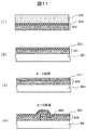
- FIG. 12 is a process diagram for explaining an example of the manufacturing method of the capacitive coupling touch panel shown in FIG. 8 following FIG. 11.
- the display device with a touch panel input device of the present invention is provided with a transparent electrode for detecting XY position coordinates on a transparent substrate, and the position touched with respect to the transparent electrode is statically detected. It has a structure in which a touch panel substrate with a capacitive coupling type touch panel that is detected by capacitive coupling as an input device is bonded to the upper surface of the display device, and has a wavelength on the upper surface side of the touch panel substrate or on the upper surface side and lower surface side of the touch panel. A light transmission layer that transmits visible light of 430 nm or more is provided.
- the transparent electrode is composed of a conductive film containing metal nanowires in a transparent resin, laminated on a part of the surface of the conductive film, and exposed from the surface layer of the transparent resin. And a connection electrode for connecting the lead-out wiring for connecting to the external circuit of the touch panel and the transparent electrode.
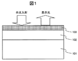
- the display device with a capacitively coupled touch panel input device of the first embodiment is shown in a sectional view of FIG.
- the display device with the capacitive coupling type touch panel input device of the present embodiment includes a capacitive coupling type touch panel 102 on the upper surface of the display device 101, and further transmits light having a wavelength of 430 nm or more on the upper surface of the touch panel.
- a light transmitting layer 103 having a specific wavelength band serving as a layer is provided.
- the display device 101 is a liquid crystal display device
- the liquid crystal display device 201 has the following structure.
- a display circuit which is a pixel assembly of thin film transistor circuits arranged in a matrix on a first transparent substrate 205 is provided, and a second transparent substrate 207 is provided on an opposing surface of the first transparent substrate 205, and the opposing substrate
- a liquid crystal layer 206 sandwiched between 205 and 207 is provided.
- the substrates 205 and 207 are provided two polarizing plates 204 and 208 that are in a combination of optical orthogonal states with respect to the polarized light, and the light emission in the visible light region from the backlight 203 is the polarizing plate 204 and the substrate 205.
- the light passes through the polarizing plate 208 as image display light.
- a capacitively coupled touch panel 202 (details of the configuration of the touch panel will be described later) is bonded to the upper surface of the liquid crystal display device 201 via an optically transparent adhesive layer 209.
- the touch panel 202 includes a touch panel transparent electrode circuit 211 for detecting touch position coordinates on the surface of the touch panel transparent substrate 210.
- a cover transparent substrate 213 that protects the surface is bonded to the upper surface of the touch panel 202 via an optically transparent adhesive layer 212.
- the cover transparent substrate surface is provided with a light transmission layer 214 in a specific wavelength range that serves as a light transmission layer that transmits visible light having a wavelength of 430 nm or more.
- the light transmitting layer 214 is present on the surface of the cover transparent substrate 213, but conversely, the light transmitting layer 214 may be provided in the lower layer and the cover transparent substrate 213 may be provided on the outermost surface.
- the liquid crystal display device 201 drives the liquid crystal as an optical shutter, and the liquid crystal driving method includes FFS (Fringe Field Switching), IPS (In-Place-Switching), VA (Vertical Alignment), and TN. (Twisted Nematic) are known and can be used.
- a glass substrate such as alkali glass such as soda glass or borosilicate glass, non-alkali glass, or chemically strengthened glass is suitable.
- polyester films such as polyethylene terephthalate having transparency and polyethylene naphthalate, polyimide films having high heat resistance and transparency are also known, and it is also possible to use such resin-based substrates having transparency. .
- the light transmission layer 214 that transmits visible light having a wavelength of 430 nm or more used in the present invention is made of a material film in which semiconductor compound fine particles having a band gap at a light wavelength of less than 430 nm are contained in an optically transparent resin. It is suitable for transmitting visible light having a wavelength of 430 nm or more by light absorption and light scattering reflection of semiconductor compound fine particles.
- semiconductor compound fine particles having a band gap at an optical wavelength of less than 430 nm those obtained by adding compound fine particles mainly composed of SiC fine particles and selected from ZnO, WO 3 , TiO 2 and SrTiO 3 are suitable.
- As the shape of the fine particles a diameter range of 10 nm to 100 nm is suitable.
- polyolefin resin As the optically transparent resin containing semiconductor compound fine particles, polyolefin resin, polyester resin, polyamide resin, polyimide resin, polystyrene resin, polycarbonate resin, acrylic resin and the like are suitable. More specifically, polyethylene, polypropylene, cyclic polyolefin, polyethylene terephthalate, polyethylene naphthalate, polybutylene terephthalate, polylactic acid, nylon, polycarbonate, polyester carbonate, polymethyl methacrylate, polyethyl methacrylate, and the like are suitable. In the case of a polyimide resin, a polyimide having a structure combining a diphenyl ether skeleton or a biphenyl skeleton as a molecular structure is desirable.
- the light transmitting layer 214 that transmits visible light having a wavelength of 430 nm or more used in the present invention includes a light absorbing material made of a compound having an absorbance maximum at a light wavelength of 380 nm or more and less than 430 nm, or a light wavelength of 380 nm or more and less than 430 nm A material composed of a molecular structure having an absorbance maximum is included.
- a diameter range of 10 nm to 100 nm is suitable.
- the compound having an absorbance maximum at a light wavelength of 380 nm or more and less than 430 nm copper halide fine particles, silver fine particles and the like are suitable.
- the shape of the fine particles a diameter range of 10 nm to 100 nm is suitable.
- a material comprising a molecular structure having an absorbance maximum at a light wavelength of 380 nm or more and less than 430 nm a polyimide resin having a structure combining a diphenyl ether skeleton or a biphenyl skeleton as the molecular structure is suitable.
- the light transmission layer that transmits visible light having a wavelength of 430 nm or more has a light transmittance of 50% or more of the wavelength of 430 nm or more.
- optically transparent adhesive layer 209 a liquid adhesive material or an adhesive tape generally called an optically transparent adhesive (Optically Clear Adhesive) is suitable.
- optically transparent adhesive Optically Clear Adhesive
- cover transparent substrate 213 chemically strengthened glass is suitable.
- the cover transparent substrate 213 and the specific wavelength region light transmission layer 214 are separately provided.
- the chemically tempered glass to be the cover transparent substrate SiC, ZnO, WO 3 , TiO 2 , SrTiO 3 , halogen
- fine particles such as copper chloride and silver
- a diameter range of 10 nm to 100 nm is suitable.
- the display device with a capacitively coupled touch panel input device of the second embodiment is shown in the cross-sectional view of FIG.
- the capacitive coupling type touch panel 302 is bonded to the upper surface of the liquid crystal display device 301 via an optically transparent adhesive layer 309.
- the touch panel 302 includes a touch panel transparent electrode circuit 310 for detecting touch position coordinates on the surface of the touch panel transparent substrate 311.
- a second specific wavelength region light transmission layer 312 serving as a light transmission layer that transmits visible light having a wavelength of 430 nm or more is provided on the upper surface of the touch panel transparent substrate 311.
- the touch panel transparent substrate 311 and the specific wavelength region light transmission layer 312 are separately provided.
- the transparent substrate SiC, ZnO, WO 3 , TiO 2 , SrTiO 3 , copper halide, silver, etc.
- fine particles or the like it is possible to integrate the function of the specific wavelength region light transmission layer into the transparent substrate.
- a diameter range of 10 nm to 100 nm is suitable.
- a display device with a capacitively coupled touch panel input device is shown in a sectional view of FIG.
- the display device with the capacitive coupling touch panel input device includes a first specific wavelength region light transmission layer 402 serving as a light transmission layer that transmits visible light having a wavelength of 430 nm or more on the upper surface of the display device 401.
- a capacitive coupling type touch panel 403 is provided on the upper surface, and a second specific wavelength region light transmitting layer 404 serving as a light transmitting layer that transmits visible light having a wavelength of 430 nm or more is provided on the upper surface of the touch panel.
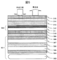
- FIG. 5 is a cross-sectional view of an embodiment in which the display device is a liquid crystal display device.
- the liquid crystal display device 501 has the following structure.
- a display circuit which is a pixel assembly of thin film transistor circuits arranged in a matrix on a first transparent substrate 505 is provided, and a second transparent substrate 507 is provided on the opposite surface of the first transparent substrate 505.
- a liquid crystal layer 506 sandwiched between 505 and 507 is provided.
- the substrates 505 and 507 there are two polarizing plates 504 and 508 that are in a combination of optical orthogonal states with respect to the polarized light, and the light emission from the backlight 503 in the visible light region is the polarizing plate 504 and the substrate 505. Then, the light passes through the polarizing plate 508 as image display light.
- the upper surface of the liquid crystal display device 501 includes a first specific wavelength range light transmission layer 510 serving as a light transmission layer that transmits visible light having a wavelength of 430 nm or more through an optically transparent adhesive layer 509, and the upper surface thereof.
- the touch panel 502 includes a touch panel transparent electrode circuit 512 for detecting touch position coordinates on the surface of the touch panel transparent substrate 511.
- a cover transparent substrate 514 that protects the surface is bonded to the upper surface of the touch panel 502 via an optically transparent adhesive layer 513.
- the cover transparent substrate surface is provided with a second specific wavelength region light transmission layer 515 serving as a light transmission layer that transmits visible light having a wavelength of 430 nm or more.
- the light transmission layer 515 is present on the surface of the cover transparent substrate 514, but conversely, the light transmission layer 515 may be provided in the lower layer and the cover transparent substrate 514 may be provided on the outermost surface.
- the cover transparent substrate 514 and the specific wavelength range light transmission layer 515 are separately provided.
- the chemically strengthened glass to be the cover transparent substrate SiC, ZnO, WO 3 , TiO 2 , SrTiO 3 are used.
- fine particles such as copper halide and silver, it is possible to integrate the function of the light transmitting layer in the specific wavelength region into the cover transparent substrate.
- the shape of the fine particles a diameter range of 10 nm to 100 nm is suitable.
- the touch panel transparent substrate 511 and the specific wavelength band light transmission layer 510 are separately provided.
- the transparent substrate SiC, ZnO, WO 3 , TiO 2 , SrTiO 3 , copper halide, silver It is also possible to integrate the function of the specific wavelength region light transmission layer into the transparent substrate by including fine particles such as. As the shape of the fine particles, a diameter range of 10 nm to 100 nm is suitable.
- the touch panel transparent substrate 511 it is also possible to integrate the function of the light transmission layer in a specific wavelength region into the transparent substrate by using a polyimide resin having a structure in which a diphenyl ether skeleton or a biphenyl skeleton is combined as a molecular structure. .
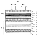
- a display device with a capacitively coupled touch panel input device is shown in a sectional view of FIG.
- a display device with a capacitively coupled touch panel input device has a first specific wavelength band light transmitting layer 609 serving as a light transmitting layer that transmits visible light having a wavelength of 430 nm or more directly on the upper surface of the liquid crystal display device 601.
- a capacitively coupled touch panel 602 is bonded through an optically transparent adhesive layer 610.
- the touch panel 602 includes a touch panel transparent electrode circuit 611 for detecting touch position coordinates on the surface of the touch panel transparent substrate 612.
- a second specific wavelength region light transmission layer 613 is provided on the upper surface of the touch panel transparent substrate 612 as a light transmission layer that transmits visible light having a wavelength of 430 nm or more.
- a display device with a capacitively coupled touch panel input device is shown in a sectional view of FIG.
- the display device with a capacitively coupled touch panel input device of this embodiment includes an organic electroluminescence display device 701.
- a display circuit layer 704 which is a pixel aggregate of thin film transistor circuits arranged in a matrix on a first substrate 703 of a display device 701 is provided, and an ultrathin film of an organic electroluminescent material is formed between electrode layers connected to the thin film transistor circuit on the upper layer.
- a circuit layer 705 in which the organic electroluminescent material emits light by applying current to the electrode is provided.
- a transparent substrate 707 bonded to the opposite surface of the substrate 703 with a transparent sealing layer 706 for light transmission is sealed from the outside environment.
- Light emitted from the organic electroluminescence light emitting circuit layer 705 is transmitted through the sealing layer 706 and the counter substrate 707 to become display light, whereby the organic electroluminescence display device 701 is realized.
- a capacitive coupling type touch panel 702 is bonded to the upper surface of the display device 701 through an optically transparent adhesive layer 708.
- the touch panel 702 includes a touch panel transparent electrode circuit 710 for detecting touch position coordinates on the surface of the touch panel transparent substrate 709.
- a cover transparent substrate 712 that protects the surface is bonded to the upper surface of the touch panel 702 via an optically transparent adhesive layer 711.
- the cover transparent substrate surface is provided with a light transmitting layer 713 having a specific wavelength range that serves as a light transmitting layer that transmits visible light having a wavelength of 430 nm or more.
- the light transmissive layer 713 is present on the surface of the cover transparent substrate 712. Conversely, the light transmissive layer 713 may be provided on the lower layer, and the cover transparent substrate 712 may be provided on the outermost surface.
- the cover transparent substrate 712 and the specific wavelength region light transmission layer 713 are separately provided.
- the chemically tempered glass serving as the cover transparent substrate SiC, ZnO, WO 3 , TiO 2 , SrTiO 3 are used.
- fine particles such as copper halide and silver, it is possible to integrate the function of the light transmitting layer in the specific wavelength region into the cover transparent substrate.
- a diameter range of 10 nm to 100 nm is suitable.
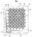
- the capacitive coupling type touch panel according to Examples 1 to 5 described above is shown in the substrate plan view of FIG.
- this touch panel there is a touch screen 802 that is an area for detecting touch position coordinates on one surface of a transparent substrate 801, and each transparent electrode 803 that detects an electrostatic capacitance change and outputs X and Y position coordinates in this area. , 804.
- Transparent electrodes 803 for detecting the X position coordinates are connected to the transparent electrodes 803 corresponding to the same X position coordinates, and the transparent electrodes 804 for detecting the Y position coordinates correspond to the same Y position coordinates.
- the transparent electrodes 804 are connected to each other.
- These transparent electrodes are provided with a lead wiring 805 for connecting to an element circuit for controlling an electrical signal as a touch panel, an electrode 806 for connecting the lead wiring and the transparent electrode, and a terminal portion 807 for connecting to a drive circuit element. Has been.
- glass substrates such as soda glass, alkali glass such as borosilicate glass, non-alkali glass, and chemically strengthened glass are suitable.
- polyester films such as polyethylene terephthalate having transparency and polyethylene naphthalate, polyimide films having high heat resistance and transparency are also known, and it is possible to use such resin-based substrates having transparency. .
- a metal electrode formed by sputtering or vapor deposition is suitable. Specific examples include alloys such as Ag—Pd—Cu, Al—Cu, Ni—Cu, Al, Cu, and Ni, laminated electrodes, and single electrodes. Further, it can be formed using an Ag conductive paste.
- FIG. 9 shows an enlarged view and a cross-sectional structure of the connection portion between the lead wiring 805 and the transparent electrode 804 that outputs the Y position coordinates.
- the electrode 806 that connects the lead wiring 805 and the transparent electrode 804 is formed in a structure that is laminated on the end of the transparent electrode 804 when the lead wiring 805 is formed. It is not required.
- the transparent electrodes 804 are connected to the lead-out wiring 805 by connecting the transparent electrodes corresponding to the same Y position coordinate.
- the cross-sectional structure of the connection portion between the lead wiring 805 and the transparent electrode 803 that outputs the X position coordinate is the same.
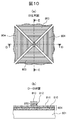
- FIG. 10 shows an enlarged B view and a DD cross-sectional structure at the intersection of the connection portions of the transparent electrodes 803 and 804 corresponding to these X and Y position coordinates.
- the intersection of the connecting portion of the transparent electrode 803 that outputs the X coordinate is insulated from the connecting portion of the transparent electrode 804 that outputs the Y position coordinate by the transparent resin layer 812 made of an insulating resin.
- the metal nanowires contained in the transparent electrodes 803 and 804 nanowires such as Ag, Cu, Co, C, and Pd can be used.
- Ag nanowire is the most suitable constituent material from the viewpoints of conductivity and light transmission as a conductive film.
- the metal nanowires in this touch panel have a cross-sectional diameter of 10 to 100 nm and a length of 1 to 100 ⁇ m. Further, this touch panel has a structure in which a transparent resin 810, 812 of a conductive film is bonded to the surface of the transparent substrate 801, and the surface layer (811, 813) of the conductive film contains metal nanowires in a thickness of 10 to 200 nm. . Further, metal nanowires may be unevenly distributed on the surface side of the transparent substrate 801 (with a thickness of 10 to 200 nm from the surface).
- the touch panel of Example 6 was manufactured under the following conditions in the steps shown in FIGS. First, as shown in FIG. 11 (1), a photosensitive resin composition film 821 in which metal nanowires are contained in a transparent resin (the photosensitive resin composition film described in “WO2010 / 021224” can be used.
- a support film 822 provided with a) is prepared. This is a member having a film structure in which a photosensitive resin composition film 821 is laminated on a support film 822 for supporting the photosensitive resin composition film 821.
- This photosensitive resin composition film 821 includes a metal nanowire-containing layer 823.
- a photosensitive resin composition film 821 including a metal nanowire-containing layer 823 laminated on a support film 822 is bonded to a transparent substrate 801 by film transfer.
- the photosensitive resin composition film 821 is exposed to a desired shape through a light shielding mask, and an unexposed portion in the exposure step is removed using an alkaline developer.
- a transparent electrode 804 that outputs a Y position coordinate formed of a conductive film 811 of metal nanowires contained in a transparent resin 810 formed in a desired shape on a transparent substrate 801 is formed.
- FIG. 11 (3) represents the DD cross section of FIG. 10
- FIG. 11 (4) represents the EE cross section of FIG.
- the desired shape is exposed through a light-shielding mask, and an unexposed portion in the exposure process is exposed using an alkaline developer.
- the transparent electrode 803 that outputs the X position coordinates composed of the conductive film 813 of the metal nanowire contained in the transparent resin 812 formed in a desired shape on the transparent substrate 801 is removed.
- a lead wire 805 for connecting to an external circuit and a connection electrode 806 for connecting the lead wire 805 and the transparent electrode 804 are formed on the surface of the transparent substrate 801.
- the lead wiring 805 and the connection electrode 806 are formed at the same time by screen printing using a conductive paste material containing flaky Ag.
- the relative positional relationship between the metal nanowires is film transfer. Since the conductive film is not changed even after the conductive film is formed by exposure or development, it is possible to create a capacitive coupling type touch panel having transparent electrodes 803 and 804 having high-quality XY position coordinates. A display device with a combined touch panel input device is realized.
- Cover transparent substrate 214 ... Specific wavelength range light transmission layer , DESCRIPTION OF SYMBOLS 301 ... Liquid crystal display device 302 ... Capacitance coupling type touch panel, 303 ... Back light, 304 ... 1st polarizing plate, 305 ... 1st transparent substrate (thin-film transistor circuit board), 306 ... Liquid crystal layer, 307 ... 2nd 308 ... second polarizing plate, 309 ... optical transparency adhesive layer, 310 ... touch panel transparent electrode circuit, 311 ... touch panel transparent substrate, 312 ... specific wavelength band light transmission layer, 401 ... display device 402 ... first specific wavelength range light transmission layer, 403 ... capacitive coupling touch panel, 404 ...
- second specific wavelength range light transmission layer 501 ... Liquid crystal display device, 502 ... Capacitive coupling type touch panel, 503 ... Backlight, 504 ... First polarizing plate, 505 ... First transparent substrate (thin film transistor circuit substrate), 506 ... Liquid crystal layer, 507 ... Second 508 ... second polarizing plate, 509 ... optical transparency adhesive layer, 510 ... first specific wavelength region light transmission layer, 511 ... touch panel transparent substrate, 512 ... touch panel transparent electrode circuit, 513 ... optical Transparent adhesive layer, 514 ... cover transparent substrate, 515 ... second specific wavelength range light transmitting layer, 601 ... Liquid crystal display device, 602 ... Capacitive coupling type touch panel, 603 ...
- First polarizing plate 605 ... First transparent substrate (thin film transistor circuit substrate), 606 ... Liquid crystal layer, 607 ... Second 608 ... second polarizing plate, 609 ... first specific wavelength range light transmission layer, 610 ... optical transparency adhesive layer, 611 ... touch panel transparent electrode circuit, 612 ... touch panel transparent substrate, 613 ... second Specific wavelength region light transmission layer, 701 ... Organic electroluminescence display device, 702 ... Capacitive coupling type touch panel, 703 ... First substrate, 704 ... Thin film transistor circuit substrate layer, 705 ... Organic electroluminescence light emitting circuit layer, 706 ... Optical transparent sealing layer, 707 ... Opposite sealing transparent substrate, 708 ...
Landscapes
- Physics & Mathematics (AREA)
- Engineering & Computer Science (AREA)
- General Physics & Mathematics (AREA)
- Nonlinear Science (AREA)
- Optics & Photonics (AREA)
- Theoretical Computer Science (AREA)
- General Engineering & Computer Science (AREA)
- Mathematical Physics (AREA)
- Crystallography & Structural Chemistry (AREA)
- Chemical & Material Sciences (AREA)
- Human Computer Interaction (AREA)
- Computer Networks & Wireless Communication (AREA)
- Microelectronics & Electronic Packaging (AREA)
- Position Input By Displaying (AREA)
- Liquid Crystal (AREA)
Priority Applications (3)
| Application Number | Priority Date | Filing Date | Title |
|---|---|---|---|
| US15/325,781 US20170168337A1 (en) | 2014-07-15 | 2015-07-02 | Display Device with Capacitive Coupling Type Touch Panel Input Device |
| KR1020177001068A KR20170018922A (ko) | 2014-07-15 | 2015-07-02 | 정전 용량 결합 방식 터치 패널 입력 장치 부착 표시 장치 |
| CN201580038014.5A CN106537306A (zh) | 2014-07-15 | 2015-07-02 | 带静电电容耦合方式触摸屏输入装置的显示装置 |
Applications Claiming Priority (2)
| Application Number | Priority Date | Filing Date | Title |
|---|---|---|---|
| JP2014144900A JP2016021170A (ja) | 2014-07-15 | 2014-07-15 | 静電容量結合方式タッチパネル入力装置付き表示装置 |
| JP2014-144900 | 2014-07-15 |
Publications (1)
| Publication Number | Publication Date |
|---|---|
| WO2016009851A1 true WO2016009851A1 (ja) | 2016-01-21 |
Family
ID=55078349
Family Applications (1)
| Application Number | Title | Priority Date | Filing Date |
|---|---|---|---|
| PCT/JP2015/069166 Ceased WO2016009851A1 (ja) | 2014-07-15 | 2015-07-02 | 静電容量結合方式タッチパネル入力装置付き表示装置 |
Country Status (6)
| Country | Link |
|---|---|
| US (1) | US20170168337A1 (enExample) |
| JP (1) | JP2016021170A (enExample) |
| KR (1) | KR20170018922A (enExample) |
| CN (1) | CN106537306A (enExample) |
| TW (1) | TWI576751B (enExample) |
| WO (1) | WO2016009851A1 (enExample) |
Families Citing this family (8)
| Publication number | Priority date | Publication date | Assignee | Title |
|---|---|---|---|---|
| WO2018066214A1 (ja) * | 2016-10-06 | 2018-04-12 | アルプス電気株式会社 | 静電容量式センサ |
| JP2019036399A (ja) * | 2017-08-10 | 2019-03-07 | 株式会社小糸製作所 | 車両用表示装置 |
| US20210165511A1 (en) | 2018-01-11 | 2021-06-03 | Mitsubishi Paper Mills Limited | Conductive material and treatment method |
| CN110322782B (zh) * | 2018-03-28 | 2021-12-07 | 英属开曼群岛商镎创科技股份有限公司 | 显示基板与显示面板 |
| TWI662521B (zh) * | 2018-03-28 | 2019-06-11 | 英屬開曼群島商錼創科技股份有限公司 | 顯示基板與顯示面板 |
| US11003226B1 (en) * | 2018-08-09 | 2021-05-11 | Rockwell Collins, Inc. | Touchscreen sensor electromagnetic interference protection apparatus |
| CN113900348A (zh) * | 2020-07-06 | 2022-01-07 | 京东方科技集团股份有限公司 | 投影幕布及其制造方法、投影显示系统及显示方法 |
| WO2022025314A1 (ko) * | 2020-07-29 | 2022-02-03 | 주식회사 예건 | 열차용 통합안테나장치 |
Citations (6)
| Publication number | Priority date | Publication date | Assignee | Title |
|---|---|---|---|---|
| JP2003011284A (ja) * | 2001-07-04 | 2003-01-15 | Mitsui Chemicals Inc | 積層フィルムないしシート、およびその製造方法 |
| JP2004255635A (ja) * | 2003-02-25 | 2004-09-16 | Dainippon Printing Co Ltd | 透明積層フィルム、反射防止フィルム及びそれを用いた偏光板、液晶表示装置 |
| JP2007178915A (ja) * | 2005-12-28 | 2007-07-12 | Fujifilm Corp | 金属微粒子分散物及び赤外線遮蔽フィルター |
| JP2012254621A (ja) * | 2011-05-19 | 2012-12-27 | Arakawa Chem Ind Co Ltd | ガスバリア性積層ポリイミドフィルム、機能性薄膜層積層ガスバリア性積層ポリイミドフィルム、ディスプレイ及び太陽電池 |
| JP2013200891A (ja) * | 2011-12-05 | 2013-10-03 | Hitachi Chemical Co Ltd | タッチパネル用電極の保護膜及びタッチパネル |
| JP2014010516A (ja) * | 2012-06-28 | 2014-01-20 | Hitachi Chemical Co Ltd | 静電容量結合方式タッチパネルおよびその製造方法 |
Family Cites Families (15)
| Publication number | Priority date | Publication date | Assignee | Title |
|---|---|---|---|---|
| US5352725A (en) * | 1991-09-27 | 1994-10-04 | Kerr-Mcgee Chemical Corporation | Attenuation of polymer substrate degradation due to ultraviolet radiation |
| JP3740492B2 (ja) * | 2003-01-31 | 2006-02-01 | トライアル株式会社 | 密度を制御した微小粒子 |
| CN101493532A (zh) * | 2008-01-24 | 2009-07-29 | Tcl集团股份有限公司 | 一种显示装置 |
| US20100108409A1 (en) * | 2008-11-06 | 2010-05-06 | Jun Tanaka | Capacitive coupling type touch panel |
| EP3521986B1 (en) * | 2011-01-19 | 2020-05-20 | Lg Innotek Co. Ltd | Touch panel |
| KR101861737B1 (ko) * | 2011-11-17 | 2018-05-29 | 삼성디스플레이 주식회사 | 광학 유닛 및 이를 포함하는 표시 장치 |
| WO2013084284A1 (ja) * | 2011-12-05 | 2013-06-13 | 日立化成株式会社 | タッチパネル用電極の保護膜の形成方法、感光性樹脂組成物及び感光性エレメント |
| KR20170106655A (ko) * | 2011-12-05 | 2017-09-21 | 히타치가세이가부시끼가이샤 | 터치패널용 전극의 보호막의 형성 방법, 감광성 수지 조성물 및 감광성 엘리먼트, 및, 터치패널의 제조 방법 |
| WO2013084282A1 (ja) * | 2011-12-05 | 2013-06-13 | 日立化成株式会社 | 樹脂硬化膜パターンの形成方法、感光性樹脂組成物及び感光性エレメント |
| DE112013007837B3 (de) * | 2012-07-20 | 2023-08-17 | Semiconductor Energy Laboratory Co., Ltd. | Anzeigevorrichtung |
| JP6144548B2 (ja) * | 2012-08-01 | 2017-06-07 | 日東電工株式会社 | 透明導電性積層フィルム、その製造方法及びタッチパネル |
| US9354755B2 (en) * | 2012-11-27 | 2016-05-31 | Guardian Industries Corp. | Projected capacitive touch panel with a silver-inclusive transparent conducting layer(s) |
| JP5987668B2 (ja) * | 2012-12-06 | 2016-09-07 | 日立化成株式会社 | 表示装置およびその製造方法 |
| TWM465615U (zh) * | 2013-05-31 | 2013-11-11 | Hitachi Chemical Co Ltd | 觸碰面板 |
| CN103646958A (zh) * | 2013-11-18 | 2014-03-19 | 上海和辉光电有限公司 | 一种显示面板及其制作方法 |
-
2014
- 2014-07-15 JP JP2014144900A patent/JP2016021170A/ja active Pending
-
2015
- 2015-06-09 TW TW104118653A patent/TWI576751B/zh not_active IP Right Cessation
- 2015-07-02 CN CN201580038014.5A patent/CN106537306A/zh not_active Withdrawn
- 2015-07-02 WO PCT/JP2015/069166 patent/WO2016009851A1/ja not_active Ceased
- 2015-07-02 KR KR1020177001068A patent/KR20170018922A/ko not_active Ceased
- 2015-07-02 US US15/325,781 patent/US20170168337A1/en not_active Abandoned
Patent Citations (6)
| Publication number | Priority date | Publication date | Assignee | Title |
|---|---|---|---|---|
| JP2003011284A (ja) * | 2001-07-04 | 2003-01-15 | Mitsui Chemicals Inc | 積層フィルムないしシート、およびその製造方法 |
| JP2004255635A (ja) * | 2003-02-25 | 2004-09-16 | Dainippon Printing Co Ltd | 透明積層フィルム、反射防止フィルム及びそれを用いた偏光板、液晶表示装置 |
| JP2007178915A (ja) * | 2005-12-28 | 2007-07-12 | Fujifilm Corp | 金属微粒子分散物及び赤外線遮蔽フィルター |
| JP2012254621A (ja) * | 2011-05-19 | 2012-12-27 | Arakawa Chem Ind Co Ltd | ガスバリア性積層ポリイミドフィルム、機能性薄膜層積層ガスバリア性積層ポリイミドフィルム、ディスプレイ及び太陽電池 |
| JP2013200891A (ja) * | 2011-12-05 | 2013-10-03 | Hitachi Chemical Co Ltd | タッチパネル用電極の保護膜及びタッチパネル |
| JP2014010516A (ja) * | 2012-06-28 | 2014-01-20 | Hitachi Chemical Co Ltd | 静電容量結合方式タッチパネルおよびその製造方法 |
Also Published As
| Publication number | Publication date |
|---|---|
| TW201602887A (zh) | 2016-01-16 |
| CN106537306A (zh) | 2017-03-22 |
| JP2016021170A (ja) | 2016-02-04 |
| TWI576751B (zh) | 2017-04-01 |
| KR20170018922A (ko) | 2017-02-20 |
| US20170168337A1 (en) | 2017-06-15 |
Similar Documents
| Publication | Publication Date | Title |
|---|---|---|
| WO2016009851A1 (ja) | 静電容量結合方式タッチパネル入力装置付き表示装置 | |
| TWI477851B (zh) | 觸控顯示面板與觸控液晶顯示面板 | |
| US8816982B2 (en) | Method of manufacturing transparent circuit substrate for touch screen | |
| TWI536217B (zh) | 觸控顯示裝置 | |
| US10289224B2 (en) | Pressure sensing display and manufacturing method thereof | |
| CN101539676B (zh) | 触控式显示装置、触控式液晶显示装置及其制造方法 | |
| US20110254778A1 (en) | Slim type touch device | |
| CN106249979A (zh) | 触控电极结构以及触控显示装置 | |
| CN103543486A (zh) | 具有透明电屏蔽层的触摸屏显示器 | |
| CN203386163U (zh) | 触控显示装置 | |
| JP2011070092A (ja) | 液晶表示装置 | |
| TW202009673A (zh) | 觸控顯示裝置 | |
| CN101937145A (zh) | 显示装置 | |
| JP2015011121A (ja) | 液晶表示装置 | |
| CN101840290A (zh) | 反射式触控显示面板及其制造方法 | |
| JP2016021170A5 (enExample) | ||
| JP5923417B2 (ja) | 表示装置及びカバー部材 | |
| CN103529975A (zh) | 触控式立体影像控制模块及触控式立体显示装置 | |
| JP5987668B2 (ja) | 表示装置およびその製造方法 | |
| CN102236446B (zh) | 薄型化触控装置 | |
| CN104297973B (zh) | 触摸显示屏 | |
| CN103092377B (zh) | 触控面板及应用其触控面板的触控显示器 | |
| TWI718470B (zh) | 觸控偏光結構及其應用之觸控顯示裝置 | |
| KR102193795B1 (ko) | 보강부재가 도포된 터치 패널 | |
| CN107045397B (zh) | 压力传感装置及其制造方法 |
Legal Events
| Date | Code | Title | Description |
|---|---|---|---|
| 121 | Ep: the epo has been informed by wipo that ep was designated in this application |
Ref document number: 15822870 Country of ref document: EP Kind code of ref document: A1 |
|
| WWE | Wipo information: entry into national phase |
Ref document number: 15325781 Country of ref document: US |
|
| ENP | Entry into the national phase |
Ref document number: 20177001068 Country of ref document: KR Kind code of ref document: A |
|
| NENP | Non-entry into the national phase |
Ref country code: DE |
|
| 122 | Ep: pct application non-entry in european phase |
Ref document number: 15822870 Country of ref document: EP Kind code of ref document: A1 |