WO2016002683A1 - 半導体発光素子及びその製造方法 - Google Patents
半導体発光素子及びその製造方法 Download PDFInfo
- Publication number
- WO2016002683A1 WO2016002683A1 PCT/JP2015/068607 JP2015068607W WO2016002683A1 WO 2016002683 A1 WO2016002683 A1 WO 2016002683A1 JP 2015068607 W JP2015068607 W JP 2015068607W WO 2016002683 A1 WO2016002683 A1 WO 2016002683A1
- Authority
- WO
- WIPO (PCT)
- Prior art keywords
- semiconductor layer
- layer
- type
- semiconductor
- light emitting
- Prior art date
- Legal status (The legal status is an assumption and is not a legal conclusion. Google has not performed a legal analysis and makes no representation as to the accuracy of the status listed.)
- Ceased
Links
Images











Classifications
-
- H—ELECTRICITY
- H10—SEMICONDUCTOR DEVICES; ELECTRIC SOLID-STATE DEVICES NOT OTHERWISE PROVIDED FOR
- H10H—INORGANIC LIGHT-EMITTING SEMICONDUCTOR DEVICES HAVING POTENTIAL BARRIERS
- H10H20/00—Individual inorganic light-emitting semiconductor devices having potential barriers, e.g. light-emitting diodes [LED]
- H10H20/80—Constructional details
- H10H20/81—Bodies
- H10H20/822—Materials of the light-emitting regions
- H10H20/824—Materials of the light-emitting regions comprising only Group III-V materials, e.g. GaP
- H10H20/825—Materials of the light-emitting regions comprising only Group III-V materials, e.g. GaP containing nitrogen, e.g. GaN
Definitions
- the present invention relates to a semiconductor light emitting device and a method of manufacturing the same.
- FIG. 6 is a cross-sectional view schematically showing the structure of the semiconductor light emitting device disclosed in the same document.
- the conventional semiconductor light emitting device 100 shown in FIG. 6 includes a substrate 101, a buffer layer 102, an n-type contact layer 103, an n-type cladding layer 104, an active layer 105, a p-type cladding layer 106, a first p-type contact layer 107, A second p-type contact layer 108 is provided.
- the semiconductor light emitting device 100 further includes an n-side electrode 109 on the top surface of the n-type contact layer 103 and a p-side electrode 110 on the top surface of the second p-type contact layer 108.
- the second p-type contact layer 108 in contact with the p-side electrode 110 is formed of a semiconductor layer having a high p-type impurity concentration and a low Al composition ratio, and the first p-type contact layer 107
- the semiconductor layer is composed of a semiconductor layer having a low p-type impurity concentration and a high Al composition ratio as compared with the second p-type contact layer 108.
- an ohmic contact with the p-side electrode 110 is realized by forming the p-type contact layer (107, 108) with two types of layers having different p-type impurity concentration and Al composition ratio as described above.
- the thickness of the contact layer can be secured to the extent that the device characteristics can be maintained while preventing self-absorption.
- Patent Document 1 the conventional semiconductor light emitting device 100 shown in FIG. 6 is manufactured by the following procedure.
- the buffer layer 102 of GaN is grown at 510 ° C. on the upper layer of the substrate 101
- the n-type contact layer 103 of n-type Al 0.04 Ga 0.96 N is grown at 1050 ° C.
- an n-type cladding layer 104 of n-type Al 0.18 Ga 0.82 N is grown at 1050 ° C. on the n-type contact layer 103, and then an active layer 105 of undoped InGaN is grown at 700 ° C.
- the description of InGaN means In a1 Ga 1 -a1 N (0 ⁇ a1 ⁇ 1) and does not indicate that the composition ratio of In and Ga is 1: 1. .
- the description of AlGaN etc. is also the same.
- a p-type cladding layer 106 of Al 0.2 Ga 0.8 N is grown.
- a first p-type contact layer 107 made of Al 0.04 Ga 0.96 N doped with Mg 1 ⁇ 10 19 / cm 3 is grown on the p-type cladding layer 106 to a thickness of 0.1 ⁇ m.
- the second p-type contact layer 108 made of Al 0.01 Ga 0.99 N doped with 2 ⁇ 10 21 / cm 3 of Mg is grown with a film thickness of 0.02 ⁇ m by adjusting the flow rate of gas. .
- the wafer is annealed at 700 ° C. in the reaction vessel to reduce the resistance of the p-type semiconductor layer, and then the wafer is removed from the reaction vessel.
- a mask having a predetermined shape is formed on the surface of the second p-type contact layer 108 located in the uppermost layer, and the semiconductor layer is etched from the second p-type contact layer 108 side by an RIE (reactive ion etching) device.
- the surface of the n-type contact layer 103 is exposed.
- the n-side electrode 109 is formed on the exposed upper surface of the n-type contact layer 103
- the p-side electrode 110 is formed on the upper surface of the second p-type contact layer 108.
- the p-type cladding layer 106, the first p-type contact layer 107, and the second p-type contact layer 108 are all epitaxially grown with the inside of the furnace at a high temperature of 1000 ° C. or higher. It is formed. Thereafter, the temperature in the furnace is reduced. In the above method, the wafer is cooled to about 700 ° C. and annealed, and then the wafer is taken out of the furnace.
- the semiconductor light emitting device manufactured by the method described above has a high operating voltage.
- An object of the present invention is to realize a semiconductor light emitting device capable of obtaining a high light output while lowering the operating voltage as compared with the related art, and a method of manufacturing the same.
- the inventors of the present invention consider the reason why the operating voltage of the semiconductor light emitting device described in Patent Document 1 is increased by intensive research as follows.
- AlGaN is a mixed crystal of GaN and AlN, and the formation temperature of AlN is higher than the formation temperature of GaN. That is, after the second p-type contact layer 108 made of AlGaN is grown while supplying source gases such as TMG (trimethylgallium), TMA (trimethylaluminum), and ammonia at a high temperature of 1050 ° C., the gas is supplied. Even when stopped, the inside of the furnace is exposed to extremely high temperatures for a while. At this time, GaN among the AlGaN constituting the second p-type contact layer 108 is selectively evaporated, and the Al composition ratio of AlGaN is increased.
- source gases such as TMG (trimethylgallium), TMA (trimethylaluminum), and ammonia
- the band gap of the layer is expanded, and the carrier concentration is lowered.
- the Al-rich layer may be oxidized to form a high resistance layer such as Al 2 O 3 on the surface. For these reasons, the contact resistance between the p-side electrode 110 and the second p-type contact layer 108 is increased, and the operating voltage of the semiconductor light emitting device 100 is increased.
- a method of manufacturing a semiconductor light emitting device is Preparing the substrate (a), On the substrate, n-Al x1 Ga y1 In 1-x1-y1 N (0 ⁇ x1 ⁇ 1,0 ⁇ y1 ⁇ 1) from become n-type forming a first semiconductor layer of (b), Forming an active layer on the first semiconductor layer (c); An upper layer of the active layer, p-Al x2 Ga y2 In 1-x2-y2 N p -type second semiconductor made of (0 ⁇ x2 ⁇ 1,0 ⁇ y2 ⁇ 1) the temperature in the furnace as 800 ° C.
- p-Al x 2 Ga y 2 In 1-x 2-y 2 N (0 ⁇ x 2 ⁇ 1, 1) in the state immediately before the temperature in the furnace decreases, ie, the state immediately before step (f).
- a p-type third semiconductor layer of p-GaN is formed on the top surface of the p-type second semiconductor layer of 0 ⁇ y2 ⁇ 1). That is, even if the supply of gas is stopped when the temperature in the furnace is high, the second semiconductor layer composed of the mixed crystal containing Al is not located on the top surface, so Does not evaporate and the upper surface of the second semiconductor layer becomes Al-rich.
- the third semiconductor layer located on the uppermost surface when the gas supply is stopped is made of p-GaN, it is possible to reduce the temperature from the third semiconductor layer to the GaN during the process of lowering the temperature in the furnace. Even if the H 2 vaporizes, an Al-rich layer is not formed on the top surface of the third semiconductor layer.
- the Al-rich layer is not formed on the upper surface of the p-type semiconductor layer in contact with the p-side electrode, so after the step (f) of reducing the temperature in the furnace Even if the p-side electrode is formed, the contact resistance between the p-side electrode and the third semiconductor layer does not increase. Therefore, a semiconductor light emitting device having a lower operating voltage than conventional is realized. The results are described below with reference to the examples in the section "Forms for carrying out the invention".
- the third semiconductor layer may be a layer having a high doped p-type impurity concentration (eg, 1 ⁇ 10 19 / cm 3 or more).
- the second semiconductor layer may also be a layer having a high doped p-type impurity concentration (for example, 1 ⁇ 10 19 / cm 3 or more).
- all of the third semiconductor layer may be evaporated in the process of step (f).
- the third semiconductor layer functions only as a protective layer for preventing the evaporation of GaN from the mixed crystal containing Al constituting the second semiconductor layer.
- the p-side electrode is formed on the upper surface of the second semiconductor layer.
- the semiconductor layer in contact with the p-side electrode is a second semiconductor layer made of p-Al x2 Ga y2 In 1 -x2-y2 N.
- the second semiconductor layer is an AlGaN layer
- a p-side electrode is formed on the p-AlGaN layer in the same manner as the conventional structure described above with reference to FIG.
- the third semiconductor layer as a protective layer is formed on the upper surface of the second semiconductor layer, particularly in the early stage when the temperature in the furnace is high.
- an Al-rich layer is not formed on the top surface of the second semiconductor layer made of p-Al x 2 Ga y 2 In 1-x 2-y 2 N.
- step (d) p-Al x 2 Ga y 2 In 1-x 2-y 2 N (0 ⁇ x2 ⁇ 1, 0 ⁇ y2 ⁇ 1) may be formed at a temperature at which it can be grown. Absent. Similarly, step (e) may be formed at a temperature higher than that at which p-GaN can be grown.
- the method of manufacturing a semiconductor light emitting device according to the present invention may further include the step (g) of forming an electrode on the upper layer of the third semiconductor layer after the step (f).
- the step (e) may be a step performed by changing only the flow rate of the source gas supplied into the furnace, as compared to the step (d). That is, the growth temperatures may be substantially the same in the step (d) and the step (e).
- the step (e) is a step of growing the semiconductor layer with a high temperature in the furnace following the step (d)
- GaN is not evaporated from the upper surface of the second semiconductor layer consisting of N (0 ⁇ x2 ⁇ 1, 0 ⁇ y2 ⁇ 1) to form an Al-rich layer on the upper surface.
- a third semiconductor layer is formed.
- the thickness of the third semiconductor layer may be 5 nm or less.
- the semiconductor light emitting element when the semiconductor light emitting element is realized as an element which emits ultraviolet light having a peak wavelength of 400 nm or less, it is preferable to make the semiconductor layer made of GaN whose absorption end is located on the longer wavelength side than AlN as thin as possible.
- the third semiconductor layer is provided for the purpose of functioning as a protective layer for preventing formation of an Al-rich layer on the upper surface of the second semiconductor layer, after the execution of step (e) The upper surface of the second semiconductor layer may be covered while the temperature in the furnace is still high.
- the step (e) after the step (e) is performed, at the initial stage of starting the step (f), the temperature in the furnace is high in a state where the gas supply is stopped, so that the third semiconductor layer made of p-GaN Part evaporates. Therefore, the film thickness of the third semiconductor layer after the execution of the step (f) is thinner than the film thickness formed in the step (e).
- the step (e) by setting the growth thickness of the third semiconductor layer such that the thickness of the third semiconductor layer made of p-GaN becomes 5 nm or less after the execution of the step (f), the light output Can be realized.
- the upper layer of the active layer p-Al x3 Ga y3 In 1-x3-y3 N (0 as 800 ° C. or higher temperature in the furnace ⁇ x3 ⁇ 1,0 ⁇ y3 ⁇ 1) having a step (h) of forming a p-type fourth semiconductor layer comprising
- the step (d) may be performed after the step (h) to form the second semiconductor layer having a higher p-type impurity concentration than the fourth semiconductor layer.
- the fourth semiconductor layer can constitute a p-type cladding layer
- the second semiconductor layer can constitute a p-type contact layer.
- a 3rd semiconductor layer remains after execution of a process (f)
- a 2nd semiconductor layer and a 3rd semiconductor layer shall comprise a p-type contact layer.
- the present invention has an n-type semiconductor layer, a p-type semiconductor layer, and an active layer sandwiched between the n-type semiconductor layer and the p-type semiconductor layer on a substrate, and has a peak wavelength of 400 nm or less A semiconductor light emitting device that emits ultraviolet light, and
- the p-type semiconductor layer p-Al x2 Ga y2 In 1-x2-y2 N (0 ⁇ x2 ⁇ 1,0 ⁇ y2 ⁇ 1) and the second semiconductor layer p-type consisting of a film thickness 5nm following p And p-type third semiconductor layer made of GaN;
- the third semiconductor layer is a top layer of the surface of the p-type semiconductor layer opposite to the active layer.
- the third semiconductor layer is composed of p-GaN, but has a film thickness of 5 nm or less, and therefore light absorbed in the third semiconductor layer even when realized as an ultraviolet light emitting element having a peak wavelength of 400 nm or less The amount of can be extremely reduced.
- the semiconductor light emitting device includes the third semiconductor layer made of p-GaN in a layer located on the uppermost surface of the p-type semiconductor layer. More specifically, it means that the layer formed at the position in contact with the p-side electrode can be a third semiconductor layer made of p-GaN.
- the p-type contact layer is formed of a semiconductor layer containing Al such as AlGaN or AlInGaN
- the semiconductor layers are formed in the furnace.
- the GaN is evaporated during the process of decreasing the temperature in the furnace, and an Al-rich layer is formed on the upper surface thereof. As a result, the contact resistance between the layer and the p-side electrode is increased.
- the uppermost surface of the p-type semiconductor layer is the third semiconductor layer formed of p-GaN, the layer rich in Al is not formed on the upper surface of the layer, and the contact resistance with the p-side electrode Resistance can be reduced. Thereby, the operating voltage can be reduced compared to the conventional semiconductor light emitting device.
- the semiconductor light emitting device of the present invention may have an electrode in the upper layer of the third semiconductor layer. More specifically, an electrode may be provided on the surface of the third semiconductor layer opposite to the active layer.
- the p-type semiconductor layer a p-Al x3 Ga y3 In 1 -x3-y3 N (0 ⁇ x3 ⁇ 1,0 ⁇ y3 ⁇ 1) p -type fourth semiconductor layer made of, said fourth semiconductor It is also possible to have the second semiconductor layer formed in the upper layer of the layer and the third semiconductor layer formed in the upper layer of the second semiconductor layer.
- the second semiconductor layer and the third semiconductor layer may have a higher p-type impurity concentration than the fourth semiconductor layer.
- the fourth semiconductor layer can constitute a p-type cladding layer
- the second semiconductor layer can constitute a p-type contact layer.
- n-type semiconductor layer n-Al x1 Ga y1 In 1-x1-y1 N (0 ⁇ x1 ⁇ 1,0 ⁇ y1 ⁇ 1) which is composed of a first semiconductor layer of n-type composed of It does not matter.
- the present invention it is possible to realize a semiconductor light emitting device capable of obtaining a high light output while reducing the operating voltage as compared with the related art.
- FIG. 1 is a cross-sectional view schematically showing a configuration of an embodiment of a semiconductor light emitting device of the present invention. It is sectional drawing which shows typically a part of manufacturing process of the semiconductor light-emitting device of this invention. It is sectional drawing which shows typically a part of manufacturing process of the semiconductor light-emitting device of this invention. It is sectional drawing which shows typically a part of manufacturing process of the semiconductor light-emitting device of this invention. It is sectional drawing which shows typically a part of manufacturing process of the semiconductor light-emitting device of this invention. It is sectional drawing which shows typically a part of manufacturing process of the semiconductor light-emitting device of this invention. It is sectional drawing which shows typically a part of manufacturing process of the semiconductor light-emitting device of this invention.
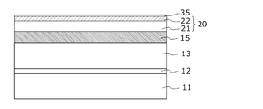
- FIG. 5 is a cross-sectional view schematically showing a structure of a light emitting element of Comparative Example 1
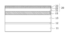
- FIG. 7 is a cross-sectional view schematically showing a structure of a light emitting device of Comparative Example 2.
- FIG. 7 is a cross-sectional view schematically showing a structure of a light emitting device of Comparative Example 3.
- the structure of the semiconductor light emitting device of the present invention will be described below, and then a method of manufacturing the same will be described. Thereafter, performances of the semiconductor light emitting device of the present invention and the conventional semiconductor light emitting device are compared with reference to examples.
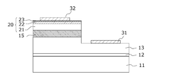
- FIG. 1 is a cross-sectional view schematically showing the configuration of an embodiment of a semiconductor light emitting device of the present invention.
- the semiconductor light emitting device 1 has an n-type semiconductor layer 13, a p-type semiconductor layer 20, and an active layer 15 sandwiched between the n-type semiconductor layer 13 and the p-type semiconductor layer 20 on a growth substrate 11. A more detailed configuration of the semiconductor light emitting device 1 will be described below.
- a semiconductor light emitting device 1 shown in FIG. 1 has an undoped layer 12 on a growth substrate 11, and an n-type semiconductor layer 13 on the undoped layer.
- the semiconductor light emitting device 1 has the active layer 15 on the upper layer of the n-type semiconductor layer 13 and the p-type semiconductor layer 20 on the upper layer of the active layer 15.
- the p-type semiconductor layer 20 is configured to include the p-type semiconductor layer 21, the p-type semiconductor layer 22, and the p-type semiconductor layer 23.
- the n-type semiconductor layer 13 corresponds to the “first semiconductor layer”
- the p-type semiconductor layer 21 corresponds to the “fourth semiconductor layer”
- the p-type semiconductor layer 22 corresponds to the “second semiconductor layer”.
- the p-type semiconductor layer 23 corresponds to the "third semiconductor layer”.
- the n-type semiconductor layer 13 is referred to as a "first semiconductor layer 13”
- the p-type semiconductor layer 21 is referred to as a "fourth semiconductor layer 21”
- the p-type semiconductor layer 22 is referred to as a "second semiconductor layer 22”.
- the p-type semiconductor layer 23 is referred to as "third semiconductor layer 23".
- the third semiconductor layer 23 constitutes the uppermost layer of the surface of the p-type semiconductor layer 20 opposite to the active layer 15.
- the growth substrate 11 is made of, for example, a sapphire substrate.
- the growth substrate 11 may be made of Si, SiC, AlN, AlGaN, GaN, YAG or the like other than sapphire.
- the undoped layer 12 is formed of GaN. More specifically, it is formed of a low temperature buffer layer of GaN and an underlayer of GaN on the low temperature buffer layer.
- the undoped layer 12 is provided on the upper layer of the growth substrate 11 made of, for example, sapphire in order to epitaxially grow the first semiconductor layer 13 and the like in a good state.
- the first semiconductor layer 13 is constituted by n-Al x1 Ga y1 In 1 -x1-y1 N (0 ⁇ x1 ⁇ 1,0 ⁇ y1 ⁇ 1).
- the first semiconductor layer 13 is preferably doped with n-type impurities such as Si, Ge, S, Se, Sn, and Te, and in particular, is preferably doped with Si.
- the first semiconductor layer 13 is formed of n-Al 0.06 Ga 0.94 N.
- the active layer 15 is configured, for example, by periodically repeating a light emitting layer made of InGaN and a barrier layer made of AlGaN. These layers may be undoped or p-type or n-type doped.
- the active layer 15 is not limited to the above materials, and includes a first nitride semiconductor layer and a second nitride semiconductor layer having a larger band gap than the first nitride semiconductor layer, and It suffices to have a configuration in which one nitride semiconductor layer is sandwiched between two second nitride semiconductor layers.
- the first nitride semiconductor layer constitutes a light emitting layer
- the second nitride semiconductor layer constitutes a barrier layer.
- Each material which comprises the active layer 15 is suitably selected according to the peak wavelength of the light to take out.
- the fourth semiconductor layer 21 is composed of p-Al x 3 Ga y 3 In 1-x 3-y 3 N (0 ⁇ x 3 ⁇ 1, 0 ⁇ y 3 ⁇ 1).
- the fourth semiconductor layer 21 is preferably doped with a p-type impurity such as Mg, Be, Zn or C, particularly preferably Mg.
- the fourth semiconductor layer 21 is formed to have a laminated structure of p-Al 0.3 Ga 0.7 N and p-Al 0.13 Ga 0.87 N.
- the second semiconductor layer 22 is composed of p-Al x 2 Ga y 2 In 1-x 2-y 2 N (0 ⁇ x 2 ⁇ 1, 0 ⁇ y 2 ⁇ 1).
- the second semiconductor layer 22 is preferably doped with a p-type impurity such as Mg, Be, Zn or C, particularly preferably Mg.
- the second semiconductor layer 22 is formed of p-Al 0.13 Ga 0.87 N.
- the p-type impurity concentration of the second semiconductor layer 22 is higher than the p-type impurity concentration of the fourth semiconductor layer 21.
- the third semiconductor layer 23 is made of p-GaN having a thickness of 5 nm or less.
- the third semiconductor layer 23 is preferably doped with a p-type impurity such as Mg, Be, Zn or C, in particular, Mg.
- the p-type impurity concentration of the third semiconductor layer 23 is higher than the p-type impurity concentration of the fourth semiconductor layer 21.
- the p-type impurity concentration of the fourth semiconductor layer 21 is about 3 ⁇ 10 19 / cm 3
- the p-type impurity concentration of the second semiconductor layer 22 and the third semiconductor layer 23 is about 1 ⁇ 10 20 / cm 3 It is.
- the third semiconductor layer 23 is formed by passing through the cooling step according to step S8. A part of the film evaporates and the film thickness becomes thin.
- the upper layer of the third semiconductor layer 23 is indicated by a broken line in FIG. 1 in order to indicate that the film thickness decreases after the third semiconductor layer 23 is formed. That is, FIG. 1 shows that the third semiconductor layer 23 corresponding to the broken line portion is evaporated in the process of step S8.
- the semiconductor light emitting device 1 may not necessarily include the fourth semiconductor layer 21. That is, the semiconductor light emitting device 1 may have a configuration in which the second semiconductor layer 22 is provided on the upper surface of the active layer 15.
- the p-type impurity concentration of the second semiconductor layer 22 does not necessarily have to be higher than the p-type impurity concentration of the fourth semiconductor layer 21.
- Step S1 The growth substrate 11 is prepared. More specifically, a c-plane sapphire substrate is prepared as the growth substrate 11, and the substrate is cleaned. More specifically, for this cleaning, for example, the growth substrate 11 (c-plane sapphire substrate) is placed in the processing furnace of a MOCVD (Metal Organic Chemical Vapor Deposition) apparatus, and the flow rate in the processing furnace The temperature is raised to, for example, 1150.degree. C. while flowing hydrogen gas of 10 slm.
- MOCVD Metal Organic Chemical Vapor Deposition
- This step S1 corresponds to the step (a).
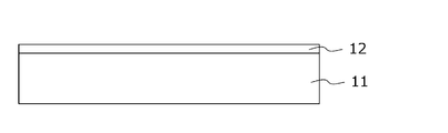
- Step S2 A low temperature buffer layer made of GaN is formed on the surface of the growth substrate 11, and a base layer made of GaN is further formed thereon. These low temperature buffer layers and underlayers correspond to the undoped layer 12.
- a specific method of forming the undoped layer 12 is, for example, as follows. First, the pressure in the furnace of the ⁇ CVD apparatus is 100 kPa, and the temperature in the furnace is 480 ° C. Then, while flowing nitrogen gas and hydrogen gas each having a flow rate of 5 slm as a carrier gas in the processing furnace, TMG having a flow rate of 50 ⁇ mol / min and ammonia having a flow rate of 250,000 ⁇ mol / min are supplied as a source gas into the processing furnace for 68 seconds. Do. Thereby, a low temperature buffer layer of 20 nm in thickness is formed on the surface of the growth substrate 11.
- the temperature in the furnace of the MOCVD apparatus is raised to 1150 ° C. Then, while flowing nitrogen gas having a flow rate of 20 slm and hydrogen gas having a flow rate of 15 slm as a carrier gas in the processing furnace, TMG having a flow rate of 100 ⁇ mol / min and ammonia having a flow rate of 250000 ⁇ mol / min as a source gas in the processing furnace Feed for 30 minutes. Thereby, an underlayer of 1.7 ⁇ m in thickness made of GaN is formed on the surface of the low temperature buffer layer.
- the undoped layer 12 is formed on the growth substrate 11.
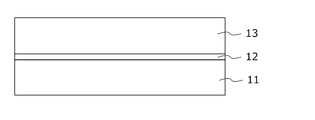
- Step S3 Next, as shown in FIG. 2B, the n-type first semiconductor layer 13 is formed on the undoped layer 12.
- the specific formation method of the first semiconductor layer 13 is, for example, as follows.
- the pressure in the furnace of the MOCVD apparatus is set to 30 kPa. Then, while flowing nitrogen gas having a flow rate of 20 slm and hydrogen gas having a flow rate of 15 slm as carrier gas, TMG having a flow rate of 94 ⁇ mol / min, TMA having a flow rate of 6 ⁇ mol / min, and a flow rate of 250,000 ⁇ mol / min as a carrier gas. Ammonia of min and tetraethylsilane with a flow rate of 0.013 ⁇ mol / min are fed into the processing furnace for 60 minutes.
- the first semiconductor layer 13 having a composition of, for example, n-Al 0.06 Ga 0.94 N, a Si concentration of 5 ⁇ 10 19 / cm 3 and a thickness of 2 ⁇ m is formed in the upper layer of the undoped layer 12 Be done.
- the n-type impurity doped to the first semiconductor layer 13 is Si
- Ge, S, Se, Sn, Te, or the like can be used as the n-type impurity in addition to Si.
- n-GaN having a thickness of about 5 nm may be formed on the upper layer of the first semiconductor layer 13.
- This step S3 corresponds to the step (b).
- Step S4 Next, as shown in FIG. 2C, an active layer in which a light emitting layer composed of, for example, InGaN and a barrier layer composed of n-AlGaN are periodically repeated in the upper layer of the n-type first semiconductor layer 13.
- a light emitting layer composed of, for example, InGaN and a barrier layer composed of n-AlGaN are periodically repeated in the upper layer of the n-type first semiconductor layer 13.
- the pressure in the furnace of the MOCVD apparatus is 100 kPa, and the temperature in the furnace is 830.degree. Then, while flowing nitrogen gas having a flow rate of 15 slm and hydrogen gas having a flow rate of 1 slm as a carrier gas into the processing furnace, TMG having a flow rate of 10 ⁇ mol / min and trimethylindium (TMI) having a flow rate of 12 ⁇ mol / min as a source gas The step of supplying ammonia with a flow rate of 300,000 ⁇ mol / min into the processing furnace for 48 seconds is performed.
- the active layer 15 in which the light emitting layer made of InGaN having a thickness of 2 nm and the barrier layer made of n-AlGaN having a thickness of 7 nm are repeated 15 cycles is a first semiconductor layer 13 Formed in the upper layer of
- This step S4 corresponds to the step (c).
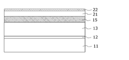
- Step S5 Next, as shown in FIG. 2D, the p-type fourth semiconductor layer 21 is formed on the active layer 15.
- the specific formation method of the fourth semiconductor layer 21 is, for example, as follows.
- the pressure in the furnace of the MOCVD apparatus is maintained at 100 kPa, and the temperature in the furnace is raised to 1025 ° C. while nitrogen gas having a flow rate of 15 slm and hydrogen gas having a flow rate of 25 slm flow as a carrier gas in the processing furnace. Thereafter, TMG having a flow rate of 35 ⁇ mol / min, TMA having a flow rate of 20 ⁇ mol / min, ammonia having a flow rate of 250000 ⁇ mol / min, and biscyclopentadidiene having a flow rate of 0.1 ⁇ mol / min for doping p-type impurities as source gases.
- Enyl magnesium (Cp 2 Mg) is fed into the processing furnace for 60 seconds.
- a hole supply layer having a composition of Al 0.3 Ga 0.7 N having a thickness of 20 nm is formed on the surface of the active layer 15. Thereafter, the flow rate of TMA is changed to 4 ⁇ mol / min and the source gas is supplied for 360 seconds to form a hole supply layer having a composition of Al 0.13 Ga 0.87 N with a thickness of 120 nm.
- the fourth semiconductor layer 21 is formed by these hole supply layers.
- the p-type impurity concentration of the fourth semiconductor layer 21 is, for example, about 3 ⁇ 10 19 / cm 3 .
- the fourth semiconductor layer 21 is formed with the temperature in the furnace set to 1025 ° C., but if the temperature is equal to or higher than the lower limit temperature (eg 800 ° C. or more) at which AlGaN can be grown while doping p-type impurities It is not limited. However, the growth temperature is preferably 900 ° C. or higher, and more preferably 1000 ° C. or higher.
- the lower limit temperature eg 800 ° C. or more
- the growth temperature is preferably 900 ° C. or higher, and more preferably 1000 ° C. or higher.
- This step S5 corresponds to the step (h).
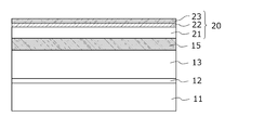
- Step S6 Next, as shown in FIG. 2E, the p-type second semiconductor layer 22 is formed on the p-type fourth semiconductor layer 21.
- the specific formation method of the second semiconductor layer 22 is, for example, as follows.
- step S5 while maintaining the temperature in the furnace and the flow rate of the carrier gas, TMG with a flow rate of 20 ⁇ mol / min, TMA with a flow rate of 4 ⁇ mol / min, ammonia with a flow rate of 250,000 ⁇ mol / min and p-type impurities as source gases Cp 2 Mg at a flow rate of 0.2 ⁇ mol / min for doping is supplied into the processing furnace for 40 seconds.
- the second semiconductor layer 22 having a composition of p-Al 0.13 Ga 0.87 N having a thickness of 10 nm is formed on the fourth semiconductor layer 21.
- the p-type impurity concentration of the second semiconductor layer 22 is, for example, about 1 ⁇ 10 20 / cm 3 .
- This step S6 corresponds to the step (d).
- Step S7 Next, as shown in FIG. 2F, the p-type third semiconductor layer 23 is formed on the p-type second semiconductor layer 22.
- the specific formation method of the 3rd semiconductor layer 23 is as follows, for example.
- the supply of TMA is stopped, the flow rate of Cp 2 Mg is changed to 0.2 ⁇ mol / min, and the source gas is supplied for 20 seconds.
- the third semiconductor layer 23 made of p-GaN and having a thickness of about 5 nm is formed on the second semiconductor layer 22.
- the p-type impurity concentration of the third semiconductor layer 23 is, for example, about 1 ⁇ 10 20 / cm 3 .
- This step S7 corresponds to the step (e).
- Step S8 Next, the supply of a predetermined source gas is stopped to lower the temperature in the furnace.
- This step S8 corresponds to the step (f).
- the p-type third semiconductor layer 23 of p-GaN is formed on the upper surface of the second semiconductor layer 22 of p-AlGaN. There is. That is, even if the supply of gas is stopped when the temperature in the furnace is high, the second semiconductor layer 22 composed of mixed crystals containing Al is not located on the uppermost surface, so this second semiconductor layer 22 There is no possibility that the GaN will evaporate and the upper surface of the second semiconductor layer 22 will become Al-rich.
- the third semiconductor layer 23 located on the uppermost surface of the p-type semiconductor layer 20 is made of p-GaN when the supply of the source gas is stopped, the process of lowering the temperature in the furnace Even if GaN evaporates from the third semiconductor layer 23 during the process, an Al-rich layer is not formed on the uppermost surface of the third semiconductor layer 23.
- step S7 After completion of step S7, in the process of stopping the supply of the source gas to lower the temperature in the furnace, at least a part of p-GaN constituting the third semiconductor layer 23 is evaporated, and the film thickness of the third semiconductor layer 23 Becomes thinner.
- the film thickness of the third semiconductor layer 23 is 1 nm or less at the completion of step S8. As described above, the film thickness of the third semiconductor layer 23 is thinner at the completion of step S8 than at the completion of step S7, and this is indicated by the broken line in FIG.
- step S8 ammonia is supplied until the temperature in the furnace falls to about 700 ° C., and after the temperature falls to about 700 ° C., the nitrogen gas is continued until the temperature in the furnace falls to about room temperature It is also acceptable to supply only to the furnace. In this way, the wafer can be activated in the furnace cooling step.
- step S8 the wafer is taken out of the processing furnace, and a step (corresponding to step (g)) of forming an electrode for energization is performed. Specifically, it is performed by the following method.
- Step S9 As shown in FIG. 2G, the p-type semiconductor layer 20 in a partial region (third semiconductor layer 23, second semiconductor layer 22, and fourth semiconductor layer 21) until a partial upper surface of the first semiconductor layer 13 is exposed. And the active layer 15 are removed by dry etching using an ICP apparatus. In the step S9, the first semiconductor layer 13 may be partially etched away.
- Step S10 As shown in FIG. 2H, the n-side electrode 31 is formed on the top surface of the first semiconductor layer 13, and the p-side electrode 32 is formed on the top surface of the p-type semiconductor layer 20, more specifically on the top surface of the third semiconductor layer 23.
- the specific formation method is, for example, as follows.
- annealing is performed at 250 ° C. for about 1 minute in a nitrogen atmosphere. Do.
- the n-side electrode 31 is formed on the upper surface of the first semiconductor layer 13.
- a material film made of a conductive material is formed on the upper surface of at least a part of the third semiconductor layer 23.
- Ag having a film thickness of 150 nm and Ni having a film thickness of 30 nm are formed on a predetermined region of the upper surface of the third semiconductor layer 23 by a sputtering apparatus.
- Ni having a film thickness of about 1.5 nm may be formed under the Ag layer in order to enhance the adhesion with the third semiconductor layer 23.
- contact annealing treatment is performed at 400 ° C. to 550 ° C. for 60 seconds to 300 seconds in a dry air or inert gas atmosphere using an RTA apparatus or the like. Thereby, the p-side electrode 32 is formed on the upper surface of the third semiconductor layer 23.
- Example 1 The semiconductor light emitting device 1 manufactured through the steps S1 to S10 was used as the light emitting device of Example 1.
- the second semiconductor layer 22 having a thickness of 10 nm is formed in step S6, and the third semiconductor layer 23 having a thickness of 5 nm is formed in step S7.
- the thickness of the third semiconductor layer 23 is reduced to 1 nm or less through step S8.
- step S7 the film thickness is reduced by evaporation of part of p-GaN constituting the third semiconductor layer 23 It is considered to be a thing.
- Comparative Example 1 The semiconductor light emitting device manufactured through the steps S1 to S6 and S8 to S10 was used as the light emitting device of Comparative Example 1. Comparative Example 1 is different from Example 1 in that the third semiconductor layer 23 is not provided. In Comparative Example 1, after forming the second semiconductor layer 22 made of p-AlGaN with a film thickness of 10 nm in step S6, the cooling process according to step S8 is performed without forming the third semiconductor layer 23.
- the top surface of the p-type semiconductor layer immediately before the cooling step is performed is the second semiconductor layer 22 made of p-AlGaN. Note that after step S8, the film thickness of the second semiconductor layer 22 is reduced to 6 nm or less, and an Al-rich layer 35 having a film thickness of about 2 nm is formed on the uppermost surface of the second semiconductor layer 22 ( See Figure 3A).
- Comparative Example 2 The semiconductor light emitting device manufactured through the above steps S1 to S5 and S7 to S10 was used as the light emitting device of Comparative Example 2. Comparative Example 2 is different from Example 1 in that the second semiconductor layer 22 is not provided. In Comparative Example 2, after the step S5 is completed, the second semiconductor layer 22 is not formed, and the third semiconductor layer 23 made of p-GaN having a film thickness of 10 nm is formed in the step S7. I did.
- the uppermost surface of the p-type semiconductor layer immediately before performing the cooling step is the third semiconductor layer 23 made of p-GaN as in Example 1, but in the lower layer thereof. Does not include the second semiconductor layer 22 made of p-AlGaN.
- the thickness of the third semiconductor layer 23 has decreased to about 6 nm after step S8 (see FIG. 3B). The point that the film thickness of the third semiconductor layer 23 becomes thinner at the completion of step S8 than at the completion of step S7 is the same as that of the first embodiment, and as in FIG. Represents that.
- Comparative Example 3 The light emitting element of Comparative Example 3 is a semiconductor light emitting device manufactured through the above steps S1 to S10, in which the third semiconductor layer 23 made of p-GaN with a film thickness of 10 nm is grown in step S7. It was an element. That is, Comparative Example 3 is different from Example 1 in that the growth film thickness of the third semiconductor layer 23 in step S7 is increased.
- the third semiconductor layer 23 made of p-GaN is formed on the top surface of the p-type semiconductor layer just before performing the cooling step according to Step S8, as in Example 1.
- a second semiconductor layer 22 made of p-AlGaN is formed under the third semiconductor layer 23.
- the film thickness of the 3rd semiconductor layer 23 was falling to about 6 nm through the cooling process which concerns on step S8 (refer FIG. 3C).
- the point that the film thickness of the third semiconductor layer 23 becomes thinner at the completion of step S8 than at the completion of step S7 is the same as in the first embodiment, and this is indicated by the broken line in FIG. Represents
- the Al-rich layer 35 having a thickness of about 2 nm is formed on the top surface of the second semiconductor layer 22 located on the top layer of the p-type semiconductor layer 20 through step S8. It was formed.
- the fact that the operating voltage of Comparative Example 1 is higher than that of Example 1 suggests that the contact resistance between the Al-rich layer 35 and the p-side electrode 32 in Comparative Example 1 is higher. ing.
- the third semiconductor layer 23 is located at the uppermost layer of the p-type semiconductor layer, and the Al-rich layer is not formed on the uppermost surface.
- the contact resistance with the p-side electrode 32 can be lowered.
- the light-emitting element of Comparative Example 2 in which the uppermost layer of the p-type semiconductor layer is the third semiconductor layer 23 formed of p-GaN immediately before the start of the cooling step according to step S8 is Example 1 It can be understood from the fact that the input voltage is lower than that of the light emitting element of Comparative Example 1 as in the light emitting element of the above.
- the third semiconductor layer 23 made of p-GaN with a film thickness of about 6 nm still remains even if a part of the third semiconductor layer 23 evaporates through the cooling step according to step S8. It will be.
- the light emitting element of Comparative Example 2 includes the GaN layer thicker than the GaN layer included in the light emitting element of Example 1.
- the absorption edge of GaN is on the longer wavelength side than AlGaN, the ratio of the light emitted from the active layer 15 absorbed by GaN is higher in the element of Comparative Example 2 than in Example 1. It is considered that the light output is lower than that of the first embodiment.
- Comparative Example 3 unlike in Comparative Example 2, the second semiconductor layer 22 made of p-AlGaN is formed in the lower layer of the third semiconductor layer 23.
- the element of Comparative Example 3 includes the third semiconductor layer 23 having a film thickness of about 6 nm through the cooling process according to step S8.
- Comparative Example 3 is provided with a GaN layer thicker than the GaN layer provided in Example 1, so that the light emitted from the active layer 15 is GaN. It is considered that the light output is lower than that of Example 1 because the rate of absorption is higher than that of Example 1.
- the third semiconductor layer 23 made of p-GaN is p ⁇ immediately after the start of the cooling process according to step S 8, that is, immediately after the supply of the source gas is stopped and the temperature in the furnace is still high. It is provided for the purpose of not exposing the second semiconductor layer 22 made of AlGaN to the upper surface. Therefore, the thickness of the third semiconductor layer 23 is as thin as possible within the range in which the second semiconductor layer 22 is not exposed to the upper surface, until the temperature in the furnace decreases to the extent that GaN does not evaporate. Is more preferred.
- the cooling process is performed to ensure a high light output while maintaining a high light output. It can be seen that a low semiconductor light emitting device can be realized.
- the n-side electrode 31 and the p-side electrode 32 are formed through steps S9 to S10. This is in the case of manufacturing a semiconductor light emitting device in which the growth substrate 11 is used as it is as an element substrate and the n-side electrode 31 and the p-side electrode 32 are formed on the same side of the two sides of the growth substrate 11. An example is described. Such semiconductor light emitting devices are sometimes referred to as "horizontal structure". However, the present invention is not limited to such a lateral structure semiconductor light emitting device.
- steps S1 to S8 will be described.
- the description of steps S1 to S8 will be omitted because they are the same as the above-described manufacturing method.
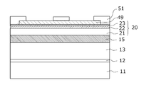
- Step S11 As shown in FIG. 5A, the reflective electrode 49 is formed at a predetermined position on the upper surface of the third semiconductor layer 23. Here, the case where the reflective electrode 49 is formed on the substantially entire area of the third semiconductor layer 23 inside the formation area of the third semiconductor layer 23 is shown.
- the reflective electrode 49 is formed by depositing Ni with a film thickness of 0.7 nm and Ag with a film thickness of 150 nm on the upper surface of the third semiconductor layer 23 with a sputtering apparatus and then using an RTA apparatus at 400 ° C. in a dry air atmosphere. Formed by performing contact annealing for 2 minutes.
- an alloy of Ni and Ag is adopted as a material of the reflective electrode 49, the reflective electrode 49 can also be formed of Al or Rh.
- Step S12 Next, as shown in FIG. 5B, the insulating layer 51 is formed in a predetermined portion of the upper layer of the reflective electrode 49. At this time, as shown in FIG. 5B, a part of the insulating layer 51 can be formed to cover the side surface of the reflective electrode 49.
- the upper layer of the reflective electrode 49 relating to the non-formation region of the insulating layer 51 is masked and, for example, SiO 2 is deposited to a film thickness of about 200 nm by a sputtering method.
- the material to be deposited may be an insulating material, and may be, for example, SiN or Al 2 O 3 .
- Step S13 As shown in FIG. 5C, the solder diffusion preventing layer 47 and the solder layer 45 are formed so as to cover the top surfaces of the reflective electrode 49 and the insulating layer 51.
- solder is formed by depositing Ti in a film thickness of 100 nm and Pt in a film thickness of 200 nm in three cycles so as to cover the upper surfaces of the reflective electrode 49 and the insulating layer 51 with an electron beam evaporation apparatus (EB apparatus).
- EB apparatus electron beam evaporation apparatus
- a diffusion prevention layer 47 is formed. After that, after depositing Ti with a film thickness of 10 nm on the upper surface (Pt surface) of the solder diffusion preventing layer 47, the solder layer is deposited by depositing Au-Sn solder composed of Au 80% Sn 20%.
- the solder layer 43 may be formed on the upper surface of the support substrate 9 prepared separately from the growth substrate 11 (see FIG. 5D).
- the solder layer 43 may be made of the same material as the solder layer 45, and the growth substrate 11 and the support substrate 9 are bonded by being bonded to the solder layer 43 in the next step.
- the support substrate 9 for example, CuW is used as described above in the section of the structure.
- the solder diffusion preventing layer 47 may be formed on the support substrate 9, and the solder layer 43 may be formed on the solder diffusion preventing layer 47.
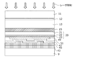
- Step S14 Next, as shown in FIG. 5E, the growth substrate 11 and the support substrate 9 are attached to each other. More specifically, the solder layer 47 formed on the upper layer of the growth substrate 11 and the solder layer 43 formed on the upper layer of the support substrate 9 are bonded together at a temperature of 280 ° C. and a pressure of 0.2 MPa.
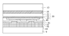
- Step S15 Next, as shown in FIG. 5F, the growth substrate 11 is peeled off. More specifically, with the growth substrate 11 facing up and the support substrate 9 facing down, the KrF excimer laser is irradiated from the growth substrate 11 side, and the interface between the growth substrate 11 and the semiconductor layer (undoped layer 12) To separate the growth substrate 11. The laser passes through the growth substrate 11 while the lower layer of GaN (the undoped layer 12) absorbs the laser, so that the interface is heated to decompose the GaN. Thus, the growth substrate 11 is peeled off.
- the GaN (undoped layer 12) remaining on the wafer is removed by wet etching using hydrochloric acid or the like or dry etching using an ICP apparatus, and the first semiconductor layer 13 is removed. Exposed.
- Step S16 Next, as shown in FIG. 5H, adjacent elements are separated. Specifically, the semiconductor layer (first semiconductor layer 13, active layer 15, fourth semiconductor layer 21, second semiconductor) until the upper surface of the insulating layer 51 is exposed using an ICP device with respect to the boundary region with the adjacent element The layer 22, the third semiconductor layer 23) is etched. At this time, the insulating layer 51 also functions as a stopper at the time of etching.
- an n-side electrode (72, 73) is formed on the top surface of the first semiconductor layer 13 at a position facing the insulating layer 51 in the direction perpendicular to the surface of the support substrate 9.
- sintering is performed at 250 ° C. for 1 minute in a nitrogen atmosphere.
- the respective elements are separated by, for example, a laser dicing apparatus, the back surface of the support substrate 9 is bonded to the package by, for example, Ag paste, and wire bonding is performed on the n-side electrode 73 as a feeding terminal.
- wire bonding is performed by connecting a wire 45 made of Au to a bonding area of 100 100 ⁇ m with a load of 50 g.
- the third semiconductor layer 23 made of p-GaN since the third semiconductor layer 23 made of p-GaN is provided, an Al-rich layer is not formed on the upper surface (the surface on the reflective electrode 49 side) of the second semiconductor layer 22 made of p-AlGaN. Therefore, the contact resistance does not rise due to the contact between the Al-rich layer and the reflective electrode 49.
- the third semiconductor layer 23 made of p-GaN can be made of an extremely thin film, it is absorbed by the third semiconductor layer 23 even when realizing a semiconductor light emitting element that emits ultraviolet light having a peak wavelength of 400 nm or less. Can be minimized to achieve high light output.
- the method of steps S11 to S17 is an example of a method of manufacturing a semiconductor light emitting device having a so-called “vertical structure”, and the present invention is limited to the semiconductor light emitting device manufactured by applying this method. is not.
- the first semiconductor layer 13 is composed of n-AlGaN, but n-Al x 1 Ga y 1 In 1-x 1-y N (0 ⁇ x1 ⁇ 1, 0 ⁇ y1 ⁇ 1) You may configure it.
- the second semiconductor layer 22 is constituted by p-AlGaN, configured in p-Al x2 Ga y2 In 1 -x2-y2 N (0 ⁇ x2 ⁇ 1,0 ⁇ y2 ⁇ 1) It does not matter.
- the fourth semiconductor layer 21 is made of p-AlGaN, but p-Al x 3 Ga y 3 In 1-x 3-y 3 N (0 ⁇ x 3 ⁇ 1, 0 ⁇ y 3 ⁇ 1) You may configure it.
- the third semiconductor layer 23 made of p-GaN may be completely evaporated through the cooling process according to step S8.
- step S8 p-Al x2 Ga y2 In 1-x2-y2 N second semiconductor layer 22 made of (0 ⁇ x2 ⁇ 1,0 ⁇ y2 ⁇ 1) is exposed
- the timing at which the second semiconductor layer 22 is exposed can be delayed by the time required for the third semiconductor layer 23 to completely evaporate as compared with the conventional light emitting element, it is included in the second semiconductor layer 22.
- the evaporation amount of GaN can be suppressed.
- the Al-rich layer formed on the upper surface of the second semiconductor layer 22 can be extremely reduced as compared to the conventional light emitting element, so that the operating voltage lower than that of the conventional light emitting element can be realized.
- SYMBOLS 1 Semiconductor light emitting element of the present invention 9: Support substrate 11: Growth substrate 12: Undoped layer 13: First semiconductor layer (n-type semiconductor layer) 15: Active layer 20: p-type semiconductor layer 21: fourth semiconductor layer (p-type semiconductor layer) 22: Second semiconductor layer (p-type semiconductor layer) 23: Third semiconductor layer (p-type semiconductor layer) 31: n-side electrode 32: p-side electrode 35: Al rich layer 43, 45: solder layer 47: solder diffusion preventing layer 49: reflective electrode 51: insulating layer 72, 73: n-side electrode 100: conventional semiconductor light emitting device 101: Substrate 102: Buffer layer 103: n-type contact layer 104: n-type cladding layer 105: active layer 106: p-type cladding layer 107: first p-type contact layer 108: second p-type contact layer 109: n Side electrode 110: p side electrode
Landscapes
- Led Devices (AREA)
Abstract
動作電圧を従来よりも低下させながらも高い光出力を得ることのできる半導体発光素子及びその製造方法を実現する。 本発明に係る半導体発光素子の製造方法は、基板を準備する工程(a)、基板上に、n-Alx1Gay1In1-x1-y1N(0≦x1≦1,0≦y1≦1)よりなるn型の第一半導体層を形成する工程(b)、第一半導体層の上層に活性層を形成する工程(c)、活性層の上層に、炉内の温度を800℃以上としてp-Alx2Gay2In1-x2-y2N(0<x2≦1,0≦y2<1)よりなるp型の第二半導体層を形成する工程(d)、第二半導体層の上層に、前記炉内の温度を800℃以上としてp-GaNよりなるp型の第三半導体層を形成する工程(e)、及び、工程(e)の後に炉内温度を低下させる工程(f)を有する。
Description
本発明は半導体発光素子及びその製造方法に関する。
窒化物半導体を用いた発光素子として、下記特許文献1の構造が知られている。図6は、同文献に開示されている半導体発光素子の構造を模式的に示す断面図である。
図6に示す従来の半導体発光素子100は、基板101、バッファ層102、n型コンタクト層103、n型クラッド層104,活性層105、p型クラッド層106、第一のp型コンタクト層107、第二のp型コンタクト層108を備える。また、半導体発光素子100は、n型コンタクト層103の上面にn側電極109を有し、第二のp型コンタクト層108の上面にp側電極110を有する。
特許文献1によれば、p側電極110と接触する第二のp型コンタクト層108はp型不純物濃度が高くAl組成比の低い半導体層で構成され、第一のp型コンタクト層107は第二のp型コンタクト層108と比較してp型不純物濃度が低くAl組成比の高い半導体層で構成されると記載されている。同文献によれば、このようにp型不純物濃度とAl組成比が異なる2種類の層でp型コンタクト層(107,108)を形成することにより、p側電極110とのオーミック接触を実現しながらも、自己吸収を防止しながら素子特性を維持できる程度にコンタクト層の膜厚を確保することができると記載されている。
特許文献1によれば、図6に示す従来の半導体発光素子100は以下の手順で作製される。
基板101の上層にGaNよりなるバッファ層102を510℃で成長させた後、n型Al0.04Ga0.96Nよりなるn型コンタクト層103を1050℃で成長させる。次に、n型コンタクト層103の上層にn型Al0.18Ga0.82Nよりなるn型クラッド層104を1050℃で成長させ、その後に700℃でアンドープInGaNよりなる活性層105を成長させる。なお、本明細書において、InGaNとの記載は、Ina1Ga1-a1N(0<a1<1)という意味であり、InとGaの組成比が1:1であることを表すものではない。AlGaN等の記載も同趣旨である。
次に、1050℃で、Al0.2Ga0.8Nよりなるp型クラッド層106を成長させる。次に、p型クラッド層106上にMgを1×10¹⁹/cm3ドープしたAl0.04Ga0.96Nよりなる第一のp型コンタクト層107を0.1μmの膜厚で成長させた後、ガスの流量を調整してMgを2×1021/cm3ドープしたAl0.01Ga0.99Nよりなる第二のp型コンタクト層108を0.02μmの膜厚で成長させる。
その後、ウェハを反応容器内において、700℃でアニーリングを行い、p型半導体層を低抵抗化した後、ウェハを反応容器から取り出す。そして、最上層に位置する第二のp型コンタクト層108の表面に所定の形状のマスクを形成し、RIE(反応性イオンエッチング)装置で第二のp型コンタクト層108側から半導体層をエッチングして、図6に示すようにn型コンタクト層103の表面を露出させる。そして、露出したn型コンタクト層103の上面にn側電極109を形成し、第二のp型コンタクト層108の上面にp側電極110を形成する。
ここで、上述したように、p型クラッド層106、第一のp型コンタクト層107、及び第二のp型コンタクト層108は、いずれも炉内を1000℃以上の高温状態としてエピタキシャル成長させることで形成される。その後、炉内の温度は低下される。上記の方法では、700℃程度まで低下されてアニール処理が施された後、ウェハは炉外へと出される。
しかし、本発明者の鋭意研究によれば、上述した方法によって製造された半導体発光素子は、動作電圧が高くなることを見出した。
本発明は、上記の課題に鑑み、動作電圧を従来よりも低下させながらも高い光出力を得ることのできる半導体発光素子及びその製造方法を実現することを目的とする。
本発明者は、鋭意研究により、特許文献1に記載された半導体発光素子の動作電圧が高くなる理由を以下のように考えている。
特許文献1に記載された半導体発光素子100の半導体層のうち最上面に位置する半導体層、すなわちp側電極110と接触する半導体層(第二のp型コンタクト層108)は、Al0.01Ga0.99Nで構成されている。そして、この層は、炉内の温度を1050℃という高温にした状態でエピタキシャル成長することで形成された層である。
ところで、AlGaNはGaNとAlNの混晶であり、AlNの形成温度はGaNの形成温度よりも高い。つまり、1050℃という高温下でTMG(トリメチルガリウム)、TMA(トリメチルアルミニウム)、アンモニア等の原料ガスを供給しながらAlGaNからなる第二のp型コンタクト層108を成長させた後、ガスの供給を停止しても、炉内はしばらくの間、極めて高い温度下に晒される。このとき、第二のp型コンタクト層108を構成するAlGaNのうちのGaNが選択的に蒸発してしまい、AlGaNのAl組成比が高まる。
つまり、成長条件としては、Al0.01Ga0.99Nが形成されるように各原料ガスの流量比を設定していたとしても、ガスの供給を停止してから、GaNが蒸発しない程度に炉内が低温になるまでの間、特に第二のp型コンタクト層108の上面からGaNが蒸発してしまう。このため、第二のp型コンタクト層108の上面にはAlリッチの層が形成される。
このように第二のp型コンタクト層108の上面にAlリッチの層が存在すると、当該層のバンドギャップが拡がり、キャリア濃度が下がってしまう。また、Alリッチの層が酸化してAl2O3等の高抵抗層が表面に形成される場合がある。これらの理由により、p側電極110と第二のp型コンタクト層108との間のコンタクト抵抗が高くなり、半導体発光素子100の動作電圧が上昇してしまう。
かかる考察の下、本発明に係る半導体発光素子の製造方法は、
基板を準備する工程(a)、
前記基板上に、n-Alx1Gay1In1-x1-y1N(0≦x1≦1,0≦y1≦1)よりなるn型の第一半導体層を形成する工程(b)、
前記第一半導体層の上層に活性層を形成する工程(c)、
前記活性層の上層に、炉内の温度を800℃以上としてp-Alx2Gay2In1-x2-y2N(0<x2≦1,0≦y2<1)よりなるp型の第二半導体層を形成する工程(d)、
前記第二半導体層の上層に、前記炉内の温度を800℃以上としてp-GaNよりなるp型の第三半導体層を形成する工程(e)、
及び、前記工程(e)の後に炉内温度を低下させる工程(f)を有することを特徴とする。
基板を準備する工程(a)、
前記基板上に、n-Alx1Gay1In1-x1-y1N(0≦x1≦1,0≦y1≦1)よりなるn型の第一半導体層を形成する工程(b)、
前記第一半導体層の上層に活性層を形成する工程(c)、
前記活性層の上層に、炉内の温度を800℃以上としてp-Alx2Gay2In1-x2-y2N(0<x2≦1,0≦y2<1)よりなるp型の第二半導体層を形成する工程(d)、
前記第二半導体層の上層に、前記炉内の温度を800℃以上としてp-GaNよりなるp型の第三半導体層を形成する工程(e)、
及び、前記工程(e)の後に炉内温度を低下させる工程(f)を有することを特徴とする。
上記の方法とすることで、炉内の温度が低下する直前の状態、すなわち工程(f)の直前の状態で、p-Alx2Gay2In1-x2-y2N(0<x2≦1,0≦y2<1)よりなるp型の第二半導体層の上面にはp-GaNよりなるp型の第三半導体層が形成されている。つまり、炉内の温度が高温の状態でガスの供給を停止しても、Alを含む混晶で構成される第二半導体層は最上面に位置していないため、この第二半導体層からGaNが蒸発して第二半導体層の上面がAlリッチになるということはない。また、ガスの供給を停止した時点で最上面に位置している第三半導体層はp-GaNで構成されているため、炉内の温度を低下させている工程中に第三半導体層からGaNが蒸発したとしても、Alリッチな層が第三半導体層の最上面に形成されるということはない。
従って、従来のように、p側電極と接触するp型半導体層の上面にAlリッチな層が形成されていないため、炉内温度を低下させる工程(f)の後に第三半導体層の上面にp側電極を形成しても、p側電極と第三半導体層の間のコンタクト抵抗が高くなるということがない。よって、従来よりも動作電圧の低い半導体発光素子が実現される。この結果は、「発明を実施するための形態」の項で実施例を参照して後述される。
なお、第三半導体層は、ドープされているp型不純物濃度が高い(例えば1×10¹⁹/cm3以上)層としても構わない。
また、第二半導体層についても、ドープされているp型不純物濃度が高い(例えば1×10¹⁹/cm3以上)層としても構わない。この場合、工程(f)の過程において、第三半導体層が全て蒸発してしまっても構わない。このとき、第三半導体層は、第二半導体層を構成するAlを含む混晶からGaNの蒸発を防ぐための保護層としてのみ機能する。そして、工程(f)の後、第二半導体層の上面にp側電極が形成される。この場合、p側電極と接触する半導体層は、p-Alx2Gay2In1-x2-y2Nからなる第二半導体層である。この第二半導体層がAlGaN層である場合には、p-AlGaN層の上層にp側電極が形成されている点に関しては、図6を参照して上述した従来の構造と同様である。しかし、上述したように、第二半導体層は、工程(f)の後、特に炉内温度が高い初期段階においては、その上面に保護層としての第三半導体層が形成されているため、従来構成とは異なり、p-Alx2Gay2In1-x2-y2Nからなる第二半導体層の上面にはAlリッチな層が形成されない。よって、従来の構成よりも動作電圧の低い半導体発光素子が実現される。
なお、工程(d)は、p-Alx2Gay2In1-x2-y2N(0<x2≦1,0≦y2<1)を成長することのできる温度以上の温度で形成するものとして構わない。同様に、工程(e)は、p-GaNを成長することのできる温度以上の温度で形成するものとして構わない。
また、本発明の半導体発光素子の製造方法は、前記工程(f)の後に前記第三半導体層の上層に電極を形成する工程(g)を更に有するものとして構わない。
また、前記工程(e)は、前記工程(d)と比べて、前記炉内に供給される原料ガスの流量のみが変更されて実行される工程とすることもできる。すなわち、工程(d)と工程(e)とで成長温度をほぼ同じとしても構わない。
このとき、工程(e)は工程(d)に引き続き炉内を高い温度として半導体層を成長させる工程であるため、工程(d)によって形成されたp-Alx2Gay2In1-x2-y2N(0<x2≦1,0≦y2<1)よりなる第二半導体層の上面からGaNが蒸発してAlリッチの層が上面に形成されるということはなく、第二半導体層の上面に第三半導体層が形成される。
また、前記工程(f)の実行後、前記第三半導体層の膜厚が5nm以下となっていても構わない。
特に、半導体発光素子をピーク波長が400nm以下の紫外光を放射する素子として実現する場合には、吸収端がAlNよりも長波長側に位置するGaNからなる半導体層はできるだけ薄くするのが好ましい。上述したように、第三半導体層は、第二半導体層の上面にAlリッチな層を形成しないようにするための保護層として機能させる目的で設けられているため、工程(e)の実行後、炉内の温度がまだ高い状態の下で第二半導体層の上面を覆っていればよい。
そして、工程(e)の実行後、工程(f)を開始する初期段階では、ガスの供給が停止された状態で炉内の温度が高いため、p-GaNで構成された第三半導体層の一部が蒸発する。このため、工程(f)の実行後における第三半導体層の膜厚は、工程(e)で形成された膜厚よりは薄膜化される。工程(e)において、工程(f)の実行後にp-GaNからなる第三半導体層の膜厚が5nm以下となるように、前記第三半導体層の成長膜厚を設定することで、光出力の高い紫外光発光素子を実現することができる。
また、前記工程(c)の後、前記活性層の上層に、炉内の温度を800℃以上としてp-Alx3Gay3In1-x3-y3N(0<x3≦1,0≦y3<1)よりなるp型の第四半導体層を形成する工程(h)を有し、
前記工程(d)は、前記工程(h)の後に実行され、前記第四半導体層よりもp型不純物濃度が高濃度である前記第二半導体層を形成する工程であるものとしても構わない。
前記工程(d)は、前記工程(h)の後に実行され、前記第四半導体層よりもp型不純物濃度が高濃度である前記第二半導体層を形成する工程であるものとしても構わない。
この場合、第四半導体層がp型クラッド層を構成し、第二半導体層がp型コンタクト層を構成するものとすることができる。なお、工程(f)の実行後において第三半導体層が残存している場合には、第二半導体層及び第三半導体層がp型コンタクト層を構成するものとすることができる。
本発明は、基板上に、n型半導体層と、p型半導体層と、前記n型半導体層及び前記p型半導体層の間に挟持された活性層とを有し、ピーク波長が400nm以下の紫外光を放射する半導体発光素子であって、
前記p型半導体層は、p-Alx2Gay2In1-x2-y2N(0<x2≦1,0≦y2<1)よりなるp型の第二半導体層と、膜厚5nm以下のp-GaNよりなるp型の第三半導体層とを含み、
前記第三半導体層は、前記p型半導体層の面のうち、前記活性層とは反対側の面の最上層であることを特徴とする。
前記p型半導体層は、p-Alx2Gay2In1-x2-y2N(0<x2≦1,0≦y2<1)よりなるp型の第二半導体層と、膜厚5nm以下のp-GaNよりなるp型の第三半導体層とを含み、
前記第三半導体層は、前記p型半導体層の面のうち、前記活性層とは反対側の面の最上層であることを特徴とする。
第三半導体層はp-GaNで構成されているが、膜厚5nm以下であるため、ピーク波長が400nm以下の紫外光発光素子として実現した場合においても、第三半導体層内において吸収される光の量を極めて少なくすることができる。
窒化物半導体を用いて、ピーク波長が400nm以下の紫外光発光素子を実現しようとする場合、吸収端がAlNより長波長側に位置するGaNは極力利用しないのが好ましいとされているため、Alを含む窒化物半導体層で全ての半導体層を構成することが通常考えられる。
しかし、上記構成に係る半導体発光素子は、p型半導体層の最上面に位置する層に敢えてp-GaNからなる第三半導体層を備えている。より具体的に言えば、p側電極と接触する位置に形成される層をp-GaNからなる第三半導体層とすることができることを意味している。
上述したように、p側電極と接触する位置に形成される半導体層、例えばp型コンタクト層を、AlGaNやAlInGaN等のAlを含む半導体層で構成した場合、炉内において各半導体層を形成させるためのエピタキシャル成長工程が完了して原料ガスの供給を停止してから、炉内温度が低下する過程の間にGaNが蒸発し、その上面にAlリッチな層が形成されてしまう。この結果、当該層とp側電極との間のコンタクト抵抗が上昇してしまう。上記構成によれば、p型半導体層の最上面がp-GaNからなる第三半導体層であるため、当該層の上面にAlリッチの層が形成されず、p側電極との間のコンタクト抵抗を低抵抗化することができる。これにより、従来の半導体発光素子よりも動作電圧を低下させることができる。
また、本発明の半導体発光素子は、前記第三半導体層の上層に電極を有しているものとしても構わない。より詳細には、前記第三半導体層の面のうち、前記活性層とは反対側の面上に電極を有する構成とすることができる。
また、前記p型半導体層は、p-Alx3Gay3In1-x3-y3N(0<x3≦1,0≦y3<1)よりなるp型の第四半導体層と、前記第四半導体層の上層に形成された前記第二半導体層と、前記第二半導体層の上層に形成された前記第三半導体層とを有するものとすることもできる。
上記構成において、第二半導体層及び第三半導体層は、第四半導体層よりもp型不純物濃度を高濃度にするものとしても構わない。この場合、第四半導体層がp型クラッド層を構成し、第二半導体層がp型コンタクト層を構成するものとすることができる。
また、前記n型半導体層は、n-Alx1Gay1In1-x1-y1N(0≦x1≦1,0≦y1≦1)よりなるn型の第一半導体層で構成されているものとしても構わない。
本発明によれば、従来よりも動作電圧を低下させながらも高い光出力を得ることのできる半導体発光素子を実現することができる。
本発明の半導体発光素子及びその製造方法につき、図面を参照して説明する。なお、各図において図面の寸法比と実際の寸法比は必ずしも一致しない。
まず、以下では、本発明の半導体発光素子の構造について説明をした後、その製造方法について説明する。その後、実施例を参照して、本発明の半導体発光素子と従来の半導体発光素子との性能を比較する。
[構造]
図1は、本発明の半導体発光素子の一実施形態の構成を模式的に示す断面図である。半導体発光素子1は、成長基板11上に、n型半導体層13と、p型半導体層20と、n型半導体層13及びp型半導体層20の間に挟持された活性層15とを有する。より詳細な半導体発光素子1の構成について、以下説明する。
図1は、本発明の半導体発光素子の一実施形態の構成を模式的に示す断面図である。半導体発光素子1は、成長基板11上に、n型半導体層13と、p型半導体層20と、n型半導体層13及びp型半導体層20の間に挟持された活性層15とを有する。より詳細な半導体発光素子1の構成について、以下説明する。
図1に示す半導体発光素子1は、成長基板11上にアンドープ層12を有し、アンドープ層の上層にn型半導体層13を有する。そして、半導体発光素子1は、n型半導体層13の上層に活性層15を有し、活性層15の上層にp型半導体層20を有する。図1に示す半導体発光素子1においては、p型半導体層20が、p型半導体層21、p型半導体層22、及びp型半導体層23を有して構成されている。
なお、n型半導体層13が「第一半導体層」に対応し、p型半導体層21が「第四半導体層」に対応し、p型半導体層22が「第二半導体層」に対応し、p型半導体層23が「第三半導体層」に対応する。以下では、n型半導体層13を「第一半導体層13」と称し、p型半導体層21を「第四半導体層21」と称し、p型半導体層22を「第二半導体層22」と称し、p型半導体層23を「第三半導体層23」と称する。
つまり、半導体発光素子1においては、第三半導体層23が、p型半導体層20の面のうち、活性層15とは反対側の面の最上層を構成している。
(成長基板11)
成長基板11は一例としてサファイア基板で構成される。なお、成長基板11は、サファイアの他、Si、SiC、AlN、AlGaN、GaN、YAGなどで構成しても構わない。
成長基板11は一例としてサファイア基板で構成される。なお、成長基板11は、サファイアの他、Si、SiC、AlN、AlGaN、GaN、YAGなどで構成しても構わない。
(アンドープ層12)
アンドープ層12は、GaNにて形成される。より具体的には、GaNよりなる低温バッファ層と、その上層にGaNよりなる下地層によって形成される。このアンドープ層12は、例えばサファイアで構成される成長基板11の上層に、第一半導体層13等を良好な状態でエピタキシャル成長させるために設けられているものである。
アンドープ層12は、GaNにて形成される。より具体的には、GaNよりなる低温バッファ層と、その上層にGaNよりなる下地層によって形成される。このアンドープ層12は、例えばサファイアで構成される成長基板11の上層に、第一半導体層13等を良好な状態でエピタキシャル成長させるために設けられているものである。
(第一半導体層13)
第一半導体層13はn-Alx1Gay1In1-x1-y1N(0≦x1≦1,0≦y1≦1)によって構成される。第一半導体層13は、Si,Ge,S,Se,Sn,Teなどのn型不純物がドープされており、特にSiがドープされているのが好ましい。本実施形態では、一例として第一半導体層13をn-Al0.06Ga0.94Nで形成している。
第一半導体層13はn-Alx1Gay1In1-x1-y1N(0≦x1≦1,0≦y1≦1)によって構成される。第一半導体層13は、Si,Ge,S,Se,Sn,Teなどのn型不純物がドープされており、特にSiがドープされているのが好ましい。本実施形態では、一例として第一半導体層13をn-Al0.06Ga0.94Nで形成している。
(活性層15)
活性層15は、例えばInGaNからなる発光層とAlGaNからなる障壁層が周期的に繰り返されて構成される。これらの層はアンドープでもp型又はn型にドープされていても構わない。
活性層15は、例えばInGaNからなる発光層とAlGaNからなる障壁層が周期的に繰り返されて構成される。これらの層はアンドープでもp型又はn型にドープされていても構わない。
なお、活性層15は、上記の材料に限らず、第一の窒化物半導体層と、この第一の窒化物半導体層よりもバンドギャップの大きい第二の窒化物半導体層とを有し、第一の窒化物半導体層が2つの第二の窒化物半導体層で挟持される構成を有していればよい。この場合、第一の窒化物半導体層が発光層を構成し、第二の窒化物半導体層が障壁層を構成する。活性層15を構成する各材料は、取り出したい光のピーク波長に応じて適宜選択される。
(第四半導体層21)
第四半導体層21はp-Alx3Gay3In1-x3-y3N(0<x3≦1,0≦y3<1)によって構成される。第四半導体層21は、Mg、Be、Zn、又はCなどのp型不純物がドープされており、特にMgがドープされているのが好ましい。本実施形態では、一例として第四半導体層21をp-Al0.3Ga0.7Nとp-Al0.13Ga0.87Nの積層構造で形成している。
第四半導体層21はp-Alx3Gay3In1-x3-y3N(0<x3≦1,0≦y3<1)によって構成される。第四半導体層21は、Mg、Be、Zn、又はCなどのp型不純物がドープされており、特にMgがドープされているのが好ましい。本実施形態では、一例として第四半導体層21をp-Al0.3Ga0.7Nとp-Al0.13Ga0.87Nの積層構造で形成している。
(第二半導体層22)
第二半導体層22はp-Alx2Gay2In1-x2-y2N(0<x2≦1,0≦y2<1)によって構成される。第二半導体層22は、Mg、Be、Zn、又はCなどのp型不純物がドープされており、特にMgがドープされているのが好ましい。本実施形態では、一例として第二半導体層22をp-Al0.13Ga0.87Nで形成している。また、本実施形態では、第二半導体層22のp型不純物濃度は、第四半導体層21のp型不純物濃度よりも高濃度である。
第二半導体層22はp-Alx2Gay2In1-x2-y2N(0<x2≦1,0≦y2<1)によって構成される。第二半導体層22は、Mg、Be、Zn、又はCなどのp型不純物がドープされており、特にMgがドープされているのが好ましい。本実施形態では、一例として第二半導体層22をp-Al0.13Ga0.87Nで形成している。また、本実施形態では、第二半導体層22のp型不純物濃度は、第四半導体層21のp型不純物濃度よりも高濃度である。
(第三半導体層23)
第三半導体層23は膜厚が5nm以下のp-GaNによって構成される。第三半導体層23は、Mg、Be、Zn、又はCなどのp型不純物がドープされており、特にMgがドープされているのが好ましい。
第三半導体層23は膜厚が5nm以下のp-GaNによって構成される。第三半導体層23は、Mg、Be、Zn、又はCなどのp型不純物がドープされており、特にMgがドープされているのが好ましい。
本実施形態では、第三半導体層23のp型不純物濃度は、第四半導体層21のp型不純物濃度よりも高濃度である。一例として、第四半導体層21のp型不純物濃度は3×10¹⁹/cm3程度であり、第二半導体層22及び第三半導体層23のp型不純物濃度は1×1020/cm3程度である。
なお、製造方法の項で後述するように、ステップS7に係る工程において第三半導体層23を所定の膜厚だけ形成した後、ステップS8に係る冷却工程を経ることで、第三半導体層23の一部が蒸発して膜厚が薄くなる。図1において、第三半導体層23の上層を破線で示しているのは、第三半導体層23を形成した後に膜厚が減少していることを表すためである。すなわち、図1では、ステップS8の工程において、破線部分に相当する第三半導体層23が蒸発したことを表している。
なお、上述した実施形態では、半導体発光素子1が図1に示すような構造である場合について説明したが、半導体発光素子1は必ずしも第四半導体層21を備えなくても構わない。すなわち、半導体発光素子1は、活性層15の上面に第二半導体層22を備える構成であっても構わない。
また、半導体発光素子1が第四半導体層21を備える場合において、必ずしも第二半導体層22のp型不純物濃度を第四半導体層21のp型不純物濃度より高くしなければならないものでもない。
[製造方法]
次に、半導体発光素子1の製造方法について説明する。なお、以下で説明する製造条件や膜厚等の寸法はあくまで一例であって、これらの数値に限定されるものではない。
次に、半導体発光素子1の製造方法について説明する。なお、以下で説明する製造条件や膜厚等の寸法はあくまで一例であって、これらの数値に限定されるものではない。
(ステップS1)
成長基板11を準備する。より具体的には、成長基板11としてc面サファイア基板を準備して、これに対してクリーニングを行う。このクリーニングは、より具体的には、例えばMOCVD(Metal Organic Chemical Vapor Deposition:有機金属化学気相蒸着)装置の処理炉内に成長基板11(c面サファイア基板)を配置し、処理炉内に流量が10slmの水素ガスを流しながら、炉内温度を例えば1150℃に昇温することにより行われる。
成長基板11を準備する。より具体的には、成長基板11としてc面サファイア基板を準備して、これに対してクリーニングを行う。このクリーニングは、より具体的には、例えばMOCVD(Metal Organic Chemical Vapor Deposition:有機金属化学気相蒸着)装置の処理炉内に成長基板11(c面サファイア基板)を配置し、処理炉内に流量が10slmの水素ガスを流しながら、炉内温度を例えば1150℃に昇温することにより行われる。
本ステップS1が工程(a)に対応する。
(ステップS2)
成長基板11の表面に、GaNよりなる低温バッファ層を形成し、更にその上層にGaNよりなる下地層を形成する。これらの低温バッファ層及び下地層がアンドープ層12に対応する。
成長基板11の表面に、GaNよりなる低温バッファ層を形成し、更にその上層にGaNよりなる下地層を形成する。これらの低温バッファ層及び下地層がアンドープ層12に対応する。
具体的なアンドープ層12の形成方法は、例えば以下の通りである。まず、МОCVD装置の炉内圧力を100kPa、炉内温度を480℃とする。そして、処理炉内にキャリアガスとして流量がそれぞれ5slmの窒素ガス及び水素ガスを流しながら、原料ガスとして、流量が50μmol/minのTMG及び流量が250000μmol/minのアンモニアを処理炉内に68秒間供給する。これにより、成長基板11の表面に、厚みが20nmのGaNよりなる低温バッファ層を形成する。
次に、MOCVD装置の炉内温度を1150℃に昇温する。そして、処理炉内にキャリアガスとして流量が20slmの窒素ガス及び流量が15slmの水素ガスを流しながら、原料ガスとして、流量が100μmol/minのTMG及び流量が250000μmol/minのアンモニアを処理炉内に30分間供給する。これにより、低温バッファ層の表面に、厚みが1.7μmのGaNよりなる下地層を形成する。
本ステップS2により、図2Aに示すように、成長基板11上にアンドープ層12が形成される。
(ステップS3)
次に、図2Bに示すように、アンドープ層12の上層にn型の第一半導体層13を形成する。第一半導体層13の具体的な形成方法は、例えば以下の通りである。
次に、図2Bに示すように、アンドープ層12の上層にn型の第一半導体層13を形成する。第一半導体層13の具体的な形成方法は、例えば以下の通りである。
まず、引き続き炉内温度を1150℃とした状態で、MOCVD装置の炉内圧力を30kPaとする。そして、処理炉内にキャリアガスとして流量が20slmの窒素ガス及び流量が15slmの水素ガスを流しながら、原料ガスとして、流量が94μmol/minのTMG、流量が6μmol/minのTMA、流量が250000μmol/minのアンモニア及び流量が0.013μmol/minのテトラエチルシランを処理炉内に60分間供給する。これにより、例えばn-Al0.06Ga0.94Nの組成を有し、Si濃度が5×1019/cm3で、厚みが2μmの第一半導体層13がアンドープ層12の上層に形成される。
ここでは、第一半導体層13にドープされるn型不純物をSiとする場合について説明したが、n型不純物としては、Si以外にGe、S、Se、Sn又はTe等を用いることができる。
なお、この後、TMAの供給を停止すると共に、それ以外の原料ガスを6秒間供給することにより、第一半導体層13の上層に厚みが5nm程度のn-GaNを形成しても構わない。
本ステップS3が工程(b)に対応する。
(ステップS4)
次に、図2Cに示すように、n型の第一半導体層13の上層に、例えばInGaNで構成される発光層及びn-AlGaNで構成される障壁層が周期的に繰り返されてなる活性層15を形成する。
次に、図2Cに示すように、n型の第一半導体層13の上層に、例えばInGaNで構成される発光層及びn-AlGaNで構成される障壁層が周期的に繰り返されてなる活性層15を形成する。
具体的には、まずMOCVD装置の炉内圧力を100kPa、炉内温度を830℃とする。そして、処理炉内にキャリアガスとして流量が15slmの窒素ガス及び流量が1slmの水素ガスを流しながら、原料ガスとして、流量が10μmol/minのTMG、流量が12μmol/minのトリメチルインジウム(TMI)及び流量が300000μmol/minのアンモニアを処理炉内に48秒間供給するステップを行う。その後、流量が10μmol/minのTMG、流量が1.6μmol/minのTMA、0.002μmol/minのテトラエチルシラン及び流量が300000μmol/minのアンモニアを処理炉内に120秒間供給するステップを行う。以下、これらの2つのステップを繰り返すことにより、厚みが2nmのInGaNよりなる発光層及び厚みが7nmのn-AlGaNよりなる障壁層が15周期繰り返されてなる活性層15が、第一半導体層13の上層に形成される。
本ステップS4が工程(c)に対応する。
(ステップS5)
次に、図2Dに示すように、活性層15の上層にp型の第四半導体層21を形成する。第四半導体層21の具体的な形成方法は、例えば以下の通りである。
次に、図2Dに示すように、活性層15の上層にp型の第四半導体層21を形成する。第四半導体層21の具体的な形成方法は、例えば以下の通りである。
MOCVD装置の炉内圧力を100kPaに維持し、処理炉内にキャリアガスとして流量が15slmの窒素ガス及び流量が25slmの水素ガスを流しながら、炉内温度を1025℃に昇温する。その後、原料ガスとして、流量が35μmol/minのTMG、流量が20μmol/minのTMA、流量が250000μmol/minのアンモニア及びp型不純物をドープするための流量が0.1μmol/minのビスシクロペンタジエニルマグネシウム(Cp2Mg)を処理炉内に60秒間供給する。これにより、活性層15の表面に、厚みが20nmのAl0.3Ga0.7Nの組成を有する正孔供給層を形成する。その後、TMAの流量を4μmol/minに変更して原料ガスを360秒間供給することにより、厚みが120nmのAl0.13Ga0.87Nの組成を有する正孔供給層を形成する。これらの正孔供給層により第四半導体層21が形成される。この第四半導体層21のp型不純物濃度は、例えば3×1019/cm3程度である。
なお、ここでは炉内の温度を1025℃として第四半導体層21を形成したが、p型不純物をドープしながらAlGaNを成長できる下限温度以上(例えば800℃以上)の温度であれば1025℃に限定されるものではない。ただし、成長温度は900℃以上であれば好ましく、1000℃以上であればより好ましい。
本ステップS5が工程(h)に対応する。
(ステップS6)
次に、図2Eに示すように、p型の第四半導体層21の上層にp型の第二半導体層22を形成する。第二半導体層22の具体的な形成方法は、例えば以下の通りである。
次に、図2Eに示すように、p型の第四半導体層21の上層にp型の第二半導体層22を形成する。第二半導体層22の具体的な形成方法は、例えば以下の通りである。
ステップS5から引き続き炉内の温度及びキャリアガスの流量を維持したまま、原料ガスとして、流量が20μmol/minのTMG、流量が4μmol/minのTMA、流量が250000μmol/minのアンモニア及びp型不純物をドープするための流量が0.2μmol/minのCp2Mgを処理炉内に40秒間供給する。これにより、第四半導体層21の上層に、厚みが10nmのp-Al0.13Ga0.87Nの組成を有する第二半導体層22が形成される。この第二半導体層22のp型不純物濃度は、例えば1×1020/cm3程度である。
本ステップS6が工程(d)に対応する。
(ステップS7)
次に、図2Fに示すように、p型の第二半導体層22の上層にp型の第三半導体層23を形成する。第三半導体層23の具体的な形成方法は、例えば以下の通りである。
次に、図2Fに示すように、p型の第二半導体層22の上層にp型の第三半導体層23を形成する。第三半導体層23の具体的な形成方法は、例えば以下の通りである。
ステップS6から引き続き炉内の温度を維持した状態で、TMAの供給を停止すると共に、Cp2Mgの流量を0.2μmol/minに変更して原料ガスを20秒間供給する。これにより、第二半導体層22の上層に、厚みが5nm程度のp-GaNからなる第三半導体層23が形成される。この第三半導体層23のp型不純物濃度は、例えば1×1020/cm3程度である。
本ステップS7が工程(e)に対応する。
(ステップS8)
次に、所定の原料ガスの供給を停止して炉内の温度を低下させる。本ステップS8が工程(f)に対応する。
次に、所定の原料ガスの供給を停止して炉内の温度を低下させる。本ステップS8が工程(f)に対応する。
炉内の温度を低下させる本ステップS8の開始直前の状態では、p-AlGaNで構成された第二半導体層22の上面にはp-GaNよりなるp型の第三半導体層23が形成されている。つまり、炉内の温度が高温の状態でガスの供給を停止しても、Alを含む混晶で構成される第二半導体層22は最上面に位置していないため、この第二半導体層22からGaNが蒸発して第二半導体層22の上面がAlリッチになるということはない。
また、原料ガスの供給を停止した時点でp型半導体層20の最上面に位置している第三半導体層23はp-GaNで構成されているため、炉内の温度を低下させている工程中に第三半導体層23からGaNが蒸発したとしても、Alリッチな層が第三半導体層23の最上面に形成されるということはない。
ステップS7の完了後、原料ガスの供給を停止して炉内温度を低下させる過程において、第三半導体層23を構成するp-GaNの少なくとも一部が蒸発し、第三半導体層23の膜厚は薄くなる。一例では、本ステップS8の完了時点において、第三半導体層23の膜厚が1nm以下となる。上述したように、第三半導体層23の膜厚は、ステップS8の完了時点において、ステップS7の完了時点よりも薄くなっており、図1では破線によってこのことを表している。
なお、このステップS8において、炉内の温度が700℃程度に低下するまでの間はアンモニアを流し、700℃程度まで低下した後は、炉内の温度が室温程度に低下するまでの間窒素ガスのみを炉内に供給するものとしても構わない。このようにすることで、炉内の冷却工程において、ウェハの活性化処理を行うことができる。
(以後の工程)
ステップS8の後、処理炉からウェハを取り出し、通電のための電極を形成する工程(工程(g)に対応する。)を行う。具体的には以下の方法で行われる。
ステップS8の後、処理炉からウェハを取り出し、通電のための電極を形成する工程(工程(g)に対応する。)を行う。具体的には以下の方法で行われる。
(ステップS9)
図2Gに示すように、第一半導体層13の一部上面が露出するまで、一部領域のp型半導体層20(第三半導体層23、第二半導体層22、及び第四半導体層21)及び活性層15を、ICP装置を用いたドライエッチングによって除去する。なお、本ステップS9において、第一半導体層13についても一部エッチング除去しても構わない。
図2Gに示すように、第一半導体層13の一部上面が露出するまで、一部領域のp型半導体層20(第三半導体層23、第二半導体層22、及び第四半導体層21)及び活性層15を、ICP装置を用いたドライエッチングによって除去する。なお、本ステップS9において、第一半導体層13についても一部エッチング除去しても構わない。
(ステップS10)
図2Hに示すように、第一半導体層13の上面にn側電極31を形成し、p型半導体層20の上面、より詳細には第三半導体層23の上面にp側電極32を形成する。具体的な形成方法は、例えば以下の通りである。
図2Hに示すように、第一半導体層13の上面にn側電極31を形成し、p型半導体層20の上面、より詳細には第三半導体層23の上面にp側電極32を形成する。具体的な形成方法は、例えば以下の通りである。
第一半導体層13の上面の少なくとも一部の領域に、例えば膜厚100nmのCrと膜厚0.5~3μmのAuを蒸着した後、窒素雰囲気中で250℃、1分間程度のアニール処理を行う。これにより、第一半導体層13の上面にn側電極31が形成される。
また、第三半導体層23の少なくとも一部の上面に導電性材料で構成された材料膜を成膜する。例えばスパッタ装置にて第三半導体層23の上面の所定の領域に膜厚150nmのAg及び膜厚30nmのNiを成膜する。なお、この材料膜として、第三半導体層23との密着性を高めるために、Ag層の下層に膜厚1.5nm程度のNiを成膜しても構わない。その後、RTA装置等を用いてドライエア又は不活性ガス雰囲気中で400℃~550℃、60秒~300秒間のコンタクトアニール処理を行う。これにより、第三半導体層23の上面にp側電極32が形成される。
[検証]
以下、実施例及び比較例を用いて検証を行う。
以下、実施例及び比較例を用いて検証を行う。
(実施例1) 上記ステップS1~S10を経て製造された半導体発光素子1を実施例1の発光素子とした。実施例1では、ステップS6において膜厚10nmの第二半導体層22を形成し、ステップS7において膜厚5nmの第三半導体層23を形成した。なお、ステップS7の終了後、ステップS8を経て、第三半導体層23の膜厚は1nm以下に低下していた。
これは、上述したように、ステップS7の終了後、高温下に晒されている炉内において、第三半導体層23を構成するp-GaNの一部が蒸発したことで膜厚が薄くなったものと考えられる。
(比較例1) 上記ステップS1~S6、及びS8~S10を経て製造された半導体発光素子を比較例1の発光素子とした。比較例1においては、実施例1と比較して、第三半導体層23を備えていない点が異なる。比較例1では、ステップS6において膜厚10nmのp-AlGaNからなる第二半導体層22を形成した後、第三半導体層23を形成せずに、ステップS8に係る冷却工程を実行した。
つまり、冷却工程を実行する直前の状態におけるp型半導体層の最上面がp-AlGaNからなる第二半導体層22である。なお、ステップS8を経て、第二半導体層22の膜厚は6nm以下に低下しており、第二半導体層22の最上面には膜厚2nm程度のAlリッチな層35が形成されていた(図3A参照)。
(比較例2) 上記ステップS1~S5、及びS7~S10を経て製造された半導体発光素子を比較例2の発光素子とした。比較例2においては、実施例1と比較して、第二半導体層22を備えていない点が異なる。比較例2では、ステップS5の終了後、第二半導体層22を形成せず、ステップS7において膜厚10nmのp-GaNからなる第三半導体層23を形成した後、ステップS8に係る冷却工程を実行した。
つまり、比較例2の素子において、冷却工程を実行する直前の状態におけるp型半導体層の最上面は、実施例1と同様にp-GaNからなる第三半導体層23であるが、その下層にはp-AlGaNからなる第二半導体層22を備えていない。なお、ステップS8を経て、第三半導体層23の膜厚は6nm程度に低下していた(図3B参照)。第三半導体層23の膜厚が、ステップS8の完了時点において、ステップS7の完了時点よりも薄くなる点については、実施例1と同様であり、図1と同様に図3Bにおいても破線によってこのことを表している。
(比較例3) 上記ステップS1~S10を経て製造された半導体発光素子であって、ステップS7において膜厚10nmのp-GaNからなる第三半導体層23を成長させた素子を比較例3の発光素子とした。すなわち、比較例3は、実施例1と比較して、ステップS7における第三半導体層23の成長膜厚を厚くしている点が異なっている。
比較例3は、ステップS8に係る冷却工程を実行する直前の時点において、p型半導体層の最上面には実施例1と同様にp-GaNからなる第三半導体層23が形成されており、第三半導体層23の下層にはp-AlGaNからなる第二半導体層22が形成されている。そして、比較例3では、ステップS8に係る冷却工程を経て、第三半導体層23の膜厚は6nm程度に低下していた(図3C参照)。第三半導体層23の膜厚がステップS8の完了時点において、ステップS7の完了時点よりも薄くなる点については、実施例1と同様であり、図1と同様に図3Cにおいても破線によってこのことを表している。
(結果) 実施例1、比較例1、比較例2、及び比較例3の各発光素子に対して、n側電極31及びp側電極32の間に電圧を印加して20mAを注入したときの、入力電圧及び光出力を図4に示す。図4によれば、実施例1は、比較例1と比べると、光出力は同等であるが、入力電圧が低下している。また、実施例1は、比較例2及び比較例3と比べると、入力電圧は同等であるが、光出力が高い。
上述したように、比較例1の発光素子は、ステップS8を経て、p型半導体層20の最上層に位置する第二半導体層22の最上面には膜厚2nm程度のAlリッチな層35が形成されていた。実施例1と比べて、比較例1の動作電圧が高くなっているのは、比較例1においてAlリッチな層35とp側電極32との間のコンタクト抵抗が高くなっていることを示唆している。
逆にいえば、実施例1の発光素子によれば、p型半導体層の最上層に位置するのは第三半導体層23であり、この最上面にはAlリッチな層が形成されていないため、比較例1の発光素子と比べてp側電極32との間のコンタクト抵抗を低抵抗化できていることが分かる。このことは、ステップS8に係る冷却工程の開始直前の時点において、p型半導体層の最上層がp-GaNで構成された第三半導体層23である比較例2の発光素子が、実施例1の発光素子と同様に、比較例1の発光素子よりも入力電圧が低いことからも理解できる。
比較例2の発光素子は、ステップS8に係る冷却工程を経て、第三半導体層23の一部が蒸発したとしても、依然として膜厚6nm程度のp-GaNからなる第三半導体層23が残存することとなる。
つまり、比較例2の発光素子は、実施例1の発光素子が備えるGaN層よりも膜厚の厚いGaN層を備えることになる。この結果、GaNはAlGaNよりも吸収端が長波長側にあるため、活性層15から放射された光のうち、GaNで吸収される割合が、比較例2の素子は実施例1よりも高くなったことで、実施例1よりも光出力が低下していると考えられる。
この点は比較例3の結果にも現れている。上述したように、比較例3においては、比較例2とは異なり、第三半導体層23の下層にp-AlGaNからなる第二半導体層22が形成されている。しかし、比較例3の素子は、ステップS8に係る冷却工程を経て、膜厚6nm程度の第三半導体層23を有している。この結果は、比較例2と同様に、比較例3は、実施例1が備えるGaN層よりも膜厚の厚いGaN層を備えているため、活性層15から放射された光のうち、GaNで吸収される割合が実施例1よりも高くなったことで、実施例1よりも光出力が低下したものと考えられる。
なお、ピーク波長が400nm以下の紫外光を放射する半導体発光素子を実現するに際しては、吸収端がAlGaNより長波長側に位置するGaNはできるだけ薄くするのが好ましい。このことは、実施例1と比較例2、及び実施例1と比較例3の対比結果からも理解される。p-GaNからなる第三半導体層23は、ステップS8に係る冷却工程の開始直後、すなわち原料ガスの供給を停止した直後であって、炉内の温度が依然として高温下にある時点において、p-AlGaNからなる第二半導体層22を上面に晒さないようにすることを目的として設けられている。このため、第三半導体層23は、GaNが蒸発しない程度にまで炉内の温度が低下する迄の間、第二半導体層22を上面に露出させない範囲内で、できる限り薄い膜厚とするのがより好ましい。
以上に鑑みれば、p-AlGaNからなる第二半導体層22の上面をp-GaNからなる第三半導体層23で覆った後に、冷却工程を行うことで、高い光出力を確保しながら動作電圧の低い半導体発光素子が実現できることが分かる。
[別実施形態]
以下、別実施形態について説明する。
以下、別実施形態について説明する。
〈1〉 上述した実施形態では、ステップS9~S10を経てn側電極31及びp側電極32を形成するものとして説明した。これは、成長基板11をそのまま素子基板として利用すると共に、当該成長基板11の2面のうち、同一の面側にn側電極31及びp側電極32が形成される半導体発光素子を製造する場合の一例について説明したものである。このような半導体発光素子は、「横型構造」と呼ばれることがある。しかし、本発明は、このような横型構造の半導体発光素子に限定されるものではない。
以下、ステップS8以後の別のステップを経て製造される半導体発光素子の製造方法の一例について説明する。なお、ステップS1~S8については、上述した製造方法と同一であるため説明を割愛する。
(ステップS11)
図5Aに示すように、第三半導体層23の上面の所定箇所に反射電極49を形成する。ここでは、第三半導体層23の形成領域よりも内側において、第三半導体層23のほぼ全域に反射電極49を形成する場合を示している。
図5Aに示すように、第三半導体層23の上面の所定箇所に反射電極49を形成する。ここでは、第三半導体層23の形成領域よりも内側において、第三半導体層23のほぼ全域に反射電極49を形成する場合を示している。
反射電極49は、一例として、スパッタ装置にて第三半導体層23の上面に膜厚0.7nmのNi及び膜厚150nmのAgを成膜した後、RTA装置を用いてドライエア雰囲気中で400℃、2分間のコンタクトアニールを行うことで形成される。なお、ここでは、反射電極49の材料としてNiとAgの合金を採用しているが、AlやRhによって反射電極49を形成することもできる。
(ステップS12)
次に、図5Bに示すように、反射電極49の上層の所定箇所に絶縁層51を形成する。このとき、図5Bに示すように、絶縁層51の一部が反射電極49の側面を覆うように形成することができる。
次に、図5Bに示すように、反射電極49の上層の所定箇所に絶縁層51を形成する。このとき、図5Bに示すように、絶縁層51の一部が反射電極49の側面を覆うように形成することができる。
より具体的には、絶縁層51の非形成領域に係る反射電極49の上層をマスクしておき、例えばSiO2をスパッタリング法によって膜厚200nm程度成膜する。なお成膜する材料は絶縁性材料であればよく、例えばSiN、Al2O3でも良い。
(ステップS13)
図5Cに示すように、反射電極49及び絶縁層51の上面を覆うようにハンダ拡散防止層47及びハンダ層45を形成する。
図5Cに示すように、反射電極49及び絶縁層51の上面を覆うようにハンダ拡散防止層47及びハンダ層45を形成する。
より詳細には、電子線蒸着装置(EB装置)にて反射電極49及び絶縁層51の上面を覆うように、膜厚100nmのTiと膜厚200nmのPtを3周期成膜することで、ハンダ拡散防止層47を形成する。更にその後、ハンダ拡散防止層47の上面(Pt表面)に、膜厚10nmのTiを蒸着させた後、Au80%Sn20%で構成されるAu-Snハンダを膜厚3μm蒸着させることで、ハンダ層45を形成する。
なお、このハンダ層45の形成ステップにおいて、成長基板11とは別に準備された支持基板9の上面にもハンダ層43を形成するものとして構わない(図5D参照)。このハンダ層43は、ハンダ層45と同一の材料で構成されるものとしてよく、次のステップにおいてハンダ層43と接合されることで、成長基板11と支持基板9が貼り合わせられる。この支持基板9としては、構造の項で前述したように、例えばCuWが用いられる。
更に、この図5Dにおいて、支持基板9上にハンダ拡散防止層47を形成し、このハンダ拡散防止層47の上層にハンダ層43を形成するものとしても構わない。
(ステップS14)
次に、図5Eに示すように、成長基板11と支持基板9とを貼り合わせる。より具体的には、280℃の温度、0.2MPaの圧力下で、成長基板11の上層に形成されたハンダ層47と、支持基板9の上層に形成されたハンダ層43とを貼り合わせる。
次に、図5Eに示すように、成長基板11と支持基板9とを貼り合わせる。より具体的には、280℃の温度、0.2MPaの圧力下で、成長基板11の上層に形成されたハンダ層47と、支持基板9の上層に形成されたハンダ層43とを貼り合わせる。
(ステップS15)
次に、図5Fに示すように、成長基板11を剥離する。より具体的には、成長基板11を上に、支持基板9を下に向けた状態で、成長基板11側からKrFエキシマレーザを照射して、成長基板11と半導体層(アンドープ層12)の界面を分解させることで成長基板11の剥離を行う。成長基板11はレーザが通過する一方、その下層のGaN(アンドープ層12)はレーザを吸収するため、この界面が高温化してGaNが分解される。これによって成長基板11が剥離される。
次に、図5Fに示すように、成長基板11を剥離する。より具体的には、成長基板11を上に、支持基板9を下に向けた状態で、成長基板11側からKrFエキシマレーザを照射して、成長基板11と半導体層(アンドープ層12)の界面を分解させることで成長基板11の剥離を行う。成長基板11はレーザが通過する一方、その下層のGaN(アンドープ層12)はレーザを吸収するため、この界面が高温化してGaNが分解される。これによって成長基板11が剥離される。
その後、図5Gに示すように、ウェハ上に残存しているGaN(アンドープ層12)を、塩酸等を用いたウェットエッチング、又はICP装置を用いたドライエッチングによって除去し、第一半導体層13を露出させる。
(ステップS16)
次に、図5Hに示すように、隣接する素子同士を分離する。具体的には、隣接素子との境界領域に対し、ICP装置を用いて絶縁層51の上面が露出するまで半導体層(第一半導体層13,活性層15,第四半導体層21,第二半導体層22,第三半導体層23)をエッチングする。このとき、絶縁層51はエッチング時のストッパーとしても機能する。
次に、図5Hに示すように、隣接する素子同士を分離する。具体的には、隣接素子との境界領域に対し、ICP装置を用いて絶縁層51の上面が露出するまで半導体層(第一半導体層13,活性層15,第四半導体層21,第二半導体層22,第三半導体層23)をエッチングする。このとき、絶縁層51はエッチング時のストッパーとしても機能する。
(ステップS17)
次に、図5Iに示すように、第一半導体層13の上面のうち、支持基板9の面に直交する方向に対して絶縁層51と対向する位置にn側電極(72,73)を形成する。具体的には、膜厚100nmのCrと膜厚3μmのAuからなる電極を形成した後、窒素雰囲気中で250℃、1分間のシンタリングを行う。
次に、図5Iに示すように、第一半導体層13の上面のうち、支持基板9の面に直交する方向に対して絶縁層51と対向する位置にn側電極(72,73)を形成する。具体的には、膜厚100nmのCrと膜厚3μmのAuからなる電極を形成した後、窒素雰囲気中で250℃、1分間のシンタリングを行う。
そして、各素子同士を例えばレーザダイシング装置によって分離し、支持基板9の裏面を例えばAgペーストにてパッケージと接合し、給電端子としてのn側電極73に対してワイヤボンディングを行う。例えば、50gの荷重でΦ100μmのボンディング領域にAuからなるワイヤ45を連結させることで、ワイヤボンディングを行う。
かかる構成においても、p-GaNからなる第三半導体層23を有するため、p-AlGaNからなる第二半導体層22の上面(反射電極49側の面)にAlリッチな層が形成されない。よって、このAlリッチな層と反射電極49が接触することによる接触抵抗の上昇は生じない。また、p-GaNからなる第三半導体層23は、極めて薄膜で構成できるため、ピーク波長が400nm以下の紫外光を放射する半導体発光素子を実現する場合においても、第三半導体層23で吸収される光の量を最小限に抑制することが可能であり、高い光出力が実現される。
なお、ステップS11~S17の方法は、いわゆる「縦型構造」を有する半導体発光素子の製造方法の一例であって、本発明はこの方法を適用して製造される半導体発光素子に限定されるものではない。
〈2〉 上述した実施形態では、第一半導体層13をn-AlGaNで構成したが、n-Alx1Gay1In1-x1-y1N(0≦x1≦1,0≦y1≦1)で構成しても構わない。
また、上述した実施形態では、第二半導体層22をp-AlGaNで構成したが、p-Alx2Gay2In1-x2-y2N(0<x2≦1,0≦y2<1)で構成しても構わない。同様に、上述した実施形態では、第四半導体層21をp-AlGaNで構成したが、p-Alx3Gay3In1-x3-y3N(0<x3≦1,0≦y3<1)で構成しても構わない。
〈3〉 ステップS7によってp-GaNからなる第三半導体層23を形成した後、ステップS8に係る冷却工程を経て、第三半導体層23が完全に蒸発されてしまっても構わない。この場合、ステップS8に係る冷却工程の間に、p-Alx2Gay2In1-x2-y2N(0<x2≦1,0≦y2<1)からなる第二半導体層22が露出されるが、従来の発光素子と比べて、この第二半導体層22が露出するタイミングを第三半導体層23が完全に蒸発するのに要する時間だけ遅らせることができるので、第二半導体層22に含まれるGaNの蒸発量を抑制することができる。
よって、第二半導体層22の上面に形成されるAlリッチな層を、従来の発光素子よりも極めて少なくすることができるので、従来の発光素子よりも低い動作電圧を実現することができる。
〈4〉 上記実施形態では、ステップS5~S7にわたって炉内の温度を維持していたが、この方法はあくまで一例であり、各ステップ間において炉内の温度を多少変更しながら各p型半導体層(21,22,23)を形成する方法を本発明の範囲から排除する趣旨ではない。
1 : 本発明の半導体発光素子
9 : 支持基板
11 : 成長基板
12 : アンドープ層
13 : 第一半導体層(n型半導体層)
15 : 活性層
20 : p型半導体層
21 : 第四半導体層(p型半導体層)
22 : 第二半導体層(p型半導体層)
23 : 第三半導体層(p型半導体層)
31 : n側電極
32 : p側電極
35 : Alリッチな層
43,45 : ハンダ層
47 : ハンダ拡散防止層
49 : 反射電極
51 : 絶縁層
72,73 : n側電極
100 : 従来の半導体発光素子
101 : 基板
102 : バッファ層
103 : n型コンタクト層
104 : n型クラッド層
105 : 活性層
106 : p型クラッド層
107 : 第一のp型コンタクト層
108 : 第二のp型コンタクト層
109 : n側電極
110 : p側電極
9 : 支持基板
11 : 成長基板
12 : アンドープ層
13 : 第一半導体層(n型半導体層)
15 : 活性層
20 : p型半導体層
21 : 第四半導体層(p型半導体層)
22 : 第二半導体層(p型半導体層)
23 : 第三半導体層(p型半導体層)
31 : n側電極
32 : p側電極
35 : Alリッチな層
43,45 : ハンダ層
47 : ハンダ拡散防止層
49 : 反射電極
51 : 絶縁層
72,73 : n側電極
100 : 従来の半導体発光素子
101 : 基板
102 : バッファ層
103 : n型コンタクト層
104 : n型クラッド層
105 : 活性層
106 : p型クラッド層
107 : 第一のp型コンタクト層
108 : 第二のp型コンタクト層
109 : n側電極
110 : p側電極
Claims (9)
- 基板を準備する工程(a)、
前記基板上に、n-Alx1Gay1In1-x1-y1N(0≦x1≦1,0≦y1≦1)よりなるn型の第一半導体層を形成する工程(b)、
前記第一半導体層の上層に活性層を形成する工程(c)、
前記活性層の上層に、炉内の温度を800℃以上としてp-Alx2Gay2In1-x2-y2N(0<x2≦1,0≦y2<1)よりなるp型の第二半導体層を形成する工程(d)、
前記第二半導体層の上層に、前記炉内の温度を800℃以上としてp-GaNよりなるp型の第三半導体層を形成する工程(e)、
及び、前記工程(e)の後に炉内温度を低下させる工程(f)を有することを特徴とする半導体発光素子の製造方法。 - 前記工程(f)の後に、前記第三半導体層の上層に電極を形成する工程(g)を有することを特徴とする請求項1に記載の半導体発光素子の製造方法。
- 前記工程(e)は、前記工程(d)と比べて、前記炉内に供給される原料ガスの流量のみが変更されて実行される工程であることを特徴とする請求項1又は2に記載の半導体発光素子の製造方法。
- 前記工程(f)の実行後、前記第三半導体層の膜厚が5nm以下であることを特徴とする請求項1~3のいずれか1項に記載の半導体発光素子の製造方法。
- 前記工程(c)の後、前記活性層の上層に、炉内の温度を800℃以上としてp-Alx3Gay3In1-x3-y3N(0<x3≦1,0≦y3<1)よりなるp型の第四半導体層を形成する工程(h)を有し、
前記工程(d)は、前記工程(h)の後に実行され、前記第四半導体層よりもp型不純物濃度が高濃度である前記第二半導体層を形成する工程であることを特徴とする請求項1~4のいずれか1項に記載の半導体発光素子の製造方法。 - 基板上に、n型半導体層と、p型半導体層と、前記n型半導体層及び前記p型半導体層の間に挟持された活性層とを有し、ピーク波長が400nm以下の紫外光を放射する半導体発光素子であって、
前記p型半導体層は、p-Alx2Gay2In1-x2-y2N(0<x2≦1,0≦y2<1)よりなるp型の第二半導体層と、膜厚5nm以下のp-GaNよりなるp型の第三半導体層とを含み、
前記第三半導体層は、前記p型半導体層の面のうち、前記活性層とは反対側の面の最上層であることを特徴とする半導体発光素子。 - 前記第三半導体層の上層に電極を有していることを特徴とする請求項6に記載の半導体発光素子。
- 前記p型半導体層は、p-Alx3Gay3In1-x3-y3N(0<x3≦1,0≦y3<1)よりなるp型の第四半導体層と、前記第四半導体層の上層に形成された前記第二半導体層と、前記第二半導体層の上層に形成された前記第三半導体層とを有することを特徴とする請求項6又は7に記載の半導体発光素子。
- 前記n型半導体層は、n-Alx1Gay1In1-x1-y1N(0≦x1≦1,0≦y1≦1)よりなるn型の第一半導体層で構成されていることを特徴とする請求項6~8のいずれか1項に記載の半導体発光素子。
Applications Claiming Priority (2)
| Application Number | Priority Date | Filing Date | Title |
|---|---|---|---|
| JP2014136937A JP6004203B2 (ja) | 2014-07-02 | 2014-07-02 | 半導体発光素子及びその製造方法 |
| JP2014-136937 | 2014-07-02 |
Publications (1)
| Publication Number | Publication Date |
|---|---|
| WO2016002683A1 true WO2016002683A1 (ja) | 2016-01-07 |
Family
ID=55019219
Family Applications (1)
| Application Number | Title | Priority Date | Filing Date |
|---|---|---|---|
| PCT/JP2015/068607 Ceased WO2016002683A1 (ja) | 2014-07-02 | 2015-06-29 | 半導体発光素子及びその製造方法 |
Country Status (2)
| Country | Link |
|---|---|
| JP (1) | JP6004203B2 (ja) |
| WO (1) | WO2016002683A1 (ja) |
Families Citing this family (2)
| Publication number | Priority date | Publication date | Assignee | Title |
|---|---|---|---|---|
| JP7448832B2 (ja) * | 2022-01-31 | 2024-03-13 | 日亜化学工業株式会社 | 発光素子 |
| US12382757B2 (en) | 2022-01-31 | 2025-08-05 | Nichia Corporation | Light emitting element |
Citations (4)
| Publication number | Priority date | Publication date | Assignee | Title |
|---|---|---|---|---|
| JPH104210A (ja) * | 1996-06-14 | 1998-01-06 | Toyoda Gosei Co Ltd | 3族窒化物化合物半導体発光素子 |
| JP2005203520A (ja) * | 2004-01-14 | 2005-07-28 | Sumitomo Electric Ind Ltd | 半導体発光素子 |
| JP2012114389A (ja) * | 2010-11-29 | 2012-06-14 | Toshiba Corp | 半導体発光素子 |
| JP2014057033A (ja) * | 2012-09-14 | 2014-03-27 | Panasonic Corp | 半導体紫外発光素子 |
-
2014
- 2014-07-02 JP JP2014136937A patent/JP6004203B2/ja not_active Expired - Fee Related
-
2015
- 2015-06-29 WO PCT/JP2015/068607 patent/WO2016002683A1/ja not_active Ceased
Patent Citations (4)
| Publication number | Priority date | Publication date | Assignee | Title |
|---|---|---|---|---|
| JPH104210A (ja) * | 1996-06-14 | 1998-01-06 | Toyoda Gosei Co Ltd | 3族窒化物化合物半導体発光素子 |
| JP2005203520A (ja) * | 2004-01-14 | 2005-07-28 | Sumitomo Electric Ind Ltd | 半導体発光素子 |
| JP2012114389A (ja) * | 2010-11-29 | 2012-06-14 | Toshiba Corp | 半導体発光素子 |
| JP2014057033A (ja) * | 2012-09-14 | 2014-03-27 | Panasonic Corp | 半導体紫外発光素子 |
Also Published As
| Publication number | Publication date |
|---|---|
| JP6004203B2 (ja) | 2016-10-05 |
| JP2016015413A (ja) | 2016-01-28 |
Similar Documents
| Publication | Publication Date | Title |
|---|---|---|
| JP5549338B2 (ja) | 紫外光放射用窒素化合物半導体ledおよびその製造方法 | |
| JP6561367B2 (ja) | npn型窒化物半導体発光素子の製造方法 | |
| JP2003142728A (ja) | 半導体発光素子の製造方法 | |
| JP2013016711A (ja) | 窒化物半導体発光素子の製造方法、ウェハ、窒化物半導体発光素子 | |
| JP6654596B2 (ja) | 半導体発光素子および半導体発光素子の製造方法 | |
| JP5861947B2 (ja) | 半導体発光素子及びその製造方法 | |
| JP6867180B2 (ja) | 半導体発光素子の製造方法 | |
| WO2015141517A1 (ja) | 半導体発光素子及びその製造方法 | |
| JP2021019075A (ja) | 発光装置の製造方法及び発光装置 | |
| JP2006237281A (ja) | 半導体装置の製造方法 | |
| JP6004203B2 (ja) | 半導体発光素子及びその製造方法 | |
| JP6945666B2 (ja) | 半導体発光素子および半導体発光素子の製造方法 | |
| JP5839293B2 (ja) | 窒化物発光素子及びその製造方法 | |
| WO2016072326A1 (ja) | 半導体発光素子 | |
| JP2008117824A (ja) | 窒化物系半導体素子の製造方法 | |
| JP6103268B2 (ja) | 窒化物発光素子及びその製造方法 | |
| JP3642199B2 (ja) | 窒化ガリウム系化合物半導体発光素子の製造方法 | |
| WO2016158093A1 (ja) | 窒化物半導体発光素子 | |
| JP5379703B2 (ja) | 紫外半導体発光素子 | |
| JP2016195187A (ja) | 半導体発光素子 | |
| JP2006024913A (ja) | 窒化ガリウム系化合物半導体発光素子用透光性正極および発光素子 | |
| JP2007200933A (ja) | 窒化物系半導体素子の製造方法 | |
| WO2015029727A1 (ja) | 半導体発光素子 | |
| JP2017117845A (ja) | 半導体発光素子およびその製造方法 | |
| JP2006245555A (ja) | 透光性電極 |
Legal Events
| Date | Code | Title | Description |
|---|---|---|---|
| 121 | Ep: the epo has been informed by wipo that ep was designated in this application |
Ref document number: 15815709 Country of ref document: EP Kind code of ref document: A1 |
|
| NENP | Non-entry into the national phase |
Ref country code: DE |
|
| 32PN | Ep: public notification in the ep bulletin as address of the adressee cannot be established |
Free format text: NOTING OF LOSS OF RIGHTS PURSUANT TO RULE 112(1) EPC (EPO FORM 1205A DATED 04/04/2017) |
|
| 122 | Ep: pct application non-entry in european phase |
Ref document number: 15815709 Country of ref document: EP Kind code of ref document: A1 |