WO2016002554A1 - 酸化物半導体薄膜の表面に保護膜を有する積層体の品質評価方法、及び酸化物半導体薄膜の品質管理方法 - Google Patents
酸化物半導体薄膜の表面に保護膜を有する積層体の品質評価方法、及び酸化物半導体薄膜の品質管理方法 Download PDFInfo
- Publication number
- WO2016002554A1 WO2016002554A1 PCT/JP2015/067848 JP2015067848W WO2016002554A1 WO 2016002554 A1 WO2016002554 A1 WO 2016002554A1 JP 2015067848 W JP2015067848 W JP 2015067848W WO 2016002554 A1 WO2016002554 A1 WO 2016002554A1
- Authority
- WO
- WIPO (PCT)
- Prior art keywords
- thin film
- oxide semiconductor
- semiconductor thin
- evaluation method
- excitation light
- Prior art date
- Legal status (The legal status is an assumption and is not a legal conclusion. Google has not performed a legal analysis and makes no representation as to the accuracy of the status listed.)
- Ceased
Links
Images


Classifications
-
- G—PHYSICS
- G01—MEASURING; TESTING
- G01R—MEASURING ELECTRIC VARIABLES; MEASURING MAGNETIC VARIABLES
- G01R31/00—Arrangements for testing electric properties; Arrangements for locating electric faults; Arrangements for electrical testing characterised by what is being tested not provided for elsewhere
- G01R31/26—Testing of individual semiconductor devices
- G01R31/265—Contactless testing
- G01R31/2656—Contactless testing using non-ionising electromagnetic radiation, e.g. optical radiation
-
- G—PHYSICS
- G01—MEASURING; TESTING
- G01R—MEASURING ELECTRIC VARIABLES; MEASURING MAGNETIC VARIABLES
- G01R1/00—Details of instruments or arrangements of the types included in groups G01R5/00 - G01R13/00 and G01R31/00
- G01R1/02—General constructional details
- G01R1/06—Measuring leads; Measuring probes
-
- G—PHYSICS
- G01—MEASURING; TESTING
- G01R—MEASURING ELECTRIC VARIABLES; MEASURING MAGNETIC VARIABLES
- G01R31/00—Arrangements for testing electric properties; Arrangements for locating electric faults; Arrangements for electrical testing characterised by what is being tested not provided for elsewhere
- G01R31/26—Testing of individual semiconductor devices
- G01R31/2607—Circuits therefor
- G01R31/2621—Circuits therefor for testing field effect transistors, i.e. FET's
- G01R31/2623—Circuits therefor for testing field effect transistors, i.e. FET's for measuring break-down voltage therefor
-
- G—PHYSICS
- G01—MEASURING; TESTING
- G01R—MEASURING ELECTRIC VARIABLES; MEASURING MAGNETIC VARIABLES
- G01R31/00—Arrangements for testing electric properties; Arrangements for locating electric faults; Arrangements for electrical testing characterised by what is being tested not provided for elsewhere
- G01R31/26—Testing of individual semiconductor devices
- G01R31/27—Testing of devices without physical removal from the circuit of which they form part, e.g. compensating for effects surrounding elements
-
- H—ELECTRICITY
- H01—ELECTRIC ELEMENTS
- H01L—SEMICONDUCTOR DEVICES NOT COVERED BY CLASS H10
- H01L21/00—Processes or apparatus adapted for the manufacture or treatment of semiconductor or solid state devices or of parts thereof
- H01L21/02—Manufacture or treatment of semiconductor devices or of parts thereof
- H01L21/04—Manufacture or treatment of semiconductor devices or of parts thereof the devices having potential barriers, e.g. a PN junction, depletion layer or carrier concentration layer
- H01L21/18—Manufacture or treatment of semiconductor devices or of parts thereof the devices having potential barriers, e.g. a PN junction, depletion layer or carrier concentration layer the devices having semiconductor bodies comprising elements of Group IV of the Periodic Table or AIIIBV compounds with or without impurities, e.g. doping materials
- H01L21/28—Manufacture of electrodes on semiconductor bodies using processes or apparatus not provided for in groups H01L21/20 - H01L21/268
-
- H—ELECTRICITY
- H01—ELECTRIC ELEMENTS
- H01L—SEMICONDUCTOR DEVICES NOT COVERED BY CLASS H10
- H01L22/00—Testing or measuring during manufacture or treatment; Reliability measurements, i.e. testing of parts without further processing to modify the parts as such; Structural arrangements therefor
- H01L22/10—Measuring as part of the manufacturing process
- H01L22/12—Measuring as part of the manufacturing process for structural parameters, e.g. thickness, line width, refractive index, temperature, warp, bond strength, defects, optical inspection, electrical measurement of structural dimensions, metallurgic measurement of diffusions
-
- H—ELECTRICITY
- H01—ELECTRIC ELEMENTS
- H01L—SEMICONDUCTOR DEVICES NOT COVERED BY CLASS H10
- H01L22/00—Testing or measuring during manufacture or treatment; Reliability measurements, i.e. testing of parts without further processing to modify the parts as such; Structural arrangements therefor
- H01L22/10—Measuring as part of the manufacturing process
- H01L22/14—Measuring as part of the manufacturing process for electrical parameters, e.g. resistance, deep-levels, CV, diffusions by electrical means
-
- H—ELECTRICITY
- H01—ELECTRIC ELEMENTS
- H01L—SEMICONDUCTOR DEVICES NOT COVERED BY CLASS H10
- H01L22/00—Testing or measuring during manufacture or treatment; Reliability measurements, i.e. testing of parts without further processing to modify the parts as such; Structural arrangements therefor
- H01L22/20—Sequence of activities consisting of a plurality of measurements, corrections, marking or sorting steps
-
- H—ELECTRICITY
- H10—SEMICONDUCTOR DEVICES; ELECTRIC SOLID-STATE DEVICES NOT OTHERWISE PROVIDED FOR
- H10D—INORGANIC ELECTRIC SEMICONDUCTOR DEVICES
- H10D30/00—Field-effect transistors [FET]
- H10D30/60—Insulated-gate field-effect transistors [IGFET]
- H10D30/67—Thin-film transistors [TFT]
-
- H—ELECTRICITY
- H10—SEMICONDUCTOR DEVICES; ELECTRIC SOLID-STATE DEVICES NOT OTHERWISE PROVIDED FOR
- H10D—INORGANIC ELECTRIC SEMICONDUCTOR DEVICES
- H10D30/00—Field-effect transistors [FET]
- H10D30/60—Insulated-gate field-effect transistors [IGFET]
- H10D30/67—Thin-film transistors [TFT]
- H10D30/674—Thin-film transistors [TFT] characterised by the active materials
- H10D30/6755—Oxide semiconductors, e.g. zinc oxide, copper aluminium oxide or cadmium stannate
- H10D30/6756—Amorphous oxide semiconductors
-
- H—ELECTRICITY
- H10—SEMICONDUCTOR DEVICES; ELECTRIC SOLID-STATE DEVICES NOT OTHERWISE PROVIDED FOR
- H10D—INORGANIC ELECTRIC SEMICONDUCTOR DEVICES
- H10D99/00—Subject matter not provided for in other groups of this subclass
-
- H—ELECTRICITY
- H10—SEMICONDUCTOR DEVICES; ELECTRIC SOLID-STATE DEVICES NOT OTHERWISE PROVIDED FOR
- H10K—ORGANIC ELECTRIC SOLID-STATE DEVICES
- H10K59/00—Integrated devices, or assemblies of multiple devices, comprising at least one organic light-emitting element covered by group H10K50/00
Definitions
- the present invention relates to an oxide having semiconductor characteristics used in a channel layer of a thin film transistor (TFT: thin film) used in a display device such as a liquid crystal display or an organic EL display (hereinafter referred to as “oxide semiconductor thin film”)
- TFT thin film transistor
- oxide semiconductor thin film The quality evaluation method of the laminated body which has a protective film on the surface of 1, and the quality control method of an oxide semiconductor thin film.
- the present invention relates to a method for contact or non-contact determination / evaluation of a defect caused by an interface state between an oxide semiconductor thin film and a protective film formed on the surface of the oxide semiconductor thin film.
- Amorphous oxide semiconductor thin films have high carrier mobility, that is, high electron mobility, large optical band gap, and low temperature compared to amorphous silicon (a-Si) conventionally used for thin film transistors. It is possible to form a film. Therefore, the oxide semiconductor thin film is expected to be applied to next-generation displays that require large size, high resolution, and high-speed drive, and transparent displays and flexible displays that are manufactured on resin substrates with low heat resistance.
- a-Si amorphous silicon
- Patent Document 1 includes elements such as In, Zn, Sn, and Ga and Mo, and the ratio of the number of Mo to the number of all metals in the amorphous oxide semiconductor is 0.1 to 5
- the amorphous oxide semiconductor of atomic percent is disclosed, and the example discloses a TFT using an active layer in which Mo is added to IGZO.
- the characteristics of the oxide semiconductor thin film change due to the film formation process and the subsequent heat treatment.
- the carrier concentration that governs the TFT characteristics largely changes, and the TFT characteristics are likely to vary. Therefore, it is important from the viewpoint of productivity improvement to evaluate the characteristics of the oxide semiconductor thin film and feed back the results to adjust the manufacturing conditions and control the quality of the film quality in the manufacturing process of the display device etc. It becomes.
- Non-Patent Document 2 the electronic state in the film of the oxide semiconductor after annealing of the oxide semiconductor thin film changes depending on the type of the gate insulating film used for the TFT, and as a result, the characteristics of the TFT are obtained. It is disclosed that the big influence is.
- Non-Patent Document 3 reports in detail that the TFT characteristics are greatly affected by the type of protective film formed on the surface of the oxide semiconductor thin film.
- Stress tolerance means maintaining good characteristics without changing the characteristics even if stress such as continuing irradiation of light or application of a gate voltage is applied to a semiconductor element such as a transistor.
- V th the threshold voltage
- IV characteristics drain current-gate voltage characteristics
- the initial repeat characteristics refer to the Vth calculated from the IV characteristics obtained in the first measurement and the Ith after multiple measurements when the IV characteristics are measured multiple times after the TFT is manufactured. This means the difference from V th calculated from the V characteristics, and the smaller this difference (hereinafter sometimes referred to as “V th deviation”), the better.
- V th of the TFT be suppressed within an appropriate range.
- the value of V th takes a negative value, current flows when the gate voltage is not applied, and power consumption increases.
- the positive value of V th is too large, it is necessary to apply a large voltage to the gate for the operation of the TFT.
- a gate insulating film and a passivation insulating film are formed on an oxide semiconductor thin film and electrodes are attached to manufacture a TFT, and then measurement under a long time stress condition is actually performed.
- the present invention has been made in view of the above circumstances, and the purpose thereof is to apply a defect caused by an interface state between an oxide semiconductor thin film and a protective film, specifically, to apply a positive bias stress to a TFT It is an object of the present invention to provide a method of easily evaluating the stress resistance of the above without actually measuring these characteristics, and a method of quality control of an oxide semiconductor thin film.
- the quality evaluation method according to the present invention which has solved the above problems, is a method for evaluating the quality of a laminate having a protective film on the surface of an oxide semiconductor thin film, wherein the electronic state of the oxide semiconductor thin film is a contact method or
- the gist of the present invention is to evaluate defects caused by the interface state between the oxide semiconductor thin film and the protective film by measurement using a noncontact method.
- the electronic state of the oxide semiconductor thin film is also preferably measured based on the electrical resistivity of the oxide semiconductor thin film, and in a preferred embodiment, the electrical resistivity is a sheet resistance or a specific resistance.
- the defect caused by the interface state is any one of the following (1) to (3).
- the threshold voltage of the thin film transistor is measured a plurality of times, the difference between the threshold voltage when measured the first time and the threshold voltage after the plurality of times measured
- the oxide semiconductor thin film contains at least one or more elements selected from the group consisting of In, Ga, Zn, and Sn.
- the oxide semiconductor thin film of the laminate is formed on the surface of an insulating film formed on the substrate.
- a laminate having a first electrode and a second electrode such that a defect caused by the interface state is in contact with both sides of a protective film formed on the surface of an oxide semiconductor thin film. Evaluate using.
- an electrode is provided on the surface of the oxide semiconductor thin film and evaluated based on the measured current value or voltage. It is.
- the laminate when the defect caused by the interface state is measured by a non-contact method, the laminate is irradiated with excitation light and microwave, and the microwave is changed by the irradiation of the excitation light After measuring the maximum value of the reflected wave from the oxide semiconductor thin film, the irradiation of the excitation light is stopped, and the reflection of the reflected wave from the oxide semiconductor thin film of the microwave after the irradiation irradiation stop of the excitation light is stopped.
- the parameter corresponding to the slow decay seen after stopping the irradiation of the excitation light is calculated, and the electrons of the oxide semiconductor thin film And a second step of evaluating the condition.
- the second step calculates, from the temporal change of the reflectance, a parameter corresponding to a slow decay observed in 0.1 to 10 ⁇ s after stopping the irradiation of the excitation light.
- the electrical resistivity of the oxide semiconductor thin film is evaluated.
- the quality control method of the oxide semiconductor thin film which concerns on this invention which could solve the said subject has a summary in the place which applies the evaluation method of the oxide semiconductor thin film mentioned above to any process of a semiconductor manufacturing process. .
- the present invention by measuring the electronic state of the oxide semiconductor thin film by the contact method or non-contact method, evaluation / prediction / measurement of the defect caused by the interface defect between the oxide semiconductor thin film and the protective film it can. That is, if the evaluation method of the present invention is used, it is not necessary to actually measure the stress tolerance such as the shift amount of the threshold voltage which is the TFT characteristic, the initial repetition characteristic, and the absolute value of the threshold voltage.
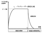
- FIG. 1 is a diagram showing an example of a microwave attenuation waveform.
- FIG. 2 is a schematic view showing the structure of the oxide semiconductor TFT used in the example.
- FIG. 3 is a schematic view showing an example of the configuration of an evaluation element used in the present invention.
- FIG. 4 is a schematic view showing an example of another configuration of the evaluation element used in the present invention.
- FIG. 5 is a schematic view showing an example of another configuration of the evaluation element used in the present invention.
- FIG. 6 is a schematic view showing an example of another configuration of the evaluation element used in the present invention.
- FIG. 7 is a schematic view of an evaluation substrate showing an example of the array configuration of evaluation elements used in the present invention.
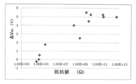
- FIG. 8 is a graph showing the relationship between ⁇ V th and electrical resistance in Example 1.
- FIG. 8 is a graph showing the relationship between ⁇ V th and electrical resistance in Example 1.
- FIG. 9 is a graph showing the relationship between ⁇ V th and the threshold shift amount of the repetitive sweep in the first embodiment.
- FIG. 10 is a graph showing the relationship between ⁇ V th in the first embodiment and the absolute value of the threshold voltage in the static characteristic.
- FIG. 11 is a graph showing the results of the IV characteristics in Example 2.
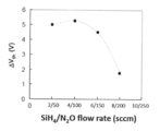
- FIG. 12 is a graph showing the relationship between the flow rate ratio of SiH 4 / N 2 O and ⁇ V th in Example 2.
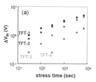
- the upper diagram of FIG. 13A is a graph showing the relationship between the stress application time and ⁇ V th in the second embodiment.
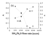
- the lower part of FIG. 13B is a graph showing the relationship between the flow rate ratio of SiH 4 / N 2 O and the A value and the n value constituting the slope B in Example 2.
- FIG. 13A is a graph showing the relationship between the stress application time and ⁇ V th in the second embodiment.
- the lower part of FIG. 13B is a graph showing the relationship between the flow rate ratio of SiH
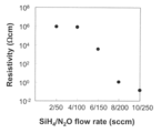
- FIG. 14 is a graph showing the relationship between the SiH 4 / N 2 O flow ratio and the sheet resistance in Example 2.
- FIG. 15 is a graph showing the relationship between V th and the slope B value in the second embodiment.
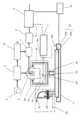
- FIG. 16 is a schematic explanatory view showing an example of an evaluation apparatus used in the present invention.
- the present inventors diligently studied to achieve the above object.
- an insulating film such as a gate insulating film, an oxide semiconductor thin film, a protective film formed on the surface of the oxide semiconductor thin film, and a first electrode such as a source electrode / drain electrode on a substrate
- a second The increase in the shift amount ⁇ Vh of the threshold voltage which occurs when a positive bias stress is applied to the TFT having an electrode is an interface state existing at the interface between the oxide semiconductor thin film and the protective film formed thereon
- the TFT has at least the above-mentioned configuration, and preferably refers to one having a configuration necessary for a TFT used in various display devices such as a liquid crystal display.
- the defects at the interface level cause band bending in the oxide semiconductor thin film, and as a result, the apparent resistance of the oxide semiconductor thin film, that is, the electronic state changes.
- the increase in ⁇ V th that occurs after the application of a positive bias has a good correlation with the electrical resistivity of the oxide semiconductor.
- sheet resistance (ohm * cm / (square)) or a specific resistance (ohm * cm) is mentioned as said electrical resistivity.
- the specific resistance is the sheet resistance multiplied by the film thickness.
- Threshold voltage V th of thin film transistor (2) When a positive bias is applied to the thin film transistor, the difference ⁇ V th between the threshold voltage before and after the application (3) The threshold when the threshold voltage of the thin film transistor is measured a plurality of times, and when it is measured for the first time.
- the electrical resistivity when measuring the electrical resistivity, it may be measured directly by a measuring means by a known contact method such as a four-terminal method or a four-probe method, It has also been found that nondestructive and noncontact and indirect measurements can be made based on noncontact methods such as the ⁇ -PCD method described later.
- the measurement may be performed using a laminate having a cross-sectional structure similar to that of the TFT.
- the shift of the threshold voltage which occurs upon application of a positive bias as described in (2) above is, as described above, an oxide semiconductor thin film and an etch stop layer for directly protecting the surface of the oxide semiconductor thin film , And “ESL”), so that the electrical resistivity of the oxide semiconductor thin film may be measured.
- the electrical resistivity may be measured using a TFT having the above-described configuration requirements.
- the TFT may have only the ESL on the surface of the oxide semiconductor thin film, and may further have a protective film for protecting the entire ESL on the ESL. When there is no ESL, a final protective film may be provided on the surface of the oxide semiconductor thin film.
- the structure of the TFT is not limited to the above example, and may have a configuration required for various liquid crystal display devices. Alternatively, it may have a cross-sectional structure similar to that of the TFT.
- the same series of manufacturing conditions until the oxide semiconductor thin film is formed are used.
- the manufacturing conditions for forming the oxide semiconductor thin film on the substrate are all the same including the type of the film and the heat treatment step.
- film forming conditions for forming an electrode such as a gate electrode, an insulating film such as a gate insulating film, or an oxide semiconductor thin film on a substrate are all including film types and heat treatment steps. Make the same condition.
- the interface defect is different from a defect in the oxide semiconductor thin film (hereinafter referred to as “in-film defect”). That is, as a result of the present inventors' investigation, as a cause of the luminance unevenness of the display device, it is caused by the shift of the threshold voltage when a positive bias is applied, and an interface defect affects. On the other hand, color jumps and display defects of display devices are caused by threshold voltage shifts due to light irradiation and negative bias (hereinafter sometimes referred to as "negative bias stress”), and defects in the film are affect. Therefore, both differ in the position of the defect in an oxide semiconductor thin film, and the defect location caused by it. Therefore, as described above, by setting the film forming conditions of the oxide semiconductor thin film under the same conditions and making the defects in the film the same state, the superiority or inferiority of the defects caused by the interface state can be evaluated.
- in-film defect a defect in the oxide semiconductor thin film
- an electrode may be provided on the surface of the oxide semiconductor thin film, and a current value or a voltage may be measured.
- a current value or a voltage may be measured.
- two pairs of ohmic electrodes are formed to measure the electrical resistivity.
- current can be supplied between a pair of electrodes formed on an oxide semiconductor thin film to measure a voltage between the pair of electrodes different from the electrodes.
- the electrical resistivity may be measured by the four probe method instead of the four probe method.
- a method of measuring the electrical resistivity by the four-probe method for example, a measuring method standardized by JIS H602 or the like may be applied.
- the electrical resistivity When the electrical resistivity is measured by the four-probe method, it can not be measured if the surface is covered with a protective film or the like. Therefore, the electrical resistivity can be measured by the four-point probe method if the protective film is removed only where the probe is in contact with the oxide semiconductor surface and the surface of the oxide semiconductor thin film can be brought into contact with the probe. .
- a measurement method such as a double ring electrode method may be mentioned.
- the measurement resistivity can be determined by bringing the measurement probe into direct contact with the surface of the oxide semiconductor thin film and supplying a current between the electrodes of the probe. Therefore, the dual ring electrode method is preferable because it is simpler and less expensive than the four-terminal method and the four-probe method which require electrode attachment.
- the noncontact method refers to measuring the electronic state without contacting the resistance measurement terminal with the oxide semiconductor thin film.
- the electronic state may measure the electrical resistivity nondestructively and indirectly in a noncontact manner by a noncontact method.
- the ⁇ -PCD method is exemplified as the noncontact method.
- the electrical resistivity can not be measured directly.
- the electrical resistivity can be evaluated indirectly.
- excitation light and a microwave are irradiated to the layered product which has a protective film on the surface of an oxide semiconductor thin film, and irradiation of the said excitation light
- the irradiation of the excitation light is stopped, and after the irradiation of the excitation light is stopped, from the oxide semiconductor thin film of the microwave
- the first step of measuring the temporal change of the reflectance of the reflected wave, and the parameter corresponding to the slow decay seen after the irradiation stop of the excitation light is calculated from the temporal change of the reflectance, and the oxidation
- a second step of evaluating the electronic state of the object semiconductor thin film is
- the present invention utilizes the microwave photoconductive attenuation method (hereinafter sometimes referred to as “ ⁇ -PCD method”) described in Patent Document 2.
- ⁇ -PCD method the microwave photoconductive attenuation method
- the present invention of the attenuation of microwaves obtained by the method of Patent Document 2, a slow microwave attenuation waveform seen in about 1 ⁇ s after stopping irradiation of excitation light, ie, the degree of microwave attenuation, It has a close correlation with the stress resistance after a positive bias stress application test for the oxide semiconductor thin film (hereinafter sometimes referred to as “positive bias stress application test”), and it is a non-contact type stress resistance. Therefore, the present invention is characterized in that it is extremely useful as an index that can be evaluated, predicted and measured accurately and easily.
- examples of the above-mentioned “parameter corresponding to the slow decay seen about 1 ⁇ s after stopping the irradiation of the excitation light” include the time until the microwave reflection intensity reaches 1 / e 2 of the maximum value; microwave The slope obtained by logarithmically converting the attenuation curve of the reflected wave intensity from 1 / e of the maximum value to 1 / e 2 of the maximum value, or the absolute value of the reciprocal of the slope; 1 ⁇ s after stopping the irradiation of excitation light The slope of the attenuation curve of the reflected wave intensity of about 2 ⁇ s, or the absolute value of the reciprocal of the slope; the reflected wave intensity of the microwave seen in about 1 ⁇ s after the irradiation light is stopped; the two attenuations of the attenuation of the reflected wave of the microwave In the case of the sum of functions, the longer one of the obtained logarithmically converted slopes, the absolute value of the reciprocal of the slopes, and
- B value represented by the relational expression of the power of Formula (1) of Example 2 described later as a slope is mentioned.
- the slope obtained by logarithmic conversion is, for example, ⁇ 1 described in the following formula (1), the following formula (2 Means ⁇ 2 described in 2. ).
- a slope obtained by logarithmically converting the attenuation curve of the microwave reflected wave intensity in a certain range, or the absolute value of the reciprocal of the slope is preferred.
- Particularly preferred parameters are slopes obtained by logarithmically converting the attenuation curve of the reflected wave intensity from 1 / e of the maximum value to 1 / e 2 of the maximum value, or the absolute value of the reciprocal of the slope, and around 1 ⁇ s to 2 ⁇ s The slope of the attenuation curve of the reflected wave intensity logarithmically converted, or the absolute value of the reciprocal of the slope.
- FIG. 1 is a diagram showing how excess carriers are generated and annihilated in the ⁇ -PCD method.
- the vertical axis in FIG. 1 corresponds to the reflectance of microwaves.
- the reflectance of the reflected wave from the oxide semiconductor thin film of microwaves once exhibits a maximum value, it rapidly attenuates at the same time as the irradiation of the excitation light is stopped. After that, an attenuation with a certain inclination is observed, but this inclination corresponds roughly to the “parameter corresponding to the slow attenuation observed after the termination of the irradiation of the excitation light” described above. This attenuation is affected by defects in the film and at the interface.
- the inclination for example, the inclination of the time in the above range and the reflectance that is the reflected wave strength
- the inclination of a value obtained by logarithmically converting the reflected wave strength with respect to the value obtained by logarithmically converting the time in the above range It can be mentioned.
- the B value in Formula (1) was used.
- this inclination includes the inclination when the reflectance attenuation after the termination of the excitation light irradiation is delayed.
- the sample used in the present invention is a laminate having an oxide semiconductor thin film and a protective film formed on the surface of the oxide semiconductor thin film on a substrate, and a laminate having the above-described various configurations can be used. .
- an amorphous oxide semiconductor thin film containing at least one or more elements selected from the group consisting of In, Ga, Zn, and Sn is preferably used. These elements may be contained singly or in combination of two or more. Specifically, for example, In oxide, In-Sn oxide, In-Zn oxide, In-Sn-Zn oxide, In-Ga oxide, Zn-Ga oxide, In-Ga-Zn oxide, Zn oxide etc. are mentioned.
- the thickness of the oxide semiconductor thin film is preferably, for example, about several tens of nm to 500 nm.
- the upper limit of the thickness is more preferably 200 nm or less, and still more preferably 100 nm or less.
- the lower limit of the thickness is more preferably 10 nm or more, and still more preferably 30 nm or more.
- a glass substrate for a liquid crystal display device having a thickness of about 0.7 mm and a size of several tens cm 2 to several m 2 which is called the first generation to the tenth generation can be used.
- the protective film (hereinafter sometimes referred to as “passivation insulating film”) is a protective film for directly protecting the surface of the oxide semiconductor thin film (hereinafter sometimes referred to as “etch stop layer” or “ESL”) And a protective film for further protecting the surface of the protective film (hereinafter sometimes referred to as “final protective film”).
- Excitation light and microwaves are applied to such a stack.
- the carrier concentration of the oxide semiconductor thin film can be determined by analyzing the change in excess carrier density, and the electronic state, and hence the electrical resistivity, that is, the sheet resistance or specific resistance can be evaluated as follows: Seems to be based on the following reasons.
- the microwaves irradiated to the stack are reflected by plasma vibration by carriers present in the oxide semiconductor thin film. This reflectance depends on the carrier density in the oxide semiconductor thin film. However, in the oxide semiconductor thin film in the steady state, there is no number of carriers at a level at which microwave reflection can be practically observed. However, when the excitation light is irradiated, excess carriers are generated in the film, and the plasma vibration of the excess carriers increases the reflectance of the microwave. On the other hand, the irradiation stop of excitation light reduces the reflectance of microwaves as the number of excess carriers decreases.
- carriers in a silicon semiconductor or the like are generated due to the shallow donor level existing in the lower part of the conduction band in the energy band.
- the energy level in this case is about several tens of meV below the conduction band, and is almost activated around room temperature.
- carriers in the oxide semiconductor thin film in the steady state are also known to be caused by the shallow donor level existing in the lower part of the conduction band in the energy band, but in oxide semiconductor, the level is It is about 0.1 to 0.2 eV and relatively deep. For this reason, excess carriers generated by irradiation of excitation light may be once captured and re-emitted at the donor level, as well as when the excited holes and electrons recombine.
- the rate of capture and re-emission is dependent on the amount of shallow donor levels present in the lower energy band in the energy band. Therefore, by tracing the annihilation process observed after the termination of the excitation light, it is possible to analyze the influence of the donor level on the excess carriers generated by the irradiation of the excitation light.
- the specific resistance of the oxide semiconductor thin film is expressed by the product of charge, free electrons, and mobility, and the mobility of the oxide semiconductor thin film is the same as the composition of the metal element that forms the oxide semiconductor thin film. If it does not change much.
- the mobility of a-IGZO is about 10 cm 2 / VS. Therefore, the change in the reflectance of microwaves observed in the ⁇ -PCD method, that is, the change in the excess carrier density, is roughly correlated with the carrier concentration and the electrical resistivity.
- amorphous semiconductor materials such as oxide semiconductors have continuous levels between the conduction band and the donor level such as amorphous silicon and IGZO.
- the annihilation process of carriers observed in the ⁇ -PCD method can be understood as superposition of individual carrier transition behavior between each level.
- the decay process is observed over a somewhat long time range as compared to the transition between one level.
- the time dependency at that time has a power-to-power relationship with respect to time.
- determining the carrier density of the oxide semiconductor thin film by calculating the parameter corresponding to the slow decay which is generally found in the time range over the range of 0.1 to 10 ⁇ s after the first step described above. Can. Based on the result, the electrical resistivity such as sheet resistance and resistivity can be evaluated.
- a method of evaluating a defect caused by the interface state between the oxide semiconductor thin film and the protective film by the above evaluation method is applied to any of the steps of the semiconductor manufacturing process. It also includes methods of quality control.
- the electronic state of the oxide semiconductor thin film that is, the result of evaluating the electrical resistivity is fed back, and the manufacturing conditions
- the quality of the oxide semiconductor can be properly controlled because the film quality can be managed by adjusting the
- the evaluation method of the present invention when the protective film is formed on the obtained oxide semiconductor thin film; or when heat treatment (hereinafter sometimes referred to as “post annealing”) is performed after that, the evaluation method of the present invention is used. It is preferable to apply.
- the stress resistance of the oxide semiconductor thin film can be easily evaluated in a short time at low cost in the material development stage of the oxide semiconductor thin film.
- the electrical characteristics of the oxide semiconductor thin film can be evaluated inline in a short time in a manufacturing line of a liquid crystal display device or the like.
- productivity can be improved, for example, the yield can be improved, and quality control of the oxide semiconductor can be appropriately performed.
- the evaluation element has an oxide semiconductor thin film on a substrate and a protective film on the oxide semiconductor thin film.
- the following evaluation element (a) or (b) may be mentioned.
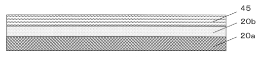
- the oxide semiconductor thin film is directly formed on the surface of the formed evaluation element (b) the insulating film such as the gate insulating film, and the etch stop layer 45 described in FIG. 5 or FIG.
- a gate insulating film is described as a typical example as the insulating film, but it may be formed between the substrate and the oxide semiconductor thin film, and is not limited to the gate insulating film.
- the oxide semiconductor thin film be formed directly on the surface of the substrate or the gate insulating film as described in (a) or (b). That is, no metal electrode such as a gate electrode exists immediately below the oxide semiconductor thin film. If the gate electrode or the like exists immediately below the oxide semiconductor thin film, the number of free carriers of the gate electrode is 10 18 cm -3 or more, so the influence of the gate electrode is dominant on the reflectance of the microwave. It is because
- FIGS. 3 to 6 An example of the configuration of the evaluation element used in the present invention is shown in FIGS. 3 to 6, no metal electrode is provided immediately below the oxide semiconductor thin film.
- a gate insulating film 43, a patterned oxide semiconductor thin film 20b, and an etch stop layer 45 which is a patterned protective film are formed in this order on a substrate 20a such as a glass substrate.
- a gate insulating film 43, a patterned oxide semiconductor thin film 20b, a patterned etch stop layer 45, and a final protective film 47 are formed in this order on a substrate 20a.
- the gate insulating film 43, the oxide semiconductor thin film 20b, and the etch stop layer 45 are formed in this order on the substrate 20a.
- FIG. 6 shows an oxide semiconductor thin film 20b and an etch stop layer 45 formed in this order on a substrate 20a.
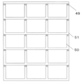
- an evaluation substrate in which a plurality of the above-described evaluation elements are disposed on the substrate.
- FIG. 7 is a schematic view showing an example of the configuration of the evaluation substrate.
- a display 50 and a plurality of evaluation elements 49 are regularly arranged and installed on a mother glass 51 such as a glass substrate used in a mass production line.
- a mother glass 51 such as a glass substrate used in a mass production line.
- FIG. 16 is a schematic view showing an example of the configuration of an apparatus used for the method of evaluating an oxide semiconductor thin film.
- the evaluation apparatus shown in FIG. 16 irradiates excitation light to the measurement site of the sample 20 in which the oxide semiconductor thin film 20b is formed on the substrate 20a to generate electron-hole pairs in the oxide semiconductor thin film.
- the detection means 7 is provided with means for evaluating the electrical resistivity of the sample 20 based on the detection data of the reflection microwave intensity detection means, and the change in the reflectivity and the electrical resistivity indirectly with the same device by this configuration. Can be measured and evaluated.
- the excitation light irradiation means 1 has a light source for outputting excitation light to be irradiated to the sample 20, and generates electron-hole pairs in the oxide semiconductor thin film by irradiation of the excitation light. It is preferable to have a light source which outputs energy higher than the band cap of the oxide semiconductor thin film. It is preferable because carriers can be efficiently generated by outputting energy higher than the band gap of the oxide semiconductor thin film and measurement can be performed with high sensitivity.
- an ultraviolet laser may be used as a light source.
- a pulse-like ultraviolet light having a wavelength of 349 nm, a power of 1 ⁇ J / pulse, a pulse width of about 15 ns, and a beam diameter of about 1.5 mm, for example, a semiconductor laser such as a pulsed laser that emits YF laser third harmonic waves as excitation light. Etc.
- the excitation light irradiation means 1 outputs pulse light which is excitation light, using the input of the timing signal transmitted (broken line in the figure) from the evaluation means 9 as a trigger.
- the timing signal is also transmitted to the signal processor 8 at the same time.
- the output of the excitation light output from the excitation light irradiation means 1 can be adjusted by the output adjustment power monitor 16a and the output adjustment means 16b.
- the excitation light output from the excitation light irradiation means 1 is reflected by an optical path changing means (hereinafter may be referred to as a "mirror") 12 such as a mirror, and a focusing means such as a focusing lens (not shown)
- a mirror such as a mirror
- a focusing means such as a focusing lens
- the measurement site of a diameter of about 5-10 ⁇ m of the sample 20 is irradiated through 6d).
- the mirror 12 and the condenser lens condense the excitation light output from the excitation light irradiation means 1 and guide it to the measurement site of the sample 20.
- excitation carriers are generated in a minute excitation light irradiation area 21 which is a measurement site in the sample 20.
- the microwave irradiation means 3 is a means for outputting a microwave to be irradiated to the measurement site of the sample 20.
- the microwave irradiation means 3 may be, for example, a microwave oscillator such as a Gunn diode having a frequency of 26 GHz.
- the directional coupler 4 branches the microwave output from the microwave irradiation unit 3 into two.
- One output wave after branching (hereinafter referred to as the first microwave Op1) is transmitted to the magic T (5) side, and the other output wave (hereinafter referred to as the second microwave Op2) is the phase adjuster 4a, the reflection micro
- the signal is transmitted to the LO input terminal of the wave intensity detection means 7.
- a 10 dB coupler or the like is employed as this directional coupler 4.
- the magic T (5) branches the first microwave Op1 into two, and the difference signal Rt1 of each of the reflected waves of the two first branched microwaves with respect to the sample 20 (hereinafter referred to as "reflected wave difference signal” And the sum signal.
- first main microwave Op11 One of the microwaves Op1 bifurcated by the magic T (5) (hereinafter sometimes referred to as "first main microwave Op11") is provided by the first waveguide 6a connected to the magic T (5) The light is led to the measurement site including the excitation portion of the sample 20 and emitted from the opening 6 d at the tip. Thereby, the measurement region of the sample 20 is irradiated with the first main microwave Op11. Furthermore, in addition to the function as an antenna (hereinafter sometimes referred to as “waveguide antenna”) that radiates the first main microwave Op11, the first waveguide 6a also emits the first main The reflected wave of the wave Op11 is captured by the opening 6d at the tip, and it also functions to guide it back to the magic T (5).
- microwaveguide antenna an antenna
- first sub microwave Op12 the other of the first microwave Op1 branched into two by the magic T (5) (hereinafter, referred to as "first sub microwave Op12") is a second waveguide 6b connected to the magic T (5)
- the light is guided to the vicinity of the measurement site of the sample 20a, but not to the excitation part by the excitation light and emitted from the opening 6e at the tip thereof.
- the first sub-microwave Op12 is irradiated in the vicinity of the measurement region of the sample 20a.
- the second waveguide 6b has an opening at the tip of the reflected wave of the first sub-microwave Op12 irradiated near the measurement site. It also captures the part 6e and plays back the magic T (5).
- the path length in which the first waveguide 6a guides the microwaves is equal to the path length in which the second waveguide 6b guides the microwaves.
- a difference signal that is, a reflected wave difference signal Rt1 is output by its magic T (5) and transmitted to the RF input end of the reflected microwave intensity detection means 7.
- the reflected microwave intensity detection means 7 outputs the detection signal Sg1 by mixing the second microwave Op2 and the reflected wave difference signal Rt1.
- the detection signal Sg1 is a signal representing an example of the intensity of the reflected wave difference signal Rt1, for example, the intensity of the reflected wave of the first microwave Op1 emitted to the sample 20, and is taken into the signal processing device 8.
- the intensity of the reflected wave difference signal Rt1 is changed by the irradiation of the excitation light to the sample 20 held at a predetermined position by the substrate holding unit.
- the reflected microwave intensity detection means 7 detects the intensity of the reflected wave difference signal Rt 1, and as the reflected microwave intensity detection means 7, a mixer or a microwave is inputted and the intensity is determined according to the intensity.
- a microwave detector (hereinafter sometimes referred to as a "detector") that outputs an electrical signal, that is, a current or a voltage, may be provided.
- the intensity of the reflected wave difference signal Rt1 detected by the reflected microwave intensity detection means 7 is changed by the irradiation of the excitation light to the measurement site of the sample 20. Specifically, the intensity of the reflected wave difference signal Rt1 is attenuated after being temporarily increased by the irradiation of the excitation light.
- the peak value of the intensity of the reflected wave difference signal Rt1 decreases as the number of impurities, defects, and the like increase at the measurement site, and the attenuation time, that is, the carrier life also decreases.
- the parameter corresponding to the slow decay seen after the excitation light irradiation stops after the peak value is generated is the electronic state of the sample 20, ie, the electrical resistance It becomes an index to evaluate the rate.
- the signal processing device 8 is a device that detects the peak value Sp of the change in intensity of the reflected wave difference signal Rt1 detected by the reflected microwave intensity detection means 7 and transmits the detection result to the evaluation means 9. More specifically, the signal processing device 8 monitors the change of the reflected wave difference signal Rt1 for a predetermined time using the input of the timing signal from the evaluation means 9 as a trigger, and the maximum value of the level of the reflected wave difference signal Rt1 obtained during that time Is detected as the peak value Sp of the change in the intensity of the reflected wave difference signal Rt1.
- the signal processing device 8 includes a delay circuit that performs delay processing on the reflected wave difference signal Rt1, sequentially detects the signal strength of the signal after delay processing at a predetermined sampling frequency, and changes in the detected value.
- the peak value Sp of the change of the intensity of the reflected wave difference signal Rt1 is detected.
- a computer provided with a CPU, a storage unit, an interface of input / output signals and the like can be used, and the CPU executes various processes by executing a predetermined program.
- the evaluation means 9 outputs a timing signal representing the output timing of the excitation light to the excitation light irradiation means 1 and the signal processing device 8 and also the peak value of the reflected wave difference signal Rt1 detected by the signal processing device 8 Sp is taken in and recorded in the storage unit included in the evaluation unit 9.
- the recorded reflected wave difference signal Rt1 (detection data) is used to evaluate the electronic state of the sample 20, that is, the electrical resistivity.
- stage controller 10 controls the positioning of the measurement site on the sample 20 by controlling the XY stage 11 in accordance with the command from the evaluation means 9.
- a sample table (not shown) is provided on the upper side of the XY stage 11.
- the sample stand is a plate-like conductor member made of metal such as aluminum, stainless steel or iron or other conductor.
- a substrate holder (not shown) is provided on the upper side, and the sample 20 is placed on the substrate holder.
- the sample stage is disposed on the side opposite to the side irradiated with the first microwaves Op11 and Op12 with respect to the sample 20, that is, on the lower side of the sample 20.
- the substrate holder is a solid dielectric fixed on the upper side of the sample stage.
- the substrate holder is a solid dielectric inserted between the substrate and the sample table, and the material is, for example, a dielectric having a relatively large refractive index, such as glass or ceramic.
- substrate holding part a medium becomes short by this, and it can employ
- the structure for evaluating the electronic state of the oxide semiconductor thin film of this invention while a photoexcitation carrier is produced
- the photoexcited carriers move in the electric field of the microwave irradiated from the irradiation means 3 and the movement state is influenced by the presence of impurities, defects and the like in the semiconductor.
- the reflected microwave intensity detection means 7 detects the intensity of the reflected microwave from the sample, and the change in the excess carrier concentration is analyzed as already described in the evaluation means 9 to obtain the carrier of the oxide semiconductor thin film.
- the concentration can be determined, and the electrical resistivity can be evaluated indirectly from the change of the electronic state.
- the evaluation device of the present invention with an electrical resistance measurement means, it is possible to provide a device that evaluates not only the electrical resistivity but also the electrical characteristics of the oxide semiconductor thin film inline in a short time. it can.
- the electrical resistivity is evaluated based on so-called slow decay.
- slow decay is also affected by defects in the film of the oxide semiconductor thin film, and it is measured and evaluated based on the above-mentioned ⁇ -PCD method by the degree of defects in the film.
- the electrical resistivity also changes.
- the electrical resistivity of the oxide semiconductor thin film may differ due to contamination or impurities even in the same plane, and the value varies depending on the measurement location. Therefore, in order to perform more appropriate quality control of the oxide semiconductor thin film, it is important that the measurement site by the ⁇ -PCD method and the measurement site by the electrical resistivity measurement means be substantially the same.
- an electric resistance measurement means is provided in the above-mentioned evaluation apparatus, it is possible to measure the substantially same place simply and accurately simply by moving the XY stage appropriately. Therefore, if the above-mentioned evaluation device provided with the electrical resistance measurement means is used for a manufacturing line such as a liquid crystal display device, productivity can be greatly improved, and more appropriate quality control of the oxide semiconductor thin film can be performed.
- FIG. 16 shows an apparatus provided with the electrical resistance measuring means 30 in the apparatus for measuring and evaluating the change in reflectance and the electrical resistivity based on the ⁇ -PCD method described above.
- the electrical resistance measuring means 30 may not necessarily be installed. Although the specific installation location is not limited, by moving the XY stage 11 as described above, the electrical resistivity is measured by the electrical resistance measurement means 30 at substantially the same location as the microwave photoconductivity measurement location of the oxide semiconductor thin film It is desirable to install as you can.
- the electrical resistance measuring means 30 preferably comprises an electrical resistivity measuring head 31 and lifting and lowering means 32 of the electrical resistivity measuring head 31.
- the electrical resistivity measurement means 30 can measure the electrical resistivity of the sample 20.
- the electrical resistivity measuring head 31 is a means for measuring the electrical resistivity by a contact method.
- the electrical resistivity measurement head 31 is provided with a resistance measurement terminal corresponding to the above-described resistance measurement means, and as the resistance measurement terminal, a measurement probe such as a double ring electrode or four needle-like electrodes on a straight line The head etc. which arranged the are illustrated.
- the electrical resistivity of the oxide semiconductor thin film can be measured by resistance measurement using a double ring electrode in accordance with JIS K6911, or resistance measurement by a four-probe method in accordance with JIS K7194.
- the elevating means 32 of the electrical resistivity measuring head 31 is an elevating mechanism which lowers the electrical resistivity measuring head to a desired position when measuring the electrical resistivity of the sample 20.
- Various well-known electric resistivity measuring devices can be used as a means to measure an electric resistivity.
- an electrical resistance measuring device such as a JANDEL probe head can be similarly evaluated.
- the electrical resistivity can be changed by changing the flow ratio of silane in the mixed gas at the time of forming the protective film, as shown in the examples described later. Therefore, it is also possible to obtain a desired electrical resistivity by optimizing the protective film formation conditions. At that time, it is important that the electrical resistivity of the oxide semiconductor thin film changes when the properties of the oxide semiconductor itself change.
- the film was formed under the same condition and subjected to the same heat treatment as a precondition. It is necessary to prepare a plurality of oxide semiconductor thin films having substantially the same state. This makes it clear that the actual change in electrical resistivity is due to the formation of the protective film, so that it is possible to accurately determine the superiority and inferiority.
- the evaluation method of the present invention stress resistance of the oxide semiconductor thin film can be easily evaluated in a short time and at low cost in the process of optimization of the TFT manufacturing process. Furthermore, if the evaluation method of the present invention is used, the electrical characteristics of the oxide semiconductor thin film can be evaluated inline in a short time in a manufacturing line of a liquid crystal display device or the like. In addition, according to the ⁇ -PCD method, evaluation can be performed in a noncontact manner, so that productivity can be improved, such as improvement in yield, and quality control of the oxide semiconductor can be appropriately performed.
- Example 1 characteristics due to stress after application of a positive bias were evaluated by directly measuring the electrical resistivity of the oxide semiconductor thin film.
- a laminate sample for electrical resistivity measurement was produced as in the following (1), and a TFT for TFT characteristic measurement was produced as in the following (2).
- the sample of the above (1) is a laminate having the same cross-sectional structure as the TFT of the following (2) in that the gate insulating film, the oxide semiconductor thin film, and the protective film are formed on the substrate.
- a SiO 2 insulating film corresponding to a gate insulating film is formed to a film thickness of 200 nm on a glass substrate (EAGLE 2000 manufactured by Corning) having a diameter of 100 mm and a thickness of 0.7 mm.
- the film was formed.
- an oxide semiconductor thin film was formed by sputtering.
- the apparatus used for sputtering is “CS-200” manufactured by ULVAC, Inc.
- Pre-annealing was performed to improve the film quality. Pre-annealing was performed at 350 ° C. for 60 minutes under 100% oxygen atmosphere and atmospheric pressure.
- SiO 2 was formed to have a film thickness of 100 nm by plasma CVD.
- the gas used for film formation is a mixed gas of SiH 4 / N 2 O, and the flow rate (unit: sccm / sccm) is in the range of 2/50, 4/100, 6/150, 8/200, 10/250. In various ways.
- the film forming temperature was 230.degree.
- an ohmic electrode was produced. Specifically, pure Mo was used, and film formation was performed to a film thickness of 100 nm by DC sputtering, and then patterning was performed.
- a SiO 2 film having a thickness of 200 nm and a SiN film having a film thickness of 200 nm: a total film thickness of 400 nm were used as a final protective film for blocking the external atmosphere.
- the formation of SiO 2 and SiN was performed using plasma CVD method using Samco “PD-220NL”.
- a mixed gas of N 2 O and SiH 4 was used to form the SiO 2 film, and a mixed gas of SiH 4 , N 2 , and NH 3 was used to form the SiN film.
- the film forming power was 100 W, and the film forming temperature was 150 ° C.
- a contact hole for connection for measuring the electrical resistance was formed in the protective film by photolithography and dry etching to obtain a sample for electrical resistivity measurement.
- the sheet resistance of the sample was measured by applying a voltage between the electrodes. Specifically, current-voltage characteristics were measured using a National Instruments “4156C” semiconductor parameter analyzer.
- a Mo thin film as a gate electrode was formed to 100 nm on a glass substrate (EAGLE 2000 manufactured by Corning) having a diameter of 100 mm and a thickness of 0.7 mm.
- the gate electrode was formed by DC sputtering using a pure Mo sputtering target.
- the sputtering conditions are: substrate temperature: room temperature, gas pressure: 2 mTorr.
- a 200 nm thick gate insulating film SiO 2 and a 40 nm thick oxide semiconductor thin film are sequentially formed and patterned on the gate electrode thus obtained in the same manner as (1), and pre-annealing is performed. After that, an etch stop layer and a final protective film were formed in the same manner as in (1) above.
- Mo thin film was formed as a source electrode * drain electrode.
- the film formation method and patterning method of the pure Mo film are the same as in the case of the gate electrode described above, and the channel length of the TFT is 10 ⁇ m, and the channel width is 200 ⁇ m.
- a protective film for protecting the oxide semiconductor thin film was formed in the same manner as in (1) above, and a contact hole was formed to obtain a sample for TFT measurement.
- TFT characteristics of each TFT thus obtained were examined as follows. Specifically, (I) transistor characteristics: IV characteristics, specifically (i) absolute value of threshold voltage, and (ii) repeated initial characteristics were examined. In addition, the change ⁇ V th of the threshold voltage V th when the (II) positive bias stress application test was performed was investigated.
- the threshold voltage is roughly the value of the gate voltage when the transistor is turned off, that is, when the drain current is transitioned from a low state to an on state, ie, a high drain current.
- the drain current is a voltage when a near 1nA during the on current and the off current is defined as the threshold V th voltage, measure the amount of change [Delta] V th of the threshold voltage before and after stress application did. The smaller the ⁇ V th , the better the stress tolerance.
- FIG. 8 shows the relationship between the vertical axis: ⁇ V th (V) in the positive bias stress application test and the horizontal axis: the electrical resistance ( ⁇ ) between the electrodes. From the above figure, it can be seen that the behavior of ⁇ V th and the electrical resistivity almost match.
- FIG. 9 shows the relationship between the vertical axis: the threshold shift amount (V) of the repeated sweep and the horizontal axis: ⁇ V th (V) measured by the method of (II) above.
- FIG. 10 shows the relationship between the vertical axis: the absolute value (V) of the threshold voltage in the static characteristic and the horizontal axis: ⁇ V th (V). From these figures, it can be seen that both ⁇ V th and the absolute value of the threshold voltage in the static characteristics and the threshold shift amount of the repetitive sweep have a good correlation.
- Example 2 characteristics due to stress after application of a positive bias were evaluated by measuring the electrical resistivity of the oxide semiconductor thin film indirectly by the ⁇ -PCD method.
- Example 1 various characteristics were evaluated using the sample produced in Example 1 above. The results are shown in Table 1.
- the ESL is obtained by changing the flow rate (sccm / sccm) of SiH 4 / N 2 O in the range of 2/50, 4/100, 6/150, 8/200, 10/250.
- ⁇ V th after 2 hours is as follows.
- V TFT-4 1.75 V TFT-5: -0.25V
- the “parameter corresponding to the slow decay seen after irradiation of the excitation light” in the ⁇ -PCD method was measured.
- the ⁇ -PCD method is performed under the following conditions: It implemented and measured the time change of reflectance.
- the “parameter corresponding to the slow attenuation” defined in the present invention “tilt” is used in this embodiment.
- the “B” value was calculated when the relationship between the reflectance and the measurement time was expressed by the following equation (1).
- FIG. 11 shows the IV characteristics of each of the TFTs 1-5. It can be seen from FIG. 11 that the operation of the TFT changes with the flow ratio of SiH 4 / N 2 O.
- FIG. 12 is a graph showing the relationship between the flow rate ratio of SiH 4 / N 2 O and ⁇ V th . From FIG. 12, it can be seen that ⁇ V th in the positive bias stress application test becomes smaller as the flow rate of SiH 4 / N 2 O is increased.
- FIG. 13A is a double logarithm graph plotting values of ⁇ V th at each stress application time in each TFT. From FIG. 13A, it was found that they exhibited good linearity and had a relationship described by power-law with respect to stress application time.
- the trap level of the above interface is formed by separating from the interface bonding and diffusing away from the interface (Paper name: S. Nakano, N. Saito, K. Miura, T. Sakano, T. Ueda, K. Sugi, H. Yamaguchi, I. Amemiya, M. Hiramatsu, A. Ishida, K. Kanomaru, and M. Sawada, IDW '11, 1271 (2011)). Therefore, the results in the above figure show that the interface state between ESL and IGZO is reduced by increasing the flow ratio of SiH 4 / N 2 O.
- FIG. 14 shows the relationship between the sheet resistance and the flow rate of SiH 4 / N 2 O. From the above figure, it can be seen that the sheet resistance decreases as the flow rate of SiH 4 increases. It can be seen that ⁇ V th and the sheet resistance are correlated, considering the result of FIG. 15 described above. Although not shown, it is known from the result of capacitance-voltage (CV) measurement performed using a MOS diode that the donor density is about 1 ⁇ 10 18 cm ⁇ 3 in each sample. The specific resistance of the a-IGZO film under the same conditions is estimated to be 2.7 ⁇ cm from the Hall effect measurement result of thick IGZO film, and the sheet resistance is larger than the value expected from the result. Therefore, it was strongly suggested that the rapid increase of the sheet resistance is due to band bending due to the increase of the interface state.
- CV capacitance-voltage
- the threshold voltage in the repetitive sweep characteristic and the static characteristic has a good correlation with ⁇ V th in the positive bias stress application test.
- This result strongly suggests that the threshold voltage in the repetitive sweep characteristic and the static characteristic described above is also caused by the interface state at the interface between ESL and IGZO, as in the above ⁇ V th .
- the cause of the increase in the interface state is unknown in detail, but considering that the film formation time in ESL film formation is largely different, it is presumed that plasma damage during ESL film formation is the cause of interface state formation. Be done.
- FIG. 15 shows the relationship between ⁇ V th (V) obtained by the method of Example 1 and the B value obtained by the ⁇ -PCD method. From FIG. 15, it can be seen that ⁇ V th and the B value show a U-shaped curve and are correlated. In particular if the [Delta] V th is less than the apex [Delta] V th ⁇ 3.5 V of the U-shaped curve, as [Delta] V th decreases, the B value can be increased were found to be absolute values. Further, it can be understood from the above figure that the B value which is an absolute value is influenced by the ratio of the amount of silane at the time of forming the protective film.
- the B value be useful as an indicator of the sheet resistance and [Delta] V th, consequently, the sheet resistance of oxide semiconductor thin film by using the above B value It can be seen that can be evaluated.
- excitation light irradiation means 3 microwave irradiation means 4 directional coupler 4a phase adjuster 5 magic T 6a first waveguide 6b second waveguide 6c minute aperture 6d, 6e aperture 7 reflection microwave intensity detecting means 8 signal processing device 9 evaluation means 10 stage controller 11 XY stage 12 optical path changing means 16a output Adjustment power monitor 16b Power adjustment means 20 Sample 20a Substrate 20b Oxide semiconductor thin film 21 Excitation light irradiation area 30 Electric resistivity measurement means 31 Electric resistivity measurement head 32 Elevation means 33 Measured value transmission line 42 Gate electrode 43 Gate insulating film 45 Etch stop layer 46a Source electrode 46b Drain electrode 47 Final protective film 48 Contact hole 49 Evaluation element 50 Display 51 Mother glass
Landscapes
- Engineering & Computer Science (AREA)
- Manufacturing & Machinery (AREA)
- Microelectronics & Electronic Packaging (AREA)
- Physics & Mathematics (AREA)
- Computer Hardware Design (AREA)
- Power Engineering (AREA)
- General Physics & Mathematics (AREA)
- Condensed Matter Physics & Semiconductors (AREA)
- Health & Medical Sciences (AREA)
- Electromagnetism (AREA)
- Toxicology (AREA)
- Thin Film Transistor (AREA)
- Testing Or Measuring Of Semiconductors Or The Like (AREA)
- Electrodes Of Semiconductors (AREA)
- Analysing Materials By The Use Of Radiation (AREA)
Priority Applications (4)
| Application Number | Priority Date | Filing Date | Title |
|---|---|---|---|
| US15/316,801 US10203367B2 (en) | 2014-07-01 | 2015-06-22 | Quality evaluation method for laminate having protective layer on surface of oxide semiconductor thin film and quality control method for oxide semiconductor thin film |
| EP15814922.9A EP3166133A4 (en) | 2014-07-01 | 2015-06-22 | Quality evaluation method for laminate having protective layer on surface of oxide semiconductor thin film and quality control method for oxide semiconductor thin film |
| CN201580031246.8A CN106463433B (zh) | 2014-07-01 | 2015-06-22 | 氧化物半导体薄膜层叠体的品质评价方法及品质管理方法 |
| KR1020167036722A KR101923798B1 (ko) | 2014-07-01 | 2015-06-22 | 산화물 반도체 박막의 표면에 보호막을 갖는 적층체의 품질 평가 방법 및 산화물 반도체 박막의 품질 관리 방법 |
Applications Claiming Priority (2)
| Application Number | Priority Date | Filing Date | Title |
|---|---|---|---|
| JP2014-136349 | 2014-07-01 | ||
| JP2014136349A JP6283273B2 (ja) | 2014-07-01 | 2014-07-01 | 薄膜トランジスタ評価用の積層構造体の評価方法 |
Publications (1)
| Publication Number | Publication Date |
|---|---|
| WO2016002554A1 true WO2016002554A1 (ja) | 2016-01-07 |
Family
ID=55019098
Family Applications (1)
| Application Number | Title | Priority Date | Filing Date |
|---|---|---|---|
| PCT/JP2015/067848 Ceased WO2016002554A1 (ja) | 2014-07-01 | 2015-06-22 | 酸化物半導体薄膜の表面に保護膜を有する積層体の品質評価方法、及び酸化物半導体薄膜の品質管理方法 |
Country Status (7)
| Country | Link |
|---|---|
| US (1) | US10203367B2 (enExample) |
| EP (1) | EP3166133A4 (enExample) |
| JP (1) | JP6283273B2 (enExample) |
| KR (1) | KR101923798B1 (enExample) |
| CN (1) | CN106463433B (enExample) |
| TW (1) | TWI652749B (enExample) |
| WO (1) | WO2016002554A1 (enExample) |
Cited By (1)
| Publication number | Priority date | Publication date | Assignee | Title |
|---|---|---|---|---|
| CN111855704A (zh) * | 2020-07-28 | 2020-10-30 | 哈尔滨工业大学 | 双极晶体管电离损伤敏感部位的检测方法 |
Families Citing this family (8)
| Publication number | Priority date | Publication date | Assignee | Title |
|---|---|---|---|---|
| JP5993496B2 (ja) * | 2014-07-16 | 2016-09-14 | 株式会社神戸製鋼所 | 酸化物半導体薄膜、及び前記酸化物半導体薄膜の表面に保護膜を有する積層体の品質評価方法、及び酸化物半導体薄膜の品質管理方法 |
| US10475711B2 (en) | 2016-04-27 | 2019-11-12 | Kobe Steel, Ltd. | Method for evaluating quality of oxide semiconductor thin film, method for managing quality of oxide semiconductor thin film, and device for manufacturing semiconductor using said method for managing quality |
| KR102161466B1 (ko) * | 2019-11-21 | 2020-10-05 | 주식회사 아바코 | 산화물 반도체 박막 검사장치 |
| US12094787B2 (en) | 2021-08-03 | 2024-09-17 | Applied Materials, Inc. | Characterizing defects in semiconductor layers |
| JP7249395B1 (ja) * | 2021-11-10 | 2023-03-30 | 株式会社Sumco | 半導体試料の評価方法、半導体試料の評価装置および半導体ウェーハの製造方法 |
| KR102732045B1 (ko) * | 2022-01-28 | 2024-11-20 | 연세대학교 산학협력단 | 공정 모니터링 방법 및 장치 |
| JP2024048269A (ja) * | 2022-09-27 | 2024-04-08 | 株式会社ジャパンディスプレイ | 半導体装置の製造方法 |
| JP2024172734A (ja) | 2023-06-01 | 2024-12-12 | 株式会社ディスコ | ゲッタリング層検出装置 |
Citations (6)
| Publication number | Priority date | Publication date | Assignee | Title |
|---|---|---|---|---|
| JP2002098634A (ja) * | 2000-03-27 | 2002-04-05 | Tochigi Nikon Corp | 半導体の電気特性評価装置および電気特性評価方法 |
| JP2011054863A (ja) * | 2009-09-04 | 2011-03-17 | Institute Of Physical & Chemical Research | 移動度測定装置及びその方法、並びに、抵抗率測定装置及びその方法 |
| JP2011249788A (ja) * | 2010-04-28 | 2011-12-08 | Semiconductor Energy Lab Co Ltd | 半導体装置の作製方法 |
| JP2012033857A (ja) * | 2010-06-30 | 2012-02-16 | Kobe Steel Ltd | 酸化物半導体薄膜の評価方法、及び酸化物半導体薄膜の品質管理方法 |
| JP2013168575A (ja) * | 2012-02-16 | 2013-08-29 | Univ Of Tokyo | 伸縮性回路基板 |
| JP2013254948A (ja) * | 2012-05-09 | 2013-12-19 | Kobe Steel Ltd | 薄膜トランジスタおよび表示装置 |
Family Cites Families (14)
| Publication number | Priority date | Publication date | Assignee | Title |
|---|---|---|---|---|
| JP5213458B2 (ja) | 2008-01-08 | 2013-06-19 | キヤノン株式会社 | アモルファス酸化物及び電界効果型トランジスタ |
| JP2010040552A (ja) * | 2008-07-31 | 2010-02-18 | Idemitsu Kosan Co Ltd | 薄膜トランジスタ及びその製造方法 |
| JP5564331B2 (ja) * | 2009-05-29 | 2014-07-30 | 株式会社半導体エネルギー研究所 | 半導体装置の作製方法 |
| JP5507133B2 (ja) * | 2009-07-03 | 2014-05-28 | 富士フイルム株式会社 | ボトムゲート構造の薄膜トランジスタの製造方法 |
| KR20120090972A (ko) * | 2009-09-24 | 2012-08-17 | 가부시키가이샤 한도오따이 에네루기 켄큐쇼 | 반도체 장치 및 그 제조 방법 |
| DE112010003968B4 (de) | 2009-10-06 | 2016-12-29 | Kabushiki Kaisha Kobe Seiko Sho (Kobe Steel, Ltd.) | Einrichtung und Verfahren zum Messen einer Halbleiterladungsträgerlebensdauer |
| US10996258B2 (en) * | 2009-11-30 | 2021-05-04 | Ignis Innovation Inc. | Defect detection and correction of pixel circuits for AMOLED displays |
| CN102313849B (zh) * | 2010-06-30 | 2014-08-06 | 株式会社神户制钢所 | 氧化物半导体薄膜的评价方法及氧化物半导体薄膜的质量管理方法 |
| JP5350345B2 (ja) | 2010-09-22 | 2013-11-27 | 株式会社神戸製鋼所 | 薄膜半導体の結晶性評価装置および方法 |
| JP2013070010A (ja) * | 2010-11-26 | 2013-04-18 | Kobe Steel Ltd | 薄膜トランジスタの半導体層用酸化物およびスパッタリングターゲット、並びに薄膜トランジスタ |
| JP6204036B2 (ja) | 2012-03-16 | 2017-09-27 | 株式会社神戸製鋼所 | 酸化物半導体薄膜の評価方法、及び酸化物半導体薄膜の品質管理方法 |
| JP6152348B2 (ja) | 2013-01-11 | 2017-06-21 | 株式会社神戸製鋼所 | 酸化物半導体薄膜の評価方法及び酸化物半導体薄膜の品質管理方法 |
| US8981374B2 (en) * | 2013-01-30 | 2015-03-17 | Semiconductor Energy Laboratory Co., Ltd. | Semiconductor device |
| JP5732120B2 (ja) | 2013-09-13 | 2015-06-10 | 株式会社神戸製鋼所 | 酸化物半導体薄膜の評価装置 |
-
2014
- 2014-07-01 JP JP2014136349A patent/JP6283273B2/ja not_active Expired - Fee Related
-
2015
- 2015-06-22 EP EP15814922.9A patent/EP3166133A4/en not_active Withdrawn
- 2015-06-22 US US15/316,801 patent/US10203367B2/en not_active Expired - Fee Related
- 2015-06-22 WO PCT/JP2015/067848 patent/WO2016002554A1/ja not_active Ceased
- 2015-06-22 CN CN201580031246.8A patent/CN106463433B/zh active Active
- 2015-06-22 KR KR1020167036722A patent/KR101923798B1/ko not_active Expired - Fee Related
- 2015-06-26 TW TW104120622A patent/TWI652749B/zh not_active IP Right Cessation
Patent Citations (6)
| Publication number | Priority date | Publication date | Assignee | Title |
|---|---|---|---|---|
| JP2002098634A (ja) * | 2000-03-27 | 2002-04-05 | Tochigi Nikon Corp | 半導体の電気特性評価装置および電気特性評価方法 |
| JP2011054863A (ja) * | 2009-09-04 | 2011-03-17 | Institute Of Physical & Chemical Research | 移動度測定装置及びその方法、並びに、抵抗率測定装置及びその方法 |
| JP2011249788A (ja) * | 2010-04-28 | 2011-12-08 | Semiconductor Energy Lab Co Ltd | 半導体装置の作製方法 |
| JP2012033857A (ja) * | 2010-06-30 | 2012-02-16 | Kobe Steel Ltd | 酸化物半導体薄膜の評価方法、及び酸化物半導体薄膜の品質管理方法 |
| JP2013168575A (ja) * | 2012-02-16 | 2013-08-29 | Univ Of Tokyo | 伸縮性回路基板 |
| JP2013254948A (ja) * | 2012-05-09 | 2013-12-19 | Kobe Steel Ltd | 薄膜トランジスタおよび表示装置 |
Non-Patent Citations (1)
| Title |
|---|
| See also references of EP3166133A4 * |
Cited By (2)
| Publication number | Priority date | Publication date | Assignee | Title |
|---|---|---|---|---|
| CN111855704A (zh) * | 2020-07-28 | 2020-10-30 | 哈尔滨工业大学 | 双极晶体管电离损伤敏感部位的检测方法 |
| CN111855704B (zh) * | 2020-07-28 | 2024-01-12 | 哈尔滨工业大学 | 双极晶体管电离损伤敏感部位的检测方法 |
Also Published As
| Publication number | Publication date |
|---|---|
| US20170184660A1 (en) | 2017-06-29 |
| CN106463433B (zh) | 2019-09-24 |
| KR20170013932A (ko) | 2017-02-07 |
| TWI652749B (zh) | 2019-03-01 |
| JP6283273B2 (ja) | 2018-02-21 |
| CN106463433A (zh) | 2017-02-22 |
| TW201613006A (en) | 2016-04-01 |
| JP2016015390A (ja) | 2016-01-28 |
| US10203367B2 (en) | 2019-02-12 |
| KR101923798B1 (ko) | 2018-11-29 |
| EP3166133A4 (en) | 2018-02-21 |
| EP3166133A1 (en) | 2017-05-10 |
Similar Documents
| Publication | Publication Date | Title |
|---|---|---|
| JP5798669B2 (ja) | 酸化物半導体薄膜の評価方法、及び酸化物半導体薄膜の品質管理方法、並びに上記評価方法に用いられる評価装置 | |
| WO2016002554A1 (ja) | 酸化物半導体薄膜の表面に保護膜を有する積層体の品質評価方法、及び酸化物半導体薄膜の品質管理方法 | |
| TWI552233B (zh) | An oxide semiconductor thin film, and a thin film of the oxide semiconductor The quality evaluation method of the laminated body having the protective film on the surface of the film, and the quality management method of the oxide semiconductor thin film | |
| JP6152348B2 (ja) | 酸化物半導体薄膜の評価方法及び酸化物半導体薄膜の品質管理方法 | |
| KR101251123B1 (ko) | 산화물 반도체 박막의 평가 방법 및 산화물 반도체 박막의 품질 관리 방법 | |
| US10475711B2 (en) | Method for evaluating quality of oxide semiconductor thin film, method for managing quality of oxide semiconductor thin film, and device for manufacturing semiconductor using said method for managing quality | |
| JP6653217B2 (ja) | 酸化物半導体薄膜の表面に保護膜を有する積層体の品質評価方法、及び酸化物半導体薄膜の品質管理方法 | |
| JP6250855B1 (ja) | 酸化物半導体薄膜の品質評価方法、及び前記酸化物半導体薄膜の品質管理方法、並びに該品質評価方法を用いる半導体の製造装置 |
Legal Events
| Date | Code | Title | Description |
|---|---|---|---|
| 121 | Ep: the epo has been informed by wipo that ep was designated in this application |
Ref document number: 15814922 Country of ref document: EP Kind code of ref document: A1 |
|
| WWE | Wipo information: entry into national phase |
Ref document number: 15316801 Country of ref document: US |
|
| REEP | Request for entry into the european phase |
Ref document number: 2015814922 Country of ref document: EP |
|
| WWE | Wipo information: entry into national phase |
Ref document number: 2015814922 Country of ref document: EP |
|
| ENP | Entry into the national phase |
Ref document number: 20167036722 Country of ref document: KR Kind code of ref document: A |
|
| NENP | Non-entry into the national phase |
Ref country code: DE |