WO2016002262A1 - 圧電センサおよび圧電素子 - Google Patents
圧電センサおよび圧電素子 Download PDFInfo
- Publication number
- WO2016002262A1 WO2016002262A1 PCT/JP2015/057866 JP2015057866W WO2016002262A1 WO 2016002262 A1 WO2016002262 A1 WO 2016002262A1 JP 2015057866 W JP2015057866 W JP 2015057866W WO 2016002262 A1 WO2016002262 A1 WO 2016002262A1
- Authority
- WO
- WIPO (PCT)
- Prior art keywords
- piezoelectric
- detection electrode
- electrode
- terminal electrode
- piezoelectric element
- Prior art date
- Legal status (The legal status is an assumption and is not a legal conclusion. Google has not performed a legal analysis and makes no representation as to the accuracy of the status listed.)
- Ceased
Links
Images


Classifications
-
- B—PERFORMING OPERATIONS; TRANSPORTING
- B60—VEHICLES IN GENERAL
- B60C—VEHICLE TYRES; TYRE INFLATION; TYRE CHANGING; CONNECTING VALVES TO INFLATABLE ELASTIC BODIES IN GENERAL; DEVICES OR ARRANGEMENTS RELATED TO TYRES
- B60C23/00—Devices for measuring, signalling, controlling, or distributing tyre pressure or temperature, specially adapted for mounting on vehicles; Arrangement of tyre inflating devices on vehicles, e.g. of pumps or of tanks; Tyre cooling arrangements
- B60C23/06—Signalling devices actuated by deformation of the tyre, e.g. tyre mounted deformation sensors or indirect determination of tyre deformation based on wheel speed, wheel-centre to ground distance or inclination of wheel axle
- B60C23/064—Signalling devices actuated by deformation of the tyre, e.g. tyre mounted deformation sensors or indirect determination of tyre deformation based on wheel speed, wheel-centre to ground distance or inclination of wheel axle comprising tyre mounted deformation sensors, e.g. to determine road contact area
-
- G—PHYSICS
- G01—MEASURING; TESTING
- G01L—MEASURING FORCE, STRESS, TORQUE, WORK, MECHANICAL POWER, MECHANICAL EFFICIENCY, OR FLUID PRESSURE
- G01L17/00—Devices or apparatus for measuring tyre pressure or the pressure in other inflated bodies
-
- G—PHYSICS
- G01—MEASURING; TESTING
- G01L—MEASURING FORCE, STRESS, TORQUE, WORK, MECHANICAL POWER, MECHANICAL EFFICIENCY, OR FLUID PRESSURE
- G01L9/00—Measuring steady of quasi-steady pressure of fluid or fluent solid material by electric or magnetic pressure-sensitive elements; Transmitting or indicating the displacement of mechanical pressure-sensitive elements, used to measure the steady or quasi-steady pressure of a fluid or fluent solid material, by electric or magnetic means
- G01L9/0041—Transmitting or indicating the displacement of flexible diaphragms
- G01L9/0076—Transmitting or indicating the displacement of flexible diaphragms using photoelectric means
-
- G—PHYSICS
- G01—MEASURING; TESTING
- G01L—MEASURING FORCE, STRESS, TORQUE, WORK, MECHANICAL POWER, MECHANICAL EFFICIENCY, OR FLUID PRESSURE
- G01L9/00—Measuring steady of quasi-steady pressure of fluid or fluent solid material by electric or magnetic pressure-sensitive elements; Transmitting or indicating the displacement of mechanical pressure-sensitive elements, used to measure the steady or quasi-steady pressure of a fluid or fluent solid material, by electric or magnetic means
- G01L9/08—Measuring steady of quasi-steady pressure of fluid or fluent solid material by electric or magnetic pressure-sensitive elements; Transmitting or indicating the displacement of mechanical pressure-sensitive elements, used to measure the steady or quasi-steady pressure of a fluid or fluent solid material, by electric or magnetic means by making use of piezoelectric devices, i.e. electric circuits therefor
-
- H—ELECTRICITY
- H10—SEMICONDUCTOR DEVICES; ELECTRIC SOLID-STATE DEVICES NOT OTHERWISE PROVIDED FOR
- H10N—ELECTRIC SOLID-STATE DEVICES NOT OTHERWISE PROVIDED FOR
- H10N30/00—Piezoelectric or electrostrictive devices
- H10N30/30—Piezoelectric or electrostrictive devices with mechanical input and electrical output, e.g. functioning as generators or sensors
- H10N30/302—Sensors
-
- H—ELECTRICITY
- H10—SEMICONDUCTOR DEVICES; ELECTRIC SOLID-STATE DEVICES NOT OTHERWISE PROVIDED FOR
- H10N—ELECTRIC SOLID-STATE DEVICES NOT OTHERWISE PROVIDED FOR
- H10N30/00—Piezoelectric or electrostrictive devices
- H10N30/80—Constructional details
- H10N30/87—Electrodes or interconnections, e.g. leads or terminals
- H10N30/871—Single-layered electrodes of multilayer piezoelectric or electrostrictive devices, e.g. internal electrodes
-
- B—PERFORMING OPERATIONS; TRANSPORTING
- B60—VEHICLES IN GENERAL
- B60C—VEHICLE TYRES; TYRE INFLATION; TYRE CHANGING; CONNECTING VALVES TO INFLATABLE ELASTIC BODIES IN GENERAL; DEVICES OR ARRANGEMENTS RELATED TO TYRES
- B60C19/00—Tyre parts or constructions not otherwise provided for
- B60C2019/004—Tyre sensors other than for detecting tyre pressure
Definitions
- the present invention relates to a piezoelectric sensor and a piezoelectric element.
- a piezoelectric sensor for detecting deflection for example, a piezoelectric sensor described in Japanese Patent Application Laid-Open No. 2007-163230 (Patent Document 1) is known.
- a thin film piezoelectric material such as aluminum nitride is formed on one main surface of a film-like flat plate made of a polymer material such as polyimide having flexibility, and the piezoelectric material is formed. It is comprised by providing an electrode layer in both the main surfaces of a flat plate.
- This piezoelectric sensor is extremely thin and flexible, and is used in close contact with a curved surface such as the inner surface of a tire. As a result, it is possible to detect deformation of the tire due to variations in tire air pressure.
- the piezoelectric sensor described in the publication has a thin-film piezoelectric body, and is used by being directly attached to a tire with an adhesive. Therefore, it was easy to detect various signals such as external impact and vibration directly transmitted from the tire, in addition to the signal due to the deformation of the tire due to the fluctuation of the air pressure. Therefore, in order to accurately detect only deformation due to air pressure fluctuation, a complicated signal processing circuit is required.
- peripheral circuit devices such as a signal processing circuit attached around the piezoelectric sensor are connected by a large number of lead wires. It was. As a result, the number of wires inside the tire is large, and the wires are long and complicated, making it difficult to mount and use other electronic components (such as ICs).
- a film-like piezoelectric sensor can have a very thin structure
- the area of the piezoelectric sensor itself has to be increased and the size thereof must be increased. For this reason, when a sharp object such as a nail is pierced into the tire, there is a high possibility that the piezoelectric sensor itself or the peripheral circuit device will be damaged, and when it is damaged, the deformation of the tire cannot be detected.
- the piezoelectric sensor of the present invention includes a substrate and a piezoelectric element, the substrate has a mounting electrode formed on one main surface, and the piezoelectric element includes a laminate and a laminate.
- the laminated body includes a piezoelectric body, and a first detection electrode and a second detection electrode provided so as to sandwich the piezoelectric body.
- an exterior body laminated on at least one outer side wherein the first detection electrode is connected to the first terminal electrode, the second detection electrode is connected to the second terminal electrode, and the first terminal electrode and the first The two-terminal electrodes were respectively bonded to the mounting electrodes with a bonding agent so that the piezoelectric element was mounted on the substrate.
- the first detection electrode is pulled out from one end face of the laminate and two side faces in contact with the end face and connected to the first terminal electrode.
- the second detection electrode is connected to the other end face of the laminate and It is preferable to draw out from two side surfaces in contact with the end surface and connect to the second terminal electrode. In this case, the connection between the detection electrode and the terminal electrode is ensured.
- a gap is formed between the substrate and the piezoelectric element.
- the gap suppresses the piezoelectric sensor from detecting noise such as external impact or vibration transmitted directly from the tire or the like, it is possible to detect the deflection of the substrate with high sensitivity.
- the gap may be filled with rubber or resin. In this case, the bonding strength between the substrate and the piezoelectric element is improved.
- the present invention is also directed to piezoelectric elements.
- the piezoelectric element includes a multilayer body, and a first terminal electrode and a second terminal electrode provided on different end surfaces of the multilayer body, and the multilayer body sandwiches the piezoelectric body and the piezoelectric body.
- a piezoelectric sensor that has high sensitivity, is difficult to detect noise such as vibration, can be easily downsized, and can easily integrate peripheral circuits by modularization.
- FIG. 1 is a side view showing a piezoelectric sensor according to Embodiment 1.
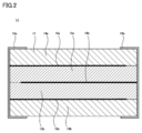
- FIG. 3 is a cross-sectional view of a main part of a piezoelectric element of the piezoelectric sensor according to Embodiment 1.
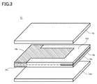
- FIG. 1 is an exploded perspective view of a main part of a piezoelectric sensor according to a first embodiment. It is explanatory drawing which shows the case where the piezoelectric sensor concerning Embodiment 1 is installed in the tire. It is explanatory drawing which showed typically the deformation
- FIG. 1 is a side view showing a piezoelectric sensor according to Embodiment 1.
- FIG. 3 is a cross-sectional view of a main part of a piezoelectric element of the piezoelectric sensor according to Embodiment 1.
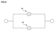
- FIG. 3 is an equivalent circuit diagram of the piezoelectric sensor according to the first embodiment.
- 6 is a side view of a piezoelectric sensor according to a second embodiment.
- FIG. It is explanatory drawing which showed typically the deformation
- FIG. 1 shows a piezoelectric sensor 100 according to the first embodiment.
- the piezoelectric sensor 100 includes a substrate 10 and a piezoelectric element 11 mounted on the substrate 10.
- the piezoelectric element 11 has a rectangular parallelepiped shape, and includes a stacked body 17, and first terminal electrodes 15 a and second terminal electrodes 15 b provided on both end faces of the stacked body 17.
- the first terminal electrode 15a and the second terminal electrode 15b are mounted on the substrate 10 by solders 19a and 19b, which are bonding materials, respectively.
- a gap 13 corresponding to the mounting height is formed.
- the laminated body 17 of the piezoelectric elements 11 includes, in order from the top, an exterior body 14a, a first detection electrode 16a, a piezoelectric body 12a, a second detection electrode 16b, a piezoelectric body 12b, and a first detection body.
- the electrode 16c and the outer package 14b are laminated and integrated.
- the piezoelectric body 12b on which the first detection electrode 16c is formed and the exterior body 14b are bonded and integrated with an adhesive (not shown).
- the piezoelectric bodies 12a and 12b are made of, for example, a ceramic material having piezoelectricity. Moreover, the exterior bodies 14a and 14b are formed of an insulating material such as a ceramic material such as magnesium titanate or a resin material such as glass epoxy. Each of the piezoelectric bodies 12a and 12b and the exterior bodies 14a and 14b has a rectangular flat plate shape. The piezoelectric bodies 12a and 12b are each subjected to polarization treatment.
- a structure in which the upper and lower main surfaces of the piezoelectric bodies 12a and 12b are held by the exterior bodies 14a and 14b is adopted.
- the displacement of the piezoelectric bodies 12a and 12b in the thickness direction is suppressed, even when an impact with acceleration is applied, detection of acceleration can be suppressed and deflection can be detected more accurately.
- the other main surface may be partially held, and the holding of the other main surface may be omitted.
- outer casings 14a and 14b having higher Young's modulus than piezoelectric bodies 12a and 12b.
- the first detection electrodes 16a and 16c are drawn out from one end face of the multilayer body 17 and two side faces following the both sides.
- the second detection electrode 16b is drawn to the outside from the other end face of the multilayer body 17 and two side faces that follow both sides thereof.
- the first detection electrodes 16 a and 16 c and the second detection electrode 16 b are each drawn out from the three surfaces of the stacked body 17 in a T shape.
- the electrical connection reliability is high.
- the second detection electrode 16b and the second terminal electrode 15b are connected not only at the end face but also at a part of the side face, the electrical connection reliability is high.
- the layered body 17 has a structure other than the connection portion with the first terminal electrode 15a and the second terminal electrode 15b. Not exposed to the outer surface. Therefore, it is not easily affected by the external environment such as moisture.
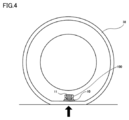
- FIG. 4 shows a state where the piezoelectric sensor 100 attached to the tire 38 on the substrate 10 side detects the deformation of the tire.
- the piezoelectric sensor 100 mainly detects the deflection of the substrate caused by the deformation of the tire 38 due to air pressure fluctuation or the deformation of the tire in the road surface state.
- the tire 38 when the tire 38 is grounded to the ground, the tire 38 is deformed, so that the substrate 10 bends vertically upward from the ground, and the deflection causes the piezoelectric element 11 to vertically upward from the ground. Bend.
- the amount of deflection of the substrate 10 and the piezoelectric element 11 depends on the amount of deformation of the tire 38.
- the tire 38 rotates in accordance with the progress of the mounted automobile or the like, and the portion where the piezoelectric sensor 100 is mounted is periodically grounded. Therefore, the piezoelectric sensor 100 can detect periodic tire deformation.
- the piezoelectric element 11 is mounted on the substrate 10 at two locations, a first terminal electrode 15a and a second terminal electrode 15b.
- the size of the substrate 10 is larger than the size of the piezoelectric element 11. Therefore, in the piezoelectric sensor 100, the deflection of the substrate 10 is amplified and the piezoelectric element 11 is bent. Then, the magnitude of the deflection of the piezoelectric element 11 is detected as an electrical signal from the first detection electrodes 16a and 16b and the second detection electrode 16b.
- the piezoelectric sensor 100 has high sensitivity because the deflection of the substrate 10 is amplified and the piezoelectric element 11 bends, and the deflection of the piezoelectric element 11 is detected as an electric signal.
- the piezoelectric sensor 100 has a gap 13 between the substrate 10 and the piezoelectric element 11.
- the gap 13 functions to prevent the piezoelectric sensor 100 from detecting noise such as external impact or vibration transmitted directly from the tire 38.
- the piezoelectric sensor 100 can detect only deflection with high sensitivity without detecting noise such as external impact and vibration.
- the piezoelectric sensor 100 Since the piezoelectric sensor 100 has high sensitivity, it can be formed in a small size. In addition, by mounting other electronic components on the substrate 10, it is easy to integrate peripheral circuits into a module.
- FIG. 5A shows a state in which no deflection is applied to the piezoelectric sensor 100.
- the piezoelectric sensor as in this embodiment is often used in an environment where severe temperature changes occur. For this reason, a phenomenon in which charges are generated by heat, that is, pyroelectricity, may occur, and the charges generated by the pyroelectricity may be mixed with the charges generated by the deflection. Therefore, it is preferable to reduce the influence of pyroelectricity.
- the terminal electrodes 15a and 15b and the detection electrodes 16a, 16b and 16c are provided, and detection is performed in two layers. 6 is configured so as not to be affected by pyroelectricity. In other words, this circuit cancels out the electric charge caused by pyroelectricity by connecting the two layers of detection parts in parallel. Therefore, it is possible to detect only the electric charge due to the deflection.
- the deformation as shown in FIG. 5B occurs in the piezoelectric sensor 100 when the deflection is acting.
- a tensile stress Pt is generated in the piezoelectric bodies 12a and 12b.
- the side on which the detection electrode 16a is provided and the side on which the detection electrode 16b is provided are positive (+) and negative (based on the relationship between the polarization direction and the tensile stress Pt ( -) Is generated.
- the side on which the detection electrode 16b is provided and the side on which the detection electrode 16c is provided are positive and negative based on the relationship between the polarization direction and the tensile stress Pt. Charge is generated.
- the piezoelectric sensor 100 according to the first embodiment having the above structure can be manufactured, for example, according to the following procedure.
- the detection electrodes 16a and 16b are formed on the piezoelectric body 12a such as ceramic, and the detection electrode 16c is formed on the piezoelectric body 12b such as ceramic by screen printing.
- a polarization process is performed in which the polarization direction becomes a desired direction.
- an adhesive such as an epoxy resin is applied to both main surfaces of the integrally fired piezoelectric bodies 12a and 12b, and the exterior body 14a, the piezoelectric bodies 12a and 12b, and the exterior body 14b are laminated and integrally joined. . Thereby, the laminated body 17 is produced.
- terminal electrodes 15a and 15b are formed by forming a thin film such as Ag on the both end faces of the laminated body 17 by sputtering or the like, and performing metal plating on the thin film. Thereby, the piezoelectric element 11 is obtained.
- the piezoelectric element 100 is completed by mounting the piezoelectric element 11 on the substrate 10 with solder.
- the first detection electrode and the second detection electrode are T-shaped, but it is not always necessary to make such a configuration.
- other shapes such as an I-shape are used. Can do.
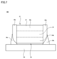
- FIG. 7 shows a piezoelectric sensor 200 according to the second embodiment.
- the piezoelectric sensor 200 includes a piezoelectric element 21 including a single piezoelectric body 22 instead of the piezoelectric element 11 of the first embodiment.
- the piezoelectric element 21 includes a multilayer body 27, and a first terminal electrode 25a and a second terminal electrode 25b.
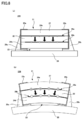
- the laminated body 27 includes an exterior body 24a, a first detection electrode 26a, a piezoelectric body 22, a second detection electrode 26b, and an exterior body 24b stacked in order from the top. It consists of the structure made.
- the first terminal electrode 25a and the second terminal electrode 25b are mounted on the substrate 20 by solders 29a and 29b, which are bonding materials, respectively.
- a gap 23 corresponding to the mounting height is formed.
- the outer body 24a, the piezoelectric body 22 in which the first detection electrode 26a is formed on one main surface and the second detection electrode 26b is formed on the other main surface, and the outer body 24b are bonded and integrated by an adhesive (not shown).
- the piezoelectric sensor 200 composed of the above has fewer piezoelectric bodies and detection electrodes, so that the piezoelectric sensor 200 can be easily produced at low cost.
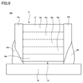
- FIG. 9 shows a piezoelectric sensor 300 according to the third embodiment.
- the piezoelectric sensor 300 includes a piezoelectric element 31 including three piezoelectric bodies 32a, 32b, and 32c instead of the piezoelectric element 11 of the first embodiment.
- the piezoelectric element 31 includes a stacked body 37, a first terminal electrode 35a, and a second terminal electrode 35b.
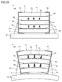
- the laminated body 37 includes, in order from the top, an exterior body 34a, a first detection electrode 36a, a piezoelectric body 32a, a second detection electrode 36b, a piezoelectric body 32b, and a first detection electrode.
- 36c, the piezoelectric body 32c, the second detection electrode 36d, and the exterior body 34b are stacked and integrated.
- the first terminal electrode 35a and the second terminal electrode 35b are mounted on the substrate 30 by solders 39a and 39b, which are bonding materials, respectively.
- a gap 33 corresponding to the height of the mounting is formed.
- the piezoelectric body 32b in which the first detection electrode 36c is formed, the piezoelectric body 32c in which the first detection electrode 36d is formed on one main surface, and the exterior body 34b are formed by an adhesive (not shown). Bonded and integrated.
- the piezoelectric bodies 32a, 32b, and 32c are each subjected to polarization treatment.
- the piezoelectric body 32b sandwiched between the piezoelectric bodies 32a and 32c does not function as a piezoelectric body, the piezoelectric body 32b can be an unpolarized piezoelectric body or an insulator.
- the piezoelectric sensor 300 can cancel the electric charge by pyroelectricity similarly to the piezoelectric sensor 100 according to the first embodiment.
- the piezoelectric element 31 is taller than the piezoelectric sensor 100 according to the first embodiment by the amount of the piezoelectric body 32b. For this reason, when the substrate 30 bends to the same extent as the substrate 10 of the first embodiment, the deflection of the piezoelectric body 32a becomes larger than that of the piezoelectric body 12a. Thereby, the sensitivity which detects a deflection
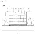
- FIG. 11 shows a piezoelectric sensor 400 according to the fourth embodiment.
- the gap 43 of the piezoelectric sensor 100 according to the first embodiment is filled with a resin 43.
- a resin 43 a silicone-based resin, rubber, or the like can be used.
- the bonding strength between the substrate 40 and the piezoelectric element 41 is improved as compared with the piezoelectric sensors 100, 200, and 300 according to the first to third embodiments.
- the piezoelectric sensor includes a substrate and a piezoelectric element.
- the substrate has a pair of mounting electrodes formed on one main surface.
- the piezoelectric element includes a laminate, and a first terminal electrode and a second terminal electrode provided on different end surfaces of the laminate.
- the laminated body includes a piezoelectric body, a first detection electrode and a second detection electrode provided so as to sandwich the piezoelectric body, and an outer side of at least one of the first detection electrode and the second detection electrode. And an insulating exterior body laminated on the substrate.
- the first detection electrode is connected to the first terminal electrode, and the second detection electrode is connected to the second terminal electrode.
- the first terminal electrode is bonded to one of the pair of mounting electrodes by a bonding material, and the second terminal electrode is bonded to the other of the pair of mounting electrodes by a bonding material. Thereby, the piezoelectric element is mounted on the substrate.
- the first detection electrode may be connected to the first terminal electrode by being pulled out from one end surface of the laminate and two side surfaces in contact with the end surface.
- the second detection electrode may be connected to the second terminal electrode by being drawn out from the other end face of the laminate and two side faces in contact with the end face.
- a gap may be formed between the substrate and the piezoelectric element.
- rubber or resin may be filled between the substrate and the piezoelectric element.
- the piezoelectric element includes a laminate, and a first terminal electrode and a second terminal electrode provided on different end surfaces of the laminate.
- the laminated body includes a piezoelectric body, a first detection electrode and a second detection electrode provided so as to sandwich the piezoelectric body, and an outer side of at least one of the first detection electrode and the second detection electrode. And an insulating exterior body laminated on the substrate.
- the first detection electrode is connected to the first terminal electrode
- the second detection electrode is connected to the second terminal electrode.
- Piezoelectric sensor 10 20, 30, 40 Substrate, 11, 21, 31, 41 Piezoelectric element, 12a, 12b, 22, 32a, 32b, 32c, 42a, 42b Piezoelectric body, 14a, 14b 24a, 24b, 34a, 34b, 44a, 44b exterior body, 15a, 15b, 25a, 25b, 35a, 35b, 45a, 45b terminal electrode, 16a, 16b, 16c, 26a, 26b, 36a, 36b, 36c, 36d 46a, 46b, 46c, electrode for detection, 17, 27, 37, 47 laminate, 38 tire, 19a, 19b, 29a, 29b, 39a, 39b, 49a, 49b solder, 13, 23, 33 gap, 43 resin.
Landscapes
- Physics & Mathematics (AREA)
- General Physics & Mathematics (AREA)
- Engineering & Computer Science (AREA)
- Mechanical Engineering (AREA)
- Measuring Fluid Pressure (AREA)
- Force Measurement Appropriate To Specific Purposes (AREA)
Abstract
圧電センサ(100)は、基板(10)と、圧電素子(11)とを備える。基板(10)には、一方の主面に少なくとも1対の実装用電極が形成される。圧電素子(11)は、積層体(17)と、第1端子電極(15a)および第2端子電極(15b)とを備える。第1端子電極(15a)および第2端子電極(15b)は、それぞれ接合材(19a,19b)により、実装用電極に接合される。
Description
本発明は、圧電センサおよび圧電素子に関する。
従来、たわみを検出する圧電センサとして、たとえば特開2007-163230号公報(特許文献1)に記載の圧電センサが知られている。この圧電センサは、可撓制を有するポリイミドなどの高分子材料からなるフィルム状の平板の一方の主面に、窒化アルミニウムなどの薄膜状の圧電体を形成し、かつ、圧電体が形成された平板の両主面に電極層を設けることで構成されている。
この圧電センサは、極めて薄いフィルム状で柔軟性に富んでおり、タイヤ内面などの曲面部分に密着配置して用いられる。これにより、タイヤの空気圧の変動などによるタイヤの変形を検出することができる。
しかしながら、上記特開2007-163230号公報に記載の圧電センサにおいては、次のような問題があった。
当該公報に記載の圧電センサは、薄膜状の圧電体を備え、接着剤で、タイヤに直接貼り付けて用いられていた。よって、空気圧の変動によるタイヤの変形による信号以外にも、タイヤから直接的に伝わる外部衝撃や振動などさまざまな信号も同時に検出しやすかった。そのため、空気圧変動による変形だけを正確に検出するには、複雑な信号処理回路が必要であった。
さらに、当該公報に記載の圧電センサは、接着剤でタイヤに直接貼り付けて用いられているので、圧電センサ周辺に取り付けられる信号処理回路などの周辺回路装置は、多数のリード線などで接続されていた。これより、タイヤ内部の配線数が多く、また配線が長いために複雑になり、他の電子部品(たとえばICなど)を実装して使用することが困難であった。
また、フィルム状の圧電センサは非常に薄い構造をとることが可能であるが、一方で、感度をあげるために圧電センサ自体の面積を大きくし、大型化しなければならなかった。そのため、タイヤに釘などの鋭利なものが刺さった場合、圧電センサ自体や周辺回路装置が傷つけられる可能性が高く、傷つけられた場合、タイヤの変形を検出することができなくなった。
そこで、上記課題を解決するために、本発明の圧電センサは、基板と、圧電素子とを備え、基板は、一方の主面に実装用電極が形成され、圧電素子は、積層体と、積層体の互いに異なる端面に設けられた第1端子電極と第2端子電極とを備え、積層体は、圧電体と、圧電体を挟むように設けられた第1検出用電極、第2検出用電極、更に少なくとも一方の外側に積層された外装体とを備え、第1検出用電極は第1端子電極に接続され、第2検出用電極は第2端子電極に接続され、第1端子電極および第2端子電極が、接合剤により、それぞれ実装用電極に接合されて、圧電素子が基板に実装されるようにした。
なお、第1検出用電極は、積層体の一方の端面およびその端面に接する2つの側面から引き出されて、第1端子電極に接続され、第2検出用電極は、積層体の他方の端面およびその端面に接する2つの側面から引き出されて、第2端子電極に接続されることが好ましい。この場合には、検出用電極と端子電極との接続が確実になる。
また、基板と圧電素子との間に隙間が形成されることが好ましい。この場合には、隙間が、圧電センサが、タイヤ等から直接的に伝わる外部衝撃や振動などのノイズを検出するのを抑制ため、基板のたわみを高感度に検出することが可能になる。なお、隙間には、ゴムまたは樹脂を充填しても良い。この場合には、基板と圧電素子との接合強度が向上する。
また、本発明は、圧電素子にも向けられる。具体的には、圧電素子は、積層体と、積層体の互いに異なる端面に設けられた第1端子電極と第2端子電極とを備え、積層体は、圧電体と、圧電体を挟むように設けられた第1検出用電極、第2検出用電極、更に少なくとも一方の外側に積層された外装体とを備え、第1検出用電極は第1端子電極に接続され、第2検出用電極は第2端子電極に接続されるようにした。
本発明によれば、感度が高く、振動などのノイズを検出しにくく、小型化が容易で、モジュール化することにより周辺回路を一体化することも容易な圧電センサを提供することができる。
以下において、本発明の実施形態にかかる圧電センサについて、図面を参照しながら説明する。
(実施形態1)
図1に、実施形態1にかかる圧電センサ100を示す。圧電センサ100は、基板10と、基板10に実装された圧電素子11とを備えている。
図1に、実施形態1にかかる圧電センサ100を示す。圧電センサ100は、基板10と、基板10に実装された圧電素子11とを備えている。
圧電素子11は、直方体状をなしており、積層体17と、積層体17の両端面に設けられた第1端子電極15aおよび第2端子電極15bとを有する。第1端子電極15aおよび第2端子電極15bは、それぞれ接合材であるはんだ19a,19bによって基板10に実装されており、実装箇所以外の部分の基板10と圧電素子11との間には、はんだ実装の高さ分の隙間13が形成されている。
圧電素子11の積層体17は、図2に示すように、上から順に、外装体14a、第1検出用電極16a、圧電体12a、第2検出用電極16b、圧電体12b、第1検出用電極16c、外装体14bが積層され、一体化された構造からなる。
より具体的には、外装体14aと、一方の主面に第1検出用電極16aが形成され、他方の主面に第2検出用電極16bが形成された圧電体12aと、一方の主面に第1検出用電極16cが形成された圧電体12bと、外装体14bとが、接着剤(図示せず)により接着されて一体化されている。
なお、圧電体12a,12bは、例えば、圧電性を備えたセラミック材料により形成されている。また、外装体14a,14bは、例えば、チタン酸マグネシウム等のセラミック材料や、ガラスエポキシ等の樹脂材料といった絶縁性をもった材料により形成されている。圧電体12a,12bおよび外装体14a,14bは、それぞれ矩形平板状である。また、圧電体12a,12bには、それぞれ分極処理が施されている。
本実施形態では、圧電体12a,12bの上下両主面が外装体14a,14bによって保持されている構造を採用している。これにより、圧電体12a,12bの厚み方向の変位が抑制されるため、加速度を伴う衝撃を受けた場合でも、加速度の検出を抑え、たわみをより精度よく検出することが可能になる。圧電体12a,12bの一方の主面が全面で保持されていれば、他方の主面は部分的な保持であっても良いし、更には他方の主面の保持は省略しても良い。
なお、たわみ検出の感度を上げ、更により精度よく検出するためには、外装体14a,14bとして、圧電体12a,12bよりもヤング率の高いものを用いることが好ましい。
本実施形態の圧電センサ100においては、第1検出用電極16a,16cが、積層体17の一方の端面、および、その両側に続く2つの側面から外部に引き出されている。同様に、第2検出用電極16bが、積層体17の他方の端面、および、その両側に続く2つの側面から外部に引き出されている。
すなわち、図3に示すように、第1検出用電極16a,16c、および第2検出用電極16bは、それぞれ、T字状に、積層体17の3つの面から外部に引き出されている。
したがって、第1検出用電極16a,16cと第1端子電極15aとは、端面だけでなく側面の一部でも接続されているため、電気的な接続信頼性が高い。また、第2検出用電極16bと第2端子電極15bとは、端面だけでなく側面の一部でも接続されているため、電気的な接続信頼性が高い。また、第1検出用電極16a,16c、および第2検出用電極16bは、それぞれ、T字状であるため、第1端子電極15aおよび第2端子電極15bとの接続部以外では積層体17の外表面に露出しない。そのため、湿気等の外部環境の影響を受けにくい。
図4は、タイヤ38に基板10側で取り付けられた圧電センサ100が、タイヤの変形を検出している状態を示す。圧電センサ100は、主に、空気圧変動によるタイヤ38の変形や路面状態におけるタイヤの変形によって生じる基板のたわみを検知する。
図4に示すように、タイヤ38を地面に接地させた場合には、タイヤ38が変形するため、基板10が地面から垂直上向き方向にたわみ、そのたわみが圧電素子11を地面から垂直上向き方向にたわませる。基板10および圧電素子11のたわみの大きさは、タイヤ38の変形の大きさに依存する。
なお、タイヤ38は取り付けられた自動車などの進行に合わせて回転し、圧電センサ100の取り付けられた部分は周期的に接地する。したがって、圧電センサ100は、周期的なタイヤの変形を検出することが可能である。
図1に示すように、圧電センサ100は、圧電素子11が、第1端子電極15aと第2端子電極15bとの二ヵ所で基板10に実装されている。そして、平面方向に見た場合、基板10の大きさは圧電素子11の大きさよりも大きい。したがって、圧電センサ100では、基板10のたわみが、増幅されて圧電素子11をたわませる。そして、圧電素子11のたわみの大きさを、第1検出用電極16a,16b、および第2検出用電極16bから電気信号として検出する。圧電センサ100は、基板10のたわみが増幅されて圧電素子11がたわみ、その圧電素子11のたわみを電気信号として検出するため感度が高い。
また、図1に示すように、圧電センサ100は、基板10と圧電素子11との間に隙間13が形成されている。この隙間13は、圧電センサ100が、タイヤ38から直接的に伝わる外部衝撃や振動などのノイズを検出しないようにする機能を果たす。圧電センサ100は、外部衝撃や振動などのノイズを検出せず、たわみのみを高感度に検出することが可能になっている。
圧電センサ100は、感度が高いので、小型に形成することができる。また、基板10に他の電子部品を実装することで、周辺回路を一体化してモジュール化することも容易である。
次に、たわみの有無における電荷の発生の理論について、図5と図6とを用いて説明する。
図5(a)は、圧電センサ100に、たわみが作用していない状態を示す。本実施形態のような圧電センサは、苛酷な温度変化が生じる環境で使用されることが多い。その為、熱によって、電荷が発生する現象、すなわち焦電が起きることがあり、この焦電によって発生した電荷が、たわみによって発生した電荷と混合されてしまうことがある。その為、焦電による影響は、少なくすることが好ましい。
そこで、本実施形態の圧電センサ100では、図5(a)に示すように、端子電極15a,15bと、検出用電極16a,16b,16cと、を設け、2層で検出することにより、図6に示すような回路を構成し、焦電による影響を受けないようにしている。すなわち、この回路は、2層の検知部分を並列に接続することにより、焦電による電荷を打ち消すようにしている。したがって、たわみによる電荷のみを検出することが可能になっている。
一方で、たわみが作用している場合の圧電センサ100には、図5(b)に示すような変形が生じる。図5(b)に示すように、圧電体12a,12bには引っ張り応力Ptが発生する。圧電体12aでは、検出用電極16aが設けられている側と、検出用電極16bが設けられている側とには、分極方向と引っ張り応力Ptとの関係に基づいて正(+)および負(-)の電荷が発生する。同様に、圧電体12bでは、検出用電極16bが設けられている側と、検出用電極16cが設けられている側とには、分極方向と引っ張り応力Ptとの関係に基づいて、正および負電荷が発生する。
これより、端子電極15aには、検出用電極16aが設けられている側に発生した正電荷と、検出用電極16cが設けられている側に発生した負電荷とが伝わるが、検出用電極16cが設けられている側に発生した負電荷は比較的小さいために、検出用電極16aが設けられている側に発生した正電荷と打ち消しあい、結果として正電荷が端子電極15aに伝わる。同様に、端子電極15bには、検出用電極16bが設けられている側に発生した負電荷と正電荷とが伝わるが、正電荷は比較的小さいために、負電荷と打ち消しあい、結果として残りの負電荷が端子電極15bに伝わる。これより、両端面に電位差が生じ、基板のたわみを検知することが可能となる。
以上の構造からなる実施形態1にかかる圧電センサ100は、例えば、以下の手順に従って作製することができる。
まず、セラミックなどの圧電体12aに検出用電極16a,16bを、またセラミックなどの圧電体12bに検出用電極16cを、それぞれスクリーン印刷によって形成する。
次に、圧電体12a,12bを一体焼成した後、分極方向が所望の向きとなる分極処理を施す。
その後、一体焼成された圧電体12a,12bの両主面にエポキシ樹脂などの接着剤を塗り、外装体14aと、圧電体12a,12bと、外装体14bとを、積層して一体に接合する。これより、積層体17が作製される。
次に、積層体17の両端面に、スパッタリング法などにより、例えばAgなどの薄膜を形成し、その薄膜上に金属めっきを施すなどして、端子電極15a,15bを形成する。これより、圧電素子11が得られる。
最後に、圧電素子11を基板10にはんだで実装することで圧電センサ100を完成させる。
本実施形態においては、第1検出用電極および第2検出用電極をT字状としたが、必ずしもそのように構成する必要はなく、変形例としては、I字状など他の形状とすることができる。
(実施形態2)
図7に、実施形態2にかかる圧電センサ200を示す。
図7に、実施形態2にかかる圧電センサ200を示す。
圧電センサ200は、実施形態1の圧電素子11に代えて、一枚の圧電体22からなる圧電素子21を備えている。圧電素子21は、実施形態1と同様に、積層体27と、第1端子電極25aおよび第2端子電極25bとを有する。積層体27は、図8(a)に示すように、上から順に、外装体24a、第1検出用電極26a、圧電体22、第2検出用電極26b、外装体24bが積層され、一体化された構造からなる。第1端子電極25aおよび第2端子電極25bは、それぞれ接合材であるはんだ29a、29bによって基板20に実装されており、実装箇所以外の部分の基板20と圧電素子21との間には、はんだ実装の高さ分の隙間23が形成されている。
より具体的には、外装体24aと、一方の主面に第1検出用電極26aが形成され、他方の主面に第2検出用電極26bが形成された圧電体22と、外装体24bとが、接着剤(図示せず)により接着されて一体化されている。
以上よりなる圧電センサ200は、実施形態1と比較すると、使用する圧電体や検出用電極の数が少ない為、低コストかつ簡単に圧電センサ200を作成することが可能である。
(実施形態3)
図9に、実施形態3にかかる圧電センサ300を示す。
図9に、実施形態3にかかる圧電センサ300を示す。
圧電センサ300は、実施形態1の圧電素子11に代えて、三枚の圧電体32a,32b,32cからなる圧電素子31を備えている。圧電素子31は、実施形態1と同様に、積層体37と、第1端子電極35aおよび第2端子電極35bとを有する。積層体37は、図10(a)に示すように、上から順に、外装体34a、第1検出用電極36a、圧電体32a、第2検出用電極36b、圧電体32b、第1検出用電極36c、圧電体32c、第2検出用電極36d、外装体34bが積層され、一体化された構造からなる。第1端子電極35aおよび第2端子電極35bは、それぞれ接合材であるはんだ39a、39bによって基板30に実装されており、実装箇所以外の部分の基板30と圧電素子31との間には、はんだ実装の高さ分の隙間33が形成されている。
より具体的には、外装体34aと、一方の主面に第1検出用電極36aが形成され、他方の主面に第2検出用電極36bが形成された圧電体32aと、一方の主面に第1検出用電極36cが形成された圧電体32bと、一方の主面に第1検出用電極36dが形成された圧電体32cと、外装体34bとが、接着剤(図示せず)により接着されて一体化されている。
圧電体32a,32b,32cには、それぞれ分極処理が施されている。ここで、圧電体32a,32cに挟まれた圧電体32bは、圧電体として機能しないため、圧電体32bは分極処理していない圧電体、または絶縁体を用いることもできる。
なお、圧電センサ300も、第1実施形態にかかる圧電センサ100と同様に、焦電による電荷を打ち消すことができる。
本実施形態にかかる圧電センサ300は、実施形態1にかかる圧電センサ100と比較して、圧電体32b分だけ圧電素子31の背が高い。この為、実施形態1の基板10と同程度に基板30がたわんだ際に、圧電体32aのたわみは圧電体12aのたわみよりも大きくなる。これにより、たわみを検出する感度が高くなっている。
(実施形態4)
図11に、実施形態4にかかる圧電センサ400を示す。
図11に、実施形態4にかかる圧電センサ400を示す。
圧電センサ400は、実施形態1にかかる圧電センサ100の隙間13に、樹脂43が充填されている。樹脂43は、シリコーン系樹脂やゴムなどを用いることが可能である。
本実施形態にかかる圧電センサ400は、実施形態1ないし3にかかる圧電センサ100,200,300と比較して、基板40と圧電素子41との接合強度が向上している。
(実施形態の要約)
以上において例示した種々の実施形態にかかる圧電センサの特徴的な構成を要約すると、以下のとおりとなる。
以上において例示した種々の実施形態にかかる圧電センサの特徴的な構成を要約すると、以下のとおりとなる。
圧電センサは、基板と、圧電素子と、を備える。上記基板は、一方の主面に一対の実装用電極が形成される。上記圧電素子は、積層体と、上記積層体の互いに異なる端面に設けられた第1端子電極および第2端子電極とを有する。上記積層体は、圧電体と、上記圧電体を挟むように設けられた第1検出用電極および第2検出用電極と、上記第1検出用電極および上記第2検出用電極の少なくとも一方の外側に積層された絶縁性の外装体とを含む。上記第1検出用電極は、上記第1端子電極に接続され、上記第2検出用電極は、上記第2端子電極に接続される。上記第1端子電極は、接合材によって上記一対の実装用電極の一方に接合されるとともに、上記第2端子電極は、接合材によって上記一対の実装用電極の他方に接合される。これにより、上記圧電素子は、上記基板に実装される。
また、上記圧電センサにあっては、上記第1検出用電極が、上記積層体の一方の端面および当該端面に接する2つの側面から引き出されることにより、上記第1端子電極に接続されてもよく、上記第2検出用電極が、上記積層体の他方の端面および当該端面に接する2つの側面から引き出されることにより、上記第2端子電極に接続されてもよい。
また、上記圧電センサにあっては、上記基板と上記圧電素子との間に隙間が形成されてもよい。
また、上記圧電センサにあっては、上記基板と上記圧電素子との間にゴムまたは樹脂が充填されてもよい。
また、以上において例示した種々の実施形態にかかる圧電素子の特徴的な構成を要約すると以下のとおりとなる。
圧電素子は、積層体と、上記積層体の互いに異なる端面に設けられた第1端子電極および第2端子電極と、を備える。上記積層体は、圧電体と、上記圧電体を挟むように設けられた第1検出用電極および第2検出用電極と、上記第1検出用電極および上記第2検出用電極の少なくとも一方の外側に積層された絶縁性の外装体と、を含む。上記第1検出用電極は、上記第1端子電極に接続され、上記第2検出用電極は、上記第2端子電極に接続さる。
今回開示した上記実施形態はすべての点で例示であって、制限的なものではない。本発明の技術的範囲は請求の範囲によって画定され、また請求の範囲の記載と均等の意味および範囲内でのすべての変更を含むものである。
100,200,300,400 圧電センサ、10,20,30,40 基板、11,21,31,41 圧電素子、12a,12b,22,32a,32b,32c,42a,42b 圧電体、14a,14b,24a,24b,34a,34b,44a,44b 外装体、15a,15b,25a,25b,35a,35b,45a,45b 端子電極、16a,16b,16c,26a,26b,36a,36b,36c,36d,46a,46b,46c 検出用電極、17,27,37,47 積層体、38 タイヤ、19a,19b,29a,29b,39a,39b,49a,49b はんだ、13,23,33 隙間、43 樹脂。
Claims (5)
- 相対して位置する第1端面および第2端面を含む積層体と、
前記第1端面に設けられた第1端子電極と、
前記第2端面に設けられた第2端子電極と、を備え、
前記積層体は、圧電体と、前記第1端面および前記第2端面を結ぶ方向と直交する方向において前記圧電体を挟むように前記圧電体に積層された第1検出用電極および第2検出用電極と、前記第1検出用電極および前記第2検出用電極の少なくとも一方の外側に位置するようにさらに積層された絶縁性の外装体とを含み、
前記第1検出用電極が、前記第1端子電極に接続されているとともに、前記第2検出用電極が、前記第2端子電極に接続されている、圧電素子。 - 前記積層体は、当該積層体における積層方向と前記第1端面および前記第2端面を結ぶ方向とのいずれにも直交する方向に位置する一対の側面を含み、
前記第1検出用電極が、前記第1端面と前記一対の側面とに引き出されて前記第1端子電極に接続されているとともに、前記第2検出用電極が、前記第2端面と前記一対の側面とに引き出されて前記第2端子電極に接続されている、請求項1に記載の圧電素子。 - 請求項1または2に記載の圧電素子と、
前記圧電素子が実装された基板と、を備え、
前記基板は、前記圧電素子が位置する側の主面に一対の実装用電極を有し、
前記第1端子電極が、前記一対の実装用電極の一方に接合材を介して接合されているとともに、前記第2端子電極が前記一対の実装用電極の他方に接合材を介して接合されている、圧電センサ。 - 前記圧電素子と前記基板との間に隙間が形成されている、請求項3に記載の圧電センサ。
- 前記圧電素子と前記基板との間にゴムまたは樹脂が充填されている、請求項3に記載の圧電センサ。
Priority Applications (3)
| Application Number | Priority Date | Filing Date | Title |
|---|---|---|---|
| JP2016531136A JP6252678B2 (ja) | 2014-07-04 | 2015-03-17 | 圧電センサおよび圧電素子 |
| CN201580033288.5A CN106461486B (zh) | 2014-07-04 | 2015-03-17 | 压电传感器及压电元件 |
| US15/386,148 US10232674B2 (en) | 2014-07-04 | 2016-12-21 | Piezoelectric sensor and piezoelectric element |
Applications Claiming Priority (2)
| Application Number | Priority Date | Filing Date | Title |
|---|---|---|---|
| JP2014-138751 | 2014-07-04 | ||
| JP2014138751 | 2014-07-04 |
Related Child Applications (1)
| Application Number | Title | Priority Date | Filing Date |
|---|---|---|---|
| US15/386,148 Continuation US10232674B2 (en) | 2014-07-04 | 2016-12-21 | Piezoelectric sensor and piezoelectric element |
Publications (1)
| Publication Number | Publication Date |
|---|---|
| WO2016002262A1 true WO2016002262A1 (ja) | 2016-01-07 |
Family
ID=55018823
Family Applications (1)
| Application Number | Title | Priority Date | Filing Date |
|---|---|---|---|
| PCT/JP2015/057866 Ceased WO2016002262A1 (ja) | 2014-07-04 | 2015-03-17 | 圧電センサおよび圧電素子 |
Country Status (4)
| Country | Link |
|---|---|
| US (1) | US10232674B2 (ja) |
| JP (1) | JP6252678B2 (ja) |
| CN (1) | CN106461486B (ja) |
| WO (1) | WO2016002262A1 (ja) |
Cited By (2)
| Publication number | Priority date | Publication date | Assignee | Title |
|---|---|---|---|---|
| CN107026230A (zh) * | 2016-01-29 | 2017-08-08 | Tdk株式会社 | 压电致动器 |
| JP2022159314A (ja) * | 2018-12-17 | 2022-10-17 | アルプスアルパイン株式会社 | タイヤセンサモジュールおよびタイヤセンサ装置 |
Families Citing this family (8)
| Publication number | Priority date | Publication date | Assignee | Title |
|---|---|---|---|---|
| CN106461486B (zh) * | 2014-07-04 | 2019-06-28 | 株式会社村田制作所 | 压电传感器及压电元件 |
| JP2018173343A (ja) * | 2017-03-31 | 2018-11-08 | セイコーエプソン株式会社 | 力検出装置およびロボット |
| CN112236657A (zh) * | 2018-07-06 | 2021-01-15 | 欧姆龙株式会社 | 应变传感器和拉伸特性测定方法 |
| WO2020131539A1 (en) * | 2018-12-21 | 2020-06-25 | Bridgestone Americas Tire Operations, Llc | Tire deflection sensing system |
| CN109696458B (zh) * | 2019-02-19 | 2024-04-26 | 泰安博联物联网科技有限公司 | 基于利用压电检测法的正负x面检测装置及检测方法 |
| AU2021224844A1 (en) * | 2020-02-21 | 2022-10-20 | Nitto Bend Technologies, Inc. | Tire and tire sensor |
| CN112124013A (zh) * | 2020-08-25 | 2020-12-25 | 江苏理工学院 | 一种基于压电发电材料的智能轮胎测试系统及测试方法 |
| US12459311B2 (en) * | 2021-10-30 | 2025-11-04 | Tdk Corporation | Devices and methods for overloading protection of piezoelectric material mounted on wheels |
Citations (4)
| Publication number | Priority date | Publication date | Assignee | Title |
|---|---|---|---|---|
| JP2000114912A (ja) * | 1998-09-30 | 2000-04-21 | Murata Mfg Co Ltd | 圧電部品 |
| JP2007315958A (ja) * | 2006-05-26 | 2007-12-06 | Tdk Corp | 加速度センサおよび加速度センサの製造方法 |
| JP2011525046A (ja) * | 2008-06-19 | 2011-09-08 | エプコス アクチエンゲゼルシャフト | 圧電素子、及び電気的接続の形成方法 |
| JP2013101020A (ja) * | 2011-11-08 | 2013-05-23 | Seiko Epson Corp | センサー素子、力検出装置およびロボット |
Family Cites Families (16)
| Publication number | Priority date | Publication date | Assignee | Title |
|---|---|---|---|---|
| JPH0663725B2 (ja) | 1985-12-27 | 1994-08-22 | ダイキン工業株式会社 | 圧電センサ |
| US5786655A (en) * | 1994-05-26 | 1998-07-28 | Canon Kabushiki Kaisha | Strain element and vibration device |
| DE10026005B4 (de) * | 2000-05-25 | 2004-07-08 | Robert Bosch Gmbh | Piezoaktor |
| US6664716B2 (en) * | 2000-06-07 | 2003-12-16 | Purdue Research Foundation | Piezoelectric transducer |
| US6800986B2 (en) * | 2002-01-23 | 2004-10-05 | Tdk Corporation | Piezoelectric sensor |
| JP2004128386A (ja) * | 2002-10-07 | 2004-04-22 | Nec Tokin Corp | 積層型圧電セラミックス素子 |
| JP4427665B2 (ja) | 2004-07-28 | 2010-03-10 | 国立大学法人広島大学 | 曲げ変形センサおよび変形測定装置 |
| JP2006048302A (ja) | 2004-08-03 | 2006-02-16 | Sony Corp | 圧電複合装置、その製造方法、その取扱方法、その制御方法、入出力装置及び電子機器 |
| JP2007010377A (ja) * | 2005-06-28 | 2007-01-18 | Kyocera Corp | 加速度センサ |
| JP5168681B2 (ja) | 2005-12-12 | 2013-03-21 | 独立行政法人産業技術総合研究所 | タイヤ空気圧センサおよびタイヤ空気圧監視装置 |
| JP6016228B2 (ja) * | 2012-07-03 | 2016-10-26 | ソニーセミコンダクタソリューションズ株式会社 | センサデバイス |
| JP2014052263A (ja) * | 2012-09-06 | 2014-03-20 | Nippon Dempa Kogyo Co Ltd | 外力検出装置及び外力検出センサー |
| CN105247331A (zh) * | 2013-05-01 | 2016-01-13 | 索尼公司 | 传感器装置和电子设备 |
| CN106461486B (zh) * | 2014-07-04 | 2019-06-28 | 株式会社村田制作所 | 压电传感器及压电元件 |
| CN107208999B (zh) * | 2015-02-18 | 2019-07-23 | 株式会社村田制作所 | 压电传感器 |
| JP2018129629A (ja) * | 2017-02-07 | 2018-08-16 | セイコーエプソン株式会社 | 圧電センサー及び圧電デバイス |
-
2015
- 2015-03-17 CN CN201580033288.5A patent/CN106461486B/zh not_active Expired - Fee Related
- 2015-03-17 WO PCT/JP2015/057866 patent/WO2016002262A1/ja not_active Ceased
- 2015-03-17 JP JP2016531136A patent/JP6252678B2/ja not_active Expired - Fee Related
-
2016
- 2016-12-21 US US15/386,148 patent/US10232674B2/en active Active
Patent Citations (4)
| Publication number | Priority date | Publication date | Assignee | Title |
|---|---|---|---|---|
| JP2000114912A (ja) * | 1998-09-30 | 2000-04-21 | Murata Mfg Co Ltd | 圧電部品 |
| JP2007315958A (ja) * | 2006-05-26 | 2007-12-06 | Tdk Corp | 加速度センサおよび加速度センサの製造方法 |
| JP2011525046A (ja) * | 2008-06-19 | 2011-09-08 | エプコス アクチエンゲゼルシャフト | 圧電素子、及び電気的接続の形成方法 |
| JP2013101020A (ja) * | 2011-11-08 | 2013-05-23 | Seiko Epson Corp | センサー素子、力検出装置およびロボット |
Cited By (7)
| Publication number | Priority date | Publication date | Assignee | Title |
|---|---|---|---|---|
| CN107026230A (zh) * | 2016-01-29 | 2017-08-08 | Tdk株式会社 | 压电致动器 |
| CN107026230B (zh) * | 2016-01-29 | 2019-09-10 | Tdk株式会社 | 压电致动器 |
| US10439126B2 (en) | 2016-01-29 | 2019-10-08 | Tdk Corporation | Piezoelectric actuator |
| JP2022159314A (ja) * | 2018-12-17 | 2022-10-17 | アルプスアルパイン株式会社 | タイヤセンサモジュールおよびタイヤセンサ装置 |
| CN116182695A (zh) * | 2018-12-17 | 2023-05-30 | 阿尔卑斯阿尔派株式会社 | 轮胎传感器模块以及轮胎传感器装置 |
| JP7366203B2 (ja) | 2018-12-17 | 2023-10-20 | アルプスアルパイン株式会社 | タイヤセンサモジュールおよびタイヤセンサ装置 |
| US12207558B2 (en) | 2018-12-17 | 2025-01-21 | Alps Alpine Co., Ltd. | Composite piezoelectric element, tire-condition measuring apparatus, tire sensor module, tire sensor, and piezoelectric sensor |
Also Published As
| Publication number | Publication date |
|---|---|
| CN106461486A (zh) | 2017-02-22 |
| CN106461486B (zh) | 2019-06-28 |
| JPWO2016002262A1 (ja) | 2017-04-27 |
| US20170190227A1 (en) | 2017-07-06 |
| US10232674B2 (en) | 2019-03-19 |
| JP6252678B2 (ja) | 2017-12-27 |
Similar Documents
| Publication | Publication Date | Title |
|---|---|---|
| JP6252678B2 (ja) | 圧電センサおよび圧電素子 | |
| US10429255B2 (en) | Piezoelectric sensor and detecting device | |
| CN108291796B (zh) | 压电挠曲传感器以及检测装置 | |
| CN101501505B (zh) | 复合传感器 | |
| JP5950053B2 (ja) | 押圧検出センサ | |
| US11906373B2 (en) | Pressure sensor and electronic equipment | |
| JP6004123B2 (ja) | 圧電センサの製造方法 | |
| CN108291795A (zh) | 压电挠曲传感器 | |
| JP6079931B2 (ja) | 押圧センサ | |
| JP2014013207A (ja) | 複合センサ | |
| US10502542B2 (en) | Piezoelectric element and piezoelectric sensor | |
| JPWO2008093680A1 (ja) | 加速度センサ | |
| JP6052434B2 (ja) | 圧電センサの製造方法 | |
| JP5049253B2 (ja) | 半導体素子 | |
| US9404938B2 (en) | Acceleration sensor | |
| JP2007183147A (ja) | 振動素子およびこの振動素子を用いた角速度センサ | |
| JP2014021065A (ja) | 物理量センサ | |
| JP2014157063A (ja) | 複合センサ素子 | |
| JP2014153188A (ja) | 焦電センサ | |
| JP2015021922A (ja) | 力学量センサ | |
| JP2015034720A (ja) | 振動片、電子機器、移動体、振動片の製造方法 | |
| JP2010085295A (ja) | Memsセンサ |
Legal Events
| Date | Code | Title | Description |
|---|---|---|---|
| 121 | Ep: the epo has been informed by wipo that ep was designated in this application |
Ref document number: 15815502 Country of ref document: EP Kind code of ref document: A1 |
|
| ENP | Entry into the national phase |
Ref document number: 2016531136 Country of ref document: JP Kind code of ref document: A |
|
| NENP | Non-entry into the national phase |
Ref country code: DE |
|
| 122 | Ep: pct application non-entry in european phase |
Ref document number: 15815502 Country of ref document: EP Kind code of ref document: A1 |