WO2015199163A1 - 撮像センサおよび撮像装置 - Google Patents
撮像センサおよび撮像装置 Download PDFInfo
- Publication number
- WO2015199163A1 WO2015199163A1 PCT/JP2015/068280 JP2015068280W WO2015199163A1 WO 2015199163 A1 WO2015199163 A1 WO 2015199163A1 JP 2015068280 W JP2015068280 W JP 2015068280W WO 2015199163 A1 WO2015199163 A1 WO 2015199163A1
- Authority
- WO
- WIPO (PCT)
- Prior art keywords
- filter
- signal
- band
- wavelength band
- infrared
- Prior art date
- Legal status (The legal status is an assumption and is not a legal conclusion. Google has not performed a legal analysis and makes no representation as to the accuracy of the status listed.)
- Ceased
Links
Images






















Classifications
-
- H—ELECTRICITY
- H04—ELECTRIC COMMUNICATION TECHNIQUE
- H04N—PICTORIAL COMMUNICATION, e.g. TELEVISION
- H04N23/00—Cameras or camera modules comprising electronic image sensors; Control thereof
- H04N23/80—Camera processing pipelines; Components thereof
- H04N23/84—Camera processing pipelines; Components thereof for processing colour signals
- H04N23/88—Camera processing pipelines; Components thereof for processing colour signals for colour balance, e.g. white-balance circuits or colour temperature control
-
- G—PHYSICS
- G02—OPTICS
- G02B—OPTICAL ELEMENTS, SYSTEMS OR APPARATUS
- G02B5/00—Optical elements other than lenses
- G02B5/20—Filters
- G02B5/201—Filters in the form of arrays
-
- G—PHYSICS
- G02—OPTICS
- G02B—OPTICAL ELEMENTS, SYSTEMS OR APPARATUS
- G02B5/00—Optical elements other than lenses
- G02B5/20—Filters
-
- G—PHYSICS
- G02—OPTICS
- G02B—OPTICAL ELEMENTS, SYSTEMS OR APPARATUS
- G02B5/00—Optical elements other than lenses
- G02B5/20—Filters
- G02B5/208—Filters for use with infrared or ultraviolet radiation, e.g. for separating visible light from infrared and/or ultraviolet radiation
-
- H—ELECTRICITY
- H04—ELECTRIC COMMUNICATION TECHNIQUE
- H04N—PICTORIAL COMMUNICATION, e.g. TELEVISION
- H04N23/00—Cameras or camera modules comprising electronic image sensors; Control thereof
- H04N23/10—Cameras or camera modules comprising electronic image sensors; Control thereof for generating image signals from different wavelengths
- H04N23/11—Cameras or camera modules comprising electronic image sensors; Control thereof for generating image signals from different wavelengths for generating image signals from visible and infrared light wavelengths
-
- H—ELECTRICITY
- H04—ELECTRIC COMMUNICATION TECHNIQUE
- H04N—PICTORIAL COMMUNICATION, e.g. TELEVISION
- H04N23/00—Cameras or camera modules comprising electronic image sensors; Control thereof
- H04N23/10—Cameras or camera modules comprising electronic image sensors; Control thereof for generating image signals from different wavelengths
- H04N23/12—Cameras or camera modules comprising electronic image sensors; Control thereof for generating image signals from different wavelengths with one sensor only
-
- H—ELECTRICITY
- H04—ELECTRIC COMMUNICATION TECHNIQUE
- H04N—PICTORIAL COMMUNICATION, e.g. TELEVISION
- H04N23/00—Cameras or camera modules comprising electronic image sensors; Control thereof
- H04N23/20—Cameras or camera modules comprising electronic image sensors; Control thereof for generating image signals from infrared radiation only
- H04N23/21—Cameras or camera modules comprising electronic image sensors; Control thereof for generating image signals from infrared radiation only from near infrared [NIR] radiation
-
- H—ELECTRICITY
- H04—ELECTRIC COMMUNICATION TECHNIQUE
- H04N—PICTORIAL COMMUNICATION, e.g. TELEVISION
- H04N23/00—Cameras or camera modules comprising electronic image sensors; Control thereof
- H04N23/50—Constructional details
- H04N23/54—Mounting of pick-up tubes, electronic image sensors, deviation or focusing coils
-
- H—ELECTRICITY
- H04—ELECTRIC COMMUNICATION TECHNIQUE
- H04N—PICTORIAL COMMUNICATION, e.g. TELEVISION
- H04N23/00—Cameras or camera modules comprising electronic image sensors; Control thereof
- H04N23/56—Cameras or camera modules comprising electronic image sensors; Control thereof provided with illuminating means
-
- H—ELECTRICITY
- H04—ELECTRIC COMMUNICATION TECHNIQUE
- H04N—PICTORIAL COMMUNICATION, e.g. TELEVISION
- H04N23/00—Cameras or camera modules comprising electronic image sensors; Control thereof
- H04N23/70—Circuitry for compensating brightness variation in the scene
- H04N23/76—Circuitry for compensating brightness variation in the scene by influencing the image signals
-
- H—ELECTRICITY
- H04—ELECTRIC COMMUNICATION TECHNIQUE
- H04N—PICTORIAL COMMUNICATION, e.g. TELEVISION
- H04N25/00—Circuitry of solid-state image sensors [SSIS]; Control thereof
- H04N25/10—Circuitry of solid-state image sensors [SSIS]; Control thereof for transforming different wavelengths into image signals
- H04N25/11—Arrangement of colour filter arrays [CFA]; Filter mosaics
- H04N25/13—Arrangement of colour filter arrays [CFA]; Filter mosaics characterised by the spectral characteristics of the filter elements
- H04N25/131—Arrangement of colour filter arrays [CFA]; Filter mosaics characterised by the spectral characteristics of the filter elements including elements passing infrared wavelengths
-
- H—ELECTRICITY
- H04—ELECTRIC COMMUNICATION TECHNIQUE
- H04N—PICTORIAL COMMUNICATION, e.g. TELEVISION
- H04N25/00—Circuitry of solid-state image sensors [SSIS]; Control thereof
- H04N25/10—Circuitry of solid-state image sensors [SSIS]; Control thereof for transforming different wavelengths into image signals
- H04N25/11—Arrangement of colour filter arrays [CFA]; Filter mosaics
- H04N25/13—Arrangement of colour filter arrays [CFA]; Filter mosaics characterised by the spectral characteristics of the filter elements
- H04N25/133—Arrangement of colour filter arrays [CFA]; Filter mosaics characterised by the spectral characteristics of the filter elements including elements passing panchromatic light, e.g. filters passing white light
-
- H—ELECTRICITY
- H04—ELECTRIC COMMUNICATION TECHNIQUE
- H04N—PICTORIAL COMMUNICATION, e.g. TELEVISION
- H04N25/00—Circuitry of solid-state image sensors [SSIS]; Control thereof
- H04N25/10—Circuitry of solid-state image sensors [SSIS]; Control thereof for transforming different wavelengths into image signals
- H04N25/11—Arrangement of colour filter arrays [CFA]; Filter mosaics
- H04N25/13—Arrangement of colour filter arrays [CFA]; Filter mosaics characterised by the spectral characteristics of the filter elements
- H04N25/135—Arrangement of colour filter arrays [CFA]; Filter mosaics characterised by the spectral characteristics of the filter elements based on four or more different wavelength filter elements
-
- H—ELECTRICITY
- H10—SEMICONDUCTOR DEVICES; ELECTRIC SOLID-STATE DEVICES NOT OTHERWISE PROVIDED FOR
- H10F—INORGANIC SEMICONDUCTOR DEVICES SENSITIVE TO INFRARED RADIATION, LIGHT, ELECTROMAGNETIC RADIATION OF SHORTER WAVELENGTH OR CORPUSCULAR RADIATION
- H10F39/00—Integrated devices, or assemblies of multiple devices, comprising at least one element covered by group H10F30/00, e.g. radiation detectors comprising photodiode arrays
- H10F39/10—Integrated devices
- H10F39/12—Image sensors
- H10F39/15—Charge-coupled device [CCD] image sensors
- H10F39/156—CCD or CID colour image sensors
-
- H—ELECTRICITY
- H10—SEMICONDUCTOR DEVICES; ELECTRIC SOLID-STATE DEVICES NOT OTHERWISE PROVIDED FOR
- H10F—INORGANIC SEMICONDUCTOR DEVICES SENSITIVE TO INFRARED RADIATION, LIGHT, ELECTROMAGNETIC RADIATION OF SHORTER WAVELENGTH OR CORPUSCULAR RADIATION
- H10F39/00—Integrated devices, or assemblies of multiple devices, comprising at least one element covered by group H10F30/00, e.g. radiation detectors comprising photodiode arrays
- H10F39/10—Integrated devices
- H10F39/12—Image sensors
- H10F39/18—Complementary metal-oxide-semiconductor [CMOS] image sensors; Photodiode array image sensors
- H10F39/182—Colour image sensors
-
- H—ELECTRICITY
- H10—SEMICONDUCTOR DEVICES; ELECTRIC SOLID-STATE DEVICES NOT OTHERWISE PROVIDED FOR
- H10F—INORGANIC SEMICONDUCTOR DEVICES SENSITIVE TO INFRARED RADIATION, LIGHT, ELECTROMAGNETIC RADIATION OF SHORTER WAVELENGTH OR CORPUSCULAR RADIATION
- H10F39/00—Integrated devices, or assemblies of multiple devices, comprising at least one element covered by group H10F30/00, e.g. radiation detectors comprising photodiode arrays
- H10F39/10—Integrated devices
- H10F39/12—Image sensors
- H10F39/18—Complementary metal-oxide-semiconductor [CMOS] image sensors; Photodiode array image sensors
- H10F39/184—Infrared image sensors
- H10F39/1847—Multispectral infrared image sensors having a stacked structure, e.g. NPN, NPNPN or multiple quantum well [MQW] structures
-
- H—ELECTRICITY
- H10—SEMICONDUCTOR DEVICES; ELECTRIC SOLID-STATE DEVICES NOT OTHERWISE PROVIDED FOR
- H10F—INORGANIC SEMICONDUCTOR DEVICES SENSITIVE TO INFRARED RADIATION, LIGHT, ELECTROMAGNETIC RADIATION OF SHORTER WAVELENGTH OR CORPUSCULAR RADIATION
- H10F39/00—Integrated devices, or assemblies of multiple devices, comprising at least one element covered by group H10F30/00, e.g. radiation detectors comprising photodiode arrays
- H10F39/80—Constructional details of image sensors
- H10F39/802—Geometry or disposition of elements in pixels, e.g. address-lines or gate electrodes
-
- H—ELECTRICITY
- H10—SEMICONDUCTOR DEVICES; ELECTRIC SOLID-STATE DEVICES NOT OTHERWISE PROVIDED FOR
- H10F—INORGANIC SEMICONDUCTOR DEVICES SENSITIVE TO INFRARED RADIATION, LIGHT, ELECTROMAGNETIC RADIATION OF SHORTER WAVELENGTH OR CORPUSCULAR RADIATION
- H10F39/00—Integrated devices, or assemblies of multiple devices, comprising at least one element covered by group H10F30/00, e.g. radiation detectors comprising photodiode arrays
- H10F39/80—Constructional details of image sensors
- H10F39/805—Coatings
- H10F39/8053—Colour filters
-
- H—ELECTRICITY
- H10—SEMICONDUCTOR DEVICES; ELECTRIC SOLID-STATE DEVICES NOT OTHERWISE PROVIDED FOR
- H10F—INORGANIC SEMICONDUCTOR DEVICES SENSITIVE TO INFRARED RADIATION, LIGHT, ELECTROMAGNETIC RADIATION OF SHORTER WAVELENGTH OR CORPUSCULAR RADIATION
- H10F39/00—Integrated devices, or assemblies of multiple devices, comprising at least one element covered by group H10F30/00, e.g. radiation detectors comprising photodiode arrays
- H10F39/80—Constructional details of image sensors
- H10F39/805—Coatings
- H10F39/8057—Optical shielding
-
- H—ELECTRICITY
- H10—SEMICONDUCTOR DEVICES; ELECTRIC SOLID-STATE DEVICES NOT OTHERWISE PROVIDED FOR
- H10F—INORGANIC SEMICONDUCTOR DEVICES SENSITIVE TO INFRARED RADIATION, LIGHT, ELECTROMAGNETIC RADIATION OF SHORTER WAVELENGTH OR CORPUSCULAR RADIATION
- H10F39/00—Integrated devices, or assemblies of multiple devices, comprising at least one element covered by group H10F30/00, e.g. radiation detectors comprising photodiode arrays
- H10F39/80—Constructional details of image sensors
- H10F39/806—Optical elements or arrangements associated with the image sensors
-
- H—ELECTRICITY
- H04—ELECTRIC COMMUNICATION TECHNIQUE
- H04N—PICTORIAL COMMUNICATION, e.g. TELEVISION
- H04N23/00—Cameras or camera modules comprising electronic image sensors; Control thereof
- H04N23/80—Camera processing pipelines; Components thereof
- H04N23/82—Camera processing pipelines; Components thereof for controlling camera response irrespective of the scene brightness, e.g. gamma correction
Definitions
- the present invention relates to an imaging sensor and an imaging apparatus that perform both imaging using visible light and imaging using infrared light.
- an imaging device such as a surveillance camera that captures images continuously day and night (hereinafter simply referred to as an imaging device)
- infrared light is detected during imaging at night.
- a photodiode that is a light receiving unit of an image sensor such as a CCD sensor or a CMOS sensor can receive light in the near-infrared wavelength band of about 1300 nm. It is possible in principle to shoot.
- Patent Document 1 discloses an imaging apparatus that eliminates the need to insert and remove the above-described infrared cut filter.
- the second wavelength band which has a transmission characteristic in the visible light band has a cutoff characteristic in the first wavelength band adjacent to the long wavelength side of the visible light band, and is a part of the first wavelength band.
- An optical filter having transmission characteristics has been proposed (for example, see Patent Document 1). According to this filter, light can pass through both the visible light band and the second wavelength band far from the visible light band on the long wavelength side of the visible light band, that is, on the infrared side.
- the second wavelength band overlaps with the wavelength band of infrared illumination, and is an optical filter that enables both visible light imaging and nighttime infrared light imaging using infrared light illumination.
- DBPF double band pass filter
- a color filter is used for an imaging sensor that performs color imaging as imaging in the visible light band.
- areas (filter units) of red, green, and blue are arranged in a predetermined pattern corresponding to each pixel of the image sensor.
- Each of these color regions basically has a light transmittance peak in the wavelength band of each color, and restricts (blocks) transmission of light in the wavelength bands of other colors.
- the above-described color filter in which each color region of red, green, and blue is arranged in a predetermined pattern is used.
- An infrared light region (infrared region) having a light transmittance peak in the second wavelength band is provided. That is, the arrangement (pattern) of the color filter includes four regions of red R, green G, blue B, and infrared IR.
- the infrared light region blocks light in the visible light band and mainly transmits light in the second wavelength band, the light that has passed through the infrared light region of the color filter.
- the present invention has been made in view of the above circumstances, and provides an imaging sensor and an imaging apparatus that can improve color reproducibility during visible light imaging when using DBPF instead of an infrared cut filter. For the purpose.
- an image sensor of the present invention includes an image sensor body in which a light receiving element is arranged for each pixel, and a filter provided on the image sensor body.
- a filter provided on the image sensor body.
- a plurality of types of filter regions having different spectral transmission characteristics are arranged in a predetermined arrangement corresponding to the arrangement of the pixels of the imaging sensor body,
- Each type of filter region has different spectral transmission characteristics depending on the wavelength in the visible light band,
- region is provided with the infrared-light transmission wavelength band which permeate
- a light blocking wavelength band for blocking light is provided between the bands.
- a visible light band image signal corresponding to each color of red, green, and blue (RGB) and an infrared (IR) image signal having a wavelength longer than the visible light band are output.
- RGB red, green, and blue
- IR infrared
- a filter having four types of filter regions arranged corresponding to each pixel a component on the longer wavelength side than the visible light band included in each filter region is reddish from an image signal in the visible light band. It can be removed with performance close to that when an outer cut filter is used.
- the color filter of a camera that uses an infrared cut filter has different transmission characteristics according to the wavelength of the longer wavelength side than visible light depending on the color of each filter unit, and the infrared component set uniformly in the filter unit of each color If the filter is removed, the color changes due to the difference in the transmission characteristics described above. However, the portions having different transmission characteristics at wavelengths longer than the visible light band in each filter region are blocked in the light blocking wavelength band, so that Even if the infrared component set to is removed, the color can be prevented from changing. For example, when the colors are R, G, B, and IR, and there are filter regions having different transmission characteristics according to wavelengths in four types of visible light bands, R, G, B, and IR are changed.
- the image signal in the visible light band excluding the infrared component and the infrared image signal can be output.
- the filter is The first wavelength band includes a first wavelength band that transmits light in the visible light band, blocks light adjacent to a long wavelength side of the visible light band, and includes the light blocking wavelength band.
- An optical filter comprising a second wavelength band as the infrared light transmission wavelength band that transmits light adjacent to the long wavelength side of the light cutoff wavelength band in a portion away from the visible light band, Spectral transmission characteristics corresponding to wavelengths in the visible light band are different from each other, and a third wavelength band whose transmittance is similar to each other is provided on the longer wavelength side than the visible light band, and corresponds to each type of filter region.
- a color filter having each type of filter section The spectral transmission characteristic of the optical filter and the spectral transmission characteristic of each filter portion of the color filter are set so that the second wavelength band of the optical filter is included in the third wavelength band. preferable.
- an optical filter is used instead of the infrared cut filter, and infrared light passing through the second wavelength band of the optical filter is captured by the image sensor. Since it reaches the light receiving element of each pixel of the main body and increases the number of electrons generated by the photoelectric effect, it affects the image to be picked up, so the infrared signal that has passed through the optical filter by processing the image signal It is necessary to suppress the influence of light.
- the transmittance of the red filter portion is substantially maximum at the boundary between the visible light band and the infrared band, and the wavelength is longer than that. On the side, the transmittance is substantially maximum. In the green and blue filter sections, the transmittance is low at the boundary between the visible light band and the infrared band, but the transmittance increases as the wavelength becomes longer than the visible light band. The maximum transmittance is substantially maximum even on the longer wavelength side than the wavelength at which the transmittance is substantially maximum.
- the transmittance of the blue and green filter units is greatly different from the red filter unit having the maximum transmittance.
- the transmittance is different between blue and green.
- the transmittance tends to increase toward the long wavelength side, and the transmittance varies depending on the wavelength until the transmittance is substantially maximized. Therefore, when the wavelength band of this part is included in the second wavelength band, it is difficult to prevent the infrared light that has passed through the second low-frequency band from affecting the visible image.
- the transmittance of the red, green, and blue filter portions is approximately approximated by the transmittance of the red, green, and blue filter portions in the second wavelength band of the optical filter portion being substantially maximum.
- the transmittance of light passing through the second wavelength band and passing through the red, green, and blue filter sections is a red, green, and blue filter.
- the parts are almost the same. That is, the wavelength bands having greatly different transmittances in the red, green, and blue filter portions overlap with the wavelength band having the cutoff characteristic between the visible light band having the transmission characteristic and the second wavelength band in the optical filter.
- Each filter unit is not limited to red, green, blue, and infrared, and different color filter units may be used.
- red, green, and blue other than the visible light band Or white (clear (C) or white (W)) that transmits light in substantially the entire wavelength band of the visible light band.
- red green and blue may be different colors.
- white may have a light transmittance that is almost the same as that of the entire visible light band.
- a difference between the transmittances of the filter portions of the respective colors is within 20% in terms of the transmittance.
- the transmittances of the filter portions of the respective colors are substantially equal.
- the transmittance is a difference of 10% or less, image processing that suppresses the influence of the infrared light described above is possible.
- the state in which the difference in transmittance is 10% or less in terms of transmittance means that the lowest transmittance (%) is subtracted from the highest transmittance (%) in the filter portion of each color in the second wavelength band. This is a case where the difference in transmittance is 20 or less in%. Note that, preferably, the difference in transmittance is 10% or less.
- the transmission characteristic is limited in a limited wavelength band corresponding to each color of the visible light band, the transmission characteristic is included in substantially the entire wavelength band of the visible light band, or the visible light is transmitted. It is preferable to provide four or more filter regions having a cutoff characteristic in substantially the entire wavelength band of the optical band.
- an infrared filter having a cutoff characteristic in substantially the entire wavelength band of the visible light band, and a white having transmission characteristics in the substantially all wavelength band of the visible light band (A clear filter can be used, and filters of colors other than red, green, and blue can be used.
- the red, green, and blue filters may be different colors.
- the color filter includes four or more types of the filter units corresponding to four or more different colors, and one type of the filter units is the visible light band. Substantially has a blocking characteristic, and has a transmission characteristic in the fourth wavelength band on the long wavelength side of the visible light band, The second wavelength band of the optical filter is included in the third wavelength band, and is included in the fourth wavelength band. It is preferable that transmission characteristics are set.
- an infrared component can be obtained using an infrared filter unit having a cutoff characteristic over substantially the entire wavelength range of the visible light band.
- the fourth wavelength band which is the wavelength band having the transmission characteristics of the infrared filter section, has a portion overlapping the third wavelength band, and the second wavelength band of the optical filter is the third wavelength band. And the fourth wavelength band.
- infrared imaging shall be used at the time of the imaging of an infrared image, and the 5th wavelength band which is a wavelength band of the infrared light irradiated from the said infrared illumination is said 3rd. It is preferable that the second wavelength band of the optical filter is set so as to substantially overlap the fifth wavelength band.
- the wavelength band of the infrared light of the infrared illumination substantially the same as the second wavelength band of the optical filter, and infrared image capturing is mainly performed at night.
- the infrared light of infrared illumination can be used efficiently.
- the second wavelength band of the optical filter can be narrowed accordingly, and in this case, the second wavelength band for the visible image is passed. The influence of infrared light can be reduced.
- the color filter may have red, blue, and green having transmission characteristics in a limited wavelength band corresponding to each color of the visible light band in a basic arrangement of 4 rows and 4 columns.
- four types of infrared filter sections having a cutoff characteristic in substantially the entire wavelength band of the visible light band are arranged four by four, and the same type of filter sections are mutually in the row direction and the column direction.
- the red, blue, green and infrared filter sections are arranged one by one so as not to be adjacent to each other, and the red, blue, green, and It is preferable that two of the two types of the filter sections of the infrared filter sections are arranged.
- the red, blue, green, and infrared filter portions are arranged substantially evenly.
- the high sensitivity of the human eye to green cannot be used, but the filter portions of the respective colors are arranged substantially evenly, and the interpolation process is facilitated.
- each of the red, blue, green, and infrared filter sections is arranged in each column, and the red, blue, green, and infrared are arranged every other row. Since two types of the filter units are arranged in each of the two filter units, the resolution in the row direction is higher than that in the column direction.
- the row direction is preferably a horizontal direction and the column direction is preferably a vertical direction.
- the color filter may have red, blue, and green having transmission characteristics in a limited wavelength band corresponding to each color of the visible light band in a basic arrangement of 4 rows and 4 columns.
- the green filter unit is eight
- the red filter unit is four
- the blue filter unit is It is preferable that two filter units and two infrared filter units are arranged, and the same type of the filter units are arranged apart from each other so as not to be adjacent to each other in the row direction and the column direction.
- the blue resolution is inferior to the Bayer array color filter having no infrared filter portion, the green and red resolutions can be maintained. In this case, priority is given to luminance based on green and green.
- the color filter may have red, blue, and green having transmission characteristics in a limited wavelength band corresponding to each color of the visible light band in a basic arrangement of 4 rows and 4 columns.
- the green filter unit is eight
- the infrared filter unit is four
- the red filter unit It is preferable that two filter units and two blue filter units are arranged, and the same type of filter units are arranged so as not to be adjacent to each other in the row direction and the column direction.
- the resolution of red and blue is inferior to that of a Bayer array color filter having no infrared filter section, but the green resolution can be maintained.
- the infrared resolution is superior to that of blue or red, and the resolution of the infrared image can be ensured.
- a signal that is sequentially input from each pixel of the imaging sensor main body an image signal in the visible light band obtained by removing a signal in a wavelength band longer than the visible light band
- a signal separation output device that separates and outputs an infrared image signal having a longer wavelength than the visible light band.
- the image sensor of the present invention can be used only by adding an external image signal processing circuit. This facilitates the introduction of the image sensor of the present invention.
- an infrared image capturing function can be easily introduced at low cost. be able to.
- the imaging device of the present invention includes the imaging sensor, An optical system having a lens for connecting an image on the imaging sensor; It is preferable to include a signal processing device that can process a signal output from the imaging sensor and output a visible image signal and an infrared image signal.
- the imaging device of the present invention includes an imaging sensor body in which a light receiving element is disposed in each pixel, A plurality of types of filter units are arranged in a predetermined arrangement corresponding to the arrangement of the pixels of the imaging sensor body, and each type of filter unit is a color filter having different transmission characteristics according to wavelengths in the visible light band
- An optical system having an imaging sensor comprising: a lens that connects an image on the imaging sensor; Provided in the optical system, having a transmission characteristic in a visible light band, having a cutoff characteristic in a first wavelength band adjacent to a long wavelength side of the visible light band, and having a part in the first wavelength band
- An optical filter having transmission characteristics in a certain second wavelength band A signal processing device capable of processing a signal output from the imaging sensor and outputting a visible image signal and an infrared image signal;
- the optical wavelength is set such that the second wavelength band of the optical filter is included in a third wavelength band that is a wavelength band that is longer than the visible light band and in which the transmittance
- the optical filter is provided not in the imaging sensor but in the optical system with respect to the imaging device described above, but the optical characteristics of the optical filter and the color filter are the same as those of the imaging device described above. Yes, it is possible to obtain the same effects as those of the above-described imaging apparatus.
- the difference between the transmittances of the filter portions of the respective colors is within 10% in terms of the transmittance.
- the transmittances of the filter portions of the respective colors are substantially equal. However, if the transmittance is a difference of 10% or less, image processing that suppresses the influence of the infrared light described above is possible.
- the color filter has transmission characteristics in a limited wavelength band corresponding to each color of the visible light band, or substantially in the entire wavelength band of the visible light band. It is preferable to include four or more types of the filter units having transmission characteristics or having cutoff characteristics in substantially the entire wavelength band of the visible light band.
- an infrared filter having a cutoff characteristic in substantially the entire wavelength band of the visible light band, and a white having transmission characteristics in the substantially all wavelength band of the visible light band (A clear filter can be used, and filters of colors other than red, green, and blue can be used.
- the red, green, and blue filters may be different colors.
- the amount of light that passes through the second wavelength band and the red, green, blue, and infrared filter sections is subtracted from the amount of light that has passed through the red, green, and blue filter portions. Thereby, the light quantity based on infrared light can be removed.
- infrared illumination is used when capturing an infrared image
- a fifth wavelength band that is a wavelength band of infrared light emitted from the infrared illumination is: It is preferable that the second wavelength band included in the third wavelength band and the fourth wavelength band is set so as to substantially overlap the fifth wavelength band.
- the wavelength band of the infrared light of the infrared illumination and the wavelength band of the optical filter substantially the same.
- the infrared light of infrared illumination can be used efficiently.
- the wavelength band of the infrared light of the infrared illumination is narrow, the second wavelength band of the optical filter can be narrowed accordingly, and in this case, the second wavelength band for the visible image is passed. The influence of infrared light can be reduced.
- the imaging sensor and imaging apparatus of the present invention it is possible to capture a visible light image and an infrared image using an optical filter having transmission characteristics in the visible light band and the second wavelength band on the infrared side thereof.
- the influence of infrared light passing through the second wavelength band can be suppressed by image processing.
- FIG. 1 is a schematic diagram showing an image sensor, showing a first embodiment of the present invention. It is a graph which shows the transmittance
- FIG. 6 is a diagram for explaining the arrangement of color filters of the image sensor, wherein (a) is a diagram showing a conventional arrangement without an infrared filter section, and (b), (c), (d).
- FIG. 4 is a diagram showing an array having an infrared filter section. It is the schematic which shows the imaging device which has the said imaging sensor equally.
- FIG. 3 is a block diagram for explaining signal processing in a signal processing unit of the imaging apparatus. It is a figure for demonstrating the interior process in the signal processing of the said imaging device. It is the schematic which shows the imaging device of the 2nd Embodiment of this invention. It is a figure for demonstrating the arrangement
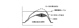
- FIG. 10 is a diagram of an R signal for explaining the reason why the luminance decreases in the highlight portion. It is a figure of G signal for demonstrating the reason a brightness
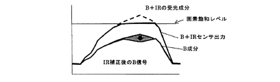
- FIG. 10 is a diagram of an R signal for explaining the reason why the luminance decreases in the highlight portion. It is a figure of G signal for demonstrating the reason a brightness
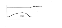
- FIG. 11 is a diagram of an IR signal for explaining the reason why the luminance decreases in the highlight portion. It is a figure which shows the clip level corresponding to each RGB color signal of IR signal.
- FIG. 6 is a diagram for explaining subtraction of clipped IR signals from RGB color signals, where (a) shows the case of the R signal, (b) shows the case of the G signal, and (c ) Is a diagram showing a case of a B signal.
- FIG. 6 is a diagram for explaining white balance processing, where (a) shows a region set to white in the plane of the RY signal and BY signal, and (b) shows white. It is a figure which shows the range of a luminance level.
- FIG. 6 is a diagram for explaining subtraction of clipped IR signals from RGB color signals, where (a) shows the case of the R signal, (b) shows the case of the G signal, and (c ) Is a diagram showing a case of a B signal.
- FIG. 6 is a diagram
- FIG. 6 is a diagram for explaining a method for adjusting the output level of each RGB signal clip after the IR signal is subtracted;
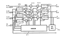
- FIG. 2 is a block diagram illustrating a signal processing unit of the imaging processing apparatus. It is a block diagram which shows the signal processing part as another example same as the above. It is a figure for demonstrating the saturation level of the RGBC color filter of the 7th Embodiment of this invention. It is a figure for demonstrating that the signal level of IR signal calculated
- FIG. 6 is an RGBC signal diagram for explaining the reason why the brightness decreases in the highlight portion. It is a block diagram for demonstrating a separation device equally. It is a block diagram for demonstrating a clip level calculation device same as the above.
- FIG. 2 is a block diagram for explaining an IR signal generation device.
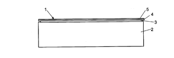
- An image sensor (image sensor) 1 includes, for example, as shown in FIG. 1, a sensor body 2 that is a CCD (Charge Coupled Device) image sensor, and red (corresponding to each pixel of the sensor body 2). R), green (G), blue (B), infrared (IR) regions (filters of each color) arranged in a predetermined arrangement, and a cover glass covering the sensor body 2 and the color filter 3 4 and a DBPF (double band pass filter) 5 formed on the cover glass 4.
- CCD Charge Coupled Device
- the sensor body 2 is a CCD image sensor, and a photodiode as a light receiving element is arranged in each pixel.
- the sensor body 2 may be a CMOS (Complementary Metal Oxide Semiconductor) image sensor instead of the CCD image sensor.
- CMOS Complementary Metal Oxide Semiconductor
- the sensor body 2 is provided with a color filter 3.
- the color filter 3 is obtained by adding an IR filter to the color filter 3x having three filter parts of R, G, and B arranged in each pixel in the general Bayer arrangement shown in FIG. Yes.
- the basic pattern is composed of 16 color filter sections of 4 rows (horizontal arrangement) ⁇ 4 columns (vertical arrangement).
- the first row is F11, F12, F13, F14
- the second row is F21, F22, F23, F24
- the third row is F31, F32, F33, F34
- the eyes are F41, F42, F43, and F44.
- the Bayer array eight filter units F12, F14, F21, F23, F32, F34, F41, and F43 are G, and four filter units F11, F13, F31, and F33 are R, and F22, Four filter parts F24, F42, and F44 are designated as B.
- the reason why the number of G filter units is twice the number of R and B filter units is based on the fact that human eyes are highly sensitive to green. In addition, even if the lower sensitivity is set to high resolution, it may not be recognized by the human eye, but if the higher sensitivity is set to high resolution, it is more likely to be recognized by the human eye. Be recognized.
- the G filters are arranged in a checkered pattern every other row in the row direction (horizontal direction) and in the column direction (vertical direction). The filter parts are arranged without being adjacent to each other.
- the color filter 3 according to the present embodiment has four Rs by setting four of the eight G filter units in the Bayer array as IR.
- G, 4 B, and 4 IR filters 3 a are included. That is, in the basic arrangement of 4 rows and 4 columns, four types of R, G, B, and IR filter units are arranged four by four, and the same type of filter units are adjacent to each other in the row direction and the column direction.
- the R, G, B, and IR filter units are arranged one by one in each column, and two types of filters of the R, G, B, and IR filter units are arranged every other row. Two parts are arranged respectively.
- filter units F11, F13, F32, and F34 are R
- filter units F12, F14, F31, and F33 are IR
- filter units F21, F23, F42, and F44 are used.
- the number of filter sections is G
- the four filter sections F32, F34, F41, and F42 are B.
- the reduction of the G filter unit may cause the resolution to appear to the human eye to be deteriorated, but each color including IR is evenly arranged to facilitate the interpolation (interpolation) process. . Further, the positions of the respective colors are arranged so as to be shifted by one column in the first, second and third and fourth lines. In other words, the color arrangement is reversed left and right in the first, second and third and fourth lines.
- each color is arranged in each column and two colors are arranged in every other row, so the horizontal direction (horizontal direction) rather than the vertical direction (vertical direction).
- the resolution in the horizontal direction due to the IR filter portion can be suppressed.
- the color filter 3a includes a color filter 3a shown in FIG. 5B that is horizontally reversed, vertically inverted, and 180-degree rotated.
- times may be included. However, those rotated 90 degrees and 270 degrees have higher resolution in the vertical direction than in the horizontal direction.
- color filter 3 As in the color filter 3 b shown in FIG. 5C, 2 of the four Bs of the pattern of the color filter 3 x in the Bayer array described above without reducing G that is highly sensitive to humans.
- One may be IR.
- This color filter 3b has a basic arrangement of 4 rows and 4 columns, 8 filter units for G, 4 filter units for R, and B filter among 4 types of filter units of R, G, B, and IR. And two IR filter units are arranged, and the same type of filter units are arranged so as not to be adjacent to each other in the row direction and the column direction.
- the color filter 3b includes a color filter 3b shown in FIG. 5C that is horizontally reversed, vertically inverted, and 180-degree rotated. Moreover, what rotated 90 degree
- the color filter 3c has a basic arrangement of 4 rows and 4 columns, including 8 G filter units, 4 IR filter units, and 4 R filter units of R, G, B, and IR. Two filter units and two B filter units are arranged, and the same type of filter units are arranged so as not to be adjacent to each other in the row direction and the column direction.
- the color filter 3c includes a color filter 3b shown in FIG. 5D that is inverted horizontally, vertically inverted, and rotated 180 times. Moreover, what rotated 90 degree
- a well-known filter can be used for each of the R filter portion, the G filter portion, and the B filter portion of the color filter 3.
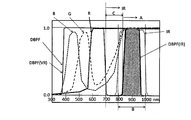
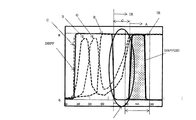
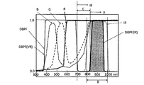
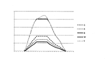
- the transmittance spectra of the R filter unit, the G filter unit, and the B filter unit in the present embodiment are as shown in the graphs of FIGS. 2, 3, and 4. 2, 3 and 4 show the transmittance spectra of the red (R), green (G), blue (B), and infrared (IR) filters of the color filter 3, and the vertical axis. Indicates the transmittance, and the horizontal axis indicates the wavelength.
- the wavelength range in the graph includes a part of the visible light band and the near-infrared band, and indicates a wavelength range of 300 nm to 1100 nm, for example.
- the R filter portion has a substantially maximum transmittance at a wavelength of 600 nm, and the long wavelength side has a substantially maximum transmittance even when the wavelength exceeds 1000 nm. It will be maintained.
- the G filter portion has a peak at which the transmittance is maximized at a portion where the wavelength is about 540 nm, as indicated by G (broken line having a wide interval) in the graph, and the transmittance at a portion where the wavelength is about 620 nm on the long wavelength side. There is a part that becomes minimal. Further, the G filter portion tends to rise on the longer wavelength side from the portion where the transmittance is minimized, and the transmittance is substantially maximum at about 850 nm. On the longer wavelength side, the transmittance is substantially maximum even when the wavelength exceeds 1000 nm.
- the filter part of B has a peak where the transmittance is maximized at a part where the wavelength is about 460 nm, as shown in B (dashed broken line) of the graph, and a part of about 630 nm on the long wavelength side thereof, There is a part where the transmittance is minimized. Further, the longer wavelength side tends to increase, and the transmittance is substantially maximized at about 860 nm. On the longer wavelength side, the transmittance is substantially maximized even if it exceeds 1000 nm.
- the IR filter portion blocks light on the short wavelength side from about 780 nm, blocks light on the long wavelength side from about 1020 nm, and the portion of about 820 nm to 920 nm has a substantially maximum transmittance.
- each of the R, G, B, and IR filter units is not limited to that shown in FIG. 2 and the like, but the color filter 3 that is currently used generally has a transmittance close to this. It seems to show a spectrum.
- 1 on the horizontal axis indicating the transmittance does not mean that 100% of light is transmitted, but the color filter 3 indicates, for example, the maximum transmittance.
- the cover glass 4 covers and protects the sensor body 2 and the color filter 3.
- the DBPF 5 is an optical filter formed on the cover glass 4.
- the DBPF 5 has a transmission characteristic in the visible light band, a cutoff characteristic in the first wavelength band adjacent to the long wavelength side of the visible light band, and a second wavelength that is a part of the first wavelength band.
- An optical filter having transmission characteristics in a band.
- the DBPF 5 is located at a position slightly apart from the visible light band indicated by DBPF (VR) on the long wavelength side with respect to the visible light band, as indicated by DBPF (solid line) in the graph.
- the transmittance of the two bands of the infrared band (second wavelength band) indicated by DBPF (IR) is high.
- DBPF (VR) as a band having a high transmittance in the visible light band has a wavelength band of about 370 nm to 700 nm, for example.
- DBPF (IR) as the second wavelength band having high transmittance on the infrared side is, for example, a band of about 830 nm to 970 nm.
- the relationship between the transmittance spectrum of each filter section of the color filter 3 and the transmittance spectrum of DBPF 5 is defined as follows. That is, DBPF (IR), which is the second wavelength band that transmits infrared light in the transmittance spectrum of DBPF5, has the maximum transmittance of the cheek at all of the R filter unit, the G filter unit, and the B filter unit. 2 is included in the wavelength band A shown in FIG. 2 where the transmittance is substantially the same in each filter unit, and is also included in the wavelength band B that transmits light at the substantially maximum transmittance of the IR filter unit. It has become.
- DBPF IR
- the wavelength band A in which the transmittances of the R, G, and B filter portions are substantially the same is a portion where the transmittance difference of each filter portion is 10% or less.
- the transmittances of the G and B filter units are lower than the R filter unit having the maximum transmittance.
- DBPF5 the difference in transmittance of the R, G, and B filter portions is DBPF (VR), which is a portion with high transmittance in the visible light band, and the second wavelength band in the infrared light band. This corresponds to a portion where the transmittance for substantially blocking the light of DBPF 5 between DBPF (IR) and the portion having a high transmittance is minimal.
- the transmission of light in a portion where the difference in transmittance between the R, G, and B filter portions becomes large is cut, and the transmittance of each filter portion becomes substantially maximum on the longer wavelength side.
- Light is transmitted in the wavelength band A where the transmittance is substantially the same.
- DBPF 5 used in place of the infrared light cut filter has a region that transmits light not only in the visible light band but also in the second wavelength band on the infrared light side. Therefore, in color imaging with visible light, it is affected by the light that has passed through the second wavelength band.
- the second wavelength band has transmittance in each of the R, G, and B filter units. The light of different portions is not transmitted, and only the light in the wavelength band in which the transmittance of each filter unit is substantially maximized and has substantially the same transmittance is transmitted.
- the R filter unit is used in the second wavelength band.
- G filter part, B filter part, IR filter part light passes through in substantially the same manner, and as infrared light, light of substantially the same amount of light in each filter part including IR is image sensor body To the photodiode of the above-mentioned pixel.
- the amount of light that passes through the second wavelength band on the infrared side of the light that passes through the R, G, and B filters is the same as the amount of light that passes through the IR filter section.
- the output signal of the assumed pixel from the sensor body 2 receiving the light transmitted through the R, G, and B filters and the IR filter as described above are passed.
- R, G, and B obtained by cutting off the infrared light that has passed through the R, G, and B filter sections as the difference from the assumed pixel output signal from the sensor body 2 that has received the light as described above.
- the output signal of the visible light portion is the output signal of the visible light portion.
- each pattern of the color filter 3 (3a, 3b, 3c)
- one of the R, G, B, and IR filter sections is arranged in each pixel of the sensor body 2. Therefore, there is a high possibility that the amount of light of each color irradiated to each pixel is different.
- interpolation method for each color of each pixel Luminance is obtained, and the difference between the interpolated R, G, and B luminances of the interpolated pixels and the interpolated IR luminance can be set as the R, G, and B luminances, respectively.
- the image processing method for removing the infrared light component from the luminance of each color of R, G, B is not limited to this, and finally passes through the second wavelength band from each luminance of R, G, B. Any method may be used as long as it can cut the influence of light.
- the DBPF 5 cuts a portion where the transmittance of the R, G, B filter portion on the infrared side is different from 10%, that is, a portion where the transmittance is different from a predetermined ratio. This makes it easy to remove the influence of infrared light.
- the use of the image sensor 1 is to use it as an image sensor in an image pickup apparatus capable of both color photographing and infrared light photographing.
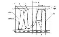
- the transmittance spectrum of DBPF 5 shown in FIG. 3 takes into account the transmittance spectrum of each of the R, G, B, and IR filter sections and the emission spectrum of light for infrared illumination, for example, the infrared LED for illumination. Determined. 3, in addition to the transmittance spectra R, G, B, IR of the filter units of the same colors as in FIG. 2 and the transmittance spectrum DBPF of DBPF 5, the emission spectrum IR-light of LED illumination is shown.
- the second wavelength band indicated by DBPF (IR) which is a part that transmits infrared light of the DBPF shown in FIG. 3, is an R filter unit, a G filter unit, and a B filter. 2 are included in the wavelength band A shown in FIG. 2 where the transmittance is substantially the same in each filter portion, and light is transmitted with the maximum transmittance of the IR filter portion.
- the wavelength band B to be included.
- substantially the entire wavelength band that is the peak of the emission spectrum of infrared illumination included in both the wavelength band A and the wavelength band B described above is included in the DBPF (IR) wavelength band.
- the second wavelength band indicated by DBPF (IR) does not have to be wider than the peak width of the optical spectrum of infrared light illumination when infrared light photography is performed under infrared light illumination instead of nighttime natural light.
- the peak width of the emission spectrum of the infrared light illumination is approximately the same as the peak width having a peak at about 860, for example. You may provide the peak part of the transmittance
- the peak in the emission spectrum of infrared illumination indicated by IR-light is on the short wavelength side of the above-described wavelength band A and wavelength band B, and the second wavelength of DBPF indicated by DBPF (IR)
- the band substantially overlaps the peak of the emission spectrum in the IR-light of the short wavelength side portion of the wavelength band A and the wavelength band B.
- the graph shown in FIG. 4 is similar to the fluff shown in FIG. 3 in that the emission spectrum of infrared illumination is added to the graph shown in FIG. 2 and the infrared side transmittance of the DBPF5 transmittance spectrum is high.
- the second wavelength band indicated by a certain DBPF (IR) is adjusted to the peak of the emission spectrum indicated by IR-light of the above-mentioned infrared illumination.
- infrared light illumination having a longer emission spectrum peak wavelength than that shown in FIG. 3 is used, and this peak is included in the above-described wavelength band A and wavelength band B. It exists on the long wavelength side of the wavelength band A and the wavelength band B.
- the second wavelength band indicated by DBPF (IR) of DBPF 5 is provided so as to be substantially umbrella with the peak indicated by IR-light of infrared illumination in the above-mentioned wavelength band A and wavelength band B. .
- the second wavelength band of DBPF 5 may be that shown in any of FIGS. 2, 3, and 4, and the second wavelength band is included in both wavelength band A and wavelength band B described above. It only has to be done. Further, when the wavelength band that is the peak of the emission spectrum of infrared light illumination used for nighttime infrared light photography is determined, the wavelength band is included in both the wavelength band A and the wavelength band B described above. In addition, it is preferable to match the second wavelength band of DBPF 5 with the peak of the emission spectrum of infrared illumination.
- the second wavelength band that transmits light on the infrared side of the DBPF 5 is the infrared side of each of the R, G, B, and IR filter units, and the transmittance of each filter unit is substantially the same.
- the maximum is included in the wavelength band A when the transmittance of each filter part is substantially the same, and is included in the wavelength band B where the transmittance of the IR filter part is substantially maximum.
- the transmittance of each of the R, G, and B filters is substantially maximum only for the R fill portion, and the transmittance of the G and B filter portions is substantially maximum. Due to the absence, the transmittances of the R, G, and B filter portions are not substantially the same, and different portions of light are cut by the DBPF 5.
- each filter part of R, G, B, IR since the light of the second wavelength band is transmitted on the infrared side, the infrared side transmittance in each filter part is substantially the same, If the light in the second wavelength band is irradiated with the same light amount, the transmitted light amounts in the R, G, B, and IR filter units are the same. Thereby, as described above, the color based on the output signal from the pixel corresponding to each of the R, G, and B filter units is corrected, and the influence of the infrared light passing through the second wavelength band of the color at the time of color photographing is performed. It is possible to easily obtain an image in which the above is suppressed.
- the second wavelength band corresponds to the peak of the emission spectrum of the infrared light illumination included in the wavelength band A and the wavelength band B described above, the light of the infrared light illumination can be used efficiently,
- the width of the second wavelength band can be narrowed to reduce the influence of infrared light passing through the second wavelength band during color photography.
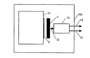
- FIG. 6 shows an imaging apparatus 10 using the imaging sensor 1 of the present embodiment.
- the imaging device 10 processes the imaging lens 11, the imaging sensor 1 including the DBPF 5, and the output signal 13 output from the imaging sensor 1, and performs the above-described interior processing or the second wavelength during color imaging.
- a signal processing unit (signal processing device) 12 that performs image processing for removing the influence of infrared light that has passed through the band, image processing such as gamma correction, white balance, and RGB matrix correction on the image signal is provided.
- a visible color image output signal 14 and an infrared light image output signal 15 can be output from the image processing unit.
- the lens 11 constitutes an optical system that connects an image on the image sensor 1 of the image pickup apparatus 10.
- the lens 11 is composed of a plurality of lenses, for example.
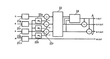
- FIG. 7 is a block diagram showing signal processing in the signal processing unit 12 of the imaging apparatus 10. Output signals from the R, G, B, and IR pixels are sent to the interior processing blocks 21r, 21g, 21b, and 21ir. In each of the interior processing blocks 21r, 21g, 21b, and 21ir, for example, as shown in FIG.
- the infrared light removal signal creation blocks 22r, 22g, 22b, and 22ir in order to remove the influence of the infrared light received from the second wavelength band described above, signals of each color of R, G, and B are used. A signal to be subtracted from is generated from the IR signal.
- the signals created for each of R, G, and B by the infrared light removal signal creation blocks 22r, 22g, and 22b are subtracted from the signals of the R, G, and B colors.
- the IR signal is basically removed from the R, G, and B signals, which facilitates processing.
- the sensitivity differs for each color pixel depending on the characteristics of the filter section of each pixel, and therefore, a signal to be subtracted from each R, G, B signal for each R, G, B image from the IR signal. create.
- the R, G, and B signals are converted into R, G, and B signals using a determinant to correct the colors, and a known RGB matrix process is performed.
- the well-known gamma correction which is the correction for the image output to a known white balance process and a display etc. which makes the output value of each signal of R, G, B become the same is performed.
- a signal of luminance Y is generated by multiplying the R, G, B color signals by coefficients. Also, by dividing the luminance Y signal from the blue B signal and the red R signal, the RY and BY color difference signals are calculated, and Y, RY, and BY signals are output. To do.
- the IR signal is basically output as a monochrome gradation image.
- such an imaging apparatus 10 as described in the above-described imaging sensor 1, it is possible to easily perform image processing for removing the influence of infrared light from a color image, and a visible color image having excellent color reproducibility. Can be obtained. In addition, the development cost of such an imaging apparatus can be reduced.
- the R, G, and B filter units have mutually different transmittances. Since it is physically cut by the DBPF, in the image processing, it is only necessary to perform a process of cutting the IR light at a portion where the transmittance is substantially maximum on the infrared side of each of the R, G, and B filter portions. It will be. In this case, image processing becomes easy, and it becomes possible to obtain color image data having the same color reproducibility as when a conventional infrared light cut filter is used.
- the light that passes through the R, G, and B filter sections and reaches the photodiode is the same as the visible light that has passed through the respective filter sections in the visible light region and the R, G, and B filter sections.
- the infrared light that has passed through the second wavelength band that is the same in the IR filter section. Therefore, for example, the output signal of the IR after the interpolation processing corrected according to the characteristics such as the sensitivity based on the filter unit of each color is subtracted from each output signal after the interpolation processing of the R, G, B of the imaging sensor 1. By doing this, it is possible to obtain color reproducibility close to that when an infrared cut filter is used.
- each filter unit substantially It is difficult to obtain the amount of infrared light that should be cut from the light that has passed through the image, and it is difficult to obtain image data having the same color reproducibility by using image processing as when an infrared light cut filter is used. .
- the image pickup apparatus 10 a is such that the image sensor 1 is not provided with the DBPF 5 but the lens 11 is provided with DPBF.
- the imaging device 10a processes the imaging lens 11 provided with the DBPF 5, the imaging sensor 1, and the output signal 13 output from the imaging sensor 1, and performs the above-described interior processing and the second wavelength during color imaging.
- a signal processing unit 12 that performs image processing for removing the influence of infrared light that has passed through the band, image processing such as gamma correction, white balance, and RGB matrix correction on the image signal.
- a visible color image output signal 14 and an infrared light image output signal 15 can be output from the image processing unit.
- the DBPF 5 and the color filter 3 are the same as the DBPF 5 and the color filter 3 of the first embodiment.
- the transmittance of each of the R, G, B, and IR filter portions of the color filter 3 and the second of the DPBF 5 The relationship of the wavelength band DBPF (IR) is the same as that of the first embodiment. Therefore, unlike the first embodiment, even if the lens 11 is provided with the DBPF 5, the same operational effects as those of the imaging device 10 of the first embodiment can be obtained.
- the DBPF 5 is provided in the optical system of the imaging device 10a, and has a visible light band (DBPF (VR)) and a second wavelength band on the infrared side (DBPF (IR)) with respect to light reaching the imaging sensor 1. So that the light is blocked at the short wavelength side of the visible light band, the long wavelength side of the second wavelength band, and the wavelength band between the visible light band and the second wavelength band. It may be provided anywhere as long as it is.
- the imaging sensor 1 and the imaging apparatus according to the third embodiment are different in the configuration of a part of the color filter 3 and the IR component removal method from the RGB signals.
- the color filter 3 and the IR component removal method will be described below.
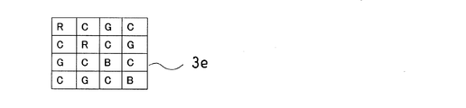
- the color filter 3e (RGBC configuration 1), for example, as shown in FIG. 10, two of the four B of the pattern of the color filter 3x in the Bayer array described above are represented as C. Two of the two R's are C, and four of the eight G's are C. That is, the color filter 3e has a basic arrangement of 4 rows and 4 columns, of 4 types of R, G, B, and C filter units, 4 G filter units, 8 C filter units, Two filter units and two B filter units are arranged, and the same type of filter units are arranged so as not to be adjacent to each other in the row direction and the column direction. Accordingly, the eight C filter units are arranged in a checkered pattern.
- C indicates a transparent state as a clear filter part, and basically has transmission characteristics from the visible light band to the near-infrared wavelength band.
- the visible light band C R + G + B.
- the R, G, and B filter sections have transmission characteristics on the long wavelength side of the visible light band. Even in the C filter section, which is a clear filter section, light is transmitted on the long wavelength side of the visible light band.
- the infrared that transmits the longer wavelength side than the visible light band is limited to the second wavelength band, and R
- the amount of light passing through the G, B, and C filter units and the DBPF 5 is almost the same (approximate) in each of the R, G, B, and C filter units, and in the visible light band, the R, G, B, and C filters
- the transmission characteristics differ according to the wavelength of the part.
- the infrared that transmits longer wavelengths than the visible light band is limited to the second wavelength band, and R, G, B, IR
- the amount of light passing through the filter unit and the DBPF 5 is substantially the same in each of the R, G, B, and IR filter units, and in the visible light band, transmission characteristics corresponding to the wavelengths of the R, G, B, and IR filter units are provided. Different.
- the third embodiment it is possible to perform IR correction of each pixel with high accuracy and to generate a visible image with high color reproducibility.
- it does not include the above-described IR filter unit that has a cutoff characteristic in substantially the entire wavelength range of the visible light band and has a transmission characteristic in the infrared on a longer wavelength side than the visible light band.
- the C filter unit the IR signal can be calculated by the following equation.
- C (W), R, G, B, and IR indicate the level of the output signal from the imaging sensor 1, but C (W), R, G, and B indicate the level of the visible light band. It is assumed that the infrared component is not included.
- IR represents an actual value obtained by measurement or the like
- IR ′ represents a value obtained by calculation.
- the IR transmittance of each filter unit can be approximated by the DBPF 5, and the IR component is obtained as described above. By removing this from the signal of each filter unit, color reproducibility can be improved.
- the amount of light received by the pixel is likely to be saturated and the C filter section reduces the amount of light received in the visible light band, and the infrared wavelength band and visible light band.
- the amount of received light may be lowered over a wavelength band including the above, or the charge accumulated with respect to the amount of received light may be reduced in the element portion constituting the pixel in each pixel. In that case, it is necessary to change the above formula accordingly.
- FIG. 12 shows another arrangement of R, G, B, and C color filters.
- R, G, B, and C are evenly arranged one by one. is there.
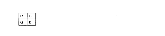
- R, G, B Bayer array as shown in FIG. 13
- R and B are arranged one by one and two G are arranged.
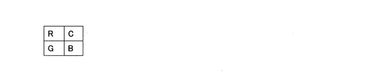
- a 2 ⁇ 2 array of R, G, B, and IR color filters in which one of the conventional arrays that does not include C or IR is changed to IR is, as shown in FIG. G, B, and IR are arranged one by one.
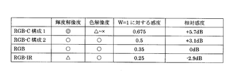
- the RGB-C configuration 1 shown in FIG. 10 the RGB-C configuration 2 shown in FIG. 12, the conventional RGB array (Bayer array) shown in FIG. 13, and the RGB-IR array shown in FIG.
- the RGB-C (Configuration 1) sensor has a high luminance resolution due to the checkered arrangement of C, but RGB pixels are sparse,
- the resolution is low and moire tends to occur.
- the resolution required for the color signal is lower than that of the luminance signal, which is 1/2 or less, so that there is no problem.
- the sensitivity is high.
- RGB-C (Configuration 2) has the same luminance resolution and color resolution as the conventional RGB sensor, and has higher sensitivity than the RGB sensor.
- the RGB-IR sensor is provided with an IR that does not have transmission characteristics in the visible light band, so that the sensitivity is lower than that of the RGB sensor, and the luminance resolution is also lower. That is, the color filter having C is more likely to be advantageous in resolution and sensitivity than the color filter having IR of the first embodiment and the second embodiment.
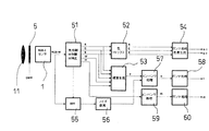
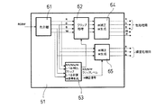
- FIG. 16 is a block diagram showing signal processing in the signal processing unit 12 of FIG.
- the imaging sensor 1 includes the RGB-C sensor 1 including the above-described RGB-C color filter 3e, and also includes a lens 11 and a DBPF 5 that constitute an optical system.
- R + IR, G + IR, B + IR, and C + IR signals are input from the RGB-C sensor 1 to a separation device 51 that performs color separation, IR separation, and IR correction, and R, G, B, W, and IR signals are obtained and output. This process is performed based on the calculation using the above-described equation.
- R, G, B, W, and IR signals output from the separation device 51 R, G, and B signals are sent to the color matrix device 52, where known RGB matrix correction and the like are performed, and RGB signals. Is output. Also.
- the R, G, B, W, and IR signals from the separation device 51 are sent to the luminance generation device 53, and a luminance signal is generated from each signal based on an equation for obtaining the set luminance.
- the RGB signal output from the color matrix device is input to the gamma processing and color difference generation device 54, where known gamma processing is performed, and for example, BY and RY signals are generated as the color difference signals.
- the signals output from the separation device 51 and the RGB-C sensor 1 are reduced in noise after being reduced in noise by a noise reduction device 56 as a signal in a predetermined wavelength band via a BPF (band pass filter) 55.
- the signal is amplified by the enhancement processing device 57 together with the luminance signal output from the generation device 53, and is output as a luminance signal (Y signal) of the luminance / chrominance signal through the gamma processing in the gamma processing device 58.
- the IR signal output from the separation device 51 is output as an IR signal via the enhancement processing device 59 and the gamma processing device 60. In the image signal processing, clip processing described later is performed, and the clip processing will be described later.
- the fourth embodiment is a generalization of each color of the color filter, and shows that the color filter of the present invention is not limited to RGB-IR or RGB-C.
- a method for removing an IR component in an imaging sensor including a color filter having a generalized four-color filter unit will be described.
- the four color (four types) filter units basically have different transmission characteristics according to the wavelength in the visible light band, and the wavelength band including the second wavelength band of the DBPF described above includes a visible light band.
- a third wavelength band having a transmittance difference of 10% or less with other filter units on the longer wavelength side is provided, and the third wavelength band includes the second wavelength band of DBPF5. ing.
- IR can be separated by designing a color filter under the following conditions in a filter arrangement of four types of pixels.
- the filter arrangement is preferably a 2 ⁇ 2 arrangement, and each of the four types of filter sections A, B, C, and D is provided.
- A, B, C, and D indicate the level of the output signal from the imaging sensor 1 in the visible light band of each filter unit.
- the IR transmittance is substantially constant in the above-described third wavelength bands of the A, B, C, and D filter units.
- the IR transmittance may be approximately an integral multiple of a certain IR transmittance in each of the A, B, C, and D filter units.
- IR transmittance is constant as described above
- IR ′ (Ka (A + IR) + Kb (B + IR) + Kc (C + IR) + Kd (D + IR)) / (Ka + Kb + Kc + Kd)
- C ′ C + IR ⁇ (Ka (A + IR) + Kb (B + IR) + Kc (C + IR) + Kd (D + IR)) / (Ka + Kb + Kc +
- a ' A + IR * KIRa-KIRa (Ka (A + IR * KIRa) + Kb (B + IR * KIRb) + Kc (C + IR * KIRc) + Kd (D + IR * KIRd)) / (Ka * KIRa + Kb * KIRb + Kc * KIRc + Kd * KIRd)
- B ' B + IR * KIRb-KIRb (Ka (A + IR * KIRa) + Kb (B + IR * KIRb) + Kc (C + IR * KIRc) + Kd (D + IR * KIRd)) / (Ka * KIRa + Kb * KIRb + Kc * KIRc + Kd * KIRd)
- C ' C + IR * KIRc-KIRc (Ka (A + IR * KIRa) + Kb (B + IR * KIRb) + Kc (C + IR * KIRc) + Kd (D + IR * KIRd)) / (Ka * KIRa + Kb * KIRb + Kc * KIRc + Kd * KIRd)
- D ' D + IR * KIRd-KIRd (Ka (A + IR * KIRa) + Kb (B + IR * KIRb) + Kc (C + IR * KIRc) + Kd (D + IR * KIRd)) / (Ka * KIRa + Kb * KIRb + Kc * KIRc + Kd * KIRd)
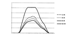
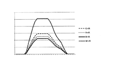
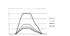
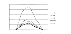
- each filter unit The spectral transmission characteristics of each filter when using DBPF are as shown in FIG.
- the filter unit four types of filter units of R + IR, G + IR, B + IR, and C + IR are used.
- the IR portion is constant or an integer multiple of each other, so that KaA + KbB + KcC + KdD ⁇ 0.
- each filter unit is not limited to R + IR, G + IR, B + IR, and C + IR.
- FIG. 18 shows spectral transmission combining the B filter unit and DBPF5
- FIG. 19 shows spectral transmission combining the G filter unit and DBPF5
- FIG. 20 shows spectral transmission combining the B filter unit and DBPF5.
- FIG. 21 shows the spectral transmission obtained by combining the C (W) filter unit and the DBPF 5.
- Each spectral transmission characteristic is obtained by adding four transmittances of a visible R transmission region, a visible G transmission region, a visible B transmission region, and an IR transmission region, as shown in the above-described equations. . From this, the signal values of each visible R transmission region, visible G transmission region, visible B transmission region, and IR transmission region can be calculated from the values of four or more types of filters. The spectral transmission characteristics are determined based on the above-described equations indicating the branch transmission characteristics of B, C, and D. Six types are determined from combinations of spectral transmission characteristics of two of these filters.
- the imaging sensor 1 that outputs a signal in the visible light band and an infrared signal on the longer wavelength side is mounted on a smartphone or the like, on the smartphone side, a circuit that processes a signal from the imaging sensor 1 is a main circuit.
- the signal is on an SOC (System On Chip) functioning as an arithmetic processing unit
- the RGB signal output from the image sensor includes an IR component as described above, and processing that removes the IR component is required.
- the smartphone needs to be provided with a circuit for performing the IR correction described above. In these cases, when an imaging sensor capable of outputting both visible light and infrared image signals is introduced into a device such as a smartphone, an increase in cost occurs in a portion other than the imaging sensor.
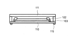
- the imaging sensor 101 includes an imaging unit 102 and an IR correction / separation circuit 103 having substantially the same configuration as the above-described imaging sensor 1.
- a visible RGB signal and an IR signal are output.
- the IR correction / separation circuit 103 includes a circuit that performs processing related to clipping of a signal level described later.
- the RGB signal and the IR signal are output, the number of pins of the image sensor 101 increases.
- the increase in the number of pins can be suppressed by outputting with a serial output standard such as CSI-2.
- the visible RGB signal is output as a RAW signal output of a RGBG Bayer array image sensor or a YUYV (YCb, YCr) signal.
- the IR signal by outputting the IR signal as a single color signal, simultaneous imaging of visible and near infrared can be utilized by the RGB-IR sensor and the RGB-C sensor without changing the SOC of the smartphone or the future phone.
- the structure of the image sensor 101 is, for example, a stacked stack structure as shown in FIG. 23.
- an integrated circuit chip constituting the IR correction / separation circuit 103 is mounted on one substrate 110, and A chip that constitutes the imaging unit 102 is placed over the top.
- a cover glass 111 is disposed on the imaging unit 102.
- Solder balls 115 are disposed on the bottom surface of the substrate 110.
- the structure of the image sensor 101 is such that two substrates 110 are stacked one above the other at an interval in the vertical direction, and the chip of the IR correction / separation circuit 103 is placed on the lower substrate 110.
- the chip of the imaging unit 102 may be arranged on the upper substrate 110, and the cover glass 111 may be arranged thereon.
- the IR correction / separation circuit 103 and the imaging unit 102 can be stacked one above the other as described above to form a single package sensor. Even with this method, the image sensor 101 incorporating the IR correction / separation circuit can be realized with a single package. In this manner, a small sensor that can simultaneously capture small visible / near infrared light and can be used in a smartphone or the like can be realized without including a correction separation circuit.
- a smartphone has functions such as biometric authentication such as iris authentication and 3D capture using an IR sensor, and can capture a moving image / still image with a single sensor.
- FIG. 25 shows a schematic diagram of signal output similar to the RGB Bayer arrangement by IR correction + interpolation.
- R / IR and G / B are output line-sequentially with R, IR, R, IR,... / G, B, G, B,.
- IR correction / IR separation is performed, and the position of the IR pixel is interpolated from the neighboring G signal to generate a G ′ signal, and R, G ′, R, G ′,... / G, B , G, B,..., And outputs visible R / G ′ and G / B signals and separated IR signals.
- the signal processing side can perform processing using the same signal processing circuit.
- the signal processing unit can also perform processing by normal monochrome signal processing.
- the RGB-IR sensor has been described. Even in the visible / near-infrared simultaneous imaging using the RGB-C sensor, an IR correction / separation circuit is incorporated in the sensor, and a conventional RGB Bayer array is incorporated. A similar effect can be obtained by configuring the sensor output format to output a visible signal and an IR signal.
- the imaging apparatus 10 processes a lens 11 that is an optical system for photographing, an imaging sensor 1 that includes a DBPF 5, and an output signal 13 that is output from the imaging sensor 1.
- the image processing includes image processing such as the above-described interior processing, image processing that removes the influence of infrared light that has passed through the second wavelength band during color shooting, gamma correction, white balance, and RGB matrix correction.
- a signal processing unit signal processing device: subtraction control device
- the signal processing unit 12 can output a visible color image output signal 14 (visible image signal) and an infrared light image output signal 15 (infrared image signal).
- the lens 11 constitutes an optical system that connects an image on the image sensor 1 of the image pickup apparatus 10.
- the lens 11 is composed of a plurality of lenses, for example.
- the imaging sensor (image sensor) 1 includes a sensor body 2 that is a CCD (Charge Coupled Device) image sensor, and red (R) and green (corresponding to each pixel of the sensor body 2). G), blue (B), infrared (IR) regions (filters of each color) arranged in a predetermined arrangement, a color filter 3, a cover glass 4 covering the sensor body 2 and the color filter 3, and a cover glass 4 and a DBPF (double band pass filter) 5 formed on the substrate 4.
- CCD Charge Coupled Device
- the sensor body 2 is a CCD image sensor, and a photodiode as a light receiving element is arranged in each pixel.
- the sensor body 2 may be a CMOS (Complementary Metal Oxide Semiconductor) image sensor instead of the CCD image sensor.
- CMOS Complementary Metal Oxide Semiconductor
- the sensor body 2 is provided with a color filter 3.
- a Bayer array color filter that has red R, green G, and blue B regions but no infrared IR region has 16 regions of 4 ⁇ 4 in length, which is a basic pattern. Each region is a G region, four regions are R, and four regions are B.
- the color filter 3 of the present embodiment four of the eight G regions in the Bayer array are IR regions, so that four Rs are obtained.
- G is 4
- B is 4
- IR is 4.
- the color filter including the IR region is not limited to the color filter 3 illustrated in FIG. 28, and various color filters can be used.
- Each of the RGB regions is a general RGB filter, but has a transmittance peak in the wavelength range of each color and transparency in the near-infrared wavelength region.
- the R region was R + IR
- the green region was G + IR
- the blue region was B + IR.
- the transmittance spectrum of the R region, the G region, and the B region in the present embodiment is as shown in the graph of FIG. That is, the transmittance spectrum of each of the red (R), green (G), blue (B), and infrared (IR) filters of the color filter 3 is shown, the vertical axis indicates the transmittance, and the horizontal axis indicates the transmittance. It is a wavelength.
- the wavelength range in the graph includes a part of the visible light band and the near-infrared band, and shows a wavelength range of 300 nm to 1100 nm, for example.
- the R region has a substantially maximum transmittance at a wavelength of 600 nm, and the long wavelength side maintains a substantially maximum transmittance even when the wavelength exceeds 1000 nm. It will be in the state.
- the G region has a peak at which the transmittance is maximized at a portion where the wavelength is about 540 nm, as shown by G (broken line having a wide interval) in the graph, and the transmittance is minimized at a portion where the wavelength is about 620 nm. There is a part that becomes.
- the longer wavelength side tends to increase from the portion where the transmittance is minimized, and the transmittance is substantially maximum at about 850 nm.
- the transmittance is substantially maximum even when the wavelength exceeds 1000 nm.
- the region B has a peak at which the transmittance is maximized at a portion where the wavelength is about 460 nm, as shown by B (dashed broken line) in the graph, and is transmitted at a portion around 630 nm on the long wavelength side. There is a part where the rate is minimal. Further, the longer wavelength side tends to increase, and the transmittance is substantially maximized at about 860 nm. On the longer wavelength side, the transmittance is substantially maximized even if it exceeds 1000 nm.
- the IR region blocks light on the short wavelength side from about 780 nm, blocks light on the long wavelength side from about 1020 nm, and the portion of about 820 nm to 920 nm has a substantially maximum transmittance.
- the transmittance spectrum in each of the R, G, B, and IR regions is not limited to that shown in FIG. 29.
- the color filter 3 that is currently used generally has a transmittance spectrum close to this. It seems to show. Note that 1 on the vertical axis indicating the transmittance does not mean that 100% of the light is transmitted, and the color filter 3 indicates, for example, the maximum transmittance.
- the cover glass 4 covers and protects the sensor body 2 and the color filter 3.
- the DBPF 5 is an optical filter formed on the cover glass 4.
- the DBPF 5 has a transmission characteristic in the visible light band, a cutoff characteristic in the first wavelength band adjacent to the long wavelength side of the visible light band, and a second wavelength that is a part of the first wavelength band.
- the arrangement position of the DBPF 5 is not limited to the cover glass 4, and may be arranged at another location of the imaging sensor 1. Further, the arrangement position of the DBPF 5 is not limited to the image sensor 1 and may be arranged in an optical system that includes the lens 11 and forms an image on the image sensor 1.
- the DBPF 5 has a visible light band indicated by DBPF (VR) as shown by a DBPF (solid line) in the graph, and a DBPF at a position slightly distant from the visible light band on the long wavelength side.
- the transmittance of two bands of the infrared band (second wavelength band) indicated by (IR) is high.
- DBPF (VR) as a band having high transmittance in the visible light band has a wavelength band of about 370 nm to 700 nm, for example.
- DBPF (IR) as the second wavelength band having high transmittance on the infrared side is, for example, a band of about 830 nm to 970 nm.
- the relationship between the transmittance spectrum of each region of the color filter 3 and the transmittance spectrum of DBPF 5 is defined as follows. That is, DBPF (IR), which is the second wavelength band that transmits infrared light of the transmittance spectrum of DBPF5, has the cheek maximum transmittance in all of the R region, the G region, and the B region. It is included in the wavelength band A shown in FIG. 29 in which the transmittance is substantially the same in the region, and is also included in the wavelength band B that transmits light with the substantially maximum transmittance in the IR region.
- DBPF IR
- the wavelength band A in which the transmittance in each of the R, G, and B regions is substantially the same is a portion where the transmittance difference in each region is 10% or less.
- the transmittance of the G and B regions is lower than the R region where the transmittance is substantially maximum.
- DBPF5 the portion where the transmittance of each region of R, G, and B is different is DBPF (VR) which is a portion where the transmittance in the visible light band is high, and the second wavelength band in the infrared light band.
- DBPF 5 used in place of the infrared light cut filter has a region that transmits light not only in the visible light band but also in the second wavelength band on the infrared light side. Therefore, in color imaging with visible light, it is affected by light that has passed through the second wavelength band, but the second wavelength band has different transmittances in the R, G, and B regions as described above. A portion of light is not transmitted, and only the light in the wavelength band in which the transmittance of each region is substantially maximized and becomes substantially the same transmittance is transmitted.
- the amount of light that passes through the second wavelength band on the infrared side of the light that passes through the R, G, and B filters is the same as the amount of light that passes through the IR region.
- the output signal of the assumed pixel from the sensor body 2 receiving the light transmitted through the R, G, and B filters and the IR filter as described above are passed.
- the difference from the output signal of the pixel assumed as described above from the sensor main body 2 that has received the light is that of each of R, G, and B obtained by cutting the infrared light that has passed through the R, G, and B regions. It becomes the output signal of the visible light part.
- any one region of R, G, B, IR is arranged for each pixel of the sensor body 2. Since the light quantity of each color light irradiated to each pixel is likely to be different, for example, the brightness of each color of each pixel by using a well-known interpolation method (interpolation method) in each pixel. And the difference between the R, G, and B luminances of each interpolated pixel and the interpolated IR luminance can be set as the R, G, and B luminances, respectively.
- the image processing method for removing the infrared light component from the luminance of each color of R, G, B is not limited to this, and finally passes through the second wavelength band from each luminance of R, G, B. Any method may be used as long as it can cut the influence of light.
- the DBPF 5 cuts a portion where the transmittance of the R, G, B region on the infrared side is different from 10%, that is, a portion where the transmittance is different from a predetermined ratio. Processing that removes the influence of infrared light becomes easy.
- the use of the image sensor 1 is to use it as an image sensor in an image pickup apparatus capable of both color photographing and infrared light photographing.
- the transmittance spectrum of DBPF 5 shown in FIG. 29 takes into account the transmittance spectrum of each region of R, G, B, and IR and the emission spectrum of light for infrared light illumination, for example, the infrared light LED for illumination. decide.
- the second wavelength band that transmits light on the infrared side of the DBPF 5 is the infrared side of each of the R, G, B, and IR regions, and the transmittance of each region is substantially maximum.
- the transmittance of each of the R, G, and B filters is substantially maximum only for the fill portion of R, and the transmittance of the G and B regions is not substantially maximum.
- the transmittances of the R, G, and B regions are not substantially the same, but different portions of light are cut by the DBPF 5.
- the second wavelength band corresponds to the peak of the emission spectrum of the infrared light illumination included in the wavelength band A and the wavelength band B described above, the light of the infrared light illumination can be used efficiently,
- the width of the second wavelength band can be narrowed to reduce the influence of infrared light passing through the second wavelength band during color photography.
- the DBPF 5 it is possible to perform highly accurate correction by subtracting the value of each IR signal from the value of each RGB signal of the imaging sensor 1.
- the signal processing unit 12 an imaging processing method in the imaging apparatus will be described.
- the light receiving components of the pixels of each color of the image sensor 1 are in a state in which an IR component is added to the components of each color as shown below.
- IR correction is performed by removing the IR component from the light receiving components of the RGB pixels excluding the IR pixels.
- the IR component that passes through the DBPF 5 and passes through the color filter can be excluded from each color region other than the IR of the color filter.
- the R pixel, the G pixel, and the B pixel have different sensitivities to each light source, and each pixel of the image sensor 1 has a dynamic range, and charges that exceed the dynamic range cannot be read out.
- the output is clipped and capped. That is, when the input light exceeds the dynamic range, the output signal is clipped and cut off.
- errors occur in the corrected R signal, G signal, and B signal, causing problems such as unnatural luminance level (the luminance of the highlight portion decreases) and coloring in highlights. .
- FIGS. 30 to 32 are diagrams for explaining a problem when the IR component is subtracted from each color component in a state where the dynamic range is exceeded.
- FIG. 30 shows the case of R
- FIG. And FIG. 32 shows the case of B.
- the vertical axis indicates the output level of the signal from each color pixel of the image sensor 1.
- FIG. The horizontal axis indicates the time lapse of the output level of one pixel of the image sensor 1, or the position on the pixel column (for example, the position of each pixel on the Y axis).
- the horizontal axis is the pixel position on the Y axis.
- the graph shows the change in the output level of the signal depending on the position on the Y axis in each pixel of each color.
- FIG. 33 shows the output level of the IR signal for each color shown in FIGS. 30 to 32, and the position of each pixel on the Y axis as in the case of each RGB pixel in each graph described above. Indicates the output level.
- the upper graph shown in each of FIGS. 30 to 32 shows the output level of the signal in the state where the dynamic range is exceeded with the difference in the position on the Y axis, that is, the output level of the signal of each pixel is As the position on the Y-axis changes to the right, it rises and then descends. In RGB except IR, the clipped state exceeds the dynamic range.
- Each pixel of the image sensor 1 can read the charge only up to the pixel saturation level, and the output level is clipped without reading the charge above the pixel saturation level.
- each RGB pixel signal since the output level of each RGB pixel signal includes the output level of the IR signal, it becomes R + IR, G + IR, and B + IR, respectively, and the RGB output level is RGB from the output level of the IR signal. It is higher by a single output level not including IR. Therefore, IR pixels do not exceed the dynamic range, and RGB easily exceeds the dynamic range.
- a graph indicated by a dotted line exceeding the pixel saturation level indicates an output level when not clipped.
- the lower graphs shown in FIGS. 30 to 32 show the case where the output level of IR is subtracted from the output level including the upper IR.
- the upwardly convex portion indicates a case where the output level of the IR signal is subtracted from the output level of each of the RGB signals when not clipped as indicated by the dotted line.
- the output level of the IR which has a mountain shape with a difference in position, is subtracted upward.
- the lower graph becomes a state indicated by the lower graph.
- the output level should be a mountain-like output level where the output level at the center of each pixel in a row becomes higher, but the original output level is clipped beyond the dynamic range as described above, and the pixel saturation level is horizontal.
- the output level of the image signal of the pixel of each color reaches its peak, but at that time IR is still lower than the pixel saturation level, and the brightness is exceeded after other colors exceed the pixel saturation level.
- the higher the value the higher the IR output level. That is, even if the luminance is further increased, the output level of each RGB pixel signal is not increased due to clipping, but the IR output signal subtracted from these is increased. Therefore, the output level obtained by subtracting the IR output level from the RGB output levels decreases as the luminance increases. As a result, the output level drops in the portion where the output level should be the highest, and the brightness drops in the highlight portion. In addition, the portion where all the RGB output levels exceed the pixel saturation level should be white, but there is a difference in the output level when convex downward in each RGB, and the highlight portion does not become white. It will be in a colored state.
- the output level of the IR signal when the output level of the IR signal is subtracted from the output level of the RGB pixel signal, the output level of the RGB pixel signal exceeds the dynamic range, and is clipped at the pixel saturation level. Subtract after lowering the output level of IR to be subtracted. That is, in the value of the output level of the IR signal subtracted from each output level of RGB, FIG. As shown in FIG. 34, even if the output level of the IR signal subtracted from the output level of each RGB pixel signal does not exceed the dynamic range and is below the pixel saturation level, the output level is clipped. As described above, a limit value is set corresponding to each RGB signal (each component), and the output level that is equal to or higher than the limit value is clipped (limited so as to reach a peak) with the set limit value. State.
- the signal saturation level that occurs after subtracting the IR signal of each RGB signal is less than the pixel saturation level because the limit value of the IR signal is subtracted from the pixel saturation level when each RGB signal exceeds the dynamic range. It becomes a low level. Further, the signal saturation level of each RGB signal after the IR signal subtraction differs for each color as described later. Note that the position where the output level of the IR signal shown in FIG. 34 is clipped (IR signal limit value) differs for each RGB signal to be subtracted and changes depending on the situation.
- the limit value (clip level) of the output level of the IR signal when correcting each RGB signal depends on the spectral sensitivity of the image sensor 1, the color temperature of the light source, and the type of light source corresponding to each color of RGB.
- the appropriate clip level varies. This level is difficult to obtain uniformly by calculation, but can be determined by measuring the output level of each RGB signal and the output level of the IR signal output from the sensor for each light source (color temperature).
- the spectral sensitivity of the image sensor 1 is determined by the image sensor 1.
- the color temperature is determined to some extent depending on the type of light source. Therefore, it is necessary to obtain the limit value of the IR signal value corresponding to each RGB signal to which the IR output level is clipped, based on the color temperature.
- the level of each RGB signal changes due to the change in the color temperature of the light source. For example, For light sources with a low color temperature, the R signal increases and the B signal decreases. For a light source having a high color temperature, the B signal increases and the R signal decreases. As a result, when the color temperature is low, the image becomes reddish, and when the color temperature is high, the image becomes bluish. For this reason, the color reproducibility changes depending on the color temperature change of the light source. In order to stabilize this color reproducibility, white balance processing (WB) is performed to keep the RGB signal levels constant.
- WB white balance processing
- the white balance processing is performed by measuring the color temperature of the light source from the color signal and adjusting the gain of each RGB color signal.
- a method of performing white balance detection from an image signal and controlling based on the detection result is common.
- an RGB gain adjustment circuit (included in the control circuit 21 in FIG. 38) and a white balance detection circuit 26 (shown in FIG. 38) constitute a feedback control loop.
- -Y signal, BY signal, or R, G, B signals are integrated.
- control is performed so that these integral values become zero.
- the integral values are made equal. Control the gain of each RGB signal.
- the ratio of each of the R signal, the G signal, and the B signal can be obtained from the gain of each RGB signal, which is information for determining the color temperature of the light source. Based on this information, the limit value (clip level) for each RGB signal of the IR signal at the time of IR correction is determined.
- the video signal component method includes an RGB method using RGB corresponding to the three primary colors as a component and a color difference method using a luminance-color difference converted from RGB to a luminance signal and a color difference signal.
- a method using Y, Cb and Cr, a method using Y, Pb and Pr are known.
- Y is luminance
- Cb and Pb are (B (blue) ⁇ Y (luminance)) multiplied by a coefficient
- Cr and Pr are coefficients (R (red) ⁇ Y (luminance)).
- Multiplication Cb and Pb are BY signals
- Cr and Pr are RY signals.
- Y, Cb, and Cr are expressed by the following formulas for R, G, and B.
- Y 0.299 * R + 0.587 * G + 0.114 *
- the color difference method reconstructs an RGB signal into a component that represents brightness (luminance) and a component that represents the difference between two color signals and the luminance signal (color difference).
- the processing amount becomes 2/3 compared with RGB.
- the white balance detection is performed in this region by setting a region considered white and detecting the set white region. That is, when the BY signal and the RY signal of the color difference signal of each pixel in the region considered to be white are integrated, the BY signal and the R ⁇ signal are set so that these integrated values become zero. Adjust the gain of the Y signal. Alternatively, the gains of the R, G, and B signals are adjusted so that the values obtained by integrating the RGB signals are equal to each other.
- FIGS. An example of a region considered white in white balance detection is shown in FIGS.
- a white detection area is set in the vicinity of the movement locus due to the color temperature of the point that becomes white.
- a white detection range (for example, 70% or more and less than 105% of the white level) is set with respect to the luminance signal level.
- the color difference method when the color difference signal is in the white detection area and the luminance signal is in the white detection range, the pixel is in the white area, and R, G of the pixels in this area , B signals or color-difference BY signals and RY signals are integrated. Alternatively, the gain of each R, G, B signal is adjusted so that the integral values of R, G, B are equal.
- the limit value of the IR signal subtracted from the R (R + IR), G (G + IR), and B (B + IR) signals is the pixel saturation of the R (R + IR), G (G + IR), and B (B + IR) color signals. This value is the upper limit when the value of the IR signal is subtracted from each color signal when the level exceeds the level and clipping is performed at the pixel saturation level.
- the limit value (clip level) corresponding to each RGB signal of the IR signal is such that the saturation level of the pixel is Lsat, and when white is imaged at a certain color temperature, the ratio of the R signal to the IR signal is Kr.
- the limit value (clip level) of the IR signal in the R signal is Lclip-R, it is expressed by the following equation.
- the ratio of the G signal to the IR signal is Kg
- the ratio of the B signal to the IR signal is Kb
- the limit value (clip level) of the IR signal in the G signal is Lclip-G.
- Lclip-G Lsat / (1 + Kg)
- Lclip-B Lsat / (1 + Kb) It becomes.
- Kg / r (R signal gain) / (G signal gain)
- Kb / r (R signal gain) / (B signal gain)
- Kg Kr x Kg / r
- Kb Kr ⁇ Kb / r
- Lclip-G Lsat / (1 + Kr ⁇ Kg / r)
- Lclip-B Lsat / (1 + Kr ⁇ Kb / r)
- Kr with respect to Kb / r is measured and recorded in advance in a memory or the like, so that Kb / r and this Kb / r are obtained based on the gain obtained by white balance detection and the above formula.
- the clip level of the IR signal for color correction can be determined from Kr.
- the vertical axis represents the output level when the IR signal is subtracted from the RGB (R + IR, G + IR, B + IR) signals
- the horizontal axis represents, for example, the position of the pixel on the image sensor 1 in the Y-axis direction. Or the time passage of one pixel is shown.
- the RGB color signals when the RGB color signals have reached the pixel saturation level, the color temperature of the light source does not change, and the RGB clip levels (limit values) obtained as described above are constant.
- each RGB signal When the IR signal limited (clipped) by the limit value (clip level) is subtracted from each RGB signal at the pixel saturation level, each RGB signal has a constant pixel saturation level and corresponds to RGB Since each limit value of the IR signal is constant, the RGB signal after subtraction is in a constant state, that is, a constant state at the signal saturation level. However, as shown in FIG. 37, the signal saturation level is different for RGB, and as it is, white is not white because the output level of the RGB signal is different in the highlight portion. Therefore, the signal saturation level of the R signal having the lowest signal saturation level is set to the RGB clip level common to the RGB signals (R signal saturation level), and the signal saturation levels of the RGB signals are adjusted to the common RGB clip level.
- the signal saturation level ( Clip level). Since the R signal has the lowest signal saturation level of each RGB signal after subtracting the IR signal, the signal saturation level and B of the G signal after subtracting the IR signal are based on the R signal as described above. As shown in FIGS. 37 (b) and 37 (c), the signal saturation level of the signal is lowered in accordance with the RGB clip level equal to the signal saturation level of the R signal, so that the RGB signals after the IR signal subtraction is performed. Adjust the signal saturation level. Thereby, the high level of each signal in a highlight part becomes the same, and coloring of a highlight can be prevented.
- the IR signal is clipped and then subtracted from the R signal, G signal, and B signal.
- the IR signal is a level at which the R signal, G signal, and B signal are saturated. (IR signal clipping level) or more, the IR signal may be subtracted from the R, G, and B signals after the gain is lowered by a multiplier. In this way, by configuring so as to suppress the subtraction amount, unnaturalness of luminance gradation of the R signal, the G signal, and the B signal in the highlight portion may be prevented.
- a luminance signal is generated from the RGB signal, and the gain of the RY signal and the BY signal is reduced and the color is erased at a level higher than a portion where coloring occurs due to a difference in the signal saturation level of the RGB signal. Therefore, coloring may be prevented.
- FIG. 38 is a block diagram showing signal processing in the signal processing unit 12 (illustrated in FIG. 26) of the imaging apparatus 10 (illustrated in FIG. 26). If the output signals of the R, G, B, and IR pixels from the image sensor 1 (input signals from the image sensor 1 in this signal processing) are usually RAW outputs, R, G, B, and IR are lines. Since the signals are output sequentially or dot-sequentially, for example, a synchronizing circuit (not shown) for each color signal is provided at the input portion of the RAW signal from the image sensor 1.
- the signal processing unit 12 includes synchronization circuits for R + IR, G + IR, B + IR, and IR sensor outputs (not shown), and the R + IR, G + IR, B + IR, and IR sensor outputs of FIG. It is a signal after passing.
- the signal processing unit 12 outputs the IR signal subtracted from the RGB signal from the limiters 20r, 20g, and 20b and the limiters 20r, 20g, and 20b for clipping at the clip level (limit value) determined for each RGB.
- Multipliers 22r, 22g, and 22b for multiplying the IR signal by a correction value and the clipped IR signals output from the multipliers 22r, 22g, and 22b are subtracted from the R + IR, G + IR, and B + IR signals.
- the signal processing unit 12 includes a control circuit 21 that calculates and outputs the clip level (limit value) of the IR signal for each RGB signal in the limiters 20r, 20g, and 20b.
- the control circuit 21 outputs correction values to the multipliers 22r, 22g, and 22b, and outputs RGB gains calculated for white balance to the multipliers 24r, 24g, and 24b, and the limiters 25r, 25g, and 25b.
- the signal processing unit also includes a white balance detection circuit 26 for obtaining a white balance gain from the RGB output signals from the signal processing unit 12.
- IR signals as IR sensor outputs are respectively sent to an R limiter 20r, a G limiter 20g, and a B limiter 20b provided in the signal processing unit 12, and for IR signals set for each color as described above. Clipped with the limit value (clip level).
- the R limiters 20r, G corresponding to the above-described red clip level Lclip-R, green clip level Lclip-G, and blue clip level Lclip-B of the IR signal calculated by the control circuit 21, respectively. It is output to the limiter 20g for B and the limiter 20b for B, and becomes the limit value of each of the limiter 20r for R, the limiter 20g for G, and the limiter 20b for B. Thereby, the output level exceeding the clip level (limit value) is clipped at the clip level by the limiters 20r, 20g, and 20b.
- the values output from the R limiter 20r, the G limiter 20g, and the B limiter 20b are IR signals that are subtracted from the RGB signals.
- the IR signals are multiplied by multipliers 22r and 22g. , 22b is multiplied by the correction value output from the control circuit 21.
- the IR component included in the R pixel, G pixel, and B pixel is substantially the same level as that of the IR pixel.
- the aperture difference between the R pixel, the G pixel, and the B pixel, or the amplifier in the sensor There may be some error in the signal level due to variations in gain. That is, the values output from the limiters 20r, 20g, and 20b tend to be slightly larger than the necessary values, for example, and the multipliers 22r, 22g, and 22b multiply the correction values corresponding to the RGB signals. To correct.
- the subtractors 23r, 23g, and 23b subtract the IR signals corresponding to RGB that have been clipped and corrected in this way from the R + IR, G + IR, and B + IR signals.
- Each multiplier 24r, 24g, 24b multiplies the signal output from each subtractor 23r, 23g, 23b by each gain of RGB calculated by the white balance processing to obtain white balance.
- the RGB gains calculated by the control circuit 21 based on the RGB signals detected by the white balance detection circuit 26 are input to the multipliers 24r, 24g, and 24b.
- the RGB signals output from the multipliers 24r, 24g, and 24b are clipped by subtracting the clipped IR signal.
- the signal saturation level is a value obtained by subtracting the limit value from the pixel saturation level. Clipped with. If the signal saturation levels of these RGB signals are different, the highlight portion is colored. Therefore, the limiters 25r, 25g, and 25b are the same for each RGB signal in order to match the RGB signal saturation levels.
- the limit value is set so as to be the RGB clip level.
- the signal saturation level of the R signal is set to the RGB clip level as a limit value, and the clip levels of the G signal and the B signal are matched.
- the signal processing as described above will be described by taking an R (R + IR) signal as an example.
- the R signal output from the imaging sensor 1 is interpolated by a synchronization circuit and is used as an R signal for every pixel used as an image by the imaging sensor 1.
- the G signal, the B signal, and the IR signal are processed by the synchronization circuit, and are converted into the G signal, the B signal, and the IR signal for every pixel used as an image.
- the IR signal is sent to the limiter 20r.
- the limiter 20r outputs Lclip-R which is the limit value of the IR signal for the R signal calculated by the control circuit 21 as described above, and this becomes the limit value of the limiter 20r. Therefore, the IR signal that has passed through the limiter 20r is clipped so as to reach the limit value. That is, the output level of the IR signal exceeding the limit value becomes the limit value.
- the IR signal clipped with the limit value in this way is sent to the multiplier 22r, multiplied by the correction value calculated (or stored) by the control circuit 21 and corrected, and then sent to the subtractor 23r. It is done.
- the subtractor 23r receives the above-described synchronized R signal, and the IR signal that is limited and corrected as described above, and the value of the IR signal is subtracted from the R signal.
- the R signal from which the IR signal has been subtracted is sent to the multiplier 24r.
- the multiplier 24r receives the R signal and the gain of the R signal obtained by the white balance detection circuit 26 and the control circuit 21, and multiplies the R signal by the gain.
- the R signal subjected to the white balance processing is output from the multiplier 24r.
- This R signal is input to the limiter 25r.
- the RGB clip level described above is sent from the control circuit 21 to the limiter 25r, which is set as a limit value, and the R signal exceeding the RGB clip level is clipped.
- the RGB clip level is equal to the R signal saturation level, and the R signal from which the IR signal has been subtracted is already clipped at the R signal saturation level.
- the process of 25r is not necessarily required.
- the G signal and the B signal are clipped at the RGB clip level by the limiters 25g and 25b with the RGB clip level equal to the R signal saturation level as a limit value.
- the G signal and the B signal are processed, and the processed RGB signals are output as an output signal 14 of a color image of visible light as shown in FIG.
- the IR signal is output as an infrared image output signal 15 after passing through a synchronization circuit.
- the IR signal output as the infrared image signal is not limited by the above limit value.
- each RGB signal after the IR signal is subtracted after the white balance multipliers 24r, 24g, and 24b in the block diagram of FIG.
- limiters 25r, 25g, and 25b for adjusting the signal saturation level are arranged, in FIG. 39, limiters 25r, 25g, and 25b for adjusting the clip level of each RGB signal after the IR signal is subtracted. Is followed by white balance multipliers 24r, 24g, and 24b.
- DBPF5 DBPF5
- the camera imaging device
- each RGB signal includes an IR component, whereas the IR signal includes only the IR component. Therefore, even if each RGB signal is saturated, the IR signal is saturated. do not do.
- the RGB component whose level increases even after the RGB signal is saturated, the RGB component is saturated as described above, and then the IR component is removed to lower the saturation level or lower. In particular, as the amount of IR light increases, the RGB values after saturation become lower.
- C R + G + B in the visible light band. Therefore, when the range is adjusted to RGB, the C pixel reaches the saturation level as shown in FIG. become.
- the signal level reaches the peak at the saturation level for C.
- the IR component can be increased even after C reaches the saturation level, and after C is saturated, IR ′> IR as shown in FIG. As shown in FIG. 42, the signal level decreases as the actual light amount level increases. Further, since the RGB signal levels other than C are also IR '> IR after C is saturated, the signal level may decrease as the actual light quantity level increases, although not as high as C.
- clipping is performed so that each signal does not exceed a predetermined value, and an IR signal is separated from each RGB signal.
- R / G / B / W / IR signal level is detected.
- the clip level is obtained by R, G, B, and W as follows.
- (W clip level) (calculated from the saturation level of W pixel (C pixel))
- (R clip level) (W clip level) (R level + IR level) / (W level + IR level)
- G clip level) (W clip level) (G level + IR level) / (W level + IR level)
- B clip level) (W clip level) (B level + IR level) / (W level + IR level)
- the level of the W clip is calculated based on a saturation level at which the signal level reaches a peak when the W signal level is detected and does not increase any more.
- Each RGB clip level is calculated by the above formula, and the clip level is calculated when the W level reaches the saturation level.
- the above-described separation device 51 is a block diagram as shown in FIG.
- the R, G, B, and W signal levels of each pixel are separated by the color separation device 61 by interpolation or the like and sent to the level detection / clip level calculation device 63 and the clip processing device 62.
- the level detection / clip level calculation device 63 calculates R, G, B, and W clip levels based on the above formula and the detected levels of R, G, B, and W.
- the R, G, B, and W clip levels calculated by the clip level calculation device 63 are sent to the clip processing device 62, and the R, G, B, and W signal levels input to the clip processing device 62 are clip levels. If it exceeds, clipping is performed.
- the R, G, B, and W signal levels output from the clip processing device 62 are input to the IR correction / IR generation device 64.
- the IR correction / IR generation device 64 removes the IR signal from the R, G, B, and W signals and generates an IR signal.
- the clip level calculation device 63 obtains the IR signal level by the IR matrix device 66 based on the R, G, B, and W signal levels separated by the color separation device 61, and performs IR correction.
- the R, G, B, and W signal levels including the IR signal and the IR component are input to the device 67, and IR correction is performed to remove the IR signal level from the R, G, B, and W signal levels.
- An IR signal level is input from the IR matrix device 66 to the level detection device 68, and R, G, B, and W signal levels from which IR components are removed are input from the IR correction device 67.
- the R, G, B, W, and IR signal levels detected by the level detection device 68 are input to the clip level calculation device 69, and the clip level calculation device 69 outputs the R, G, B, and W signals as described above.
- the clip level for each signal level is calculated. Based on the R, G, B, and W clip levels obtained in this way, the clip processing device 62 shown in FIG. 45 when the R, G, B, and W signal levels exceed the clip level. As described above, each signal level reaches its peak at the clip level.
- the IR component is obtained and the R, G, B, and W signals including the IR component are obtained in the same manner as in the third embodiment. From the IR component.
- the IR signal obtained by calculation is also clipped at the IR signal level when W becomes the saturation level and reaches a peak state.
- the clip level remains after the IR component is removed.
- the luminance signal obtained from the R, G, B, and W signal levels is also clipped. Therefore, by using a modification of the separation device 51 that performs color separation, IR separation, and IR correction as shown in FIG. 48, the luminance level is prevented from being clipped, and even after the W pixel reaches the saturation level. It is possible to give gradation to the luminance level.
- the color separation device 61 separates the R, G, B, and W signal levels of each pixel by an interpolation method or the like, and performs level detection / clip level calculation. It is sent to the IR signal generation device 63 and the clip processing device 62.
- the level detection / clip level calculation device 63 calculates R, G, B, and W clip levels based on the above formula and the detected levels of R, G, B, and W.
- the R, G, B, and W clip levels calculated by the clip level calculation device 63 are sent to the clip processing device 62, and the R, G, B, and W signal levels input to the clip processing device 62 are clip levels. If it exceeds, clipping is performed.
- the R, G, B, and W signal levels output from the clip processing device 62 are input to the first IR correction / IR generation device 64.
- the first IR correction / IR generation device 64 removes the IR signal from the clipped R, G, B, and W signals and generates an IR signal.
- the RGB signals obtained by the first IR correction / IR generation device 64 are used as color signals, for example, color difference signals.
- the second IR correction: IR generation device 65 of this modification is provided.
- the R, G, B, and W signals that are not clipped from the color separation device 61 are input to the second IR correction / IR generation device 65, IR generation and IR correction are performed, and IR components are removed. RGB signals are output.
- the RGB signal is less likely to reach the saturation level than the W signal, and it is difficult to reach the peak.
- this RGB signal to calculate the luminance, as shown in FIG. 49, it is possible to prevent the luminance level from being clipped and to give a slight gradation even in a high luminance state.
- the clip level of each of the R, G, B, and W signals is determined as in the seventh embodiment.
- the clip levels of the IR signal and the W signal are determined without determining the clip levels of the R, G, and B signals.
- IR correction is performed by an IR signal clipped with a control value by limit processing.
- the clip level of W is set based on the saturation level of W.
- (W clip level) (calculated from the saturation level of W pixel (C pixel))
- the IR clip level is determined based on the following equation.
- IR clip level (W clip level) (IR level) / (W level + IR level)
- each RGB signal level When performing correction to remove the IR signal clipped from each RGB signal level, assuming that each RGB signal level does not reach the saturation level within the range of use conditions, as shown in FIG.
- each signal level can be increased without being clipped because the RGB signal level can be increased even after the IR signal reaches the clip level. It is possible.
- the color separation device 61 separates the R, G, B, and W signal levels of each pixel by interpolation or the like, and the IR signal generation device 71
- the R, G, B, and W signals separated by the IR correction device 64 are output.
- the IR signal generation device 71 obtains the clip level of the IR signal to be generated, and when the clip level is exceeded, the IR signal to be clipped is output to the IR correction device 64.
- the IR signal is removed from the R, G, B, and W signal levels.
- the R, G, B, and W signals are sent from the color separation device 61 to the IR correction device 72 and the IR matrix device 73, and are generated by the IR matrix device 73.
- the IR signal thus output is output to the IR correction device 72 and the limit processing device 74.
- the IR correction device 72 performs IR correction in which the IR signal is removed from each of the R, G, B, and W signal levels.
- the R, G, B, W signal and IR signal thus transmitted are sent to the level detection device 75, and the R, G, B, W signal and IR signal are sent to the limit level calculation device 76, and the IR signal limit level (clip) Level) is input to the limit processing device 74.
- the limit processing device 74 is clipped to the limit level.
- the eighth embodiment similarly to the seventh embodiment, it is possible to prevent a situation in which the signal level of R, G, B, W is lowered in a situation where the signal level is increased and W Even in a state where the signal level is saturated, it is possible to give gradation to each signal level of RGB. In addition, it is possible to give gradation to the luminance signal in a situation where the W signal level is saturated.
- IR illumination is built in the camera, signal processing is switched in conjunction with this.
- the amount of received light of the infrared illumination that passes through the second wavelength band of the DBPF 5 and each filter is larger than the amount of received light in the visible light band. The level is output.
- Image sensor 2 Image sensor body 3 Color filter (filter) 3a Color filter (filter) 3b Color filter (filter) 3c Color filter (filter) 5 DBPF (optical filter: filter) A Third wavelength band B Fourth wavelength band IR First wavelength band DBPF (IR) Second wavelength band DBPF (VR) Visible light band
Landscapes
- Engineering & Computer Science (AREA)
- Multimedia (AREA)
- Signal Processing (AREA)
- Physics & Mathematics (AREA)
- Spectroscopy & Molecular Physics (AREA)
- General Physics & Mathematics (AREA)
- Optics & Photonics (AREA)
- Health & Medical Sciences (AREA)
- Toxicology (AREA)
- Color Television Image Signal Generators (AREA)
- Optical Filters (AREA)
- Studio Devices (AREA)
Abstract
Description
前記フィルタには、分光透過特性の異なる複数種類のフィルタ領域が所定配列で前記撮像センサ本体の前記画素の配置に対応して配置され、
各種類の前記フィルタ領域は、可視光帯域における波長に応じた分光透過特性が互いに異り、
かつ、各種類の前記フィルタ領域は、互いに略同様に、前記可視光帯域より長波長側に、光を透過する赤外光透過波長帯域を備えるとともに、前記可視光帯域と前記赤外光透過波長帯域との間に,光を遮断する光遮断波長帯域を備えることを特徴とする。
前記可視光帯域で光を透過し、前記可視光帯域の長波長側に隣接して、光を遮断するとともに、前記光遮断波長帯域を含む第1の波長帯域を備え、前記第1の波長帯域内の前記可視光帯域から離れた一部分に前記光遮断波長帯域の長波長側に隣接して光を透過する前記赤外光透過波長帯域としての第2の波長帯域を備える光学フィルタと、
前記可視光帯域における波長に応じた分光透過特性が互いに異なるとともに前記可視光帯域より長波長側に透過率が互いに近似する第3の波長帯域を備え、かつ、各種類の前記フィルタ領域にそれぞれ対応する各種類のフィルタ部を有するカラーフィルタとを備え、
前記光学フィルタの前記第2の波長帯域が、前記第3の波長帯域に含まれるように、前記光学フィルタの分光透過特性および前記カラーフィルタの各フィルタ部の分光透過特性が設定されていることが好ましい。
緑、青も異なる色を用いてもよい。また、白は光の透過率を可視光帯域の全体に渡ってほぼ同様に低くしたものであってもよい。
前記光学フィルタの前記第2の波長帯域が、前記第3の波長帯域に含まれるとともに、前記第4の波長帯域に含まれるように、前記光学フィルタの透過特性および前記カラーフィルタの各フィルタ部の透過特性が設定されていることが好ましい。
前記撮像センサ上に像を結ぶレンズを有する光学系と、
前記撮像センサから出力される信号を処理して可視画像信号および赤外画像信号を出力可能な信号処理デバイスとを備えることが好ましい。
複数種類のフィルタ部が所定配列で前記撮像センサ本体の前記画素の配置に対応して配置され、かつ、各種類のフィルタ部は、前記可視光帯域における波長に応じた透過特性が互いに異なるカラーフィルタとを備える撮像センサと
撮像センサ上に像を結ぶレンズを有する光学系と、
前記光学系に設けられ、可視光帯域に透過特性を有し、前記可視光帯域の長波長側に隣接する第1の波長帯域に遮断特性を有し、前記第1の波長帯域内の一部分である第2の波長帯域に透過特性を有する光学フィルタと、
前記撮像センサから出力される信号を処理して可視画像信号および赤外画像信号を出力可能な信号処理デバイスとを備え、
前記光学フィルタの前記第2の波長帯域が、前記可視光帯域より長波長側で各色の前記フィルタ部の透過率が互いに近似する波長帯域である第3の波長帯域に含まれるように、前記光学フィルタの透過特性および前記カラーフィルタの各フィルタ部の透過特性が設定されていることを特徴とする。
前記光学フィルタの前記第2の波長帯域が、前記第3の波長帯域に含まれるとともに、前記第4の波長帯域に含まれるように、前記光学フィルタの透過特性および前記カラーフィルタの各フィルタ部の透過特性が設定されていることが好ましい。
本実施の形態の撮像センサ(イメージセンサ)1は、例えば、図1に示すように、CCD(Charge Coupled Device)イメージセンサであるセンサ本体2と、センサ本体2の各画素に対応して赤(R)、緑(G)、青(B)、赤外(IR)の各領域(各色のフィルタ)を所定の配列で配置したカラーフィルタ3と、センサ本体2およびカラーフィルタ3上を覆うカバーガラス4と、カバーガラス4上に形成されたDBPF(ダブル・バンド・パス・フィルタ)5とを備える。
このカラーフィルタ3bは、4行4列の基本配列において、R,G,B,IRの4種類のフィルタ部のうちのGのフィルタ部が8つ、Rのフィルタ部が4つ、Bのフィルタ部およびIRのフィルタ部が2つずつ配置されるとともに、同じ種類のフィルタ部同士は互いに行方向および列方向で隣接しないように離れて配置されている。
DBPF5は、ここでは、カバーガラス4に成膜された光学フィルタである。DBPF5は、可視光帯域に透過特性を有し、可視光帯域の長波長側に隣接する第1の波長帯域に遮断特性を有し、前記第1の波長帯域内の一部分である第2の波長帯域に透過特性を有する光学フィルタである。
すなわち、DBPF5の透過率スペクトルの赤外光を透過する第2の波長帯域となるDBPF(IR)は、Rのフィルタ部、Gのフィルタ部、Bのフィルタ部の全てが頬最大の透過率となって各フィルタ部で透過率が略同じとなる図2に示す波長帯域A内に含まれ、かつ、IRのフィルタ部の略最大の透過率で光を透過する波長帯域B内に含まれるようになっている。
なお、この波長帯域Aより短波長側では、透過率が略最大のRのフィルタ部に対して、G、Bのフィルタ部の透過率が低くなる。DBPF5では、このR,G,Bの各フィルタ部の透過率に差がある部分が、可視光帯域の透過率が高い部分であるDBPF(VR)と、赤外光帯域の第2の波長帯域の透過率の高い部分であるDBPF(IR)との間のDBPF5の光を略遮断する透過率が極小となる部分に対応する。すなわち、赤外側では、R,G,Bの各フィルタ部の透過率の差が大きくなる部分の光の透過がカットされ、それより長波長側で各フィルタ部の透過率が略最大となって透過率が略同じになる波長帯域Aで光を透過するようになっている。
また、IRの信号は、基本的に白黒のグラディエーションの画像として出力される。
上述のように、可視光撮影における画像処理により第2の波長帯域を通過した赤外光の影響をカットする際に、R,G,Bの各フィルタ部の互いに透過率が大きく異なる部分は、DBPFにより物理的にカットされていることになり、画像処理では、R,G,Bの各フィルタ部の赤外側で透過率が略最大となった部分のIR光をカットする処理を行えばいいことになる。この場合に、画像処理が容易になり、従来の赤外光カットフィルタを用いた場合と同様の色再現性を有するカラー画像データを得ることが可能となる。
図9に示すように第2の実施の形態の撮像装置10aは、撮像センサ1にDBPF5を設けるのではなく、レンズ11にDPBFを設けたものである。
撮像装置10aは、DBPF5を備えた撮影用のレンズ11と、撮像センサ1と、撮像センサ1から出力される出力信号13を処理して、上述の内装処理や、カラー撮影時の第2の波長帯域を通過した赤外光の影響を除去する画像処理や、ガンマ補正や、ホワイトバランスや、RGBマトリックス補正等の画像処理を画像信号に施す信号処理部12とを備える。画像処理部からは可視のカラー画像の出力信号14と、赤外光画像の出力信号15が出力可能になっている。
ここで、カラーフィルタ3eをC=W≒R+G+Bと設計し、RGBの各信号から除去すべきIR信号をIR’とすると、
IR’=((R+IR)+(G+IR)+(B+IR)-(C+IR))/2=IR+(R+G+B-C)/2
IR’≒IRとなる。なお、IRは計測等により求められる実際の値を示し、IR’は、計算により求められる値を示す。 各フィルタより、IR’を減算することにより、IR補正ができる。
すなわち、
Rフィルタ(R+IR):
R’=(R+IR)-IR’=R-(R+G+B-C)/2
Gフィルタ(G+IR):
G’=(G+IR)-IR’=G-(R+G+B-C)/2
Bフィルタ(B+IR):
B’=(B+IR)-IR’=B-(R+G+B-C)/2
C(=W)フィルタ(W+IR):
W’=(C+IR)-IR’=C-(R+G+B-C)/2
となる。
また、従来のR、G、Bのベイヤ配列の場合に、図13に示すように、2×2の配列中では、R,Bが1つずつ配置されるとともにGが2つ配置される。
また、この従来のCやIRを含まない配列のうちの1つのGをIRに変更したR、G、B、IRのカラーフィルタの2×2の配列は、図14に示すように、R、G、B、IRが1つずつ配置された配列となる。
したがって、RGB-C(構成1)センサは、Cの市松配置により、輝度解像度は高いが、RGBの画素がまばらであり、
かつ、非対称な配置になるため、解像度が低く、モアレが生じやすい。但し、色信号は、輝度信号に対して、求められる解像度は、1/2以下であり低いので、問題ない。また感度が高い。
すなわち、上述の第1の実施の形態および第2の実施の形態のIRを有するカラーフィルタより、Cを有するカラーフィルタの方が、解像度や感度で有利になる可能性が高い。
RGB-Cセンサ1からR+IR、G+IR、B+IR、C+IRの信号が色分離、IR分離、IR補正を行う分離デバイス51に入力され、内挿処理とIR補正等により、各画素において、R、G、B、W、IRの各信号が求められて出力される。この処理は、上述の式を用いた演算に基づいて行われる。
また、分離デバイス51から出力されるIR信号は、エンハンス処理デバイス59、ガンマ処理デバイス60を経てIR信号として出力される。なお、画像信号の処理においては、後述のクリップ処理が行われるようになっており、クリップ処理については後述する。
フィルタ配置は、図17に示すように2×2の配置において、4類のフィルタ部A、B、C、Dが1つずつ備えられることが好ましい。
また、可視の波長帯においてなるべく下記の関係が成り立つようにA,B,C,Dの各フィルタ部を設計することが好ましい。
すなわち、可視光帯域において、
KaA+KbB+KcC+KdD≒0
とする。なお、A,B,C,Dは、各フィルタ部の可視光帯域の撮像センサ1からの出力信号のレベルを示すものである。
Ka(A+IR)+Kb(B+IR)+Kc(C+IR)+Kd(D+IR)≒IR(Ka+Kb+Kc+Kd)
であるから、IR信号は、
IR’=(Ka(A+IR)+Kb(B+IR)+Kc(C+IR)+Kd(D+IR))/(Ka+Kb+Kc+Kd)
により計算できる。
下記の計算により、A,B,C,Dの各画素に含まれるIR成分を補正できる。
A’=(A+IR)-(Ka(A+IR)+Kb(B+IR)+Kc(C+IR)+Kd(D+IR))/(Ka+Kb+Kc+Kd)=A-(KaA+KbB+KcC+KdD)/(Ka+Kb+Kc+Kd)
B’=B+IR-(Ka(A+IR)+Kb(B+IR)+Kc(C+IR)+Kd(D+IR))/(Ka+Kb+Kc+Kd)=B-(KaA+KbB+KcC+KdD)/(Ka+Kb+Kc+Kd)
C’=C+IR-(Ka(A+IR)+Kb(B+IR)+Kc(C+IR)+Kd(D+IR))/(Ka+Kb+Kc+Kd)=C-(KaA+KbB+KcC+KdD)/(Ka+Kb+Kc+Kd)
D’=D+IR-(Ka(A+IR)+Kb(B+IR)+Kc(C+IR)+Kd(D+IR))/(Ka+Kb+Kc+Kd)=D-(KaA+KbB+KcC+KdD)/(Ka+Kb+Kc+Kd)
ここで、誤差分は、
(KaA+KbB+KcC+KdD)/(Ka+Kb+Kc+Kd)である。この誤差分は、RGBマトリクスにおいて補正ができる。
実際、各フィルタ部についてのIR成分の透過率は、多少異なるため、下記のとおり、係数補正した信号で補正する。
可視光帯域の信号と、それより長波長側の赤外の信号を出力する撮像センサ1をスマートフォン等に搭載する場合に、スマートフォン側では、撮像センサ1からの信号を処理する回路が、メインの演算処理装置として機能するSOC(System On Chip)上にある場合に、撮像センサから出力されるRGBの信号が上述のようにIR成分を含み、このIR成分を除去するような処理を必要とすると、SOCの設計変更を余儀なくされる可能性がある。また、スマートフォンにSOC以外に上述のIR補正を行う回路を設ける必要が生じる。これらの場合に、可視光と赤外の両方の画像信号を出力可能な撮像センサのスマートフォン等の機器への導入に際して、撮像センサ以外の部分でもコストの増加が生じてしまう。
図26に示すように、本実施の形態の撮像装置10は、撮影用の光学系であるレンズ11と、DBPF5を備えた撮像センサ1と、撮像センサ1から出力される出力信号13を処理して、上述の内装処理や、カラー撮影時の第2の波長帯域を通過した赤外光の影響を除去する画像処理や、ガンマ補正や、ホワイトバランスや、RGBマトリックス補正等の画像処理を画像信号に施す信号処理部(信号処理デバイス:減算制御デバイス)12とを備える。信号処理部12からは可視のカラー画像の出力信号14(可視画像信号)と、赤外光画像の出力信号15(赤外画像信号)が出力可能になっている。
DBPF5は、ここでは、カバーガラス4に成膜された光学フィルタである。DBPF5は、可視光帯域に透過特性を有し、可視光帯域の長波長側に隣接する第1の波長帯域に遮断特性を有し、前記第1の波長帯域内の一部分である第2の波長帯域に透過特性を有する光学フィルタである。なお、DBPF5の配置位置は、カバーガラス4に限られるものではなく、撮像センサ1の他の場所に配置されてもよい。また、DBPF5の配置位置は、撮像センサ1に限られるものではなく、レンズ11を含み、撮像センサ1に像を結ばせる光学系に配置されてもよい。
すなわち、DBPF5の透過率スペクトルの赤外光を透過する第2の波長帯域となるDBPF(IR)は、Rの領域、Gの領域、Bの領域の全てが頬最大の透過率となって各領域で透過率が略同じとなる図29に示す波長帯域A内に含まれ、かつ、IRの領域の略最大の透過率で光を透過する波長帯域B内に含まれるようになっている。
なお、この波長帯域Aより短波長側(波長帯域C)では、透過率が略最大のRの領域に対して、G、Bの領域の透過率が低くなる。DBPF5では、このR,G,Bの各領域の透過率に差がある部分が、可視光帯域の透過率が高い部分であるDBPF(VR)と、赤外光帯域の第2の波長帯域の透過率の高い部分であるDBPF(IR)との間のDBPF5の光を略遮断する透過率が極小となる部分に対応する。すなわち、赤外側では、R,G,Bの各領域の透過率の差が大きくなる部分の光の透過がカットされ、それより長波長側で各領域の透過率が略最大となって透過率が略同じになる波長帯域Aで光を透過するようになっている。
たとえば、撮像センサ1の各色の画素の受光成分は、以下に示すように、各色の成分にIRの成分を加えた状態となっている。
G画素 G+IR
B画素 B+IR
IR画素 IR
G画素 (R画素出力)―(IR画素出力)=(G+IR)-IR=G
B画素 (R画素出力)―(IR画素出力)=(B+IR)-IR=B
これにより、DBPF5を透過するとともにカラーフィルタを透過するIR成分をカラーフィルタのIR以外の各色の領域から除外することができる。
この結果、下記のとおり、補正後のR信号、G信号、B信号には、誤差が生じ、不自然な輝度レベル(ハイライト部の輝度が落ちる)、ハイライトでの色付きなどの問題が生じる。
なお、図34に示すIR信号の出力レベルのクリップされる位置(IR信号の制限値)は、減算されるRGBの信号毎に異なるとともに状況により変化する。
色温度が低い光源に対しては、R信号が増加し、B信号が減少する。また、色温度が高い光源に対しては、B信号が増加し、R信号が減少する。この結果、色温度が低い場合は、赤みがかった画像になり、色温度が高い場合は、青みがかった画像となる。このため、色の再現性が、光源の色温度変化により変わる。この色再現性を安定化するため、RGB信号のレベルを一定にするホワイトバランス処理(WB)が行われる。
Y=0.299*R+0.587*G+0.114*B
Cb=0.564*(B-Y)=-0.169*R-0.331*G+0.500*B
Cr=0.713*(R-Y)=0.500*R-0.419*G-0.081*B
色差方式は、明るさを表す成分(輝度)と、二つの色信号と輝度信号の差分を表す成分(色差)とにRGB信号を再構成するもので、人間の目は色の解像度が劣化しても気づきにくいことから、たとえば、伝送時には色差の情報量を1/2に削減することで、RGBと比較すると2/3の処理量となる。
まず、ホワイトバランス処理において、RGBの各信号の利得を求める処理を説明する。
ホワイトバランス検出は、白色と考える領域を設定するとともに、設定された白色の領域を検知して、この領域において行う。すなわち、白と考えられる領域の各画素の色差信号のB-Y信号とR-Y信号とをそれぞれ積分した場合に、これらの積分した値が0となるように、B-Y信号とR-Y信号の利得を調整する。または、RGBの各信号をそれぞれ積分した値が互いに等しくなるように各R、G、B信号の利得を調整する。
または、R、G、Bの積分値が等しくなるように各R、G、B信号の利得を調整する。
すなわち、ホワイトバランス後のRGBの各信号は、
(WB後のR信号)=(R信号の利得)×(WB前のR信号)
(WB後のG信号)=(G信号の利得)×(WB前のG信号)
(WB後のB信号)=(B信号の利得)×(WB前のB信号)
となる。
Lclip-R=Lsat/(1+Kr)
同様に、IR信号に対してのG信号の比をKgとし、IR信号に対してのB信号の比をKbとするとともに、G信号におけるIR信号の制限値(クリップレベル)をLclip-Gとし、B信号におけるIR信号の制限値(クリップレベル)をLclip-Bとすると
Lclip-G = Lsat/(1+Kg)
Lclip-B = Lsat/(1+Kb)
となる。
今、白色を撮像した時、R信号に対してのG信号比率をKg/rとし、R信号に対してB信号の比率をKb/rとすると、上述のように、
(WB後のR信号)=(R信号の利得)×(WB前のR信号)
(WB後のG信号)=(G信号の利得)×(WB前のG信号)
(WB後のB信号)=(B信号の利得)×(WB前のB信号)
であり、よって、
(WB前のR信号)=(WB後のR信号)/(R信号の利得)
(WB前のG信号)=(WB後のG信号)/(G信号の利得)
(WB前のB信号)=(WB後のB信号)/(B信号の利得)
となる。
Kg/r = (R信号の利得)/(G信号の利得)
Kb/r = (R信号の利得)/(B信号の利得)
であり、また、
Kg = Kr × Kg/r
Kb = Kr × Kb/r
であるから、
Lclip-G = Lsat/(1+ Kr×Kg/r)
Lclip-B = Lsat/(1+ Kr×Kb/r)
となり、IR信号の赤のクリップレベルLclip-R、緑のクリップレベルLclip-G、青のクリップレベルLclip-Bを求めることができる。
また、Kb/rは、色温度を示すパラメータとして使用することができる。各色温度において、Kb/rに対するKrを測定して、メモリなどにあらかじめ記録しておくことにより、ホワイトバランス検出により得た利得と上述の式に基づいて、Kb/r、および、このKb/rに対するKrより、各色補正用のIR信号のクリップレベルが決定できる。
信号処理部12は、RGB信号から減算されるIR信号をRGB毎に決められるクリップレベル(制限値)でクリップするためのリミッタ20r、20g、20bと、各リミッタ20r,20g,20bから出力されるIR信号に補正値を乗算して補正するための乗算器22r、22g、22bと、乗算器22r、22g、22bから出力されるクリップされたIR信号をR+IR,G+IR,B+IRの各信号から減算する減算器23r、23g、23bと、ホワイトバランス用のRGBの各利得を、IR信号が減算されたRGBの各信号に乗算する乗算器24r、24g、24bと、IR信号が減算されるとともにホワイトバランスがとられたRGBの各信号における信号飽和レベルを合わせるためのリミッタ25r、25g、25bとが設けられている。
この際には、制御回路21で算出されるIR信号の上述の赤のクリップレベルLclip-R、緑のクリップレベルLclip-Gおよび青のクリップレベルLclip-Bがそれぞれ対応するR用リミッタ20r、G用リミッタ20g、B用リミッタ20bに出力され、それぞれのR用リミッタ20r、G用リミッタ20g、B用リミッタ20bのリミット値となる。これにより、IR信号は、各リミッタ20r、20g、20bにより、クリップレベル(制限値)を超える出力レベルは、クリップレベルでクリップされる。
それに対して、RGB-Cの撮像センサ1では、可視光帯域において、C=R+G+Bとなるので、RGBにレンジを合わせた場合に、図40に示すように、Cの画素が飽和レベルに達することになる。
まず。R/G/B/W/IRの信号レベルを検出する。
次に、以下のようにR、G、B、Wでクリップレベルを求める。
(Wクリップレベル)=(W画素(C画素)の飽和レベルにより算出)
(Rクリップレベル)=(Wクリップレベル)(Rレベル+IRレベル)/(Wレベル+IRレベル)
(Gクリップレベル)=(Wクリップレベル)(Gレベル+IRレベル)/(Wレベル+IRレベル)
(Bクリップレベル)=(Wクリップレベル)(Bレベル+IRレベル)/(Wレベル+IRレベル)
クリップレベル計算デバイス63は、図44に示すように、色分離デバイス61で分離されたR、G、B、Wの各信号レベルに基づいて、IRマトリクスデバイス66でIR信号レベルを求め、IR補正デバイス67にIR信号とIR成分を含むR、G、B、Wの各信号レベルを入力し、R、G、B、Wの各信号レベルからIR信号レベルを取り除くIR補正を行う。
レベル検出デバイス68に、IRマトリクスデバイス66からIRの信号レベルが入力され、IR補正デバイス67からIR成分を除去したR、G、B、Wの各信号レベルが入力される。
このように求められたR、G、B、Wの各クリップレベルに基づいて、クリップ処理デバイス62では、R、G、B、Wの各信号レベルがクリップレベルを超える場合に、図45に示すように、各信号レベルをクリップレベルで頭打ちとする。
また、この変形例の第2のIR補正:IR生成デバイス65を有する。第2のIR補正・IR生成デバイス65には、色分離デバイス61からクリップされることがないR、G、B、W信号が入力され、IR生成およびIR補正が行われ、IR成分が除去されたRGB信号が出力される。ここで、RGB信号は、W信号に比べて飽和レベルに達しづらいものとなっており、頭打ちとなりづらい。輝度の算出にこのRGB信号を用いることにより、図49に示すように、輝度レベルがクリップされるのを防止し、輝度が高い状態でも、輝度に少しであるが諧調を持たせることができる。
を決定するようになっており、図50に示すように、リミット処理により制御値でクリップされるIR信号により、IR補正を行う。
Wのクリップレベルは、Wの飽和レベルに基づいて設定される。
(Wクリップレベル)=(W画素(C画素)の飽和レベルにより算出)
IRのクリップレベルは、以下の式に基づいて決定される。
(IRクリップレベル)=(Wクリップレベル)(IRレベル)/(Wレベル+IRレベル)
これにより、図50に示すように。飽和レベルに達するWの信号レベルからWの信号が略飽和した際に、上述のようにクリップされるIRの信号レベルを除去する場合に、Wの信号レベルが飽和レベルより低い信号レベルでクリップされることになる。
なお、輝度信号の生成式は、
Y=(Kr*R+Kg*G+Kb*B+Kw*W)+Kir*IR
とすることができる。
IRの比率を変えることにより、感度のコントロールができる。なお、夜間において、IR照明を行う場合、可視信号はなくなり全画素IR信号のみとなる。この場合は、IR補正をOFFして、全画素の信号から輝度信号を生成することにより、高解像度で高感度の輝度信号が生成できる。カメラにIR照明を内蔵した場合、これに連動して、信号処理を切り替える。
この場合のIR照明時の輝度生成式は、
Y=Kr*R+Kg*G+Kb*B+Kw*W (IR補正OFF)
となる。
なお、各画素では、可視光帯域の受光量よりDBPF5の第2の波長帯域と各フィルタを透過する赤外照明の光の受光量が多くなり、基本的に各画素では、赤外光の信号レベルを出力している状態となる。
2 撮像センサ本体
3 カラーフィルタ(フィルタ)
3a カラーフィルタ(フィルタ)
3b カラーフィルタ(フィルタ)
3c カラーフィルタ(フィルタ)
5 DBPF(光学フィルタ:フィルタ)
A 第3の波長帯域
B 第4の波長帯域
IR 第1の波長帯域
DBPF(IR) 第2の波長帯域
DBPF(VR) 可視光帯域
Claims (16)
- 各画素毎に受光素子が配置された撮像センサ本体と、当該撮像センサ本体上に設けられるフィルタとを備え、
前記フィルタには、分光透過特性の異なる複数種類のフィルタ領域が所定配列で前記撮像センサ本体の前記画素の配置に対応して配置され、
各種類の前記フィルタ領域は、可視光帯域における波長に応じた分光透過特性が互いに異り、
かつ、各種類の前記フィルタ領域は、互いに略同様に、前記可視光帯域より長波長側に、光を透過する赤外光透過波長帯域を備えるとともに、前記可視光帯域と前記赤外光透過波長帯域との間に,光を遮断する光遮断波長帯域を備えることを特徴とする撮像センサ。 - 前記フィルタは、
前記可視光帯域で光を透過し、前記可視光帯域の長波長側に隣接して、光を遮断するとともに、前記光遮断波長帯域を含む第1の波長帯域を備え、前記第1の波長帯域内の前記可視光帯域から離れた一部分に前記光遮断波長帯域の長波長側に隣接して光を透過する前記赤外光透過波長帯域としての第2の波長帯域を備える光学フィルタと、
前記可視光帯域における波長に応じた分光透過特性が互いに異なるとともに前記可視光帯域より長波長側に透過率が互いに近似する第3の波長帯域を備え、かつ、各種類の前記フィルタ領域にそれぞれ対応する各種類のフィルタ部を有するカラーフィルタとを備え、
前記光学フィルタの前記第2の波長帯域が、前記第3の波長帯域に含まれるように、前記光学フィルタの分光透過特性および前記カラーフィルタの各フィルタ部の分光透過特性が設定されていることを特徴とする請求項1に記載の撮像センサ。 - 前記第3の波長帯域では、各色の前記フィルタ部の前記透過率の互いの差が当該透過率で20%以内となっていることを特徴とする請求項2に記載の撮像センサ。
- 前記可視光帯域のそれぞれの色に対応する限られた波長帯域に透過特性を有するか、前記可視光帯域の略全波長帯域に透過特性を有するか、前記可視光帯域の略全波長帯域に遮断特性を有する4種類以上の前記フィルタ領域を備えることを特徴とする請求項1から請求項3のいずれか1項に記載の撮像センサ。
- 前記カラーフィルタは、4種類以上の異なる色に対応する4種類以上の前記フィルタ部を備え、前記フィルタ部のうちの1種類の前記フィルタ部が前記可視光帯域の略全体に遮断特性を有し、当該可視光帯域の長波長側の第4の波長帯域に透過特性を有し、
前記光学フィルタの前記第2の波長帯域が、前記第3の波長帯域に含まれるとともに、前記第4の波長帯域に含まれるように、前記光学フィルタの透過特性および前記カラーフィルタの各フィルタ部の分光透過特性が設定されていることを特徴とする請求項2または請求項3に記載の撮像センサ。 - 赤外画像の撮像時に、赤外照明を用いるものとし、前記赤外照明から照射される赤外光の波長帯域である第5の波長帯域が、前記第3の波長帯域および前記第4の波長帯域に含まれ、前記光学フィルタの前記第2の波長帯域が、前記第5の波長帯域と略重なるように設定されていることを特徴とする請求項5に記載の撮像センサ。
- 前記カラーフィルタは、4行4列の基本配列において、前記可視光帯域のそれぞれの色に対応する限られた波長帯域に透過特性を有する赤、青、緑と、前記可視光帯域の略全波長帯域に遮断特性を有する赤外の4種類の前記フィルタ部が、それぞれ4つずつ配置されるとともに、同じ種類の前記フィルタ部同士は互いに行方向および列方向で隣接しないように離れて配置され、各列に前記赤、前記青、前記緑、前記赤外の前記フィルタ部がそれぞれ1つずつ配置され、1行置きに前記赤、前記青、前記緑、前記赤外の前記フィルタ部のうちの2種類の前記フィルタ部がそれぞれ2つずつ配置されていることを特徴とする請求項5に記載の撮像センサ。
- 前記カラーフィルタは、4行4列の基本配列において、前記可視光帯域のそれぞれの色に対応する限られた波長帯域に透過特性を有する赤、青、緑と、前記可視光帯域の略全波長帯域に遮断特性を有する赤外の4種類の前記フィルタ部のうちの前記緑の前記フィルタ部が8つ、前記赤の前記フィルタ部が4つ、前記青の前記フィルタ部および前記赤外のフィルタ部が2つずつ配置されるとともに、同じ種類の前記フィルタ部同士は互いに行方向および列方向で隣接しないように離れて配置されていることを特徴とする請求項5に記載の撮像センサ。
- 前記カラーフィルタは、4行4列の基本配列において、前記可視光帯域のそれぞれの色に対応する限られた波長帯域に透過特性を有する赤、青、緑と、前記可視光帯域の略全波長帯域に遮断特性を有する赤外の4種類のフィルタ部のうちの前記緑の前記フィルタ部が8つ、前記赤外の前記フィルタ部が4つ、前記赤のフィルタ部および前記青のフィルタ部が2つずつ配置されるとともに、同じ種類の前記フィルタ部同士は互いに行方向および列方向で隣接しないように離れて配置されていることを特徴とする請求項6に記載の撮像センサ。
- 前記撮像センサ本体の各画素から順次入力される信号を、前記可視光帯域より長波長側の波長帯域の信号を除去した前記可視光帯域の画像信号と、前記可視光帯域より長波長側の赤外の画像信号とに分離して出力する信号分離出力デバイスを備えることを特徴とする請求項4に記載の撮像センサ。
- 請求項1から請求項3のいずれか1項に記載の前記撮像センサと、
前記撮像センサ上に像を結ぶレンズを有する光学系と、
前記撮像センサから出力される信号を処理して可視画像信号および赤外画像信号を出力可能な信号処理デバイスとを備えることを特徴とする撮像装置。 - 各画素に受光素子が配置された撮像センサ本体と、
複数種類のフィルタ部が所定配列で前記撮像センサ本体の前記画素の配置に対応して配置され、かつ、各種類のフィルタ部は、可視光帯域における波長に応じた分光透過特性が互いに異なるカラーフィルタとを備える撮像センサと
撮像センサ上に像を結ぶレンズを有する光学系と、
前記光学系に設けられ、前記可視光帯域に透過特性を有し、前記可視光帯域の長波長側に隣接する第1の波長帯域に遮断特性を有し、前記第1の波長帯域内の一部分である第2の波長帯域に透過特性を有する光学フィルタと、
前記撮像センサから出力される信号を処理して可視画像信号および赤外画像信号を出力可能な信号処理デバイスとを備え、
前記光学フィルタの前記第2の波長帯域が、前記可視光帯域より長波長側で各色の前記フィルタ部の透過率が互いに近似する波長帯域である第3の波長帯域に含まれるように、前記光学フィルタの分光透過特性および前記カラーフィルタの各フィルタ部の分光透過特性が設定されていることを特徴とする撮像装置。 - 前記第3の波長帯域では、各色の前記フィルタ部の前記透過率の互いの差が当該透過率で10%以内となっていることを特徴とする請求項12に記載の撮像装置。
- 前記カラーフィルタは、前記可視光帯域のそれぞれの色に対応する限られた波長帯域に透過特性を有するか、前記可視光帯域の略全波長帯域に透過特性を有するか、前記可視光帯域の略全波長帯域に遮断特性を有する4種以上の前記フィルタ部を備えることを特徴とする請求項12または請求項13に記載の撮像装置。
- 前記カラーフィルタは、4種類以上の異なる色に対応する4種類以上の前記フィルタ部を備え、前記フィルタ部のうちの1種類の前記フィルタ部が前記可視光帯域の略全体に遮断特性を有し、当該可視光帯域の長波長側の第4の波長帯域に透過特性を有し、
前記光学フィルタの前記第2の波長帯域が、前記第3の波長帯域に含まれるとともに、前記第4の波長帯域に含まれるように、前記光学フィルタの分光透過特性および前記カラーフィルタの各フィルタ部の分光透過特性が設定されていることを特徴とする請求項14に記載の撮像装置。 - 赤外画像の撮像時に、赤外照明を用いるものとし、前記赤外照明から照射される赤外光の波長帯域である第5の波長帯域が、前記第3の波長帯域および前記第4の波長帯域に含まれ、前記光学フィルタの前記第2の波長帯域が、前記第5の波長帯域と略重なるように設定されていることを特徴とする請求項15に記載の撮像装置。
Priority Applications (4)
| Application Number | Priority Date | Filing Date | Title |
|---|---|---|---|
| US15/320,234 US10582175B2 (en) | 2014-06-24 | 2015-06-24 | Imaging sensor and imaging device |
| CN201580033850.4A CN106464850B (zh) | 2014-06-24 | 2015-06-24 | 摄像传感器以及摄像装置 |
| JP2016529644A JP6404923B2 (ja) | 2014-06-24 | 2015-06-24 | 撮像センサおよび撮像装置 |
| US16/743,045 US10893248B2 (en) | 2014-06-24 | 2020-01-15 | Imaging sensor and imaging device |
Applications Claiming Priority (4)
| Application Number | Priority Date | Filing Date | Title |
|---|---|---|---|
| JP2014-129636 | 2014-06-24 | ||
| JP2014129636 | 2014-06-24 | ||
| JP2014220183 | 2014-10-29 | ||
| JP2014-220183 | 2014-10-29 |
Related Child Applications (2)
| Application Number | Title | Priority Date | Filing Date |
|---|---|---|---|
| US15/320,234 A-371-Of-International US10582175B2 (en) | 2014-06-24 | 2015-06-24 | Imaging sensor and imaging device |
| US16/743,045 Continuation US10893248B2 (en) | 2014-06-24 | 2020-01-15 | Imaging sensor and imaging device |
Publications (1)
| Publication Number | Publication Date |
|---|---|
| WO2015199163A1 true WO2015199163A1 (ja) | 2015-12-30 |
Family
ID=54937445
Family Applications (2)
| Application Number | Title | Priority Date | Filing Date |
|---|---|---|---|
| PCT/IB2015/001040 Ceased WO2015198127A1 (ja) | 2014-06-24 | 2015-06-24 | 撮像処理装置および撮像処理方法 |
| PCT/JP2015/068280 Ceased WO2015199163A1 (ja) | 2014-06-24 | 2015-06-24 | 撮像センサおよび撮像装置 |
Family Applications Before (1)
| Application Number | Title | Priority Date | Filing Date |
|---|---|---|---|
| PCT/IB2015/001040 Ceased WO2015198127A1 (ja) | 2014-06-24 | 2015-06-24 | 撮像処理装置および撮像処理方法 |
Country Status (4)
| Country | Link |
|---|---|
| US (4) | US9992469B2 (ja) |
| JP (4) | JP6404923B2 (ja) |
| CN (3) | CN108769502B (ja) |
| WO (2) | WO2015198127A1 (ja) |
Cited By (6)
| Publication number | Priority date | Publication date | Assignee | Title |
|---|---|---|---|---|
| WO2017199771A1 (ja) * | 2016-05-20 | 2017-11-23 | ソニー株式会社 | 固体撮像装置、及び、電子機器 |
| WO2018193727A1 (ja) * | 2017-04-21 | 2018-10-25 | ソニーモバイルコミュニケーションズ株式会社 | 固体撮像装置及び情報処理装置 |
| CN109196850A (zh) * | 2016-06-03 | 2019-01-11 | 麦克赛尔株式会社 | 摄像装置和摄像系统 |
| KR20200070261A (ko) * | 2017-11-08 | 2020-06-17 | 어드밴스드 마이크로 디바이시즈, 인코포레이티드 | 카메라에서 처리를 수행하기 위한 방법 및 장치 |
| JP2020109956A (ja) * | 2018-12-28 | 2020-07-16 | マクセル株式会社 | 撮像装置 |
| JP2020150264A (ja) * | 2019-03-13 | 2020-09-17 | 三星電子株式会社Samsung Electronics Co.,Ltd. | センサー及びそのセンサーを含む電子装置 |
Families Citing this family (73)
| Publication number | Priority date | Publication date | Assignee | Title |
|---|---|---|---|---|
| US6878206B2 (en) | 2001-07-16 | 2005-04-12 | Applied Materials, Inc. | Lid assembly for a processing system to facilitate sequential deposition techniques |
| KR101725044B1 (ko) * | 2010-05-27 | 2017-04-11 | 삼성전자주식회사 | 촬영이 가능한 디스플레이 장치 |
| US9992469B2 (en) | 2014-06-24 | 2018-06-05 | Hitachi Maxell, Ltd. | Imaging processing device and imaging processing method |
| JP6633268B2 (ja) * | 2014-09-03 | 2020-01-22 | グローリー株式会社 | センサモジュール及び紙葉類処理装置 |
| JP2016092524A (ja) * | 2014-10-31 | 2016-05-23 | ソニー株式会社 | 信号処理装置及び信号処理方法 |
| TWI568263B (zh) * | 2015-08-24 | 2017-01-21 | 鈺立微電子股份有限公司 | 應用於紅綠藍紅外光感測器的影像處理方法及其相關裝置 |
| JP2017112401A (ja) * | 2015-12-14 | 2017-06-22 | ソニー株式会社 | 撮像素子、画像処理装置および方法、並びにプログラム |
| JP2017139286A (ja) * | 2016-02-02 | 2017-08-10 | ソニー株式会社 | 撮像素子、及び、カメラシステム |
| WO2017149932A1 (ja) * | 2016-03-03 | 2017-09-08 | ソニー株式会社 | 医療用画像処理装置、システム、方法及びプログラム |
| JP6717660B2 (ja) * | 2016-05-13 | 2020-07-01 | クラリオン株式会社 | 撮像装置 |
| US10863115B2 (en) * | 2016-06-24 | 2020-12-08 | Nec Corporation | Generation of visible and near-infrared images based on estimated incident light spectral characteristics and image capturing device spectral sensitivity characteristics |
| US10764515B2 (en) * | 2016-07-05 | 2020-09-01 | Futurewei Technologies, Inc. | Image sensor method and apparatus equipped with multiple contiguous infrared filter elements |
| US10574909B2 (en) | 2016-08-08 | 2020-02-25 | Microsoft Technology Licensing, Llc | Hybrid imaging sensor for structured light object capture |
| JP6645394B2 (ja) | 2016-10-03 | 2020-02-14 | 株式会社デンソー | 画像センサ |
| EP3565259A1 (en) * | 2016-12-28 | 2019-11-06 | Panasonic Intellectual Property Corporation of America | Three-dimensional model distribution method, three-dimensional model receiving method, three-dimensional model distribution device, and three-dimensional model receiving device |
| CN111988587B (zh) | 2017-02-10 | 2023-02-07 | 杭州海康威视数字技术股份有限公司 | 图像融合设备和图像融合方法 |
| EP3388885B1 (en) * | 2017-04-11 | 2025-07-30 | Leica Instruments (Singapore) Pte. Ltd. | Multiple band pass liquid crystal tunable filter |
| CN107221544B (zh) * | 2017-06-02 | 2023-09-26 | 展谱光电科技(上海)有限公司 | 多光谱摄像装置及其摄像方法 |
| CN107121751A (zh) * | 2017-06-30 | 2017-09-01 | 广东欧珀移动通信有限公司 | 镜头模组、相机模组及电子装置 |
| US10553244B2 (en) * | 2017-07-19 | 2020-02-04 | Microsoft Technology Licensing, Llc | Systems and methods of increasing light detection in color imaging sensors |
| CN107506752A (zh) * | 2017-09-18 | 2017-12-22 | 艾普柯微电子(上海)有限公司 | 人脸识别装置及方法 |
| KR102407200B1 (ko) * | 2017-09-19 | 2022-06-10 | 삼성전자주식회사 | 하나의 이미지 센서를 통해 획득된 rgb 이미지와 ir 이미지를 이용하여 기능을 제공하는 전자 장치 |
| KR102507746B1 (ko) * | 2018-03-02 | 2023-03-09 | 삼성전자주식회사 | 복수의 파장대역을 감지할 수 있는 카메라를 이용하여 복수의 정보를 생성하는 방법 및 이를 구현한 전자 장치 |
| CN110248050B (zh) * | 2018-03-07 | 2021-03-02 | 维沃移动通信有限公司 | 一种摄像头模组及移动终端 |
| US10785422B2 (en) * | 2018-05-29 | 2020-09-22 | Microsoft Technology Licensing, Llc | Face recognition using depth and multi-spectral camera |
| FR3082385B1 (fr) * | 2018-06-08 | 2021-05-14 | Ulis | Dispositif et procede de compensation de chaleur parasite dans une camera infrarouge |
| US10609361B2 (en) * | 2018-06-29 | 2020-03-31 | Semiconductor Components Industries, Llc | Imaging systems with depth detection |
| TWI832864B (zh) * | 2018-08-07 | 2024-02-21 | 日商索尼半導體解決方案公司 | 攝像裝置及攝像系統 |
| CN110809881B (zh) * | 2018-08-31 | 2021-08-24 | 深圳市大疆创新科技有限公司 | 图像处理系统和方法 |
| EP3846673B1 (de) * | 2018-09-07 | 2022-07-06 | KaVo Dental GmbH | Zahnärztliches kamerahandstück zum erstellen intraoraler aufnahmen |
| WO2020059050A1 (ja) * | 2018-09-19 | 2020-03-26 | オリンパス株式会社 | 撮像素子、撮像装置、撮像方法およびプログラム |
| US10985201B2 (en) * | 2018-09-28 | 2021-04-20 | Taiwan Semiconductor Manufacturing Co., Ltd. | Image sensor including silicon over germanium layer |
| CN111050097B (zh) * | 2018-10-15 | 2022-03-15 | 瑞昱半导体股份有限公司 | 红外线串扰补偿方法及其装置 |
| JP7169863B2 (ja) * | 2018-12-03 | 2022-11-11 | キヤノン株式会社 | 撮像装置及びその制御方法、及び演算方法 |
| US20200213486A1 (en) * | 2018-12-27 | 2020-07-02 | Chongqing Jinkang New Energy Vehicle Co., Ltd. | Vehicle camera system and method |
| JP7159441B2 (ja) * | 2019-03-05 | 2022-10-24 | オリンパス株式会社 | 内視鏡装置および内視鏡装置の作動方法 |
| CN109887944B (zh) * | 2019-03-05 | 2022-04-05 | 西安工业大学 | 具有多功能窗口的全天时成像探测器及其制备方法 |
| CN111952334B (zh) * | 2019-05-17 | 2023-05-12 | 上海和辉光电股份有限公司 | 一种显示面板以及显示装置 |
| CN110493496B (zh) * | 2019-06-14 | 2021-11-09 | 杭州海康威视数字技术股份有限公司 | 图像采集装置及方法 |
| TWI715142B (zh) * | 2019-08-07 | 2021-01-01 | 瑞昱半導體股份有限公司 | 影像感測裝置以及自動白平衡方法 |
| KR102910468B1 (ko) * | 2019-09-10 | 2026-01-08 | 삼성전자주식회사 | 복합 구조체, 광학 필터, 이미지 센서, 카메라 모듈 및 전자 장치 |
| CN110611779B (zh) * | 2019-09-27 | 2021-11-26 | 华南师范大学 | 一种基于单图像传感器同时获取可见光与近红外波段的成像装置及其成像方法 |
| KR20210043933A (ko) * | 2019-10-14 | 2021-04-22 | 엘지이노텍 주식회사 | 이미지 처리 장치 및 이미지 처리 방법 |
| FR3104363B1 (fr) * | 2019-12-09 | 2022-03-25 | Valeo Comfort & Driving Assistance | Dispositif de capture d’images |
| CN113051979B (zh) * | 2019-12-27 | 2025-07-18 | Oppo广东移动通信有限公司 | 一种识别方法、终端及计算机存储介质 |
| CN111246186A (zh) * | 2020-01-21 | 2020-06-05 | 重庆金康新能源汽车有限公司 | 车载摄像机系统及方法 |
| JP7039639B2 (ja) | 2020-03-10 | 2022-03-22 | キヤノン株式会社 | 画像処理装置、撮像装置、および画像処理方法 |
| EP4124031A4 (en) * | 2020-03-16 | 2023-11-22 | Sony Semiconductor Solutions Corporation | Imaging element, and electronic instrument |
| CN113473101B (zh) * | 2020-03-30 | 2023-06-30 | 浙江宇视科技有限公司 | 一种色彩校正方法、装置、电子设备和存储介质 |
| JP7489217B2 (ja) * | 2020-04-07 | 2024-05-23 | ローム株式会社 | 光センサおよび電子機器 |
| JP7614742B2 (ja) * | 2020-05-28 | 2025-01-16 | キヤノン株式会社 | 光電変換装置、光電変換システム、移動体及び信号処理方法 |
| EP4181509A4 (en) * | 2020-07-27 | 2023-08-09 | Huawei Technologies Co., Ltd. | Filtering array, mobile terminal, and device |
| CN114095672A (zh) * | 2020-07-31 | 2022-02-25 | 北京小米移动软件有限公司 | 成像系统、方法及电子设备 |
| JP7496183B2 (ja) * | 2020-08-05 | 2024-06-06 | パナソニックオートモーティブシステムズ株式会社 | 撮像装置 |
| EP3972242A1 (en) | 2020-09-17 | 2022-03-23 | AMS Sensors Belgium BVBA | Sensor arrangement and method of producing a sensor arrangement |
| US12143697B2 (en) | 2020-12-11 | 2024-11-12 | Qualcomm Incorporated | Spectral image capturing using infrared light and color light filtering |
| CN114697586B (zh) * | 2020-12-31 | 2023-12-29 | 杭州海康威视数字技术股份有限公司 | 一种图像处理系统、近红外光补光控制方法及装置 |
| CN114697584B (zh) * | 2020-12-31 | 2023-12-26 | 杭州海康威视数字技术股份有限公司 | 一种图像处理系统及图像处理方法 |
| US11574484B1 (en) * | 2021-01-13 | 2023-02-07 | Ambarella International Lp | High resolution infrared image generation using image data from an RGB-IR sensor and visible light interpolation |
| JP2022119379A (ja) * | 2021-02-04 | 2022-08-17 | キヤノン株式会社 | 光電変換装置 |
| JP7533350B2 (ja) * | 2021-05-12 | 2024-08-14 | 株式会社デンソー | 画像センサ、撮像装置、および画像処理方法 |
| KR102831119B1 (ko) * | 2021-05-26 | 2025-07-04 | 삼성전자주식회사 | 넓은 색역의 영상을 제공하는 영상 획득 장치 및 이를 포함하는 전자 장치 |
| CN113409205B (zh) * | 2021-06-10 | 2023-11-24 | Oppo广东移动通信有限公司 | 图像处理方法、图像处理装置、存储介质与电子设备 |
| US12184956B2 (en) * | 2021-07-29 | 2024-12-31 | Omnivision Technologies, Inc. | Color-infrared sensor with a low power binning readout mode |
| CN115695991A (zh) * | 2021-07-30 | 2023-02-03 | 北京小米移动软件有限公司 | 图像传感器、图像处理方法、摄像头模组和电子设备 |
| EP4142283B1 (en) * | 2021-08-24 | 2025-10-22 | Aptiv Technologies AG | Method of generating infrared image |
| US11877073B2 (en) * | 2021-10-08 | 2024-01-16 | Arm Limited | System, devices and/or processes for processing infrared pixel values |
| US12470842B2 (en) | 2022-06-10 | 2025-11-11 | Dell Products L.P. | Multifocal camera by refractive insertion and removal mechanism |
| KR20240036924A (ko) * | 2022-09-14 | 2024-03-21 | 에스케이하이닉스 주식회사 | 이미지 센서, 이미지 처리 시스템 및 그 동작 방법 |
| US12413837B2 (en) | 2023-06-22 | 2025-09-09 | Dell Products L.P. | Information handling system camera multi-filter ICR within a defined focal distance |
| JP2025135432A (ja) * | 2024-03-05 | 2025-09-18 | 京セラ株式会社 | 認識モデル、情報処理システム、情報処理方法、及び認識モデル生成方法 |
| US20250294228A1 (en) * | 2024-03-14 | 2025-09-18 | Fca Us Llc | Systems and methods for utilizing a single vehicle image sensor or camera for both human and machine vision |
| CN119714213B (zh) * | 2024-12-05 | 2026-04-28 | 中国科学院合肥物质科学研究院 | 一种小型星载云探测和识别相机及卫星 |
Citations (3)
| Publication number | Priority date | Publication date | Assignee | Title |
|---|---|---|---|---|
| JP2006094112A (ja) * | 2004-09-24 | 2006-04-06 | Mitsubishi Electric Corp | 撮像装置 |
| JP2011199798A (ja) * | 2010-03-24 | 2011-10-06 | Sony Corp | 物理情報取得装置、固体撮像装置、物理情報取得方法 |
| JP2013211836A (ja) * | 2012-03-01 | 2013-10-10 | Nissan Motor Co Ltd | カメラ装置及び画像処理方法 |
Family Cites Families (39)
| Publication number | Priority date | Publication date | Assignee | Title |
|---|---|---|---|---|
| JP2004032243A (ja) | 2002-06-25 | 2004-01-29 | Sanyo Electric Co Ltd | 撮像装置および光学フィルタ |
| JP2005026314A (ja) * | 2003-06-30 | 2005-01-27 | Sanyo Electric Co Ltd | 固体撮像素子の製造方法 |
| US7663668B2 (en) * | 2004-04-05 | 2010-02-16 | Mitsubishi Electric Corporation | Imaging device |
| JP4705342B2 (ja) * | 2004-06-22 | 2011-06-22 | 日立マクセル株式会社 | 光学フィルタ |
| JP5012019B2 (ja) | 2004-06-30 | 2012-08-29 | 凸版印刷株式会社 | 撮像素子 |
| CN100472791C (zh) * | 2005-06-17 | 2009-03-25 | 凸版印刷株式会社 | 摄像元件 |
| JP2007027602A (ja) * | 2005-07-21 | 2007-02-01 | Matsushita Electric Ind Co Ltd | 撮像装置 |
| CN1971927B (zh) * | 2005-07-21 | 2012-07-18 | 索尼株式会社 | 物理信息获取方法、物理信息获取装置和半导体器件 |
| JP4887915B2 (ja) * | 2006-06-07 | 2012-02-29 | ソニー株式会社 | 固体撮像装置 |
| US7773136B2 (en) * | 2006-08-28 | 2010-08-10 | Sanyo Electric Co., Ltd. | Image pickup apparatus and image pickup method for equalizing infrared components in each color component signal |
| JP4949806B2 (ja) * | 2006-11-10 | 2012-06-13 | オンセミコンダクター・トレーディング・リミテッド | 撮像装置及び画像信号処理装置 |
| JP4999494B2 (ja) * | 2007-02-28 | 2012-08-15 | オンセミコンダクター・トレーディング・リミテッド | 撮像装置 |
| JP2008288629A (ja) * | 2007-05-15 | 2008-11-27 | Sony Corp | 画像信号処理装置、撮像素子、および画像信号処理方法、並びにコンピュータ・プログラム |
| JP2008289000A (ja) | 2007-05-18 | 2008-11-27 | Sony Corp | 画像入力処理装置、および、その方法 |
| JP4386096B2 (ja) * | 2007-05-18 | 2009-12-16 | ソニー株式会社 | 画像入力処理装置、および、その方法 |
| US8446470B2 (en) * | 2007-10-04 | 2013-05-21 | Magna Electronics, Inc. | Combined RGB and IR imaging sensor |
| JP2009158944A (ja) * | 2007-12-06 | 2009-07-16 | Sony Corp | 固体撮像装置、固体撮像装置の製造方法、及び電子機器 |
| JP2009246745A (ja) * | 2008-03-31 | 2009-10-22 | Panasonic Corp | 撮像装置、撮像モジュール、電子スチルカメラ、及び電子ムービーカメラ |
| JP2010049479A (ja) * | 2008-08-21 | 2010-03-04 | Sony Corp | 表示撮像装置および電子機器 |
| US8666153B2 (en) * | 2008-11-04 | 2014-03-04 | Konica Minolta Opto, Inc. | Image input apparatus |
| JP5670456B2 (ja) * | 2009-08-25 | 2015-02-18 | アイピーリンク・リミテッド | カラー画像のノイズを低減すること |
| JP2011166477A (ja) * | 2010-02-10 | 2011-08-25 | Konica Minolta Opto Inc | 固体撮像素子及び画像入力装置 |
| JP2011239252A (ja) * | 2010-05-12 | 2011-11-24 | Panasonic Corp | 撮像装置 |
| JP5009395B2 (ja) | 2010-05-26 | 2012-08-22 | 日立マクセル株式会社 | 撮像装置 |
| JP2012019113A (ja) * | 2010-07-08 | 2012-01-26 | Panasonic Corp | 固体撮像装置 |
| US9143704B2 (en) * | 2012-01-20 | 2015-09-22 | Htc Corporation | Image capturing device and method thereof |
| JP6099009B2 (ja) | 2012-02-16 | 2017-03-22 | パナソニックIpマネジメント株式会社 | 撮像素子および撮像装置 |
| US20130222603A1 (en) * | 2012-02-28 | 2013-08-29 | Aptina Imaging Corporation | Imaging systems for infrared and visible imaging |
| JP5927068B2 (ja) * | 2012-07-06 | 2016-05-25 | 富士フイルム株式会社 | カラー撮像素子 |
| JP6231284B2 (ja) * | 2013-02-21 | 2017-11-15 | クラリオン株式会社 | 撮像装置 |
| FR3004882B1 (fr) * | 2013-04-17 | 2015-05-15 | Photonis France | Dispositif d'acquisition d'images bimode |
| WO2015011824A1 (ja) * | 2013-07-25 | 2015-01-29 | 日立マクセル株式会社 | 撮像装置 |
| US20150062347A1 (en) * | 2013-08-27 | 2015-03-05 | Semiconductor Components Industries, Llc | Image processing methods for visible and infrared imaging |
| US10136107B2 (en) * | 2013-11-21 | 2018-11-20 | Semiconductor Components Industries, Llc | Imaging systems with visible light sensitive pixels and infrared light sensitive pixels |
| WO2015133130A1 (ja) * | 2014-03-06 | 2015-09-11 | 日本電気株式会社 | 映像撮影装置、信号分離装置および映像撮影方法 |
| US10063795B2 (en) * | 2014-06-16 | 2018-08-28 | Canon Kabushiki Kaisha | Image capturing apparatus, method for controlling the same, and storage medium |
| US9992469B2 (en) * | 2014-06-24 | 2018-06-05 | Hitachi Maxell, Ltd. | Imaging processing device and imaging processing method |
| WO2016002283A1 (ja) * | 2014-06-30 | 2016-01-07 | ソニー株式会社 | 画像処理装置、撮像装置、情報処理装置、画像処理方法およびプログラム |
| US9929198B2 (en) * | 2014-10-02 | 2018-03-27 | Taiwan Semiconductor Manufacturing Co., Ltd. | Infrared image sensor |
-
2015
- 2015-06-24 US US15/319,892 patent/US9992469B2/en active Active
- 2015-06-24 WO PCT/IB2015/001040 patent/WO2015198127A1/ja not_active Ceased
- 2015-06-24 US US15/320,234 patent/US10582175B2/en active Active
- 2015-06-24 CN CN201811026645.7A patent/CN108769502B/zh active Active
- 2015-06-24 CN CN201580033850.4A patent/CN106464850B/zh active Active
- 2015-06-24 JP JP2016529644A patent/JP6404923B2/ja active Active
- 2015-06-24 JP JP2016528650A patent/JP6291048B2/ja active Active
- 2015-06-24 CN CN201580033887.7A patent/CN106664394B/zh active Active
- 2015-06-24 WO PCT/JP2015/068280 patent/WO2015199163A1/ja not_active Ceased
-
2018
- 2018-02-08 JP JP2018021000A patent/JP6503485B2/ja active Active
- 2018-05-03 US US15/970,323 patent/US10257484B2/en active Active
- 2018-09-13 JP JP2018171401A patent/JP6725613B2/ja active Active
-
2020
- 2020-01-15 US US16/743,045 patent/US10893248B2/en active Active
Patent Citations (3)
| Publication number | Priority date | Publication date | Assignee | Title |
|---|---|---|---|---|
| JP2006094112A (ja) * | 2004-09-24 | 2006-04-06 | Mitsubishi Electric Corp | 撮像装置 |
| JP2011199798A (ja) * | 2010-03-24 | 2011-10-06 | Sony Corp | 物理情報取得装置、固体撮像装置、物理情報取得方法 |
| JP2013211836A (ja) * | 2012-03-01 | 2013-10-10 | Nissan Motor Co Ltd | カメラ装置及び画像処理方法 |
Cited By (21)
| Publication number | Priority date | Publication date | Assignee | Title |
|---|---|---|---|---|
| US10847581B2 (en) | 2016-05-20 | 2020-11-24 | Sony Corporation | Solid-state imaging apparatus and electronic apparatus |
| US12339475B2 (en) | 2016-05-20 | 2025-06-24 | Sony Group Corporation | Solid-state imaging apparatus and electronic apparatus |
| US12029054B2 (en) | 2016-05-20 | 2024-07-02 | Sony Group Corporation | Solid-state imaging apparatus and electronic apparatus |
| WO2017199771A1 (ja) * | 2016-05-20 | 2017-11-23 | ソニー株式会社 | 固体撮像装置、及び、電子機器 |
| US20190189696A1 (en) * | 2016-05-20 | 2019-06-20 | Sony Corporation | Solid-state imaging apparatus and electronic apparatus |
| US11842564B2 (en) | 2016-06-03 | 2023-12-12 | Maxell, Ltd. | Imaging apparatus and imaging system |
| CN109196850A (zh) * | 2016-06-03 | 2019-01-11 | 麦克赛尔株式会社 | 摄像装置和摄像系统 |
| US12354401B2 (en) | 2016-06-03 | 2025-07-08 | Maxell, Ltd. | Imaging apparatus and imaging system |
| US11367309B2 (en) | 2016-06-03 | 2022-06-21 | Maxell, Ltd. | Imaging apparatus and imaging system |
| CN109196850B (zh) * | 2016-06-03 | 2021-03-09 | 麦克赛尔株式会社 | 摄像装置和摄像系统 |
| US11265520B2 (en) | 2017-04-21 | 2022-03-01 | Sony Mobile Communications Inc. | Solid-state imaging device and information processing device |
| JP2018182255A (ja) * | 2017-04-21 | 2018-11-15 | ソニーモバイルコミュニケーションズ株式会社 | 固体撮像装置及び情報処理装置 |
| WO2018193727A1 (ja) * | 2017-04-21 | 2018-10-25 | ソニーモバイルコミュニケーションズ株式会社 | 固体撮像装置及び情報処理装置 |
| JP2021502733A (ja) * | 2017-11-08 | 2021-01-28 | アドバンスト・マイクロ・ディバイシズ・インコーポレイテッドAdvanced Micro Devices Incorporated | カメラ内で処理を行う方法及び装置 |
| KR20200070261A (ko) * | 2017-11-08 | 2020-06-17 | 어드밴스드 마이크로 디바이시즈, 인코포레이티드 | 카메라에서 처리를 수행하기 위한 방법 및 장치 |
| JP7359759B2 (ja) | 2017-11-08 | 2023-10-11 | アドバンスト・マイクロ・ディバイシズ・インコーポレイテッド | カメラ内で処理を行う方法及び装置 |
| KR102617361B1 (ko) * | 2017-11-08 | 2023-12-27 | 어드밴스드 마이크로 디바이시즈, 인코포레이티드 | 카메라에서 처리를 수행하기 위한 방법 및 장치 |
| JP7381329B2 (ja) | 2018-12-28 | 2023-11-15 | マクセル株式会社 | 撮像装置 |
| JP2020109956A (ja) * | 2018-12-28 | 2020-07-16 | マクセル株式会社 | 撮像装置 |
| JP2020150264A (ja) * | 2019-03-13 | 2020-09-17 | 三星電子株式会社Samsung Electronics Co.,Ltd. | センサー及びそのセンサーを含む電子装置 |
| JP7769466B2 (ja) | 2019-03-13 | 2025-11-13 | 三星電子株式会社 | センサー及びそのセンサーを含む電子装置 |
Also Published As
| Publication number | Publication date |
|---|---|
| US9992469B2 (en) | 2018-06-05 |
| CN108769502B (zh) | 2020-10-30 |
| WO2015198127A1 (ja) | 2015-12-30 |
| JPWO2015198127A1 (ja) | 2017-04-27 |
| JP6503485B2 (ja) | 2019-04-17 |
| CN106664394A (zh) | 2017-05-10 |
| CN106464850A (zh) | 2017-02-22 |
| CN108769502A (zh) | 2018-11-06 |
| CN106664394B (zh) | 2018-10-02 |
| JP2019004514A (ja) | 2019-01-10 |
| JP6404923B2 (ja) | 2018-10-17 |
| US10257484B2 (en) | 2019-04-09 |
| JP2018107817A (ja) | 2018-07-05 |
| US20170150071A1 (en) | 2017-05-25 |
| US10582175B2 (en) | 2020-03-03 |
| CN106464850B (zh) | 2019-10-11 |
| JP6725613B2 (ja) | 2020-07-22 |
| US20200154088A1 (en) | 2020-05-14 |
| JP6291048B2 (ja) | 2018-03-14 |
| US20180270462A1 (en) | 2018-09-20 |
| US20170134704A1 (en) | 2017-05-11 |
| JPWO2015199163A1 (ja) | 2017-04-20 |
| US10893248B2 (en) | 2021-01-12 |
Similar Documents
| Publication | Publication Date | Title |
|---|---|---|
| JP6404923B2 (ja) | 撮像センサおよび撮像装置 | |
| JP4930109B2 (ja) | 固体撮像装置、撮像装置 | |
| US9979941B2 (en) | Imaging system using a lens unit with longitudinal chromatic aberrations and method of operating | |
| KR102287944B1 (ko) | 영상 출력 장치 및 영상 출력 방법 | |
| KR101639382B1 (ko) | 높은 동적 범위를 가지는 영상을 생성하는 장치 및 방법 | |
| JP6734647B2 (ja) | 撮像装置 | |
| US10469779B2 (en) | Image capturing apparatus | |
| TWI524781B (zh) | 信號處理裝置及信號處理方法、固態攝像裝置、電子資訊機器、信號處理程式以及電腦可讀取儲存媒體 | |
| WO2016047240A1 (ja) | 画像処理装置、撮像素子、撮像装置および画像処理方法 | |
| CN1937718A (zh) | 图像输入设备和固态图像拾取元件 | |
| JPWO2016143134A1 (ja) | 画像処理装置、画像処理方法およびプログラム | |
| JP6640555B2 (ja) | カメラシステム | |
| JP5920144B2 (ja) | 撮像装置および撮像方法 | |
| JP2004200888A (ja) | 撮像機器 | |
| JP2010232933A (ja) | 撮像装置および撮像方法 |
Legal Events
| Date | Code | Title | Description |
|---|---|---|---|
| 121 | Ep: the epo has been informed by wipo that ep was designated in this application |
Ref document number: 15811186 Country of ref document: EP Kind code of ref document: A1 |
|
| ENP | Entry into the national phase |
Ref document number: 2016529644 Country of ref document: JP Kind code of ref document: A |
|
| WWE | Wipo information: entry into national phase |
Ref document number: 15320234 Country of ref document: US |
|
| NENP | Non-entry into the national phase |
Ref country code: DE |
|
| 122 | Ep: pct application non-entry in european phase |
Ref document number: 15811186 Country of ref document: EP Kind code of ref document: A1 |