WO2015198720A1 - パワー半導体モジュールおよびパワー半導体モジュールの製造方法 - Google Patents
パワー半導体モジュールおよびパワー半導体モジュールの製造方法 Download PDFInfo
- Publication number
- WO2015198720A1 WO2015198720A1 PCT/JP2015/063408 JP2015063408W WO2015198720A1 WO 2015198720 A1 WO2015198720 A1 WO 2015198720A1 JP 2015063408 W JP2015063408 W JP 2015063408W WO 2015198720 A1 WO2015198720 A1 WO 2015198720A1
- Authority
- WO
- WIPO (PCT)
- Prior art keywords
- frame
- case
- recess
- power semiconductor
- semiconductor module
- Prior art date
- Legal status (The legal status is an assumption and is not a legal conclusion. Google has not performed a legal analysis and makes no representation as to the accuracy of the status listed.)
- Ceased
Links
Images












Classifications
-
- H—ELECTRICITY
- H10—SEMICONDUCTOR DEVICES; ELECTRIC SOLID-STATE DEVICES NOT OTHERWISE PROVIDED FOR
- H10W—GENERIC PACKAGES, INTERCONNECTIONS, CONNECTORS OR OTHER CONSTRUCTIONAL DETAILS OF DEVICES COVERED BY CLASS H10
- H10W40/00—Arrangements for thermal protection or thermal control
- H10W40/70—Fillings or auxiliary members in containers or in encapsulations for thermal protection or control
- H10W40/77—Auxiliary members characterised by their shape
-
- H—ELECTRICITY
- H02—GENERATION; CONVERSION OR DISTRIBUTION OF ELECTRIC POWER
- H02M—APPARATUS FOR CONVERSION BETWEEN AC AND AC, BETWEEN AC AND DC, OR BETWEEN DC AND DC, AND FOR USE WITH MAINS OR SIMILAR POWER SUPPLY SYSTEMS; CONVERSION OF DC OR AC INPUT POWER INTO SURGE OUTPUT POWER; CONTROL OR REGULATION THEREOF
- H02M7/00—Conversion of AC power input into DC power output; Conversion of DC power input into AC power output
- H02M7/003—Constructional details, e.g. physical layout, assembly, wiring or busbar connections
-
- H—ELECTRICITY
- H02—GENERATION; CONVERSION OR DISTRIBUTION OF ELECTRIC POWER
- H02M—APPARATUS FOR CONVERSION BETWEEN AC AND AC, BETWEEN AC AND DC, OR BETWEEN DC AND DC, AND FOR USE WITH MAINS OR SIMILAR POWER SUPPLY SYSTEMS; CONVERSION OF DC OR AC INPUT POWER INTO SURGE OUTPUT POWER; CONTROL OR REGULATION THEREOF
- H02M7/00—Conversion of AC power input into DC power output; Conversion of DC power input into AC power output
- H02M7/42—Conversion of DC power input into AC power output without possibility of reversal
- H02M7/44—Conversion of DC power input into AC power output without possibility of reversal by static converters
-
- H—ELECTRICITY
- H10—SEMICONDUCTOR DEVICES; ELECTRIC SOLID-STATE DEVICES NOT OTHERWISE PROVIDED FOR
- H10W—GENERIC PACKAGES, INTERCONNECTIONS, CONNECTORS OR OTHER CONSTRUCTIONAL DETAILS OF DEVICES COVERED BY CLASS H10
- H10W40/00—Arrangements for thermal protection or thermal control
- H10W40/01—Manufacture or treatment
- H10W40/03—Manufacture or treatment of arrangements for cooling
- H10W40/037—Assembling together parts thereof
-
- H—ELECTRICITY
- H10—SEMICONDUCTOR DEVICES; ELECTRIC SOLID-STATE DEVICES NOT OTHERWISE PROVIDED FOR
- H10W—GENERIC PACKAGES, INTERCONNECTIONS, CONNECTORS OR OTHER CONSTRUCTIONAL DETAILS OF DEVICES COVERED BY CLASS H10
- H10W40/00—Arrangements for thermal protection or thermal control
- H10W40/20—Arrangements for cooling
- H10W40/22—Arrangements for cooling characterised by their shape, e.g. having conical or cylindrical projections
-
- H—ELECTRICITY
- H10—SEMICONDUCTOR DEVICES; ELECTRIC SOLID-STATE DEVICES NOT OTHERWISE PROVIDED FOR
- H10W—GENERIC PACKAGES, INTERCONNECTIONS, CONNECTORS OR OTHER CONSTRUCTIONAL DETAILS OF DEVICES COVERED BY CLASS H10
- H10W76/00—Containers; Fillings or auxiliary members therefor; Seals
- H10W76/01—Manufacture or treatment
-
- H—ELECTRICITY
- H10—SEMICONDUCTOR DEVICES; ELECTRIC SOLID-STATE DEVICES NOT OTHERWISE PROVIDED FOR
- H10W—GENERIC PACKAGES, INTERCONNECTIONS, CONNECTORS OR OTHER CONSTRUCTIONAL DETAILS OF DEVICES COVERED BY CLASS H10
- H10W76/00—Containers; Fillings or auxiliary members therefor; Seals
- H10W76/10—Containers or parts thereof
- H10W76/12—Containers or parts thereof characterised by their shape
- H10W76/13—Containers comprising a conductive base serving as an interconnection
-
- H—ELECTRICITY
- H10—SEMICONDUCTOR DEVICES; ELECTRIC SOLID-STATE DEVICES NOT OTHERWISE PROVIDED FOR
- H10W—GENERIC PACKAGES, INTERCONNECTIONS, CONNECTORS OR OTHER CONSTRUCTIONAL DETAILS OF DEVICES COVERED BY CLASS H10
- H10W76/00—Containers; Fillings or auxiliary members therefor; Seals
- H10W76/60—Seals
-
- H—ELECTRICITY
- H10—SEMICONDUCTOR DEVICES; ELECTRIC SOLID-STATE DEVICES NOT OTHERWISE PROVIDED FOR
- H10W—GENERIC PACKAGES, INTERCONNECTIONS, CONNECTORS OR OTHER CONSTRUCTIONAL DETAILS OF DEVICES COVERED BY CLASS H10
- H10W90/00—Package configurations
Definitions
- the present invention relates to a power semiconductor module and a method for manufacturing the power semiconductor module, and more particularly to a power semiconductor module having a power conversion circuit and a method for manufacturing the power semiconductor module.
- a power semiconductor module applied to a vehicle such as an automobile has a power conversion circuit that converts DC power into AC power or AC power into DC power.
- the power conversion circuit includes a power semiconductor element that generates a large amount of heat. For this reason, the case of a power semiconductor module is usually formed of metal.
- the case includes a storage space in which a circuit body having an electronic component such as a power semiconductor element is stored.
- a heat sink having a large number of heat dissipating fins is fitted into an opening formed in a metal frame, and the butted portion of the heat sink and the opening of the metal frame A method of joining the peripheral edge portion by friction stir welding is known (for example, see Patent Document 1).
- the housing space of the case of the power semiconductor module needs to be formed with a strict dimension so that the circuit body and the heat radiating plate are uniformly adhered to ensure good cooling. For this purpose, it is necessary to securely fix the case so that the position of the case does not change during joining.
- the width of the peripheral edge of the opening of the metal frame is small, and the metal frame cannot be reliably fixed. If the width of the peripheral edge of the opening of the metal frame is sufficiently large, the power semiconductor module is increased in size.
- the power semiconductor module of the present invention has a first electrode for input signals, a second electrode for output signals, and a third electrode for control signals, and the first is based on a control signal applied to the third electrode.
- the frame-shaped case has a front surface, a back surface, and a pair of side surfaces, an opening is formed in at least one of the front surface and the back surface, and the case member is a peripheral portion of the metal base that is fitted into the opening of the frame-shaped case And a peripheral portion of the opening of the frame-shaped case, and each of the pair of side surfaces of the frame-shaped case extends from the side surface to the inside of the case member, and is located at an intermediate position of the thickness of the side surface.
- the method for manufacturing a power semiconductor module according to the present invention is a method for manufacturing the power semiconductor module described above, wherein the metal base is fitted into the opening of the frame-shaped case, and the recesses formed on each of the pair of side surfaces of the frame-shaped case.
- the bottom surface is fixed at least in the thickness direction of the side surface by a fixing jig, the peripheral portion of the opening of the frame-shaped case and the peripheral portion of the metal base are joined to form a case member, and the circuit body is stored in the case member Each process is provided.
- FIG. 1 is an external perspective view of a power semiconductor module according to an embodiment of the present invention.
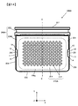
- FIG. 2 is a front view of a case member of the power semiconductor module illustrated in FIG. 1.
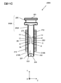
- FIG. 2 is a right side view of a case member of the power semiconductor module illustrated in FIG. 1.
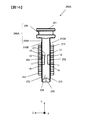
- FIG. 2 is a left side view of a case member of the power semiconductor module illustrated in FIG. 1.
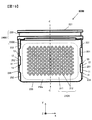
- FIG. 2 is a rear view of a case member of the power semiconductor module illustrated in FIG. 1.
- FIG. 2 is a plan view of a case member of the power semiconductor module illustrated in FIG. 1.
- (A) is a bottom view of the case member of the power semiconductor module shown in FIG. 1, and
- (b) is an enlarged sectional view taken along the line VIIb-VIIb of FIG. FIG.
- FIG. 2 is an exploded perspective view of a case member of the power semiconductor module illustrated in FIG. 1.
- the circuit diagram which shows an example of the circuit of the power semiconductor module of this invention.
- the external appearance perspective view which shows the completion state of the case member produced with the manufacturing method illustrated in FIG. 10, FIG.
- the external appearance perspective view of the power semiconductor module which concerns on Embodiment 2 of this invention.
- FIG. 14 is a front view of a case member of the power semiconductor module illustrated in FIG. 13.
- FIG. 14 is a right side view of a case member of the power semiconductor module illustrated in FIG. 13.
- FIG. 14 is a front view of a case member of the power semiconductor module illustrated in FIG. 13.
- FIG. 14 is a left side view of a case member of the power semiconductor module illustrated in FIG. 13.
- FIG. 14 is a rear view of a case member of the power semiconductor module illustrated in FIG. 13.
- the external appearance perspective view of the power semiconductor module which concerns on Embodiment 3 of this invention.
- the front view of the case member of the power semiconductor module illustrated in FIG. The right view of the case member of the power semiconductor module illustrated in FIG. FIG. 19 is a left side view of a case member of the power semiconductor module illustrated in FIG. 18.
- the rear view of the case member of the power semiconductor module illustrated in FIG. FIG. 19 is an exploded perspective view of a case member of the power semiconductor module illustrated in FIG. 18.
- FIG. 25 is a sectional view taken along line XXV-XXV in FIG. 24.
- FIG. 28 is an external perspective view showing a completed state of a case member manufactured by the manufacturing method shown in FIGS.
- the external appearance perspective view of the power semiconductor module which concerns on Embodiment 4 of this invention.
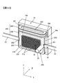
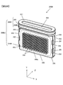
- FIG. 1 is an external perspective view of a power semiconductor module according to an embodiment of the present invention.
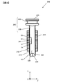
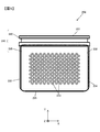
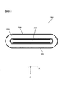
- FIGS. 2 to 7 are a front view and a right side view of a case member of the power semiconductor module shown in FIG. 1, respectively. It is a figure, a left view, a rear view, a plan view, and a bottom view.
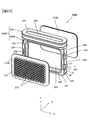
- FIG. 8 is an exploded perspective view of the case member shown in FIG.
- the power semiconductor module 100 is mounted on a vehicle such as a hybrid vehicle or an electric vehicle.
- the power semiconductor module 100 includes a case member 200 and a circuit body 300.
- the circuit body 300 includes a plurality of power semiconductor elements and includes a power conversion circuit that converts DC power into AC power.
- DC power supplied from an alternator driven by a battery (not shown) or an engine is converted into AC power by a power conversion circuit built in the circuit body 300 of the power semiconductor module 100 and supplied to the motor.
- a U-phase, V-phase, and W-phase three-phase bridge circuit can be configured.
- the case member 200 is configured by joining a frame-like case 240 and a metal base 210.
- Both the frame-like case 240 and the metal base 210 are made of an aluminum alloy material, for example, a metal material such as Al, AlSi, AlSiC, Al—C or the like.
- the frame-shaped case 240 has a flange portion 220 and a frame-shaped portion 230 formed below the flange portion 220.
- the flange portion 220 and the frame-like portion 230 are integrally formed by aluminum die casting or the like.
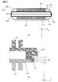
- FIGS. 7 (a), 7 (b) and FIG. 7A is a bottom view of the case member of the power semiconductor module shown in FIG. 1, and FIG. 7B is an enlarged sectional view taken along the line VIIb-VIIb of FIG.
- the frame-shaped portion 230 has a front surface 231, a back surface 232, a pair of side surfaces 233 and 234, and a lower surface 235, and has a substantially rectangular parallelepiped shape.
- a substantially rectangular opening 261 is formed on the front surface 231 of the frame-shaped portion 230 in plan view.
- the opening 261 has an opening edge part slightly inside the outer peripheral side of the front surface 231 of the frame-like part 230, and four corners are edged in an arc shape.
- a step 262 is formed inside the opening edge of the opening 261.
- the step portion 262 is formed by denting the outer surface side of the front surface 231 in the thickness direction and reducing the thickness of this portion (see FIG. 11).
- Radiating fins 213 are formed on the back surface 232 of the frame-shaped portion 230 (see FIGS. 5 and 11).
- the flange portion 220 has a horizontally long upper portion 221 whose both ends have a semicircular arc shape, and connects the front surface 231, the back surface 232, and the pair of side surfaces 233 and 234 of the frame-shaped portion 230.
- a horizontally long through hole 222 is formed at the center of the upper portion 221.
- a storage space for storing the circuit body 300 is formed by the front surface 231, the back surface 232, the pair of side surfaces 233 and 234, and the lower surface 235 of the frame-shaped portion 230, and the through hole 222 of the flange portion 220 communicates with the storage space. To do.
- the circuit body 300 is inserted through the through-hole 222 of the flange portion 220 and is housed in the housing space of the frame-shaped case 240 in a state where each terminal to be described later protrudes above the flange portion 220.
- the side surfaces 233 and 234 of the frame-shaped portion 230 are arc-shaped with the central portion in the thickness direction (Z direction) of the frame-shaped portion 230 bulging outward. It is formed to be curved.
- the arc shape includes partial shapes such as an oval shape, an oval shape, a disc shape, and a dome shape, in addition to a perfect circular shape.
- a first recess 251 and a second recess 252 extending inward of the frame-shaped portion 230 are formed on each of the side surfaces 233 and 234.
- the first and second recesses 251 and 252 are each formed substantially at the center in the height direction (Y direction) of the frame-like portion 230.
- the X direction, Y direction, and Z direction are as shown in the drawings.
- the bottom surfaces 11 of the first and second recesses 251 and 252 in the Z direction are provided on the side closer to the front surface 231 than the intermediate position of the side surfaces 233 and 234 in the thickness direction (Z direction). That is, each bottom surface 11 of the first and second recesses 251 and 252 is formed to a depth that does not reach the middle position in the thickness direction (Z direction). Further, the side end surfaces 12 in the length direction (X direction) of the frame-shaped portion 230 of the first and second recesses 251 and 252 are formed in the regions of the side surfaces 233 and 234 curved in an arc shape, respectively. .
- first and second recesses 251 and 252 are provided in the regions of the side surfaces 233 and 234 that are curved in an arc shape, and open to the front surface 231 and the side surfaces 233 and 234, respectively.
- Each of the first and second recesses 251 and 252 has end faces 13 and 14 that face each other in the height direction (Y direction).
- the metal base 210 includes a substantially flat plate-like portion 211 and a large number of columnar radiating fins 212 formed to protrude from the plate-like portion 211.
- the metal base 210 has an outer peripheral shape that is fitted into the opening 261 of the frame-shaped portion 230. Although details will be described later, the metal base 210 is fitted into the opening 261 of the frame-shaped portion 230 and placed on the stepped portion 262. In this state, the peripheral edge of the plate-like portion 211 and the peripheral edge of the opening 261 of the frame-like portion 230 are joined. As illustrated by a dotted line in FIG. 1, a frame-like joint portion FW in which the metal base 210 is joined by, for example, friction stir welding is formed on the front surface 231 of the case member 200.
- the circuit body 300 incorporates a power semiconductor element that constitutes a power conversion circuit that converts DC power into AC power or AC power into DC power.
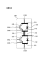
- FIG. 9 is a circuit diagram showing an example of a circuit of the power semiconductor module of the present invention.
- the circuit body 300 includes power semiconductor elements such as an upper arm IGBT 155, an upper arm diode 156, a lower arm IGBT 157, and a lower arm diode 158.
- An upper arm gate terminal 325U and a lower arm gate terminal 325L are connected to the gate electrode of the upper arm IGBT 155 and the gate electrode of the lower arm IGBT 157, respectively.
- An upper arm emitter terminal 326U and a lower arm emitter terminal 326L are connected to the emitter electrode of the upper arm IGBT 155 and the emitter electrode of the lower arm IGBT 157, respectively.
- the collector electrode of the upper arm IGBT 155 and the cathode electrode of the upper arm diode 156 are connected by a DC positive electrode conductor plate 315, and the DC positive electrode conductor plate 315 is connected to a DC positive electrode terminal 315A.
- the emitter electrode of the upper arm IGBT 155 and the anode electrode of the upper arm diode 156 are connected by a second AC conductor plate 318.
- the emitter electrode of the lower arm IGBT 157 and the anode electrode of the lower arm diode 158 are connected by a DC negative conductor plate 319, and the DC negative conductor plate 319 is connected to a DC negative terminal 319A.
- the collector electrode of the lower arm IGBT 157 and the cathode electrode of the lower arm diode 158 are connected by a first AC conductor plate 316.
- the first AC conductor plate 316 and the second AC conductor plate 318 are connected by an intermediate conductor plate 159.
- the first AC conductor plate 316 is connected to the AC output terminal 321.
- circuit housing structure Although the structure of the circuit body 300 is not illustrated, the outline thereof is as follows. As shown in FIG. 9, the upper arm IGBT 155 and the upper arm diode 156 are sandwiched between the DC positive conductor plate 315 and the second AC conductor plate 318 in a state of being thermally coupled to the conductor plates 315 and 318. , Formed as a first semiconductor block. The lower arm IGBT 157 and the lower arm diode 158 are sandwiched between the AC output terminal 321 and the DC negative conductor plate 319 while being thermally coupled to the conductor plates 321 and 319, and are formed as a second semiconductor block.
- the first AC conductor plate 316 and the second AC conductor plate 318 are connected by an intermediate conductor plate 159.
- the first semiconductor block and the second semiconductor block are arranged in the mold such that the DC positive electrode conductor plate 315 and the first AC conductor plate 316 are arranged in the same plane, and each terminal 315A, 325U, 326U, 319A, 321, 325L, and 326L are exposed and sealed.
- the DC positive electrode conductor plate 315 and the first AC conductor plate 316 are flush with the outer surface of the resin on one side and are exposed from the resin.
- the second AC conductor plate 318 and the DC negative electrode conductor plate 319 are flush with the outer surface of the resin on the other surface side and are exposed from the resin.
- the circuit body 300 is exposed to the outside with the conductor plate thermally coupled to the power semiconductor element being flush with the front and back surfaces of the sealing resin.
- the circuit body 300 is inserted from the through hole 222 of the case member 200 and is stored in the storage space of the case member 200.
- the conductor plates formed on both the front and back surfaces of the circuit body 300 are in contact with the inner surface of the metal base 210 and the inner surface of the back surface 232 of the frame-like case 240 so as to allow heat conduction.
- a structure in which a heat conductive sheet is interposed between the circuit body 300 and the metal base 210 and between the circuit body 300 and the inner surface of the back surface 232 of the frame-shaped case 240 may be thermally coupled.
- the frame-shaped case 240 is displaced, and the inner surface of the metal base 210 and the frame The distance in the thickness direction (Z direction) between the inner surface of the back surface 232 of the cylindrical case 240 is not uniform.
- the length from the opening edge of the opening 261 of the frame-shaped portion 230 to the outer peripheral side of the side surfaces 233 and 234 of the frame-shaped portion 230 is increased.
- the frame-shaped case 240 that is, the case member 200 is increased in size.
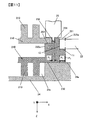
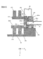
- FIG. 10 is a perspective view for explaining a method of manufacturing the case member of the power semiconductor module shown in FIG. 1, and FIG. 11 is a cross-sectional view taken along line XI-XI in FIG.
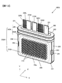
- FIG. 12 is an external perspective view showing a completed state of the case member 200 manufactured by the manufacturing method shown in FIGS.
- the metal base 210 is joined to the frame-shaped case 240 without displacing the frame-shaped case 240, and the case member 200 is attached. It is important to make.
- the frame-like case 240 is held by the jig 24.
- the receiving jig 24 is formed in a substantially rectangular shape, and has a support surface 24a and a groove portion 24b.
- a recess 24c (see FIG. 11) is formed in a region corresponding to the heat radiation fin 213 provided on the back surface 232 of the frame-like case 240.
- the heat dissipating fins 213 are arranged in the recesses 24c so that the back surface 232 of the frame-like case 240 is placed on the support surface 24a, and also protrudes from the back surface 232 of the flange portion 220 into the groove portion 24b of the receiving jig 24. Accommodates part.
- the opening 261 of the frame-like case 240 is arranged on the upper side opposite to the receiving jig 24.
- the plate-like part 211 of the metal base 210 is fitted into the opening part 261 of the frame-like case 240 and placed on the step part 262 formed on the peripheral edge part of the opening part 261.
- the mounting surface of the metal base 210 of the stepped portion 262 may be a cast surface, or may be subjected to cutting as necessary.
- the depth of the stepped portion 262 and the plate so that the upper surface of the metal base 210 and the upper surface of the front surface 231 of the frame-shaped portion 230 are substantially flush with each other. It is preferable to set the thickness of the shape portion 211.
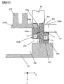
- the bottom surface 11 of each of the first recess 251 formed on the side surface 233 of the frame-shaped case 240 and the second recess 252 formed on the side surface 234 is pressed by the fixing jig 23 to fix the frame-shaped case 240.
- the frame-like case 240 needs to be fixed in the X, Y, and Z directions.
- the fixing jig 23 fixes the first and second recesses 251 and 252 in the Z direction by pressing the bottom surface 11 against the jig 24. That is, the frame-like case 240 is fixed in the X direction by bringing the front end surface of each fixing jig 23 into contact with the side end surfaces 12 of the first and second recesses 251 and 252.
- the frame-shaped case 240 is fixed in the Y direction by pressing the side surfaces of the fixing jigs 23 against the end surfaces 13 and 14 of the first and second recesses 251 and 252.
- one fixing jig 23 is provided on one end face of the end faces 13 and 14 of the first recess 251
- the other fixing jig 23 is provided on the other end face of the end faces 13 and 14 of the second recess 252. It is good to push.
- the frame-shaped case 240 can be fixed in the X direction and the Y direction by pressing the outer peripheral side surface of the frame-shaped case 240. That is, in order to fix the frame-shaped case 240 in the X direction, the side surfaces 233 and 234 of the frame-shaped case 240 may be held by a fixing jig different from the fixing jig 23. Further, in order to fix the frame-shaped case 240 in the Y direction, the lower surface 235 of the frame-shaped case 240 and the upper surface of the upper portion 221 of the flange portion 220 may be held by a fixing jig different from the fixing jig 23.
- the first and second recesses 251 and 252 are open to the front surface 231 side of the frame-shaped part 230. It is only necessary to move in the direction and press the bottom surface 11 of the first and second recesses 251 and 252. Therefore, the frame-shaped case 240 can be fixed efficiently.
- FIG. 11 is a diagram for explaining a method of joining the frame-shaped case 240 and the metal base 210 on the side surface 233 side of the frame-shaped case 240, but the following description will be given on the side surface 234 side of the frame-shaped case 240. Is the same.
- the fixing jig 23 mounted on the bottom surface 11 of the first concave portion 251 of the frame-shaped case 240 has a depth of the bottom surface 11 of the first concave portion 251 such that the upper surface is lower than the front surface 231 of the frame-shaped portion 230.
- the thickness of the fixing jig 23 is set.
- the outer peripheral edge of the metal base 210 and the peripheral edge of the opening 261 of the frame-shaped case 240 are bonded by, for example, friction stir welding using the bonding tool 25.
- the end surface of the welding tool 25 is disposed so as to correspond to the outer peripheral side surface of the metal base 210 and the abutting surface of the opening portion 261 of the frame-like case 240, and extends over the entire circumference of the opening portion 261 along the abutting surface.
- the joining tool 25 is moved. Thereby, the metal base 210 and the frame-shaped case 240 are joined by the joint part FW.
- the first recess 251 when projected from the thickness direction (Z direction) of the frame-like case 240, the first recess 251 has a projection part P 1 on the outside of the projection part P 2 of the joint part FW. Has been placed. That is, the side end surface 12 in the length direction (X direction) of the first recess 251 is located outside the joint portion FW. For this reason, the load at the time of joining by the joining tool 25 can be supported by the part between the inner surface 230a and the side end face 12 in the frame-like part 230 of the frame-like case 240, and the frame-like case 240 by the load at the time of joining. Can be prevented from being deformed.
- the first recessed portion 251 is arranged such that the projected portion P 1 overlaps the side 233 a of the side surface 233.
- the bottom surface 11 of the first recess 251 is provided in the region of the side surface 233 curved in an arc shape, and the bottom surface 11 of the first recess 251 is directly opened outward from the side surface 233. Yes.
- the first recess 251 is provided in the region of the side surface 233 curved in an arc shape, and the bottom surface 11 of the first recess 251 is directly opened outward from the side surface 233. Yes.
- the frame-like case 240 can be made smaller than the structure in which the frame is provided.
- FIG. 12 is an external perspective view showing a completed state of the case member 200 manufactured by the above-described method.
- the circuit body 300 is inserted into the case member 240 from the through hole 222 of the flange portion 220, and each terminal protrudes above the flange portion 220.
- the power semiconductor module 100 shown in FIG. 1 is formed.
- a resin may be injected into the gap between the circuit body 300 and the case member 200 and cured.
- First and second recesses 251 and 252 are provided on the side surfaces 233 and 234 of the frame-like case 240, and the bottom surface 11 of the first and second recesses 251 and 252 is pressed in the Z direction by the fixing jig 23. It fixed on the upper surface 24a of the jig
- the circuit member 300 can be favorably cooled by the case member 200 without increasing the size of the case member 200.
- the first recess 251 When projected from the thickness direction (Z direction) of the frame-like case 240, the first recess 251 has a structure in which the projected portion P 1 is disposed outside the projected portion P 2 of the joint portion FW. (See FIG. 11). That is, the side end surface 12 in the length direction (X direction) of the first recess 251 is located outside the joint FW, and the side end surface 12 in the X direction of the first recess 251 is located inside the joint FW. Not located. For this reason, the load by the joining tool 25 can be supported by the portion of the frame-shaped portion 230 between the inner surface 230a of the frame-shaped portion 230 and the side end surfaces 12 of the first and second recesses 251 and 252. The deformation of the case 240 can be prevented.
- the first recessed portion 251 When projected from the thickness direction (Z direction) of the frame-shaped case 240, the first recessed portion 251 is arranged such that the projected portion P 1 thereof overlaps the side 233a of the side surface 233 (see FIG. 11). ). Since the bottom surface 11 of the first recess 251 is provided in the region of the side surface 233 curved in an arc shape, the frame-shaped case 240 can be made small. Further, since the bottom surface 11 of the first recess 251 is directly open outward from the side surface 233, the frame-shaped case 240 can be made small also by this structure.
- the first and second recesses 251 and 252 are open toward the front surface 231 of the frame-like case 240. Therefore, the frame-shaped case 240 can be fixed by moving the fixing jig 23 in the Z direction and pressing the bottom surfaces 11 of the first and second recesses 251 and 252. Can be done efficiently.
- FIG. 13 is an external perspective view of a power semiconductor module according to Embodiment 2 of the present invention.
- 14 to 17 are a front view, a right side view, a left side view, and a rear view of the case member of the power semiconductor module shown in FIG. 13, respectively.
- the power semiconductor module 100A of the second embodiment is different from the power semiconductor module 100 of the first embodiment in that the case member 200A has a structure that is bonded to the metal bases 210A and 210B on both the front and back surfaces.
- the front surface 231 of the frame-shaped case 240A is joined to the metal base 210A
- the rear surface 232 of the frame-shaped case 240A is joined to the metal base 210B.
- the second embodiment will be described mainly with respect to differences from the first embodiment, and the same components as those in the first embodiment will be denoted by the same reference numerals, and the description thereof will be omitted as appropriate.
- the frame-shaped case 240A has openings 261 shown in FIG. 8 on both the front surface 231 and the back surface 232, and the metal bases 210A and 210B are respectively the front surface 231 and the back surface 232 of the frame-shaped case 240A.
- the openings 261 are fitted, and the peripheral portions of the metal bases 210A and 210B and the peripheral portion of the opening 261 of the frame-like case 240A are joined by the joint portions FWa and FWb.
- the metal bases 210 ⁇ / b> A and 210 ⁇ / b> B are the same members as the metal base 210 of the first embodiment, and each have a heat radiation fin 212.
- a first recess 251 and a second recess 252 are formed on the side surfaces 233 and 234 on the front surface 231 side of the frame-shaped case 240A, respectively.
- the first recess 251 and the second recess 252 are formed symmetrically with respect to the central axis CC (see FIG. 14) in the length direction (X direction) of the frame-like case 240A.
- a third recess 253 and a fourth recess 254 are formed on the side surfaces 233 and 234 on the back surface 232 side of the frame-shaped case 240A, respectively.
- the third recess 253 and the fourth recess 254 are formed symmetrically with respect to the central axis CC (see FIG. 17) in the length direction (X direction) of the frame-like case 240.
- the first to fourth recesses 251 to 254 all have the same length in the height direction (Y direction) and the length direction (X direction), and are formed in the same shape.
- the bottom surfaces 11 of the first and second recesses 251 and 252 are arranged on the front surface 231 side from the central portion in the thickness direction (Z direction) of the frame-like case 240A. Further, the bottom surfaces 11 of the third and fourth recesses 253 and 254 are disposed on the back surface 232 side from the central portion in the thickness direction (Z direction) of the frame-like case 240A. Accordingly, as shown in FIG. 15, the bottom surface 11 of the first recess 251 and the bottom surface 11 of the third recess 253 are opposed to the same position in the height direction (Y direction) on the side surface 233 of the frame-like case 240A.
- the bottom surface 11 of the first recess 251 and the bottom surface 11 of the third recess 253 are spaced apart.
- the first concave portion 251 and the third concave portion 253 are arranged with the partition wall portion 271 therebetween.
- the bottom surface 11 of the second recess 252 and the bottom surface 11 of the fourth recess 254 are separated from each other, in other words, the second recess 252 and the fourth recess 254 are partition walls.
- the portion 271 is disposed.
- the metal base 210A is inserted into the opening 261 of the front surface 231 of the frame-like case 240A by the method described in the first embodiment, and the joining tool 25 is used. And joined by friction stir welding or the like. As a result, a joint portion FWa is formed at the peripheral edge of the opening 261 of the front surface 231 of the frame-like case 240A and the peripheral edge of the metal base 210A.
- the fixing jig 23 is raised in the thickness direction (Z direction), the frame-like case 240A is rotated 180 degrees with the central axis CC as the rotation axis, and the frame-like case 240A to which the metal base 210A is bonded is obtained. It is supported by the receiving jig 24. Then, the fixing jig 23 is lowered, and the bottom surface 11 of the third and fourth recesses 253 and 254 formed on the side surfaces 233 and 234 of the frame-like case 240A is received and pressed to the jig 24 side and fixed.
- the first and second recesses 251 and 252 are formed symmetrically with respect to the center axis CC on the front surface 231 side, and the third and fourth recesses 253 and 254 are formed on the center axis C on the back surface 232 side. It is formed symmetrically with respect to -C.
- the third and fourth recesses 253 and 254 are arranged at the same positions as the first and second recesses 251 and 252 before being inverted. Therefore, the bottom surface 11 of the third and fourth recesses can be pressed only by lowering the fixing jig 23 in the thickness direction (Z direction), and alignment with the third and fourth recesses 253 and 254 is achieved. There is no need to do. Thereby, fixation of frame-like case 240A can be performed efficiently.
- the metal base 210B is inserted into the opening 261 of the back surface 232 of the frame-like case 240A. Then, the metal base 210B and the frame-shaped case 240A are joined by friction stir welding or the like using the joining tool 25. Thereby, the joining part FWb is formed in the peripheral part of the opening part 261 of the back surface 232 of the frame-like case 240A and the peripheral part of the metal base 210B.
- the positional relationship in the X direction between the side end surface 12 of the third and fourth concave portions 253 and 254 and the joint portion FWb is the same as the positional relationship in the X direction of the side end surface 12 of the first and second concave portions 251 and 252 and the joint portion FWa. It is. That is, when projected from the thickness direction (Z direction) of the frame-like case 240A, the first and second recesses 251 and 252 have the projected portion P 1 arranged outside the projected portion of the joint portion FWa. 1, the second recess 251 and 252, the projection portion P 1 is the side of the side surface 233 side 233a, are disposed to overlap with the bevel portion P 3 of 234a (not shown).
- the third and fourth recesses 253 and 254 when projected from the thickness direction (Z direction) of the frame-shaped case 240A, the third and fourth recesses 253 and 254 have their projected portions arranged outside the projected portion of the joint FWb, and the third The fourth recesses 253 and 254 are arranged so that the projected portions thereof overlap with the shaded portions of the side edges 233a and 234a (not shown) of the side surfaces 233 and 234, respectively.
- the first and second concave portions 251 and 252 or the third and fourth concave portions 253 and 254 are provided on the side surfaces 233 and 234 on the front surface 231 side and the rear surface 232 side of the frame-shaped case 240A, respectively, and a fixing jig is provided.
- the bottom surface 11 of the first recess 251 to the fourth recess 254 is pressed and fixed in the thickness direction (Z direction).
- the frame-shaped case 240A and the metal base 210A, or the frame-shaped case 240A and the metal base 210B are bonded to each other. Therefore, the same effects as (1) to (4) of the first embodiment are obtained.
- Embodiment 2 has the following effects. (5) Since the metal bases 210A and 210B are joined to the front and back surfaces of the frame-shaped case 240A, in other words, the opening 261 of the frame-shaped case 240A penetrates the front and back surfaces and is wide on the back surface 232 Since it is not necessary to form a thin plate region having an area, molding by casting is facilitated, and productivity and yield can be improved. (6) Further, the first and second recesses 251 and 252 and the third and fourth recesses 253 and 254 are centered in the length direction (X direction) on the front surface 231 side and the back surface 232 of the frame-like case 240A, respectively. They are arranged symmetrically with respect to the axis CC.
- the frame-shaped case 240A when the frame-like case 240A is reversed with the central axis CC as the rotation axis, the third and fourth recesses 253 and 254 are arranged at the same positions as the positions of the first and second recesses 251 and 252 before the inversion. Is done. Accordingly, the frame-shaped case 240A can be fixed by the fixing jig 23 without performing alignment with the third and fourth recesses 253, 254, and the frame-shaped case 240A can be efficiently fixed. Can do.
- FIG. 18 is an external perspective view of a power semiconductor module according to Embodiment 3 of the present invention.
- 19 to 22 are a front view, a right side view, a left side view, and a rear view of the case member of the power semiconductor module shown in FIG. 18, respectively.
- FIG. 23 is an exploded perspective view of the case member shown in FIG. Embodiment 3 differs from Embodiment 2 in that a plurality of first to fourth recesses are formed.
- aspects of the third embodiment will be described mainly with respect to differences from the second embodiment, and the same components as those of the second embodiment are denoted by the same reference numerals, and description thereof will be omitted as appropriate. I decided to.
- the power semiconductor module 100B of the third embodiment has a structure in which the case member 200B is joined to the metal bases 210A and 210B on both the front and back surfaces.
- the frame-like case 240B has joints FWa and FWb with the metal bases 210A and 210B on the front surface 231 and the back surface 232, respectively.
- a plurality of first recesses 251 are formed on the side surface 233 of the frame-shaped case 240B on the front surface 231 side, and a plurality of second recesses 252 are formed on the side surface 234 on the front surface 231 side.
- the number of the first recesses 251 and the number of the second recesses 252 formed on the side surface 233 is different, and the even number (two in the embodiment) of the first recesses 251 is formed on the side surface 233. Are formed with odd (three in the embodiment) second recesses 252.
- a plurality of third recesses 253 are formed on the side surface 233 of the frame-like case 240B on the back surface 232 side, and a plurality of fourth recesses 254 are formed on the side surface 234.
- the number of first recesses 251 formed on the side surface 233 on the front surface 231 side is equal to the number of fourth recesses 254 formed on the side surface 234 on the back surface 232 side.
- the number of second recesses 252 formed on the side surface 234 on the front surface 231 side is equal to the number of third recesses 253 formed on the side surface 234 on the back surface 232 side.
- first concave portion 251 and the fourth concave portion 254 are formed symmetrically with respect to the central axis CC in the length direction (X direction) of the frame-like case 240.
- the second recess 252 and the third recess 253 are formed symmetrically with respect to the central axis CC in the length direction (X direction) of the frame-like case 240.
- the first to fourth recesses 251 to 254 all have the same length in the height direction (Y direction) and the length direction (X direction), and are formed in the same shape.
- each fourth recess 254 overlap the position and shape of each first recess 251 before rotation, and each third The position and shape of the recess 253 overlap the position and shape of each second recess 252 before rotation.
- each first recess 251 and each third recess 253 are formed at positions shifted in the height direction (Y direction) on the side surface 233.
- the center of each first recess 251 in the height direction (Y direction) is located substantially at the center between the third recesses 253, and the upper and lower ends of each first recess 251 are one end of the upper and lower third recesses 253. And it arrange
- each second recess 252 and each fourth recess 254 are formed at positions shifted in the height direction (Y direction) on the side surface 234.
- each second recess 252 in the height direction is located substantially at the center between the fourth recesses 254, and the upper and lower ends of each second recess 252 are one end of the upper and lower fourth recesses 254. And it arrange
- the bottom surfaces 11 of the first and second recesses 251 and 252 are disposed closer to the front surface 231 than the center in the thickness direction (Z direction) of the frame-like case 240B, and the bottom surfaces 11 of the third and fourth recesses 253 and 254 are
- the frame-shaped case 240B is disposed on the back surface 232 side from the center portion in the thickness direction (Z direction). Accordingly, as illustrated in FIGS. 20 and 21, the bottom surfaces 11 of the first recesses 251 and the third recesses 253 and the bottom surfaces 11 of the second recesses 252 and the fourth recesses 254 are provided on both sides of the partition wall portion 272. Opposed to each other.
- first and second recesses 251 and 252 or one of the third and fourth recesses 253 and 254 are not formed in the central region of the partition wall portion 272
- the first and second recesses 251 and 252 or the second 3 and the fourth recesses 253 and 254 have rigidity higher than that of the partition wall portion 271 of the second embodiment formed in the opposing region.
- FIG. 24 is a perspective view for explaining a method of manufacturing the case member shown in FIG. 18, and FIG. 25 is a sectional view taken along line XXV-XXV in FIG.
- FIG. 26 is a perspective view for explaining a step following FIG. 24, and FIG. 27 is a cross-sectional view taken along line XXVII-XXVII in FIG.
- FIG. 28 is an external perspective view of the case member of the power semiconductor module according to Embodiment 3 of the present invention.
- the frame-like case 240B is held by the jig 24.
- the metal base 210A is fitted into the opening 261 of the front surface 231 of the frame-shaped case 240B, and is placed on the stepped portion 262 (see FIG. 8) formed at the peripheral edge of the opening 261 of the frame-shaped case 240B. .
- the bottom surface 11 of each first recess 251 and the bottom surface 11 of each second recess 252 are pressed by the fixing jig 23 to fix the frame-shaped case 240B.
- the fixing jig 23 uses two that press the bottom surface 11 of the first recess 251 formed on the front surface 231 side and three that press the bottom surface 11 of the second recess 252.
- the metal base 210A and the front surface 231 of the frame-like case 240B are joined by friction stir welding or the like.
- the joining part FWb is formed in the peripheral part of the opening part 261 of the front surface 231 of the frame-like case 240B and the peripheral part of the metal base 210A.
- FIG. 25 is a sectional view taken along the line XXV-XXV in FIG. 24 in the bonded state.
- This state is the same as that of the first embodiment except that the opening 263 is formed on the back surface 232 of the frame-like case 240B. That is, when projected in the thickness direction of the frame-shaped casing 240B (Z-direction), each first recess 251, the projection portion P 1 is disposed outside the projection portion P 2 of the joint FWA.
- the projected portion P 1 of each first recess 251 is the side 2 of the side surface 233. 33a is arranged so as to overlap.
- the position and shape of the third recess 253 overlap the position and shape of the second recess 252 before rotation. That is, in FIG. 26, the two fourth recesses 254 and the three third recesses 253 provided on the back surface 232 side are the two first recesses 251 and the three second recesses before the frame-like case 240B is reversed. The position and shape of the recess 252 overlap each other. For this reason, the bottom surfaces 11 of the fourth concave portion 254 and the third concave portion 253 are received on the jig 24 side by simply lowering the five fixing jigs 23 that have been raised in the thickness direction (Z direction). It can be pressed and fixed.
- the metal base 210B is inserted into the opening 263 on the back surface 232 of the frame-like case 240B and placed on the step 264 (see FIG. 27) formed on the peripheral edge of the opening 263 of the frame-like case 240B. Then, the metal base 210B and the frame-like case 240B are joined by friction stir welding or the like using the joining tool 25. Thereby, the joining part FWb is formed in the peripheral part of the opening part 263 of the back surface 232 of the frame-shaped case 240B and the peripheral part of the metal base 210B.
- the bottom surface 11 of the third and fourth recesses 253 and 254 can be pressed only by lowering the fixing jig 23 in the Z direction. 3, it is not necessary to align with the 4th recessed part 253,254. For this reason, the frame-like case 240B can be efficiently fixed.
- FIG. 27 is a sectional view taken along the line XXVII-XXVII in FIG. 26 in the joined state.
- the positional relationship between the fourth recess 254 and the joint FWb is the same as the positional relationship between the first recess 251 and the joint FWa. That is, when projected from the thickness direction (Z direction) of the frame-shaped case 240B, the projections P 4 of the fourth recesses 254 are arranged outside the projection P 5 of the joint FWb.
- the projected portion P 4 of each fourth recess 254 is disposed so as to overlap with the projected portion P 6 of the side 234 a of the side surface 234.
- the length of the shaded portion P 4 of the fourth recesses 253 and 254 may be the same as or different from the length of the shaded portion P 1 of the first recess 251.
- the projection part P 4 of each fourth recess 254 may be arranged outside the projection part P 5 of the joint part FWb.
- the third embodiment is different from the second embodiment only in that the number of the first recesses 251 to the fourth recesses 254 is plural. Therefore, also in the third embodiment, the effects 1 to 5 of the second embodiment are achieved.
- the partition wall 272 includes a thick region where the first recess 251 and the third recess 253 do not face each other or a thick region where the second recess 252 and the fourth recess 254 do not face each other. It has a rigidity higher than that of the partition wall portion 271 of the second mode. Therefore, the deformation of the frame-like case 240B at the time of joining can be made smaller than in the case of the second embodiment, so that the dimensional accuracy of the storage space formed in the case member 200B can be further improved.
- the first and third recesses 251 and 253 and the second and fourth recesses 252 and 254 are illustrated as different structures.
- the numbers of the first recesses 251 and the third recesses 253 or the numbers of the second recesses 252 and the fourth recesses 254 may be the same.
- increasing the rigidity of the partition wall by shifting the positions of the first and third recesses 251 and 253 formed on the side surface 233 and the positions of the second and fourth recesses 252 and 254 formed on the side surface 234 side,
- the length is symmetrical with respect to the central axis CC in the length direction (X direction).
- the first and fourth recesses 251 and 254 are made to be frame-like portions 230B in the height direction (Y direction).
- the second and third recesses 252 and 253 can be arranged outside the first and fourth recesses 251 and 254 in the height direction (Y direction). Even if it arrange
- the number of the first recesses 251 to the fourth recesses 254 is not limited to two.
- Embodiment 4 29 is an external perspective view of a power semiconductor module according to Embodiment 4 of the present invention
- FIG. 30 is a cross-sectional view taken along line XXX-XXX in FIG.
- the first and second recesses 251a and 252a formed in the case member 200C are opened only to the side surface 233 or the side surface 234 of the frame-like case 240C, and the front surface 231 and the back surface 232 are Not open.
- the height (length in the Z direction) of the first and second recesses 251 a and 252 a is formed larger than the thickness of the fixing jig 23.
- the fixing jig 23 is moved in the length direction (X direction) from the outside of the side surfaces 233 and 234 toward the frame-shaped case 240C side. And fit into the first recess 251a or the second recess 252a. Then, the fixing jig 23 is lowered in the thickness direction (Z direction) and fixed. The front end surface of the fixing jig 23 may be brought into contact with the side end surfaces 12 of the first and second recesses 251a and 252a to fix the frame-shaped case 240C in the length direction (X direction).
- the side surface of the fixing jig 23 may be in contact with the end surfaces 13 and 14 of the first and second recesses 251a and 252a to fix the frame-shaped case 240C in the height direction (Y direction).
- One or both of the length direction (X direction) and the height direction (Y direction) of the frame-shaped case 240C is pressed and fixed from the side surface, the upper surface, and the lower surface of the frame-shaped case 240C using another fixing jig. You can also
- the first recess 251a when projected from the thickness direction (Z direction) of the frame-like case 240C, the first recess 251a has a projection part P 1a inside the projection part P 2 of the joint part FW. Has been extended to. That is, the side end surface 12 in the X direction of the first recess 251a is located on the inner side of the joint portion FW. This structure is the same also about the 2nd recessed part 252a. Since the first recesses 251a and 252a are not open to the front surface 231 of the frame-like case 240C and are formed below the front surface 231, they do not hinder the bonding by the bonding tool 25.
- the first recessed portion 251a When projected from the thickness direction (Z direction) of the frame-like case 240, the first recessed portion 251a is arranged such that the projected portion P 1a thereof is overlapped with the side 233a of the side surface 233. It is the same. Since other configurations in the fourth embodiment are the same as those in the first embodiment, the corresponding members are denoted by the same reference numerals and description thereof is omitted.
- the first and second recesses 251a and 252a are provided on the side surfaces 233 and 234 of the frame-like case 240C, and the bottom surface 11 of the first and second recesses 251a and 252a is formed in the thickness direction by the fixing jig 23.
- the metal base 210 and the frame-like case 240C can be joined in this fixed state. Therefore, the effect 1 of Embodiment 1 is produced.
- the side end surface 12 in the length direction (X direction) of the first and second recesses 251a and 252a is located on the inner side of the joint FW.
- the length between the opening of the front surface 231 and the side surfaces 233 and 234 in the frame-like case 240C can be made smaller than those in the first to third embodiments, and the case member 200 can be further reduced in size. be able to.
- Embodiment 4 has been exemplified as a power semiconductor module including the case member 200C in which the first and second recesses 251a and 252a are formed on the side surfaces 233 and 234 on the front surface 231 side of the frame-like case 240C.
- the first concave portion 251 to the fourth concave portion 254 in the second embodiment or the third embodiment may have the same structure as the first and second concave portions 251a and 252a in the fourth embodiment.
- the side surfaces 233 and 234 are exemplified as a structure having a curved shape, but the side surfaces 233 and 234 may have a flat shape.
- the case members 200, 200A to 200C are exemplified as structures having the radiation fins 212, 213.
- the case members 200, 200A to 200C do not have the radiation fins 212, 213. Also good.
- the circuit body 300 is exemplified as a structure including two semiconductor blocks formed by sandwiching a semiconductor element between a pair of conductor plates.
- the present invention can also be applied to the case where the circuit body 300 includes one or more semiconductor blocks.
- the conductor plate may be arranged on only one surface side of the semiconductor element, and the structure of the semiconductor block is not limited to the above embodiment.
- the present invention can be applied to a power semiconductor module in which the circuit body 300 includes a power conversion circuit such as an inverter circuit or a converter circuit.
- a power conversion circuit such as an inverter circuit or a converter circuit.
- first to fourth recesses 251 to 254 are exemplified as structures formed only on the side surfaces 233 and 234.
- recesses other than the first recesses 251 to the fourth recesses 254 may be formed on the lower surfaces 235 of the case members 200 and 200A to 200C.
- the power semiconductor module of the present invention can be variously modified and applied within the scope of the invention.
- the power semiconductor module can be applied to each of the pair of opposite side surfaces of the frame-shaped case from the side surfaces. What is necessary is just to equip the inside of a case member and the case member provided with the case member in which the recessed part which has the bottom face formed facing the junction part side was formed in the intermediate position of the thickness of the side surface.
Landscapes
- Engineering & Computer Science (AREA)
- Power Engineering (AREA)
- Cooling Or The Like Of Semiconductors Or Solid State Devices (AREA)
- Inverter Devices (AREA)
Abstract
Description
このため、パワー半導体モジュールのケースは、通常、金属により形成される。ケースは、パワー半導体素子等の電子部品を有する回路体が収納される収納空間を備えている。
特許文献1に記載された構造では、金属枠体の開口部周縁部の幅が小さく、金属枠体を確実に固定することができない。金属枠体の開口部周縁部の幅を十分な大きさとすると、パワー半導体モジュールが大型化する。
本発明のパワー半導体モジュールの製造方法は、上記パワー半導体モジュールの製造方法であって、枠状ケースの開口部に金属ベースを嵌入する、枠状ケースの一対の側面のそれぞれに形成された凹部の底面を固定治具により少なくとも側面の厚さ方向に固定する、枠状ケースの開口部の周縁部と金属ベースの周縁部とを接合し、ケース部材を形成する、ケース部材に回路体を収納する、の各工程を備える。
[パワー半導体モジュールの構造]
以下、図面を参照して本発明によるパワー半導体モジュールおよびパワー半導体モジュールの一実施の形態を詳細に説明する。
図1は、本発明の一実施の形態に係るパワー半導体モジュールの外観斜視図であり、図2~図7は、それぞれ、図1に図示されたパワー半導体モジュールのケース部材の正面図、右側面図、左側面図、背面図、平面図および下面図である。また、図8は、図1に図示されたケース部材の分解斜視図である。
パワー半導体モジュール100は、ハイブリッド自動車や電気自動車等の車両に搭載される。パワー半導体モジュール100は、ケース部材200と回路体300とを備える。
回路体300は、複数のパワー半導体素子を有し、直流電力を交流電力に変換する電力変換回路を備えている。不図示のバッテリやエンジンにより駆動されるオルタネータから供給される直流電力は、パワー半導体モジュール100の回路体300に内蔵された電力変換回路により交流電力に変換されてモータに供給される。パワー半導体モジュール100を3個用い、各パワー半導体モジュール100の回路体300を接続して、U相、V相、W相の3相ブリッジ回路を構成することができる。
枠状ケース240は、フランジ部220と、フランジ部220の下方に形成された枠状部230とを有する。フランジ部220と枠状部230は、アルミダイキャスト等により一体成形される。
図7(a)は、図1に図示されたパワー半導体モジュールのケース部材の下面図であり、図7(b)は、図1のVIIb-VIIb線拡大断面図である。
枠状部230は、前面231と、裏面232と、一対の側面233、234と、下面235とを有し、ほぼ直方体形状を有する。枠状部230の前面231には、平面視でほぼ矩形形状の開口部261が形成されている。開口部261は、枠状部230の前面231の外周側辺の僅かに内側に開口縁部を有し、4つの角部は、円弧状に縁取りされている。開口部261の開口縁部の内側には、段部262が形成されている。段部262は、前面231の外面側を厚さ方向に凹ませ、この部分の板厚を薄くして(図11参照)形成されたものである。枠状部230の裏面232には、放熱フィン213が形成されている(図5、図11参照)。
枠状部230の前面231と、裏面232と、一対の側面233、234と、下面235とにより回路体300を収納する収納空間が形成され、フランジ部220の貫通孔222は、収納空間に連通する。回路体300は、フランジ部220の貫通孔222から挿入され、後述する各端子をフランジ部220の上方に突き出した状態で、枠状ケース240の収納空間に収納される。
ぞれ、枠状部230の厚さ方向(Z方向)の中央部が外側に膨らむ円弧状に湾曲して形成されている。ここで、円弧状とは、真円の部分形状以外、長円形、楕円形、円板状、ドーム状などの部分形状を含む。
図7(b)、図8に示すように、側面233、234のそれぞれには、枠状部230の内方に延在する第1凹部251、第2凹部252が形成されている。第1、第2凹部251、252は、それぞれ、枠状部230の高さ方向(Y方向)のほぼ中央に形成されている。なお、X方向、Y方向、Z方向は、各図に図示の通りとする。
第1、第2凹部251、252それぞれは、高さ方向(Y方向)において相対向する端面13、14を有する。
図1に点線で図示されるように、ケース部材200の前面231には、金属ベース210が、例えば、摩擦攪拌接合により接合された枠状の接合部FWが形成されている。
回路体300は、直流電力を交流電力に、または交流電力を直流電力に変換する電力変換回路を構成するパワー半導体素子を内蔵している。
図9は、本発明のパワー半導体モジュールの回路の一例を示す回路図である。
回路体300は、上アームIGBT155、上アームダイオード156、下アームIGBT157、下アームダイオード158等のパワー半導体素子を有する。
上アームIGBT155のゲート電極と下アームIGBT157のゲート電極には、それぞれ、上アームゲート端子325U、下アームゲート端子325Lが接続される。上アームIGBT155のエミッタ電極と下アームIGBT157のエミッタ電極には、それぞれ、上アームエミッタ端子326U、下アームエミッタ端子326Lが接続される。
下アームIGBT157のエミッタ電極と下アームダイオード158のアノード電極は直流負極導体板319により接続され、直流負極導体板319は直流負極端子319Aに接続される。下アームIGBT157のコレクタ電極と下アームダイオード158のカソード電極は第一交流導体板316により接続される。
第一交流導体板316と第二交流導体板318とは中間導体板159により接続される。
第一交流導体板316は、交流出力端子321に接続される。
図1に図示された回路体300の各端子に付された参照番号は、図9に図示された上記各端子の参照番号と一致する。
回路体300の構造は図示されないが、その概要は以下の通りである。
図9に図示されるように、上アームIGBT155と上アームダイオード156は、直流正極導体板315と第二交流導体板318との間に、各導体板315、318に熱結合した状態で挟持され、第1半導体ブロックとして形成される。下アームIGBT157と下アームダイオード158は、交流出力端子321と直流負極導体板319との間に、各導体板321、319に熱結合した状態で挟持され第2半導体ブロックとして形成される。第一交流導体板316と第二交流導体板318とは中間導体板159により接続される。第1半導体ブロックと第2半導体ブロックとは、直流正極導体板315と第一交流導体板316とが同一平面となるように並べて金型内に配置され、モールド成形により、各端子315A、325U、326U、319A、321、325L、326Lを露出して封止される。このとき、直流正極導体板315と第一交流導体板316とは、一面側において樹脂の外表面と同一面とされ、樹脂から表出される。また、第二交流導体板318と直流負極導体板319とは、他面側において樹脂の外表面と同一面とされ、樹脂から表出される。
回路体300は、ケース部材200の貫通孔222から挿入され、ケース部材200の収納空間内に収納される。収納空間内に収納された状態で、回路体300の表裏両面に形成された導体板が、金属ベース210の内面および枠状ケース240の裏面232の内面に熱伝導可能に接触する。図示はしないが、回路体300と金属ベース210との間、および回路体300と枠状ケース240の裏面232の内面との間に熱伝導シートを介在して熱結合する構造としてもよい。
接合時における枠状ケース240の固定を確実にするために、枠状部230の開口部261の開口縁部から枠状部230の側面233、234の外周側辺までの長さを大きくすることが考えられるが、これでは、枠状ケース240、すなわち、ケース部材200が大型化することになる。
以下、ケース部材200を大型化することなく、枠状ケース240を確実に固定して、枠状ケース240と金属ベース210とを精度よく接合する、本発明によるパワー半導体モジュールの製造方法の一実施の形態を説明する。
図10は、図1に図示されたパワー半導体モジュールのケース部材の製造方法を説明するための斜視図であり、図11は、図10のXI-XI線断面図である。また、図12は、図10、図11に図示された製造方法で作製されたケース部材200の完成状態を示す外観斜視図である。
上述した通り、回路体300の冷却が均一且つ能力が大きいパワー半導体モジュール100を作製するには、枠状ケース240を変位させることなく金属ベース210を枠状ケース240に接合し、ケース部材200を作製することが重要である。
ケース部材200を作製するには、先ず、枠状ケース240を受け治具24にて保持する。受け治具24は、ほぼ矩形状に形成され、支持面24aと溝部24bとを有する。支持面24aには、枠状ケース240の裏面232に設けられた放熱フィン213に対応する領域に凹部24c(図11参照)が形成されている。この凹部24c内に放熱フィン213を配置して、枠状ケース240の背面232を支持面24a上に載置し、また、受け治具24の溝部24b内にフランジ部220の裏面232から突出する部分を収容する。
固定治具23により、枠状ケース240をZ方向に固定する場合、第1、第2凹部251、252は、枠状部230の前面231側に開放されているので、固定治具23をZ方向に移動して第1、第2凹部251、252の底面11を押圧すればよい。従って、枠状ケース240の固定を能率的に行うことができる。
枠状ケース240の第1凹部251の底面11上に搭載された固定治具23は、その上面が、枠状部230の前面231よりも低くなるように、第1凹部251の底面11の深さ、および固定治具23の厚さが設定されている。
ケース部材200を作製した後、回路体300を、フランジ部220の貫通孔222からケース部材240内に挿入し、各端子をフランジ部220の上方に突き出した状態で、ケース部材200の収納空間内に収納することにより、図1に図示されたパワー半導体モジュール100が形成される。回路体300をケース部材200に収納した後、回路体300とケース部材200との隙間に、樹脂を注入して、硬化してもよい。
(1)枠状ケース240の側面233、234に第1、第2凹部251、252を設け、固定治具23により、第1、第2凹部251、252の底面11をZ方向に押圧して治具24の上面24a上に固定し、この固定状態で、金属ベース210と枠状ケース240とを接合するようにした。これにより、枠状ケース240の前面231における、開口部261と側面233、234との間に固定治具23により枠状ケース240を押圧するスペースが無くても、枠状ケース240を確実に固定することができる。このため、接合時における枠状ケース240の位置の変動を抑えることが可能となり、接合によりケース部材200に形成される回路体300の収納空間の精度を高めることができる。従って、ケース部材200を大型化することなく、ケース部材200による回路体300の冷却を良好に行うことができる。
図13~図17を参照して、本発明によるパワー半導体モジュールの実施形態2を説明する。
図13は、本発明の実施形態2に係るパワー半導体モジュールの外観斜視図である。図14~17は、それぞれ、図13に図示されたパワー半導体モジュールのケース部材の正面図、右側面図、左側面図および背面図である。
実施形態2のパワー半導体モジュール100Aが、実施形態1のパワー半導体モジュール100と相違する点は、ケース部材200Aが、表裏両面において金属ベース210A、210Bに接合される構造を有する点である。つまり、枠状ケース240Aの前面231において金属ベース210Aに接合され、枠状ケース240Aの裏面232において、金属ベース210Bが接合されている。
以下、実施形態1との相違点を主に、実施形態2を説明することとし、実施形態1と共通な構成は、対応する部材に同一の符号を付して、適宜、説明を省略することとする。
次に、固定治具23を厚さ方向(Z方向)に上昇させ、枠状ケース240Aを中心軸C-Cを回転軸として180度回転し、金属ベース210Aが接合された枠状ケース240Aを受け治具24にて支持する。そして、固定治具23を下降して、枠状ケース240Aの側面233、234に形成された第3、第4凹部253、254の底面11を受け治具24側に押圧し、固定する。
上述した通り、第1、第2凹部251、252は、前面231側において中心軸C-Cに対して左右対称に形成され、第3、第4凹部253、254は裏面232側において中心軸C-Cに対して左右対称に形成されている。
すなわち、枠状ケース240Aの厚さ方向(Z方向)から投影した場合、第1、第2凹部251、252は、その射影部P1が、接合部FWaの射影部の外側に配置され、第1、第2凹部251、252は、その射影部P1が、側面233、234の側辺233a、234a(図示せず)の斜影部P3と重なって配置される。
同様に、枠状ケース240Aの厚さ方向(Z方向)から投影した場合、第3、第4凹部253、254は、その射影部が、接合部FWbの射影部の外側に配置され、第3、第4凹部253、254は、その射影部が、側面233、234の側辺233a、234a(図示せず)の斜影部と重なって配置される。
(5)枠状ケース240Aの表裏両面に金属ベース210A、210Bを接合する構造であるので、換言すれば、枠状ケース240Aの開口部261は、表裏面を貫通しており、裏面232に広い面積の薄板領域を形成する必要が無いので、鋳造による成形が容易となり生産性や歩留まりの向上を図ることができる。
(6)また、第1、第2凹部251、252および第3、第4凹部253、254を、それぞれ、枠状ケース240Aの前面231側および裏面232において、長さ方向(X方向)における中心軸C-Cに対して左右対称に配置した。このため、枠状ケース240Aを中心軸C-Cを回転軸として反転すると、第3、第4凹部253、254が、反転前の第1、第2凹部251、252の位置と同一位置に配置される。これにより、第3、第4凹部253、254との位置合せを行うこと無く、固定治具23により枠状ケース240Aを固定することが可能となり、枠状ケース240Aの固定を能率的に行うことができる。
図18~図28を参照して、本発明によるパワー半導体モジュールの実施形態3を説明する。
図18は、本発明の実施形態3に係るパワー半導体モジュールの外観斜視図である。図19~図22は、それぞれ、図18に図示されたパワー半導体モジュールのケース部材の正面図、右側面図、左側面図および背面図である。また、図23は、図18に図示されたケース部材の分解斜視図である。
実施形態3が実施形態2と異なる点は、第1凹部~第4凹部が、それぞれ、複数形成されている点である。以下、実施形態2との相違点を主に、実施形態3の態様を説明することとし、実施形態2と共通な構成は、対応する部材に同一の符号を付して、適宜、説明を省略することとする。
枠状ケース240Bは、前面231および裏面232において、それぞれ、金属ベース210A、210Bとの接合部FWa、FWbを有する。
実施形態2とは異なり、枠状ケース240Bの前面231側における側面233には、複数の第1凹部251が形成され、前面231側における側面234には、複数の第2凹部252が形成されている。側面233に形成される第1凹部251の数と第2凹部252との数とは異なっており、側面233には偶数(実施例では2つ)の第1凹部251が形成され、側面234には、奇数(実施例では3つ)の第2凹部252が形成されている。
図21に図示されるように、各第2凹部252と各第4凹部254は、側面234における高さ方向(Y方向)にずれた位置に形成されている。各第2凹部252の高さ方向(Y方向)の中心は、第4凹部254間のほぼ中心に位置しており、各第2凹部252の上下両端部は、上下の第4凹部254の一端および他端と重なる位置に配置されている。
図24は、図18に図示されたケース部材の製造方法を説明するための斜視図であり、図25は、図24のXXV-XXV線断面図である。図26は、図24に続く工程を説明するための斜視図であり、図27は、図26のXXVII-XXVII線断面図である。また、図28は、本発明の実施形態3に係るパワー半導体モジュールのケース部材の外観斜視図である。
実施形態2に関して説明したように、枠状ケース240Bを受け治具24にて保持する。
先ず、枠状ケース240Bの前面231の開口部261に金属ベース210Aを嵌入して、枠状ケース240Bの開口部261の周縁部に形成された段部262(図8参照)上に載置する。
図24に図示されるように、各第1凹部251の底面11および各第2凹部252の底面11を固定治具23で押し付け、枠状ケース240Bを固定する。固定治具23は、前面231側に形成された第1凹部251の底面11を押圧する2つ、および第2凹部252の底面11を押圧する3つを用いる。そして、摩擦攪拌接合等により、金属ベース210Aと枠状ケース240Bの前面231とを接合する。これにより、枠状ケース240Bの前面231の開口部261の周縁部と金属ベース210Aの周縁部とに接合部FWbが形成される。
この状態は、枠状ケース240Bの裏面232に開口部263が形成されている点を除き、実施形態1の場合と同様である。すなわち、枠状ケース240Bの厚さ方向(Z方向)から投影した場合、各第1凹部251は、その射影部P1が、接合部FWaの射影部P2の外側に配置されている。また、各第1凹部251の射影部P1は、側面233の側辺2
33aと重なって配置されている。
上述した通り、枠状ケース240Bを中心軸C-Cを回転軸として180度回転すると、各第4凹部254の位置および形状が、回転前の各第1凹部251の位置および形状に重なり、各第3凹部253の位置および形状が、回転前の第2凹部252の位置および形状に重なる。つまり、図26において、裏面232側に設けられた2つの第4凹部254、および3つの第3凹部253は、枠状ケース240Bを反転する前の2つの第1凹部251、および3つの第2凹部252と、それぞれ、位置および形状が重なる。このため、上昇していた5つの固定治具23を、そのまま、厚さ方向(Z方向)に下降させるだけで、第4凹部254および第3凹部253の各底面11を受け治具24側に押圧して固定することができる。
この状態における、第4凹部254と接合部FWbとの位置関係は、第1凹部251と接合部FWaの位置関係と同様である。すなわち、枠状ケース240Bの厚さ方向(Z方向)から投影した場合、各第4凹部254は、その射影部P4が、接合部FWbの射影部P5の外側に配置されている。また、各第4凹部254の射影部P4は、側面234の側辺234aの射影部P6と重なって配置されている。第4凹部253、254の斜影部P4の長さは、第1凹部251の斜影部P1の長さと同一であってもよいし、異なっていてもよい。要は、各第4凹部254の射影部P4が、接合部FWbの射影部P5の外側に配置されるようにすればよい。
また、実施形態3では、隔壁部272が第1凹部251と第3凹部253とが対向しない厚い領域または第2凹部252と第4凹部254とが対向しない厚い領域を有しているので、実施形態2の隔壁部271よりも大きい剛性を有する。従って、接合時における枠状ケース240Bの変形が、実施形態2の場合より小さくすることができるので、ケース部材200B内に形成される収納空間の寸法精度を一層向上することができる。
図29は、本発明の実施形態4に係るパワー半導体モジュールの外観斜視図であり、図30は、図29のXXX-XXX線断面図である。
実施形態4のパワー半導体モジュール100Cでは、ケース部材200Cに形成された第1、第2凹部251a、252aが、枠状ケース240Cの側面233または側面234のみに開放され、前面231および裏面232には開放されていない。第1、第2凹部251a、252aの高さ(Z方向の長さ)は、固定治具23の厚さより大きく形成されている。
枠状ケース240の厚さ方向(Z方向)から投影した場合、第1凹部251aは、その射影部P1aが、側面233の側辺233aと重なって配置される点は、実施形態1~3と同様である。
実施形態4における他の構成は、実施形態1と同様であるので、対応する部材に同一の符号を付して説明を省略する。
また、実施形態4では、第1、第2凹部251a、252aの長さ方向(X方向)の側端面12は、接合部FWよりも内側に位置している。このため、枠状ケース240Cにおける、前面231の開口部と側面233、234との間の長さを、実施形態1~3よりも小さくすることができ、一層、ケース部材200の小型化を図ることができる。
12 側端面
13、14 端面
23 固定治具
24 受け治具
25 接合ツール
100、100A~100C パワー半導体モジュール
200、200A~200C ケース部材
210、210A、210B 金属ベース
212、213 放熱フィン
220 フランジ部
222 貫通孔
230、230A~230C 枠状部
231 前面
232 裏面
233、234 側面
235 下面
240、240A~240C 枠状ケース
261、263 開口部
262 段部
251、251a 第1凹部
252、252a 第2凹部
253 第3凹部
254 第4凹部
300 回路体
FW,FWa、FWb 接合部
Claims (9)
- 入力信号用の第1電極と出力信号用の第2電極と制御信号用の第3電極とを有し、前記第3電極に印加される制御信号に基づいて前記第1電極の入力信号を変換し、前記第2電極から出力信号を出力する電力変換回路を有する回路体と、
金属製の枠状ケースおよび金属ベースを有し、前記回路体を収納するケース部材とを備え、
前記枠状ケースは、前面と裏面と一対の側面とを有し、前記前面と前記裏面との少なくとも一方に開口部が形成され、
前記ケース部材は、前記枠状ケースの前記開口部に嵌入された前記金属ベースの周縁部と前記枠状ケースの前記開口部の周縁部とが接合された接合部を有し、
前記枠状ケースの一対の前記側面のそれぞれに、前記側面から前記ケース部材の内側に延在され、前記側面の厚さの中間位置に、前記接合部側に面して形成された底面を有する凹部が形成されている、パワー半導体モジュール。 - 請求項1に記載のパワー半導体モジュールにおいて、
前記枠状ケースの厚さ方向から投影した場合、
前記凹部の射影部は、前記接合部の射影部よりも外側に位置する、パワー半導体モジュール。 - 請求項2に記載のパワー半導体モジュールにおいて、
前記凹部の前記底面は、前記前面に開放して形成されている、パワー半導体モジュール。 - 請求項1に記載のパワー半導体モジュールにおいて、
前記枠状ケースは、前記前面と前記裏面それぞれに形成された前記開口部を有し、
前記金属ベースは、前記前面の前記開口部に嵌入される第1の金属ベースと、前記裏面の前記開口部に嵌入される第2の金属ベースとを含み、
前記ケース部材は、前記枠状ケースの前記前面の前記開口部に嵌入された前記第1の金属ベースの周縁部と前記前面の前記開口部の周縁部とが接合された第1接合部と、前記枠状ケースの前記裏面の前記開口部に嵌入された前記第2の金属ベースの周縁部と前記裏面の前記開口部の周縁部とが接合された第2接合部とを有し、
前記枠状ケースの一対の前記側面のそれぞれに、前記側面から前記ケース部材の内側に延在し、前記側面の厚さの中間位置に、前記第1接合部側に面して形成された底面を有する第1凹部と、前記側面の厚さの中間位置に、前記第2接合部側に面して形成された底面を有する第2凹部とが形成されている、パワー半導体モジュール。 - 請求項4に記載のパワー半導体モジュールにおいて、
前記第1接合部と前記第1凹部の前記底面間の距離は、前記第1接合部と前記第2凹部の前記底面間の距離よりも小さく、前記第2接合部と前記第2凹部の前記底面間の距離は、前記第2接合部と前記第1凹部の前記底面間の距離よりも小さくされ、前記第1凹部の前記底面と前記第2凹部の底面との間に隔壁部が介在されている、パワー半導体モジュール。 - 請求項5に記載のパワー半導体モジュールにおいて、
前記第1凹部と前記第2凹部とは、前記枠状ケースの前記側面に沿う方向においてずれた位置に形成されており、前記側面は、前記前面と前記第2凹部の前記底面との間に前記第1凹部が形成されていない領域と、前記裏面と前記第1凹部の前記底面との間に前記第2凹部が形成されていない領域とを有する、パワー半導体モジュール。 - 請求項4乃至6のいずれか1項に記載のパワー半導体モジュールにおいて、
前記枠状ケースの前記側面のそれぞれに形成された前記第1凹部と前記第2凹部は、前記ケース部材を、前記枠状ケースの前記一対の側面の中心軸と平行な方向を回転軸として表裏反転したとき、反転する前の他の凹部の位置と同一位置になるような形状および個数に形成されている、パワー半導体モジュール。 - 請求項1乃至7のいずれか1項に記載のパワー半導体モジュールの製造方法であって、
前記枠状ケースの前記開口部に前記金属ベースを嵌入する、
前記枠状ケースの前記一対の側面のそれぞれに形成された前記凹部の前記底面を固定治具により少なくとも前記側面の厚さ方向に固定する、
前記枠状ケースの前記開口部の周縁部と前記金属ベースの周縁部とを接合し、前記ケース部材を形成する、
前記ケース部材に前記回路体を収納する、
の各工程を備える、パワー半導体モジュールの製造方法。 - 請求項4乃至7のいずれか1項に記載のパワー半導体モジュールの製造方法であって、
前記枠状ケースの前記前面の前記開口部に前記第1の金属ベースを嵌入する、
前記枠状ケースの一対の前記側面のそれぞれに形成された前記第1凹部の前記底面を固定治具により少なくとも前記側面の厚さ方向に固定する、
前記枠状ケースの前記前面の前記開口部の周縁部と前記第1の金属ベースの周縁部とを接合する、
前記第1の金属ベースが接合された前記枠状ケースを、前記枠状ケースの前記一対の側面の中心軸と平行な方向を回転軸として表裏反転する、
前記枠状ケースの前記裏面の前記開口部に前記第2の金属ベースを嵌入する、
前記枠状ケースの一対の前記側面のそれぞれに形成された前記第2凹部の前記底面を固定治具により少なくとも前記側面の厚さ方向に固定する、
前記枠状ケースの前記裏面の前記開口部の周縁部と前記第2の金属ベースの周縁部とを接合し、前記ケース部材を形成する、
前記ケース部材に前記回路体を収納する、
の各工程を備える、パワー半導体モジュールの製造方法。
Priority Applications (4)
| Application Number | Priority Date | Filing Date | Title |
|---|---|---|---|
| JP2016529164A JP6286039B2 (ja) | 2014-06-26 | 2015-05-11 | パワー半導体モジュールおよびパワー半導体モジュールの製造方法 |
| CN201580030450.8A CN106415835B (zh) | 2014-06-26 | 2015-05-11 | 功率半导体模块以及功率半导体模块的制造方法 |
| US15/320,345 US10037930B2 (en) | 2014-06-26 | 2015-05-11 | Power semiconductor module and manufacturing method of power semiconductor module |
| DE112015002587.1T DE112015002587B4 (de) | 2014-06-26 | 2015-05-11 | Leistungshalbleitermodul und herstellungsverfahren des leistungshalbleitermoduls |
Applications Claiming Priority (2)
| Application Number | Priority Date | Filing Date | Title |
|---|---|---|---|
| JP2014-131568 | 2014-06-26 | ||
| JP2014131568 | 2014-06-26 |
Publications (1)
| Publication Number | Publication Date |
|---|---|
| WO2015198720A1 true WO2015198720A1 (ja) | 2015-12-30 |
Family
ID=54937819
Family Applications (1)
| Application Number | Title | Priority Date | Filing Date |
|---|---|---|---|
| PCT/JP2015/063408 Ceased WO2015198720A1 (ja) | 2014-06-26 | 2015-05-11 | パワー半導体モジュールおよびパワー半導体モジュールの製造方法 |
Country Status (5)
| Country | Link |
|---|---|
| US (1) | US10037930B2 (ja) |
| JP (1) | JP6286039B2 (ja) |
| CN (1) | CN106415835B (ja) |
| DE (1) | DE112015002587B4 (ja) |
| WO (1) | WO2015198720A1 (ja) |
Cited By (2)
| Publication number | Priority date | Publication date | Assignee | Title |
|---|---|---|---|---|
| WO2019021582A1 (ja) * | 2017-07-25 | 2019-01-31 | 日立オートモティブシステムズ株式会社 | 電気回路装置、電力変換装置および回路体収容ケースの製造方法 |
| WO2021106519A1 (ja) * | 2019-11-27 | 2021-06-03 | 日立Astemo株式会社 | パワーモジュールおよびパワーモジュールの製造方法 |
Families Citing this family (6)
| Publication number | Priority date | Publication date | Assignee | Title |
|---|---|---|---|---|
| JP6939392B2 (ja) | 2017-10-17 | 2021-09-22 | 三菱電機株式会社 | パワーモジュール |
| USD906269S1 (en) * | 2019-08-28 | 2020-12-29 | Carbice Corporation | Flexible heat sink |
| US20210063099A1 (en) | 2019-08-28 | 2021-03-04 | Carbice Corporation | Flexible and conformable polymer-based heat sinks and methods of making and using thereof |
| USD904322S1 (en) * | 2019-08-28 | 2020-12-08 | Carbice Corporation | Flexible heat sink |
| USD903610S1 (en) * | 2019-08-28 | 2020-12-01 | Carbice Corporation | Flexible heat sink |
| US11967899B2 (en) | 2020-05-22 | 2024-04-23 | Marel Power Solutions | Fluid cooled inverter |
Citations (2)
| Publication number | Priority date | Publication date | Assignee | Title |
|---|---|---|---|---|
| JP2006324647A (ja) * | 2005-04-21 | 2006-11-30 | Nippon Light Metal Co Ltd | 液冷ジャケット |
| JP2012257369A (ja) * | 2011-06-08 | 2012-12-27 | Hitachi Automotive Systems Ltd | パワーモジュールおよびそれを用いた電力変換装置 |
Family Cites Families (5)
| Publication number | Priority date | Publication date | Assignee | Title |
|---|---|---|---|---|
| CN100543975C (zh) | 2005-04-21 | 2009-09-23 | 日本轻金属株式会社 | 液冷套 |
| JP4979909B2 (ja) * | 2005-08-19 | 2012-07-18 | 株式会社日立製作所 | 電力変換装置 |
| JP5439309B2 (ja) * | 2010-07-28 | 2014-03-12 | 日立オートモティブシステムズ株式会社 | 電力変換装置 |
| JP5642022B2 (ja) | 2011-06-17 | 2014-12-17 | カルソニックカンセイ株式会社 | 半導体装置および半導体装置の製造方法 |
| JP5941787B2 (ja) * | 2012-08-09 | 2016-06-29 | 日立オートモティブシステムズ株式会社 | パワーモジュールおよびパワーモジュールの製造方法 |
-
2015
- 2015-05-11 DE DE112015002587.1T patent/DE112015002587B4/de active Active
- 2015-05-11 US US15/320,345 patent/US10037930B2/en active Active
- 2015-05-11 WO PCT/JP2015/063408 patent/WO2015198720A1/ja not_active Ceased
- 2015-05-11 CN CN201580030450.8A patent/CN106415835B/zh active Active
- 2015-05-11 JP JP2016529164A patent/JP6286039B2/ja active Active
Patent Citations (2)
| Publication number | Priority date | Publication date | Assignee | Title |
|---|---|---|---|---|
| JP2006324647A (ja) * | 2005-04-21 | 2006-11-30 | Nippon Light Metal Co Ltd | 液冷ジャケット |
| JP2012257369A (ja) * | 2011-06-08 | 2012-12-27 | Hitachi Automotive Systems Ltd | パワーモジュールおよびそれを用いた電力変換装置 |
Cited By (2)
| Publication number | Priority date | Publication date | Assignee | Title |
|---|---|---|---|---|
| WO2019021582A1 (ja) * | 2017-07-25 | 2019-01-31 | 日立オートモティブシステムズ株式会社 | 電気回路装置、電力変換装置および回路体収容ケースの製造方法 |
| WO2021106519A1 (ja) * | 2019-11-27 | 2021-06-03 | 日立Astemo株式会社 | パワーモジュールおよびパワーモジュールの製造方法 |
Also Published As
| Publication number | Publication date |
|---|---|
| DE112015002587B4 (de) | 2021-04-15 |
| JP6286039B2 (ja) | 2018-02-28 |
| US20170162472A1 (en) | 2017-06-08 |
| CN106415835A (zh) | 2017-02-15 |
| CN106415835B (zh) | 2019-05-10 |
| DE112015002587T5 (de) | 2017-05-18 |
| US10037930B2 (en) | 2018-07-31 |
| JPWO2015198720A1 (ja) | 2017-04-20 |
Similar Documents
| Publication | Publication Date | Title |
|---|---|---|
| JP6286039B2 (ja) | パワー半導体モジュールおよびパワー半導体モジュールの製造方法 | |
| CN103534805B (zh) | 功率模块 | |
| JP5691916B2 (ja) | 電力変換装置 | |
| JP6161713B2 (ja) | 電力変換装置 | |
| US10468333B2 (en) | Cooling apparatus, semiconductor module, and vehicle | |
| JP2011182628A (ja) | 電力変換装置 | |
| JP2013004765A (ja) | 半導体装置および半導体装置の製造方法 | |
| JP7172847B2 (ja) | 半導体装置 | |
| JP2017063136A (ja) | 半導体装置 | |
| JP6847013B2 (ja) | パワー半導体装置 | |
| JP6358296B2 (ja) | 半導体モジュールの製造方法 | |
| JP6588154B2 (ja) | ケース、半導体装置、ケースの製造方法 | |
| CN115516624A (zh) | 半导体装置及电力变换装置 | |
| US10186501B2 (en) | Electric power converter and power module | |
| WO2024157464A1 (ja) | 半導体装置、電力変換装置 | |
| JP6162659B2 (ja) | パワー半導体モジュール | |
| JP2024153980A (ja) | 半導体装置及びその製造方法 | |
| JP2022188312A (ja) | パワーモジュールおよびパワーモジュールの製造方法 | |
| JP5145966B2 (ja) | 半導体モジュール | |
| US20230187292A1 (en) | Semiconductor module | |
| JP5899962B2 (ja) | 半導体モジュール及び電力変換装置 | |
| JP6596402B2 (ja) | 電力変換装置 | |
| WO2025197437A1 (ja) | 半導体装置 | |
| JP2020089186A (ja) | 電力変換装置 | |
| JP2019080004A (ja) | 半導体装置 |
Legal Events
| Date | Code | Title | Description |
|---|---|---|---|
| 121 | Ep: the epo has been informed by wipo that ep was designated in this application |
Ref document number: 15811916 Country of ref document: EP Kind code of ref document: A1 |
|
| ENP | Entry into the national phase |
Ref document number: 2016529164 Country of ref document: JP Kind code of ref document: A |
|
| WWE | Wipo information: entry into national phase |
Ref document number: 112015002587 Country of ref document: DE Ref document number: 15320345 Country of ref document: US |
|
| NENP | Non-entry into the national phase |
Ref country code: DE |
|
| 122 | Ep: pct application non-entry in european phase |
Ref document number: 15811916 Country of ref document: EP Kind code of ref document: A1 |