WO2015198127A1 - Dispositif et procédé de traitement d'image - Google Patents
Dispositif et procédé de traitement d'image Download PDFInfo
- Publication number
- WO2015198127A1 WO2015198127A1 PCT/IB2015/001040 IB2015001040W WO2015198127A1 WO 2015198127 A1 WO2015198127 A1 WO 2015198127A1 IB 2015001040 W IB2015001040 W IB 2015001040W WO 2015198127 A1 WO2015198127 A1 WO 2015198127A1
- Authority
- WO
- WIPO (PCT)
- Prior art keywords
- signal
- light
- color
- infrared
- filter
- Prior art date
Links
- 238000003384 imaging method Methods 0.000 title claims abstract description 184
- 238000012545 processing Methods 0.000 title claims abstract description 176
- 238000003672 processing method Methods 0.000 title claims abstract description 24
- 238000012937 correction Methods 0.000 claims abstract description 64
- 230000000903 blocking effect Effects 0.000 claims abstract description 12
- 230000005540 biological transmission Effects 0.000 claims description 72
- 238000000034 method Methods 0.000 claims description 43
- 239000003086 colorant Substances 0.000 claims description 31
- 230000003287 optical effect Effects 0.000 claims description 27
- 230000007423 decrease Effects 0.000 claims description 20
- 238000001228 spectrum Methods 0.000 abstract description 21
- 238000002834 transmittance Methods 0.000 description 124
- 235000019557 luminance Nutrition 0.000 description 58
- 238000005286 illumination Methods 0.000 description 40
- 229910052721 tungsten Inorganic materials 0.000 description 40
- 238000010586 diagram Methods 0.000 description 33
- 238000000926 separation method Methods 0.000 description 30
- 238000001514 detection method Methods 0.000 description 20
- 238000000411 transmission spectrum Methods 0.000 description 17
- 238000000295 emission spectrum Methods 0.000 description 16
- 230000008569 process Effects 0.000 description 15
- 239000011159 matrix material Substances 0.000 description 14
- 230000035945 sensitivity Effects 0.000 description 14
- 239000006059 cover glass Substances 0.000 description 11
- 229920006395 saturated elastomer Polymers 0.000 description 11
- 230000003595 spectral effect Effects 0.000 description 11
- 230000035699 permeability Effects 0.000 description 10
- 230000008859 change Effects 0.000 description 6
- 230000007274 generation of a signal involved in cell-cell signaling Effects 0.000 description 6
- 239000000758 substrate Substances 0.000 description 6
- 238000004040 coloring Methods 0.000 description 5
- ZKSVYBRJSMBDMV-UHFFFAOYSA-N 1,3-diphenyl-2-benzofuran Chemical compound C1=CC=CC=C1C1=C2C=CC=CC2=C(C=2C=CC=CC=2)O1 ZKSVYBRJSMBDMV-UHFFFAOYSA-N 0.000 description 3
- 241000282412 Homo Species 0.000 description 3
- 229910052777 Praseodymium Inorganic materials 0.000 description 3
- 238000013461 design Methods 0.000 description 3
- 230000000694 effects Effects 0.000 description 3
- 238000012986 modification Methods 0.000 description 3
- 230000004048 modification Effects 0.000 description 3
- 229910052804 chromium Inorganic materials 0.000 description 2
- 230000000295 complement effect Effects 0.000 description 2
- 230000003247 decreasing effect Effects 0.000 description 2
- 230000006870 function Effects 0.000 description 2
- 229910044991 metal oxide Inorganic materials 0.000 description 2
- 150000004706 metal oxides Chemical class 0.000 description 2
- 230000009467 reduction Effects 0.000 description 2
- 239000004065 semiconductor Substances 0.000 description 2
- 238000003491 array Methods 0.000 description 1
- 230000006866 deterioration Effects 0.000 description 1
- 238000011161 development Methods 0.000 description 1
- 229910052745 lead Inorganic materials 0.000 description 1
- 238000005259 measurement Methods 0.000 description 1
- 238000003333 near-infrared imaging Methods 0.000 description 1
- 230000011664 signaling Effects 0.000 description 1
- 229910000679 solder Inorganic materials 0.000 description 1
- 230000001360 synchronised effect Effects 0.000 description 1
- 230000000007 visual effect Effects 0.000 description 1
- 229910052727 yttrium Inorganic materials 0.000 description 1
Images


Classifications
-
- G—PHYSICS
- G02—OPTICS
- G02B—OPTICAL ELEMENTS, SYSTEMS OR APPARATUS
- G02B5/00—Optical elements other than lenses
- G02B5/20—Filters
- G02B5/201—Filters in the form of arrays
-
- G—PHYSICS
- G02—OPTICS
- G02B—OPTICAL ELEMENTS, SYSTEMS OR APPARATUS
- G02B5/00—Optical elements other than lenses
- G02B5/20—Filters
-
- G—PHYSICS
- G02—OPTICS
- G02B—OPTICAL ELEMENTS, SYSTEMS OR APPARATUS
- G02B5/00—Optical elements other than lenses
- G02B5/20—Filters
- G02B5/208—Filters for use with infrared or ultraviolet radiation, e.g. for separating visible light from infrared and/or ultraviolet radiation
-
- H—ELECTRICITY
- H01—ELECTRIC ELEMENTS
- H01L—SEMICONDUCTOR DEVICES NOT COVERED BY CLASS H10
- H01L27/00—Devices consisting of a plurality of semiconductor or other solid-state components formed in or on a common substrate
- H01L27/14—Devices consisting of a plurality of semiconductor or other solid-state components formed in or on a common substrate including semiconductor components sensitive to infrared radiation, light, electromagnetic radiation of shorter wavelength or corpuscular radiation and specially adapted either for the conversion of the energy of such radiation into electrical energy or for the control of electrical energy by such radiation
- H01L27/144—Devices controlled by radiation
- H01L27/146—Imager structures
- H01L27/14601—Structural or functional details thereof
- H01L27/14603—Special geometry or disposition of pixel-elements, address-lines or gate-electrodes
-
- H—ELECTRICITY
- H01—ELECTRIC ELEMENTS
- H01L—SEMICONDUCTOR DEVICES NOT COVERED BY CLASS H10
- H01L27/00—Devices consisting of a plurality of semiconductor or other solid-state components formed in or on a common substrate
- H01L27/14—Devices consisting of a plurality of semiconductor or other solid-state components formed in or on a common substrate including semiconductor components sensitive to infrared radiation, light, electromagnetic radiation of shorter wavelength or corpuscular radiation and specially adapted either for the conversion of the energy of such radiation into electrical energy or for the control of electrical energy by such radiation
- H01L27/144—Devices controlled by radiation
- H01L27/146—Imager structures
- H01L27/14601—Structural or functional details thereof
- H01L27/1462—Coatings
- H01L27/14621—Colour filter arrangements
-
- H—ELECTRICITY
- H01—ELECTRIC ELEMENTS
- H01L—SEMICONDUCTOR DEVICES NOT COVERED BY CLASS H10
- H01L27/00—Devices consisting of a plurality of semiconductor or other solid-state components formed in or on a common substrate
- H01L27/14—Devices consisting of a plurality of semiconductor or other solid-state components formed in or on a common substrate including semiconductor components sensitive to infrared radiation, light, electromagnetic radiation of shorter wavelength or corpuscular radiation and specially adapted either for the conversion of the energy of such radiation into electrical energy or for the control of electrical energy by such radiation
- H01L27/144—Devices controlled by radiation
- H01L27/146—Imager structures
- H01L27/14601—Structural or functional details thereof
- H01L27/1462—Coatings
- H01L27/14623—Optical shielding
-
- H—ELECTRICITY
- H01—ELECTRIC ELEMENTS
- H01L—SEMICONDUCTOR DEVICES NOT COVERED BY CLASS H10
- H01L27/00—Devices consisting of a plurality of semiconductor or other solid-state components formed in or on a common substrate
- H01L27/14—Devices consisting of a plurality of semiconductor or other solid-state components formed in or on a common substrate including semiconductor components sensitive to infrared radiation, light, electromagnetic radiation of shorter wavelength or corpuscular radiation and specially adapted either for the conversion of the energy of such radiation into electrical energy or for the control of electrical energy by such radiation
- H01L27/144—Devices controlled by radiation
- H01L27/146—Imager structures
- H01L27/14601—Structural or functional details thereof
- H01L27/14625—Optical elements or arrangements associated with the device
-
- H—ELECTRICITY
- H01—ELECTRIC ELEMENTS
- H01L—SEMICONDUCTOR DEVICES NOT COVERED BY CLASS H10
- H01L27/00—Devices consisting of a plurality of semiconductor or other solid-state components formed in or on a common substrate
- H01L27/14—Devices consisting of a plurality of semiconductor or other solid-state components formed in or on a common substrate including semiconductor components sensitive to infrared radiation, light, electromagnetic radiation of shorter wavelength or corpuscular radiation and specially adapted either for the conversion of the energy of such radiation into electrical energy or for the control of electrical energy by such radiation
- H01L27/144—Devices controlled by radiation
- H01L27/146—Imager structures
- H01L27/14643—Photodiode arrays; MOS imagers
- H01L27/14645—Colour imagers
-
- H—ELECTRICITY
- H01—ELECTRIC ELEMENTS
- H01L—SEMICONDUCTOR DEVICES NOT COVERED BY CLASS H10
- H01L27/00—Devices consisting of a plurality of semiconductor or other solid-state components formed in or on a common substrate
- H01L27/14—Devices consisting of a plurality of semiconductor or other solid-state components formed in or on a common substrate including semiconductor components sensitive to infrared radiation, light, electromagnetic radiation of shorter wavelength or corpuscular radiation and specially adapted either for the conversion of the energy of such radiation into electrical energy or for the control of electrical energy by such radiation
- H01L27/144—Devices controlled by radiation
- H01L27/146—Imager structures
- H01L27/14643—Photodiode arrays; MOS imagers
- H01L27/14649—Infrared imagers
- H01L27/14652—Multispectral infrared imagers, having a stacked pixel-element structure, e.g. npn, npnpn or MQW structures
-
- H—ELECTRICITY
- H01—ELECTRIC ELEMENTS
- H01L—SEMICONDUCTOR DEVICES NOT COVERED BY CLASS H10
- H01L27/00—Devices consisting of a plurality of semiconductor or other solid-state components formed in or on a common substrate
- H01L27/14—Devices consisting of a plurality of semiconductor or other solid-state components formed in or on a common substrate including semiconductor components sensitive to infrared radiation, light, electromagnetic radiation of shorter wavelength or corpuscular radiation and specially adapted either for the conversion of the energy of such radiation into electrical energy or for the control of electrical energy by such radiation
- H01L27/144—Devices controlled by radiation
- H01L27/146—Imager structures
- H01L27/148—Charge coupled imagers
- H01L27/14868—CCD or CID colour imagers
-
- H—ELECTRICITY
- H04—ELECTRIC COMMUNICATION TECHNIQUE
- H04N—PICTORIAL COMMUNICATION, e.g. TELEVISION
- H04N23/00—Cameras or camera modules comprising electronic image sensors; Control thereof
- H04N23/10—Cameras or camera modules comprising electronic image sensors; Control thereof for generating image signals from different wavelengths
- H04N23/11—Cameras or camera modules comprising electronic image sensors; Control thereof for generating image signals from different wavelengths for generating image signals from visible and infrared light wavelengths
-
- H—ELECTRICITY
- H04—ELECTRIC COMMUNICATION TECHNIQUE
- H04N—PICTORIAL COMMUNICATION, e.g. TELEVISION
- H04N23/00—Cameras or camera modules comprising electronic image sensors; Control thereof
- H04N23/10—Cameras or camera modules comprising electronic image sensors; Control thereof for generating image signals from different wavelengths
- H04N23/12—Cameras or camera modules comprising electronic image sensors; Control thereof for generating image signals from different wavelengths with one sensor only
-
- H—ELECTRICITY
- H04—ELECTRIC COMMUNICATION TECHNIQUE
- H04N—PICTORIAL COMMUNICATION, e.g. TELEVISION
- H04N23/00—Cameras or camera modules comprising electronic image sensors; Control thereof
- H04N23/50—Constructional details
- H04N23/54—Mounting of pick-up tubes, electronic image sensors, deviation or focusing coils
-
- H—ELECTRICITY
- H04—ELECTRIC COMMUNICATION TECHNIQUE
- H04N—PICTORIAL COMMUNICATION, e.g. TELEVISION
- H04N23/00—Cameras or camera modules comprising electronic image sensors; Control thereof
- H04N23/56—Cameras or camera modules comprising electronic image sensors; Control thereof provided with illuminating means
-
- H—ELECTRICITY
- H04—ELECTRIC COMMUNICATION TECHNIQUE
- H04N—PICTORIAL COMMUNICATION, e.g. TELEVISION
- H04N23/00—Cameras or camera modules comprising electronic image sensors; Control thereof
- H04N23/70—Circuitry for compensating brightness variation in the scene
- H04N23/76—Circuitry for compensating brightness variation in the scene by influencing the image signals
-
- H—ELECTRICITY
- H04—ELECTRIC COMMUNICATION TECHNIQUE
- H04N—PICTORIAL COMMUNICATION, e.g. TELEVISION
- H04N23/00—Cameras or camera modules comprising electronic image sensors; Control thereof
- H04N23/80—Camera processing pipelines; Components thereof
- H04N23/84—Camera processing pipelines; Components thereof for processing colour signals
- H04N23/88—Camera processing pipelines; Components thereof for processing colour signals for colour balance, e.g. white-balance circuits or colour temperature control
-
- H—ELECTRICITY
- H04—ELECTRIC COMMUNICATION TECHNIQUE
- H04N—PICTORIAL COMMUNICATION, e.g. TELEVISION
- H04N25/00—Circuitry of solid-state image sensors [SSIS]; Control thereof
- H04N25/10—Circuitry of solid-state image sensors [SSIS]; Control thereof for transforming different wavelengths into image signals
- H04N25/11—Arrangement of colour filter arrays [CFA]; Filter mosaics
- H04N25/13—Arrangement of colour filter arrays [CFA]; Filter mosaics characterised by the spectral characteristics of the filter elements
- H04N25/131—Arrangement of colour filter arrays [CFA]; Filter mosaics characterised by the spectral characteristics of the filter elements including elements passing infrared wavelengths
-
- H—ELECTRICITY
- H04—ELECTRIC COMMUNICATION TECHNIQUE
- H04N—PICTORIAL COMMUNICATION, e.g. TELEVISION
- H04N25/00—Circuitry of solid-state image sensors [SSIS]; Control thereof
- H04N25/10—Circuitry of solid-state image sensors [SSIS]; Control thereof for transforming different wavelengths into image signals
- H04N25/11—Arrangement of colour filter arrays [CFA]; Filter mosaics
- H04N25/13—Arrangement of colour filter arrays [CFA]; Filter mosaics characterised by the spectral characteristics of the filter elements
- H04N25/133—Arrangement of colour filter arrays [CFA]; Filter mosaics characterised by the spectral characteristics of the filter elements including elements passing panchromatic light, e.g. filters passing white light
-
- H—ELECTRICITY
- H04—ELECTRIC COMMUNICATION TECHNIQUE
- H04N—PICTORIAL COMMUNICATION, e.g. TELEVISION
- H04N25/00—Circuitry of solid-state image sensors [SSIS]; Control thereof
- H04N25/10—Circuitry of solid-state image sensors [SSIS]; Control thereof for transforming different wavelengths into image signals
- H04N25/11—Arrangement of colour filter arrays [CFA]; Filter mosaics
- H04N25/13—Arrangement of colour filter arrays [CFA]; Filter mosaics characterised by the spectral characteristics of the filter elements
- H04N25/135—Arrangement of colour filter arrays [CFA]; Filter mosaics characterised by the spectral characteristics of the filter elements based on four or more different wavelength filter elements
-
- H—ELECTRICITY
- H04—ELECTRIC COMMUNICATION TECHNIQUE
- H04N—PICTORIAL COMMUNICATION, e.g. TELEVISION
- H04N5/00—Details of television systems
- H04N5/14—Picture signal circuitry for video frequency region
- H04N5/20—Circuitry for controlling amplitude response
- H04N5/202—Gamma control
-
- H—ELECTRICITY
- H04—ELECTRIC COMMUNICATION TECHNIQUE
- H04N—PICTORIAL COMMUNICATION, e.g. TELEVISION
- H04N5/00—Details of television systems
- H04N5/30—Transforming light or analogous information into electric information
- H04N5/33—Transforming infrared radiation
Definitions
- the present invention relates to an imaging processing apparatus and an imaging processing method that perform both imaging using visible light and imaging using infrared light.
- a photodiode serving as a light receiving portion of an image sensor such as a CCD sensor or a CMOS sensor can receive light in the near-infrared wavelength band of about 1300 nm. It is possible in principle to take pictures.
- the wavelength band of light with high human visibility is 400 nm to 700 nm
- the image looks reddish to the human eye.
- an infrared cut filter that blocks infrared band light is provided in front of the image sensor, It is desirable to remove light having a wavelength of 700 nm or more.
- Patent Document 1 discloses an imaging processing apparatus that eliminates the need to insert and remove the infrared cut filter described above.
- the second wavelength band which has a transmission characteristic in the visible light band has a cutoff characteristic in the first wavelength band adjacent to the long wavelength side of the visible light band, and is a part of the first wavelength band.
- An optical filter having transmission characteristics has been proposed (for example, see Patent Document 1). According to this filter, light can pass through both the visible light band and the second wavelength band far from the visible light band on the long wavelength side of the visible light band, that is, on the infrared side.
- the second wavelength band overlaps with the wavelength band of infrared illumination, and is an optical filter that enables both visible light imaging and nighttime infrared light imaging using infrared light illumination.
- DBPF double band pass filter
- a color filter is used for an imaging sensor that performs color imaging as imaging in the visible light band.
- red, green, and blue color regions are arranged in a predetermined pattern corresponding to each pixel of the image sensor.
- Each of these color regions basically has a light transmittance peak in the wavelength band of each color, and restricts (blocks) transmission of light in the wavelength bands of other colors.
- a color filter in which regions of red, green, and blue are arranged in a predetermined pattern is described above.
- An infrared light region (infrared region) having a light transmittance peak in the second wavelength band is provided. That is, the arrangement (pattern) of the color filter includes four regions of red R, green G, blue B, and infrared IR.
- the infrared light region blocks light in the visible light band and mainly transmits light in the second wavelength band, the light that has passed through the infrared light region of the color filter. It is conceivable to remove infrared light components from image signals of red, green, and blue colors using an infrared light image signal output from an imaging sensor that receives the light.
- an error occurs in the corrected R signal, G signal, and B signal.
- it may become an unnatural brightness level such as a decrease in brightness of the highlight part, or coloring in the highlight part, that is, There arises a problem that the highlight portion does not become white but has a color such as blue.
- the present invention has been made in view of the above circumstances, and provides an imaging processing apparatus and an imaging processing method capable of solving the problems that occur during visible light imaging when DBPF is used instead of an infrared cut filter. For the purpose.
- an imaging processing apparatus of the present invention includes an imaging sensor in which a light receiving element is arranged for each pixel; A plurality of types of filter regions are arranged in a predetermined arrangement corresponding to the arrangement of the pixels of the imaging sensor, and each type of filter region has different transmission characteristics according to wavelengths in the visible light band, The types of the filter regions are provided with an infrared light transmission wavelength band that transmits light on a longer wavelength side than the visible light band, and between the visible light band and the infrared light transmission wavelength band, substantially in the same manner.
- An optical system having a lens for connecting an image on the imaging sensor;
- a signal processing device capable of processing a signal output from the imaging sensor and outputting a visible image signal and an infrared image signal;
- the signal processing device outputs the visible image signal by removing the infrared light component from the signal including a visible light component and an infrared light component, the signal reaches a pixel saturation level of the imaging sensor.
- the value of the infrared light component removed from the signal is adjusted to be lowered.
- An imaging processing method of the present invention includes an imaging sensor in which a light receiving element is arranged for each pixel, A plurality of types of filter regions are arranged in a predetermined arrangement corresponding to the arrangement of the pixels of the imaging sensor, and each type of filter region has different transmission characteristics according to wavelengths in the visible light band, The types of the filter regions are provided with an infrared light transmission wavelength band that transmits light on a longer wavelength side than the visible light band, and between the visible light band and the infrared light transmission wavelength band, substantially in the same manner.
- a filter having a light blocking wavelength band for blocking light An optical system having a lens for connecting an image on the imaging sensor;
- An imaging processing method in an imaging processing apparatus comprising a signal processing device capable of processing a signal output from the imaging sensor and outputting a visible image signal and an infrared image signal, When the signal processing device outputs the visible image signal by removing the infrared light component from the signal including a visible light component and an infrared light component, the signal reaches a pixel saturation level of the imaging sensor. When reaching, the value of the infrared light component removed from the signal is adjusted to be lowered.
- each color signal including an infrared light component exceeds the dynamic range and reaches the pixel saturation level, so that it is clipped without exceeding the dynamic range in the clipped state. If an infrared signal that may have a high output level is subtracted from each color signal, the output level of each color signal decreases as the output level of the infrared signal increases after each color signal is clipped. End up.
- the color signal is clipped as described above by performing control so as to reduce the value of the infrared signal subtracted from the color signal. It can be prevented that the luminance of the color signal after the infrared signal becomes high and the infrared signal is subtracted is lowered.
- the filter has a predetermined region that transmits light in each wavelength band corresponding to the plurality of colors of the visible light and a region that transmits light in the wavelength band corresponding to the infrared light.
- a color filter disposed in each pixel of the imaging sensor in an array, having a transmission characteristic in a visible light band, and having a cutoff characteristic in a first wavelength band adjacent to a long wavelength side of the visible light band, An optical filter having transmission characteristics in a second wavelength band as the infrared light transmission wavelength band, which is a part of the first wavelength band;
- the signal processing device corresponds to the region of each color of the visible light, while the region of each color of the visible light of the color filter transmits the infrared light having a wavelength longer than the visible light band.
- the filter has a predetermined region that transmits light in each wavelength band corresponding to the plurality of colors of the visible light and a region that transmits light in the wavelength band corresponding to the infrared light.
- a color filter disposed in each pixel of the imaging sensor in an array, having a transmission characteristic in a visible light band, and having a cutoff characteristic in a first wavelength band adjacent to a long wavelength side of the visible light band,
- An optical filter having transmission characteristics in a second wavelength band as the infrared light transmission wavelength band, which is a part of the first wavelength band;
- the signal processing device corresponds to the region of each color of the visible light, while the region of each color of the visible light of the color filter transmits the infrared light having a wavelength longer than the visible light band.
- the output level of each RGB color signal and the output level of the infrared signal become high, the output level of each RGB color signal including the infrared light component first exceeds the dynamic range and is clipped.
- the infrared signal consisting only of substantially infrared light components is further increased without exceeding the dynamic range, and if the infrared signal is subtracted from the color signal, each color signal of RGB is not clipped.
- the output level of each of the RGB color signals can be prevented from being lowered, and the brightness of the highlight portion that is overexposed can be prevented from being lowered.
- the signal processing device may prevent the value of the infrared signal from becoming higher than a limit value determined based on the color signal, as correction for reducing the value of the infrared signal. It is preferable to control.
- the signal processing device may prevent the value of the infrared signal from becoming higher than a limit value determined based on the color signal as a correction for reducing the value of the infrared signal. It is preferable to control.
- each color signal reaches the saturation level and is clipped.
- the value subtracted from the color signal is basically the limit value, and the output level of the color signal obtained by subtracting the infrared signal. Can be reduced.
- the signal processing device sets the limit value of the infrared signal for each color signal based on a gain of each color signal obtained by white balance processing.
- the signal processing device determines the limit value of the infrared signal for each color signal based on a gain of each color obtained by white balance processing.
- the signal processing device may be configured such that a signal saturation level corresponding to a value obtained by subtracting the limit value of the infrared signal from the pixel saturation level of the color signal is substantially the same for each color signal. It is preferable to control.
- the signal processing device may be configured such that a signal saturation level corresponding to a value obtained by subtracting the limit value of the infrared signal from the pixel saturation level of the color signal is substantially the same for each color signal. It is preferable to control.
- the output level of each color signal when the output level is the highest in each color signal, that is, when the signal saturation level is reached, the output level of each color signal is substantially the same, so that it is substantially white and high.
- a color such as blue is not attached to the light portion, and natural color reproducibility can be maintained by making the highlight portion white.
- the signal saturation level is a value level when each color signal of visible light is clipped at the pixel saturation level and the infrared signal limited by the limit value is subtracted.
- the filter may include a region that transmits light in each wavelength band corresponding to the plurality of colors of the visible light and a light in a wavelength band that combines the wavelength bands corresponding to the plurality of colors.
- a color filter disposed in each pixel of the imaging sensor in a predetermined arrangement and having a transmission characteristic in the visible light band, and blocking in a first wavelength band adjacent to the long wavelength side of the visible light band
- An optical filter having a characteristic and having a transmission characteristic in a second wavelength band as the infrared light transmission wavelength band that is a part of the first wavelength band;
- the signal processing device transmits the infrared light having a longer wavelength side than the visible light band while the region of each color of the visible light of the color filter transmits the infrared light of the imaging sensor corresponding to the region.
- An infrared signal based on infrared light having a wavelength longer than the visible light band is obtained from each signal output from a pixel, and each of the colors corresponding to a plurality of the colors is subtracted from each color signal.
- the color signal corresponding to the region that transmits light in the wavelength band of the combined wavelength band reaches the pixel saturation level, the value as the infrared signal subtracted from the color signal is adjusted to decrease It is preferable to perform control.
- white (W) that transmits RGB combined light that is, substantially the entire wavelength band of the visible light band is transmitted.
- a clear (C) area may be used. In this case, for example, it is possible to obtain the amount of infrared light by calculating the amount of light in the visible light band as zero.
- the imaging sensor includes the signal processing device, It is preferable that the imaging sensor includes an imaging sensor body that sequentially outputs signals from each pixel, and the signal processing device that receives the signals output from the imaging sensor body.
- the infrared light component in an imaging processing apparatus capable of simultaneously outputting a visible image signal and an infrared image signal, the infrared light component can be removed from the visible image including the infrared light component, thereby achieving high image quality.
- the image signal reaches the pixel saturation level, it is possible to prevent the occurrence of problems such as a decrease in luminance.
- FIG. 1 is a diagram illustrating a first embodiment of the present invention, and is a schematic diagram illustrating an imaging sensor.
- FIG. It is a graph which shows the transmittance
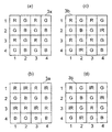
- FIG. 6 is a diagram for explaining the arrangement of color filters of the image sensor, wherein (a) is a diagram showing a conventional arrangement without an infrared filter section, and (b), (c), (d).
- FIG. 4 is a diagram showing an array having an infrared filter section. It is the schematic which shows the imaging device which has the said imaging sensor equally.
- FIG. 3 is a block diagram for explaining signal processing in a signal processing unit of the imaging apparatus. It is a figure for demonstrating the interior process in the signal processing of the said imaging device. It is the schematic which shows the imaging device of the 2nd Embodiment of this invention. It is a figure for demonstrating the arrangement
- FIG. 10 is a diagram of an R signal for explaining the reason why the luminance decreases in the highlight portion. It is a figure of G signal for demonstrating the reason a brightness
- FIG. 10 is a diagram of an R signal for explaining the reason why the luminance decreases in the highlight portion. It is a figure of G signal for demonstrating the reason a brightness
- FIG. 11 is a diagram of an IR signal for explaining the reason why the luminance decreases in the highlight portion. It is a figure which shows the clip level corresponding to each RGB color signal of IR signal.
- FIG. 6 is a diagram for explaining subtraction of clipped IR signals from RGB color signals, where (a) shows the case of the R signal, (b) shows the case of the G signal, and (c ) Is a diagram showing a case of a B signal.
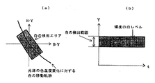
- FIG. 6 is a diagram for explaining white balance processing, where (a) shows a region set to white in the plane of the RY signal and BY signal, and (b) shows white. It is a figure which shows the range of a luminance level.
- FIG. 6 is a diagram for explaining subtraction of clipped IR signals from RGB color signals, where (a) shows the case of the R signal, (b) shows the case of the G signal, and (c ) Is a diagram showing a case of a B signal.
- FIG. 6 is a diagram
- FIG. 6 is a diagram for explaining a method for adjusting the output level of each RGB signal clip after the IR signal is subtracted;
- FIG. 2 is a block diagram illustrating a signal processing unit of the imaging processing apparatus. It is a block diagram which shows the signal processing part as another example same as the above. It is a figure for demonstrating the saturation level of the RGBC color filter of the 7th Embodiment of this invention. It is a figure for demonstrating that the signal level of IR signal calculated
- FIG. 6 is an RGBC signal diagram for explaining the reason why the brightness decreases in the highlight portion. It is a block diagram for demonstrating a separation device equally. It is a block diagram for demonstrating a clip level calculation device same as the above.
- FIG. 2 is a block diagram for explaining an IR signal generation device.
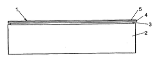
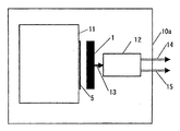
- An image sensor (image sensor) 1 includes, for example, as shown in FIG. 1, a sensor body 2 that is a CCD (Charge Coupled Device) image sensor, and red (corresponding to each pixel of the sensor body 2). R), green (G), blue (B), infrared (IR) regions (filters of each color) arranged in a predetermined arrangement, and a cover glass covering the sensor body 2 and the color filter 3 4 and a DBPF (double band pass filter) 5 formed on the cover glass 4.
- CCD Charge Coupled Device
- the sensor body 2 is a CCD image sensor, and a photodiode as a light receiving element is arranged in each pixel.
- the sensor body 2 may be a CMOS (Complementary Metal Oxide Semiconductor) image sensor instead of the CCD image sensor.
- CMOS Complementary Metal Oxide Semiconductor
- the sensor body 2 is provided with a color filter 3.
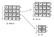
- the color filter 3 is obtained by adding an IR filter to the color filter 3x having three filter parts of R, G, and B arranged in each pixel in the general Bayer arrangement shown in FIG. Yes.
- the basic pattern is composed of 16 color filter sections of 4 rows (horizontal arrangement) ⁇ 4 columns (vertical arrangement).
- the first row is F11, F12, F13, F14
- the second row is F21, F22, F23, F24
- the third row is F31, F32, F33, F34
- the eyes are F41, F42, F43, and F44.
- the Bayer array eight filter units F12, F14, F21, F23, F32, F34, F41, and F43 are G, and four filter units F11, F13, F31, and F33 are R, and F22, Four filter parts F24, F42, and F44 are designated as B.
- the reason why the number of G filter units is twice the number of R and B filter units is based on the fact that human eyes are highly sensitive to green. In addition, even if the lower sensitivity is set to high resolution, it may not be recognized by the human eye, but if the higher sensitivity is set to high resolution, it is more likely to be recognized by the human eye. Be recognized.
- the G filters are arranged in a checkered pattern every other row in the row direction (horizontal direction) and in the column direction (vertical direction). The filter parts are arranged without being adjacent to each other.
- the color filter 3 according to the present embodiment has four Rs by setting four of the eight G filter units in the Bayer array as IR.
- G, 4 B, and 4 IR filters 3 a are included. That is, in the basic arrangement of 4 rows and 4 columns, four types of R, G, B, and IR filter units are arranged four by four, and the same type of filter units are adjacent to each other in the row direction and the column direction.
- the R, G, B, and IR filter units are arranged one by one in each column, and two types of filters of the R, G, B, and IR filter units are arranged every other row. Two parts are arranged respectively.
- filter units F11, F13, F32, and F34 are R
- filter units F12, F14, F31, and F33 are IR
- filter units F21, F23, F42, and F44 are used.
- the number of filter sections is G
- the four filter sections F32, F34, F41, and F42 are B.
- the reduction of the G filter unit may cause the resolution to appear to the human eye to be deteriorated, but each color including IR is evenly arranged to facilitate the interpolation (interpolation) process. . Further, the positions of the respective colors are arranged so as to be shifted by one column in the first, second and third and fourth lines. In other words, the color arrangement is reversed left and right in the first, second and third and fourth lines.
- each color is arranged in each column and two colors are arranged in every other row, so the horizontal direction (horizontal direction) rather than the vertical direction (vertical direction).
- the resolution in the horizontal direction due to the IR filter portion can be suppressed.
- the color filter 3a includes a color filter 3a shown in FIG. 5B that is horizontally reversed, vertically inverted, and 180-degree rotated.
- times may be included. However, those rotated 90 degrees and 270 degrees have higher resolution in the vertical direction than in the horizontal direction.
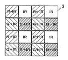
- color filter 3 As in the color filter 3 b shown in FIG. 5C, 2 of the four Bs of the pattern of the color filter 3 x in the Bayer array described above without reducing G that is highly sensitive to humans.
- One may be IR.
- This color filter 3b has a basic arrangement of 4 rows and 4 columns, 8 filter units for G, 4 filter units for R, and B filter among 4 types of filter units of R, G, B, and IR. And two IR filter units are arranged, and the same type of filter units are arranged so as not to be adjacent to each other in the row direction and the column direction.
- the color filter 3b includes a color filter 3b shown in FIG. 5C that is horizontally reversed, vertically inverted, and 180-degree rotated. Moreover, what rotated 90 degree
- the color filter 3c has a basic arrangement of 4 rows and 4 columns, including 8 G filter units, 4 IR filter units, and 4 R filter units of R, G, B, and IR. Two filter units and two B filter units are arranged, and the same type of filter units are arranged so as not to be adjacent to each other in the row direction and the column direction.
- the color filter 3c includes a color filter 3b shown in FIG. 5D that is inverted horizontally, vertically inverted, and rotated 180 times. Moreover, what rotated 90 degree
- a well-known filter can be used for each of the R filter portion, the G filter portion, and the B filter portion of the color filter 3.
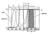
- the transmittance spectra of the R filter unit, the G filter unit, and the B filter unit in the present embodiment are as shown in the graphs of FIGS. 2, 3, and 4. 2, 3 and 4 show the transmittance spectra of the red (R), green (G), blue (B), and infrared (IR) filters of the color filter 3, and the vertical axis. Indicates the transmittance, and the horizontal axis indicates the wavelength.
- the wavelength range in the graph includes a part of the visible light band and the near-infrared band, and shows a wavelength range of 300 nm to 1100 nm, for example.
- the R filter portion has a substantially maximum transmittance at a wavelength of 600 nm, and the long wavelength side has a substantially maximum transmittance even when the wavelength exceeds 1000 nm. It will be maintained.
- the G filter portion has a peak at which the transmittance is maximized at a portion where the wavelength is about 540 nm, as indicated by G (broken line having a wide interval) in the graph, and the transmittance at a portion where the wavelength is about 620 nm on the long wavelength side. There is a part that becomes minimal. Further, the G filter portion tends to rise on the longer wavelength side from the portion where the transmittance is minimized, and the transmittance is substantially maximum at about 850 nm. On the longer wavelength side, the transmittance is substantially maximum even when the wavelength exceeds 1000 nm.
- the filter part of B has a peak where the transmittance is maximized at a part where the wavelength is about 460 nm, as shown in B (dashed broken line) of the graph, and a part of about 630 nm on the long wavelength side thereof, There is a part where the transmittance is minimized. Further, the longer wavelength side tends to increase, and the transmittance is substantially maximized at about 860 nm. On the longer wavelength side, the transmittance is substantially maximized even if it exceeds 1000 nm.
- the IR filter section blocks light on the short wavelength side from about 780 nm, blocks light on the long wavelength side from about 1020 nm, and the portion of about 820 nm to 920 nm has a substantially maximum transmittance.
- each of the R, G, B, and IR filter units is not limited to that shown in FIG. 2 and the like, but the color filter 3 that is currently used generally has a transmittance close to this. It seems to show a spectrum.
- 1 on the horizontal axis indicating the transmittance does not mean that 100% of light is transmitted, but the color filter 3 indicates, for example, the maximum transmittance.
- the cover glass 4 covers and protects the sensor body 2 and the color filter 3.
- the DBPF 5 is an optical filter formed on the cover glass 4.
- the DBPF 5 has a transmission characteristic in the visible light band, a cutoff characteristic in the first wavelength band adjacent to the long wavelength side of the visible light band, and a second wavelength that is a part of the first wavelength band.
- An optical filter having transmission characteristics in a band.
- the DBPF 5 is located at a position slightly apart from the visible light band indicated by DBPF (VR) on the long wavelength side with respect to the visible light band, as indicated by DBPF (solid line) in the graph.
- the transmittance of the two bands of the infrared band (second wavelength band) indicated by DBPF (IR) is high.
- DBPF (VR) as a band having high transmittance in the visible light band has a wavelength band of about 370 nm to 700 nm, for example.
- DBPF (IR) as the second wavelength band having high transmittance on the infrared side is, for example, a band of about 830 nm to 970 nm.
- the relationship between the transmittance spectrum of each filter section of the color filter 3 and the transmittance spectrum of DBPF 5 is defined as follows. That is, DBPF (IR), which is the second wavelength band that transmits infrared light in the transmittance spectrum of DBPF5, has the maximum transmittance of the cheek at all of the R filter unit, the G filter unit, and the B filter unit. 2 is included in the wavelength band A shown in FIG. 2 where the transmittance is substantially the same in each filter unit, and is also included in the wavelength band B that transmits light at the substantially maximum transmittance of the IR filter unit. It has become.
- DBPF IR
- the wavelength band A in which the transmittances of the R, G, and B filter portions are substantially the same is a portion where the transmittance difference of each filter portion is 10% or less.
- the transmittances of the G and B filter units are lower than the R filter unit having the maximum transmittance.
- DBPF5 the difference in transmittance of the R, G, and B filter portions is DBPF (VR), which is a portion with high transmittance in the visible light band, and the second wavelength band in the infrared light band. This corresponds to a portion where the transmittance for substantially blocking the light of DBPF 5 between DBPF (IR) and the portion having a high transmittance is minimal.
- the transmission of light in a portion where the difference in transmittance between the R, G, and B filter portions becomes large is cut, and the transmittance of each filter portion becomes substantially maximum on the longer wavelength side.
- Light is transmitted in the wavelength band A where the transmittance is substantially the same.
- DBPF 5 used in place of the infrared light cut filter has a region that transmits light not only in the visible light band but also in the second wavelength band on the infrared light side. Therefore, in color imaging with visible light, it is affected by the light that has passed through the second wavelength band.
- the second wavelength band has transmittance in each of the R, G, and B filter units. The light of different portions is not transmitted, and only the light in the wavelength band in which the transmittance of each filter unit is substantially maximized and has substantially the same transmittance is transmitted.
- the R filter unit is used in the second wavelength band.
- G filter part, B filter part, IR filter part light passes through in substantially the same manner, and as infrared light, light of substantially the same amount of light in each filter part including IR is image sensor body To the photodiode of the above-mentioned pixel.
- the amount of light that passes through the second wavelength band on the infrared side of the light that passes through the R, G, and B filters is the same as the amount of light that passes through the IR filter section.
- the output signal of the assumed pixel from the sensor body 2 receiving the light transmitted through the R, G, and B filters and the IR filter as described above are passed.
- R, G, and B obtained by cutting off the infrared light that has passed through the R, G, and B filter sections as the difference from the assumed pixel output signal from the sensor body 2 that has received the light as described above.
- the output signal of the visible light portion is the output signal of the visible light portion.
- each pattern of the color filter 3 (3a, 3b, 3c)
- one of the R, G, B, and IR filter sections is arranged in each pixel of the sensor body 2. Therefore, there is a high possibility that the amount of light of each color irradiated to each pixel is different.
- interpolation method for each color of each pixel Luminance is obtained, and the difference between the interpolated R, G, and B luminances of the interpolated pixels and the interpolated IR luminance can be set as the R, G, and B luminances, respectively.
- the image processing method for removing the infrared light component from the luminance of each color of R, G, B is not limited to this, and finally passes through the second wavelength band from each luminance of R, G, B. Any method may be used as long as it can cut the influence of light.
- the DBPF 5 cuts a portion where the transmittance of the R, G, B filter portion on the infrared side is different from 10%, that is, a portion where the transmittance is different from a predetermined ratio. This makes it easy to remove the influence of infrared light.
- the use of the image sensor 1 is to use it as an image sensor in an image pickup apparatus capable of both color photographing and infrared light photographing.
- the transmittance spectrum of DBPF 5 shown in FIG. 3 takes into account the transmittance spectrum of each of the R, G, B, and IR filter sections and the emission spectrum of light for infrared illumination, for example, the infrared LED for illumination. Determined. 3, in addition to the transmittance spectra R, G, B, IR of the filter portions of the same colors as in FIG. 2 and the transmittance spectrum DBPF of DBPF5, an emission spectrum IR-light of LED illumination is shown.
- the second wavelength band indicated by DBPF (IR) which is a part that transmits infrared light of the DBPF shown in FIG. 3, is an R filter unit, a G filter unit, and a B filter. 2 are included in the wavelength band A shown in FIG. 2 where the transmittance is substantially the same in each filter portion, and light is transmitted with the maximum transmittance of the IR filter portion.
- the wavelength band B to be included.
- substantially the entire wavelength band that is the peak of the emission spectrum of infrared illumination included in both the wavelength band A and the wavelength band B described above is included in the DBPF (IR) wavelength band.
- the second wavelength band indicated by DBPF (IR) does not have to be wider than the peak width of the optical spectrum of infrared light illumination when infrared light photography is performed under infrared light illumination instead of nighttime natural light.
- the peak width of the emission spectrum of the infrared light illumination is approximately the same as the peak width having a peak at about 860, for example. You may provide the peak part of the transmittance
- the peak in the emission spectrum of infrared illumination indicated by IR-light is on the short wavelength side of the above-described wavelength band A and wavelength band B, and the second wavelength of DBPF indicated by DBPF (IR)
- the band substantially overlaps the peak of the emission spectrum in the IR-light of the short wavelength side portion of the wavelength band A and the wavelength band B.
- the graph shown in FIG. 4 is similar to the fluff shown in FIG. 3 in that the emission spectrum of infrared illumination is added to the graph shown in FIG. 2 and the infrared side transmittance of the DBPF5 transmittance spectrum is high.
- the second wavelength band indicated by a certain DBPF (IR) is matched with the peak of the emission spectrum indicated by IR-light of the above-mentioned infrared light illumination.
- infrared light illumination having a longer emission spectrum peak wavelength than that shown in FIG. 3 is used, and this peak is included in the above-described wavelength band A and wavelength band B. It exists on the long wavelength side of the wavelength band A and the wavelength band B.
- the second wavelength band indicated by DBPF (IR) of DBPF 5 is provided so as to be substantially umbrella with the peak indicated by IR-light of infrared illumination within the above-mentioned wavelength band A and wavelength band B. .
- the second wavelength band of DBPF 5 may be that shown in any of FIGS. 2, 3, and 4, and the second wavelength band is included in both wavelength band A and wavelength band B described above. It only has to be done. Further, when the wavelength band that is the peak of the emission spectrum of infrared light illumination used for nighttime infrared light photography is determined, the wavelength band is included in both the wavelength band A and the wavelength band B described above. In addition, it is preferable to match the second wavelength band of DBPF 5 with the peak of the emission spectrum of infrared illumination.
- the second wavelength band that transmits light on the infrared side of the DBPF 5 is the infrared side of each of the R, G, B, and IR filter units, and the transmittance of each filter unit is substantially the same.
- the maximum is included in the wavelength band A when the transmittance of each filter part is substantially the same, and is included in the wavelength band B where the transmittance of the IR filter part is substantially maximum.
- the transmittance of each of the R, G, and B filters is substantially maximum only for the R fill portion, and the transmittance of the G and B filter portions is substantially maximum. Due to the absence, the transmittances of the R, G, and B filter portions are not substantially the same, and different portions of light are cut by the DBPF 5.
- each filter part of R, G, B, IR since the light of the second wavelength band is transmitted on the infrared side, the infrared side transmittance in each filter part is substantially the same, If the light in the second wavelength band is irradiated with the same light amount, the transmitted light amounts in the R, G, B, and IR filter units are the same. Thereby, as described above, the color based on the output signal from the pixel corresponding to each of the R, G, and B filter units is corrected, and the influence of the infrared light passing through the second wavelength band of the color at the time of color photographing is performed. It is possible to easily obtain an image in which the above is suppressed.
- the second wavelength band corresponds to the peak of the emission spectrum of the infrared light illumination included in the wavelength band A and the wavelength band B described above, the light of the infrared light illumination can be used efficiently,
- the width of the second wavelength band can be narrowed to reduce the influence of infrared light passing through the second wavelength band during color photography.
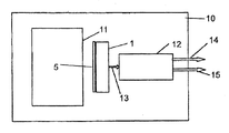
- FIG. 6 shows an imaging apparatus 10 using the imaging sensor 1 of the present embodiment.
- the imaging device 10 processes the imaging lens 11, the imaging sensor 1 including the DBPF 5, and the output signal 13 output from the imaging sensor 1, and performs the above-described interior processing or the second wavelength during color imaging.
- a signal processing unit (signal processing device) 12 that performs image processing for removing the influence of infrared light that has passed through the band, image processing such as gamma correction, white balance, and RGB matrix correction on the image signal is provided.
- a visible color image output signal 14 and an infrared light image output signal 15 can be output from the image processing unit.
- the lens 11 constitutes an optical system that connects an image on the image sensor 1 of the image pickup apparatus 10.
- the lens 11 is composed of a plurality of lenses, for example.
- FIG. 7 is a block diagram showing signal processing in the signal processing unit 12 of the imaging apparatus 10. Output signals from the R, G, B, and IR pixels are sent to the interior processing blocks 21r, 21g, 21b, and 21ir. In each of the interior processing blocks 21r, 21g, 21b, and 21ir, for example, as shown in FIG.
- the infrared light removal signal creation blocks 22r, 22g, 22b, and 22ir in order to remove the influence of the infrared light received from the second wavelength band described above, signals of each color of R, G, and B are used. A signal to be subtracted from is generated from the IR signal.
- the signals created for each of R, G, and B by the infrared light removal signal creation blocks 22r, 22g, and 22b are subtracted from the signals of the R, G, and B colors.
- the IR signal is basically removed from the R, G, and B signals, which facilitates processing.
- the sensitivity differs for each color pixel depending on the characteristics of the filter section of each pixel, and therefore, a signal to be subtracted from each R, G, B signal for each R, G, B image from the IR signal. create.
- the R, G, and B signals are converted into R, G, and B signals using a determinant to correct the colors, and a known RGB matrix process is performed.
- the well-known gamma correction which is the correction for the image output to a known white balance process and a display etc. which makes the output value of each signal of R, G, B become the same is performed.
- a signal of luminance Y is generated by multiplying the R, G, B color signals by coefficients. Also, by dividing the signal of luminance Y from the signal of blue B and red R, the color difference signals of RY and BY are calculated, and Y, RY, and BY signals are output. To do.
- the IR signal is basically output as a monochrome gradation image.
- such an imaging apparatus 10 as described in the above-described imaging sensor 1, it is possible to easily perform image processing for removing the influence of infrared light from a color image, and a visible color image having excellent color reproducibility. Can be obtained. In addition, the development cost of such an imaging apparatus can be reduced.
- the R, G, and B filter units have mutually different transmittances. Since it is physically cut by the DBPF, in the image processing, it is only necessary to perform a process of cutting the IR light at a portion where the transmittance is substantially maximum on the infrared side of each of the R, G, and B filter portions. It will be. In this case, image processing becomes easy, and it becomes possible to obtain color image data having the same color reproducibility as when a conventional infrared light cut filter is used.
- the light that passes through the R, G, and B filter sections and reaches the photodiode is the same as the visible light that has passed through the respective filter sections in the visible light region and the R, G, and B filter sections.
- the infrared light that has passed through the second wavelength band that is the same in the IR filter section. Therefore, for example, the output signal of the IR after the interpolation processing corrected according to the characteristics such as the sensitivity based on the filter unit of each color is subtracted from each output signal after the interpolation processing of the R, G, B of the imaging sensor 1. By doing this, it is possible to obtain color reproducibility close to that when an infrared cut filter is used.
- each filter unit substantially It is difficult to obtain the amount of infrared light that should be cut from the light that has passed through the image, and it is difficult to obtain image data having the same color reproducibility by using image processing as when an infrared light cut filter is used. .
- the image pickup apparatus 10 a is such that the image sensor 1 is not provided with the DBPF 5 but the lens 11 is provided with DPBF.
- the imaging device 10a processes the imaging lens 11 provided with the DBPF 5, the imaging sensor 1, and the output signal 13 output from the imaging sensor 1, and performs the above-described interior processing and the second wavelength during color imaging.
- a signal processing unit 12 that performs image processing for removing the influence of infrared light that has passed through the band, image processing such as gamma correction, white balance, and RGB matrix correction on the image signal.
- a visible color image output signal 14 and an infrared light image output signal 15 can be output from the image processing unit.
- the DBPF 5 and the color filter 3 are the same as the DBPF 5 and the color filter 3 of the first embodiment.
- the transmittance of each of the R, G, B, and IR filter portions of the color filter 3 and the second of the DPBF 5 The relationship of the wavelength band DBPF (IR) is the same as that of the first embodiment. Therefore, unlike the first embodiment, even if the lens 11 is provided with the DBPF 5, the same operational effects as those of the imaging device 10 of the first embodiment can be obtained.
- the DBPF 5 is provided in the optical system of the imaging device 10a, and has a visible light band (DBPF (VR)) and a second wavelength band on the infrared side (DBPF (IR)) with respect to light reaching the imaging sensor 1. So that the light is blocked at the short wavelength side of the visible light band, the long wavelength side of the second wavelength band, and the wavelength band between the visible light band and the second wavelength band. It may be provided anywhere as long as it is.
- the imaging sensor 1 and the imaging apparatus according to the third embodiment are different in the configuration of a part of the color filter 3 and the IR component removal method from the RGB signals.
- the color filter 3 and the IR component removal method will be described below.
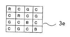
- the color filter 3e (RGBC configuration 1), for example, as shown in FIG. 10, two of the four B of the pattern of the color filter 3x in the Bayer array described above are represented as C. Two of the two R's are C, and four of the eight G's are C. That is, the color filter 3e has a basic arrangement of 4 rows and 4 columns, of 4 types of R, G, B, and C filter units, 4 G filter units, 8 C filter units, Two filter units and two B filter units are arranged, and the same type of filter units are arranged so as not to be adjacent to each other in the row direction and the column direction. Accordingly, the eight C filter units are arranged in a checkered pattern.
- C indicates a transparent state as a clear filter part, and basically has transmission characteristics from the visible light band to the near-infrared wavelength band.
- the visible light band C R + G + B.
- the R, G, and B filter sections have transmission characteristics on the long wavelength side of the visible light band. Even in the C filter section, which is a clear filter section, light is transmitted on the long wavelength side of the visible light band.
- the infrared that transmits the longer wavelength side than the visible light band is limited to the second wavelength band, and R
- the amount of light passing through the G, B, and C filter units and the DBPF 5 is almost the same (approximate) in each of the R, G, B, and C filter units, and in the visible light band, the R, G, B, and C filters
- the transmission characteristics differ according to the wavelength of the part.
- the infrared that transmits longer wavelengths than the visible light band is limited to the second wavelength band, and R, G, B, IR
- the amount of light passing through the filter unit and the DBPF 5 is substantially the same in each of the R, G, B, and IR filter units, and in the visible light band, transmission characteristics corresponding to the wavelengths of the R, G, B, and IR filter units are provided. Different.
- the third embodiment it is possible to perform IR correction of each pixel with high accuracy and to generate a visible image with high color reproducibility.
- it does not include the above-described IR filter unit that has a cutoff characteristic in substantially the entire wavelength range of the visible light band and has a transmission characteristic in the infrared on a longer wavelength side than the visible light band.
- the C filter unit the IR signal can be calculated by the following equation.
- C (W), R, G, B, and IR indicate the level of the output signal from the imaging sensor 1, but C (W), R, G, and B indicate the level of the visible light band. It is assumed that the infrared component is not included.
- IR represents an actual value obtained by measurement or the like
- IR ′ represents a value obtained by calculation.
- the IR transmittance of each filter unit can be approximated by the DBPF 5, and the IR component is obtained as described above. By removing this from the signal of each filter unit, color reproducibility can be improved.
- the amount of light received by the pixel is likely to be saturated and the C filter section reduces the amount of light received in the visible light band, and the infrared wavelength band and visible light band.
- the amount of received light may be lowered over a wavelength band including the above, or the charge accumulated with respect to the amount of received light may be reduced in the element portion constituting the pixel in each pixel. In that case, it is necessary to change the above formula accordingly.
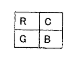
- FIG. 12 shows another arrangement of R, G, B, and C color filters.
- R, G, B, and C are evenly arranged one by one. is there.
- R, G, B Bayer array as shown in FIG. 13
- R and B are arranged one by one and two G are arranged.
- a 2 ⁇ 2 array of R, G, B, and IR color filters in which one of the conventional arrays that does not include C or IR is changed to IR is, as shown in FIG. G, B, and IR are arranged one by one.
- the RGB-C configuration 1 shown in FIG. 10 the RGB-C configuration 2 shown in FIG. 12, the conventional RGB array (Bayer array) shown in FIG. 13, and the RGB-IR array shown in FIG.
- the RGB-C (Configuration 1) sensor has a high luminance resolution due to the checkered arrangement of C, but RGB pixels are sparse,
- the resolution is low and moire tends to occur.
- the resolution required for the color signal is lower than that of the luminance signal, which is 1/2 or less, so that there is no problem.
- the sensitivity is high.
- RGB-C (Configuration 2) has the same luminance resolution and color resolution as the conventional RGB sensor, and has higher sensitivity than the RGB sensor.
- the RGB-IR sensor is provided with an IR that does not have transmission characteristics in the visible light band, so that the sensitivity is lower than that of the RGB sensor, and the luminance resolution is also lower. That is, the color filter having C is more likely to be advantageous in resolution and sensitivity than the color filter having IR of the first embodiment and the second embodiment.
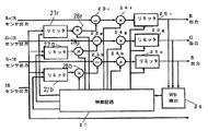
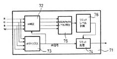
- FIG. 16 is a block diagram showing signal processing in the signal processing unit 12 of FIG.
- the imaging sensor 1 includes the RGB-C sensor 1 including the above-described RGB-C color filter 3e, and also includes a lens 11 and a DBPF 5 that constitute an optical system.
- R + IR, G + IR, B + IR, and C + IR signals are input from the RGB-C sensor 1 to a separation device 51 that performs color separation, IR separation, and IR correction, and R, G, B, W, and IR signals are obtained and output. This process is performed based on the calculation using the above-described equation.
- R, G, B, W, and IR signals output from the separation device 51 R, G, and B signals are sent to the color matrix device 52, where known RGB matrix correction and the like are performed, and RGB signals. Is output. Also.
- the R, G, B, W, and IR signals from the separation device 51 are sent to the luminance generation device 53, and a luminance signal is generated from each signal based on an equation for obtaining the set luminance.
- the RGB signals output from the color matrix device are input to the gamma processing and color difference generation device 54, where known gamma processing is performed, and for example, BY and RY signals are generated as the color difference signals.
- the signals output from the separation device 51 and the RGB-C sensor 1 are reduced in noise after being reduced in noise by the noise reduction device 56 as a signal of a predetermined wavelength band via a BPF (band pass filter) 55.
- the signal is amplified by the enhancement processing device 57 together with the luminance signal output from the generation device 53, and is output as a luminance signal (Y signal) of the luminance / chrominance signal through the gamma processing in the gamma processing device 58.
- the IR signal output from the separation device 51 is output as an IR signal via the enhancement processing device 59 and the gamma processing device 60. In the image signal processing, clip processing described later is performed, and the clip processing will be described later.
- each color of the color filter is generalized, and the color filter of the present invention is not limited to RGB-IR or RGB-C.
- the four color (four types) filter units basically have different transmission characteristics according to the wavelength in the visible light band, and the wavelength band including the second wavelength band of the DBPF described above includes a visible light band.
- a third wavelength band having a transmittance difference of 10% or less with other filter units on the longer wavelength side is provided, and the third wavelength band includes the second wavelength band of DBPF5. ing.
- IR can be separated by designing a color filter under the following conditions in a filter arrangement of four types of pixels.
- the filter arrangement is preferably a 2 ⁇ 2 arrangement, and each of the four types of filter sections A, B, C, and D is provided.
- A, B, C, and D indicate the level of the output signal from the imaging sensor 1 in the visible light band of each filter unit.
- the IR transmittance is substantially constant in the above-described third wavelength bands of the A, B, C, and D filter units.
- the IR transmittance may be approximately an integral multiple of a certain IR transmittance in each of the A, B, C, and D filter units.
- IR transmittance is constant as described above
- IR ′ (Ka (A + IR) + Kb (B + IR) + Kc (C + IR) + Kd (D + IR)) / (Ka + Kb + Kc + Kd)
- C ′ C + IR ⁇ (Ka (A + IR) + Kb (B + IR) + Kc (C + IR) + Kd (D + IR)) / (Ka + Kb + Kc +
- a ' A + IR * KIRa-KIRa (Ka (A + IR * KIRa) + Kb (B + IR * KIRb) + Kc (C + IR * KIRc) + Kd (D + IR * KIRd)) / (Ka * KIRa + Kb * KIRb + Kc * KIRc + Kd * KIRd)
- B ' B + IR * KIRb-KIRb (Ka (A + IR * KIRa) + Kb (B + IR * KIRb) + Kc (C + IR * KIRc) + Kd (D + IR * KIRd)) / (Ka * KIRa + Kb * KIRb + Kc * KIRc + Kd * KIRd)
- C ' C + IR * KIRc-KIRc (Ka (A + IR * KIRa) + Kb (B + IR * KIRb) + Kc (C + IR * KIRc) + Kd (D + IR * KIRd)) / (Ka * KIRa + Kb * KIRb + Kc * KIRc + Kd * KIRd)
- D ' D + IR * KIRd-KIRd (Ka (A + IR * KIRa) + Kb (B + IR * KIRb) + Kc (C + IR * KIRc) + Kd (D + IR * KIRd)) / (Ka * KIRa + Kb * KIRb + Kc * KIRc + Kd * KIRd)
- each filter unit The spectral transmission characteristics of each filter when using DBPF are as shown in FIG.
- the filter unit four types of filter units of R + IR, G + IR, B + IR, and C + IR are used.
- the IR portion is constant or an integer multiple of each other, so that KaA + KbB + KcC + KdD ⁇ 0.
- each filter unit is not limited to R + IR, G + IR, B + IR, and C + IR.
- FIG. 18 shows spectral transmission combining the B filter unit and DBPF5
- FIG. 19 shows spectral transmission combining the G filter unit and DBPF5
- FIG. 20 shows spectral transmission combining the B filter unit and DBPF5.
- FIG. 21 shows the spectral transmission obtained by combining the C (W) filter unit and the DBPF 5.
- Each spectral transmission characteristic is obtained by adding four transmittances of a visible R transmission region, a visible G transmission region, a visible B transmission region, and an IR transmission region, as shown in the above-described equations. . From this, the signal values of each visible R transmission region, visible G transmission region, visible B transmission region, and IR transmission region can be calculated from the values of four or more types of filters. The spectral transmission characteristics are determined based on the above-described equations indicating the branch transmission characteristics of B, C, and D. Six types are determined from combinations of spectral transmission characteristics of two of these filters.
- the imaging sensor 1 that outputs a signal in the visible light band and an infrared signal on the longer wavelength side is mounted on a smartphone or the like, on the smartphone side, a circuit that processes a signal from the imaging sensor 1 is a main circuit.
- the signal is on an SOC (System On Chip) functioning as an arithmetic processing unit
- the RGB signal output from the image sensor includes an IR component as described above, and processing that removes the IR component is required.
- the smartphone needs to be provided with a circuit for performing the IR correction described above. In these cases, when an imaging sensor capable of outputting both visible light and infrared image signals is introduced into a device such as a smartphone, an increase in cost occurs in a portion other than the imaging sensor.
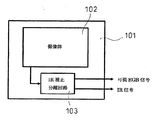
- the imaging sensor 101 includes an imaging unit 102 and an IR correction / separation circuit 103 having substantially the same configuration as the above-described imaging sensor 1.
- a visible RGB signal and an IR signal are output.
- the IR correction / separation circuit 103 includes a circuit that performs processing related to signal level clipping, which will be described later.
- the RGB signal and the IR signal are output, the number of pins of the imaging sensor 101 is increased.
- a serial output standard such as CSI-2, an increase in the number of pins can be suppressed.
- the visible RGB signal is output as a RAW signal output of a RGBG Bayer array image sensor or a YUYV (YCb, YCr) signal.
- the IR signal by outputting the IR signal as a monochromatic signal, simultaneous visible and near-infrared imaging can be utilized by the RGB-IR sensor and the RGB-C sensor without changing the SOC of the smartphone or the future phone.
- the structure of the image sensor 101 is, for example, a stacked stack structure as shown in FIG. 23.
- an integrated circuit chip constituting the IR correction / separation circuit 103 is mounted on one substrate 110, and A chip that constitutes the imaging unit 102 is placed over the top.
- a cover glass 111 is disposed on the imaging unit 102.
- Solder balls 115 are disposed on the bottom surface of the substrate 110.
- the structure of the image sensor 101 is such that two substrates 110 are stacked one above the other at an interval in the vertical direction, and the chip of the IR correction / separation circuit 103 is placed on the lower substrate 110.
- the chip of the imaging unit 102 may be arranged on the upper substrate 110, and the cover glass 111 may be arranged thereon.
- the IR correction / separation circuit 103 and the imaging unit 102 can be stacked one above the other as described above to form a single package sensor. Even with this method, the image sensor 101 incorporating the IR correction / separation circuit can be realized with a single package. In this manner, a small sensor that can simultaneously capture small visible / near infrared light and can be used in a smartphone or the like can be realized without including a correction separation circuit.
- a smartphone has functions such as biometric authentication such as iris authentication and 3D capture using an IR sensor, and can capture a moving image / still image with a single sensor.
- FIG. 25 shows a schematic diagram of signal output similar to the RGB Bayer arrangement by IR correction + interpolation.
- R / IR and G / B are output line-sequentially with R, IR, R, IR,... / G, B, G, B,.
- IR correction / IR separation is performed, and the position of the IR pixel is interpolated from the neighboring G signal to generate a G ′ signal, and R, G ′, R, G ′,... / G, B , G, B,..., And outputs visible R / G ′ and G / B signals and separated IR signals.
- the signal processing side can perform processing using the same signal processing circuit.
- the signal processing unit can also perform processing by normal monochrome signal processing.
- the RGB-IR sensor has been described. Even in the visible / near-infrared simultaneous imaging using the RGB-C sensor, an IR correction / separation circuit is incorporated in the sensor, and the conventional RGB Bayer array is used. A similar effect can be obtained by configuring the sensor output format to output a visible signal and an IR signal.
- the imaging apparatus 10 processes a lens 11 that is an optical system for photographing, an imaging sensor 1 that includes a DBPF 5, and an output signal 13 that is output from the imaging sensor 1.
- the image processing includes image processing such as the above-described interior processing, image processing that removes the influence of infrared light that has passed through the second wavelength band during color shooting, gamma correction, white balance, and RGB matrix correction.
- a signal processing unit signal processing device: subtraction control device
- the signal processing unit 12 can output a visible color image output signal 14 (visible image signal) and an infrared light image output signal 15 (infrared image signal).
- the lens 11 constitutes an optical system that connects an image on the image sensor 1 of the image pickup apparatus 10.
- the lens 11 is composed of a plurality of lenses, for example.
- the imaging sensor (image sensor) 1 includes a sensor body 2 that is a CCD (Charge Coupled Device) image sensor, and red (R) and green (corresponding to each pixel of the sensor body 2). G), blue (B), infrared (IR) regions (filters of each color) arranged in a predetermined arrangement, a color filter 3, a cover glass 4 covering the sensor body 2 and the color filter 3, and a cover glass 4 and a DBPF (double band pass filter) 5 formed on the substrate 4.
- CCD Charge Coupled Device
- the sensor body 2 is a CCD image sensor, and a photodiode as a light receiving element is arranged in each pixel.
- the sensor body 2 may be a CMOS (Complementary Metal Oxide Semiconductor) image sensor instead of the CCD image sensor.
- CMOS Complementary Metal Oxide Semiconductor
- the sensor body 2 is provided with a color filter 3.
- a Bayer array color filter that has red R, green G, and blue B regions but no infrared IR region has 16 regions of 4 ⁇ 4 in length, which is a basic pattern. Each region is a G region, four regions are R, and four regions are B.
- the color filter 3 of the present embodiment four of the eight G regions in the Bayer array are IR regions, so that four Rs are obtained.
- G is 4
- B is 4
- IR is 4.
- the color filter including the IR region is not limited to the color filter 3 illustrated in FIG. 28, and various color filters can be used.
- Each of the RGB regions is a general RGB filter, but has a transmittance peak in the wavelength range of each color and transparency in the near-infrared wavelength region.
- the R region was R + IR
- the green region was G + IR
- the blue region was B + IR.
- the transmittance spectrum of the R region, the G region, and the B region in the present embodiment is as shown in the graph of FIG. That is, the transmittance spectrum of each of the red (R), green (G), blue (B), and infrared (IR) filters of the color filter 3 is shown, the vertical axis indicates the transmittance, and the horizontal axis indicates the transmittance. It is a wavelength.
- the wavelength range in the graph includes a part of the visible light band and the near-infrared band, and shows a wavelength range of 300 nm to 1100 nm, for example.
- the R region has a substantially maximum transmittance at a wavelength of 600 nm, and the long wavelength side maintains a substantially maximum transmittance even when the wavelength exceeds 1000 nm. It will be in the state.
- the G region has a peak at which the transmittance is maximized at a portion where the wavelength is about 540 nm, as shown by G (broken line having a wide interval) in the graph, and the transmittance is minimized at a portion where the wavelength is about 620 nm. There is a part that becomes.
- the longer wavelength side tends to increase from the portion where the transmittance is minimized, and the transmittance is substantially maximum at about 850 nm.
- the transmittance is substantially maximum even when the wavelength exceeds 1000 nm.
- the region B has a peak at which the transmittance is maximized at a portion where the wavelength is about 460 nm, as shown by B (dashed broken line) in the graph, and is transmitted at a portion around 630 nm on the long wavelength side. There is a part where the rate is minimal. Further, the longer wavelength side tends to increase, and the transmittance is substantially maximized at about 860 nm. On the longer wavelength side, the transmittance is substantially maximized even if it exceeds 1000 nm. In the IR region, light on the short wavelength side from about 780 nm is blocked, light on the long wavelength side from about 1020 nm is blocked, and the transmittance of the portion of about 820 nm to 920 nm is substantially maximum.
- the transmittance spectrum in each of the R, G, B, and IR regions is not limited to that shown in FIG. 29.
- the color filter 3 that is currently used generally has a transmittance spectrum close to this. It seems to show. Note that 1 on the vertical axis indicating the transmittance does not mean that 100% of the light is transmitted, and the color filter 3 indicates, for example, the maximum transmittance.
- the cover glass 4 covers and protects the sensor body 2 and the color filter 3.
- the DBPF 5 is an optical filter formed on the cover glass 4.
- the DBPF 5 has a transmission characteristic in the visible light band, a cutoff characteristic in the first wavelength band adjacent to the long wavelength side of the visible light band, and a second wavelength that is a part of the first wavelength band.
- the arrangement position of the DBPF 5 is not limited to the cover glass 4, and may be arranged at another location of the imaging sensor 1. Further, the arrangement position of the DBPF 5 is not limited to the image sensor 1 and may be arranged in an optical system that includes the lens 11 and forms an image on the image sensor 1.
- the DBPF 5 has a visible light band indicated by DBPF (VR) as shown by a DBPF (solid line) in the graph, and a DBPF at a position slightly distant from the visible light band on the long wavelength side.
- the transmittance of two bands of the infrared band (second wavelength band) indicated by (IR) is high.
- DBPF (VR) as a band having a high transmittance in the visible light band has a wavelength band of about 370 nm to 700 nm, for example.
- DBPF (IR) as the second wavelength band having a high transmittance on the infrared side is, for example, a band of about 830 nm to 970 nm.
- the relationship between the transmittance spectrum of each region of the color filter 3 and the transmittance spectrum of DBPF 5 is defined as follows. That is, DBPF (IR), which is the second wavelength band that transmits infrared light of the transmittance spectrum of DBPF5, has the cheek maximum transmittance in all of the R region, the G region, and the B region. It is included in the wavelength band A shown in FIG. 29 in which the transmittance is substantially the same in the region, and is also included in the wavelength band B that transmits light with the substantially maximum transmittance in the IR region.
- DBPF IR
- the wavelength band A in which the transmittance in each of the R, G, and B regions is substantially the same is a portion where the transmittance difference in each region is 10% or less.
- the transmittance of the G and B regions is lower than the R region where the transmittance is substantially maximum.
- DBPF5 the portion where the transmittance of each region of R, G, and B is different is DBPF (VR) which is a portion where the transmittance in the visible light band is high, and the second wavelength band in the infrared light band.
- DBPF 5 used in place of the infrared light cut filter has a region that transmits light not only in the visible light band but also in the second wavelength band on the infrared light side. Therefore, in color imaging with visible light, it is affected by light that has passed through the second wavelength band, but the second wavelength band has different transmittances in the R, G, and B regions as described above. A portion of light is not transmitted, and only the light in the wavelength band in which the transmittance of each region is substantially maximized and becomes substantially the same transmittance is transmitted.
- the amount of light that passes through the second wavelength band on the infrared side of the light that passes through the R, G, and B filters is the same as the amount of light that passes through the IR region.
- the output signal of the assumed pixel from the sensor body 2 receiving the light transmitted through the R, G, and B filters and the IR filter as described above are passed.
- the difference from the output signal of the pixel assumed as described above from the sensor main body 2 that has received the light is that of each of R, G, and B obtained by cutting the infrared light that has passed through the R, G, and B regions. It becomes the output signal of the visible light part.
- any one region of R, G, B, IR is arranged for each pixel of the sensor body 2. Since the light quantity of each color light irradiated to each pixel is likely to be different, for example, the brightness of each color of each pixel by using a well-known interpolation method (interpolation method) in each pixel. And the difference between the R, G, and B luminances of each interpolated pixel and the interpolated IR luminance can be set as the R, G, and B luminances, respectively.
- the image processing method for removing the infrared light component from the luminance of each color of R, G, B is not limited to this, and finally passes through the second wavelength band from each luminance of R, G, B. Any method may be used as long as it can cut the influence of light.
- the DBPF 5 cuts a portion where the transmittance of the R, G, B region on the infrared side is different from 10%, that is, a portion where the transmittance is different from a predetermined ratio. Processing that removes the influence of infrared light becomes easy.
- the use of the image sensor 1 is to use it as an image sensor in an image pickup apparatus capable of both color photographing and infrared light photographing.
- the transmittance spectrum of DBPF 5 shown in FIG. 29 takes into account the transmittance spectrum of each region of R, G, B, and IR and the emission spectrum of light for infrared light illumination, for example, the infrared light LED for illumination. decide.
- the second wavelength band that transmits light on the infrared side of the DBPF 5 is the infrared side of each of the R, G, B, and IR regions, and the transmittance of each region is substantially maximum.
- the transmittance of each of the R, G, and B filters is substantially maximum only for the fill portion of R, and the transmittance of the G and B regions is not substantially maximum.
- the transmittances of the R, G, and B regions are not substantially the same, but different portions of light are cut by the DBPF 5.
- the second wavelength band corresponds to the peak of the emission spectrum of the infrared light illumination included in the wavelength band A and the wavelength band B described above, the light of the infrared light illumination can be used efficiently,
- the width of the second wavelength band can be narrowed to reduce the influence of infrared light passing through the second wavelength band during color photography.
- the DBPF 5 it is possible to perform highly accurate correction by subtracting the value of each IR signal from the value of each RGB signal of the imaging sensor 1.
- the signal processing unit 12 an imaging processing method in the imaging apparatus will be described.
- the light receiving components of the pixels of each color of the image sensor 1 are in a state in which an IR component is added to the components of each color as shown below.
- IR correction is performed by removing the IR component from the light receiving components of the RGB pixels excluding the IR pixels.
- the IR component that passes through the DBPF 5 and passes through the color filter can be excluded from each color region other than the IR of the color filter.
- the R pixel, the G pixel, and the B pixel have different sensitivities to each light source, and each pixel of the image sensor 1 has a dynamic range, and charges that exceed the dynamic range cannot be read out.
- the output is clipped and capped. That is, when the input light exceeds the dynamic range, the output signal is clipped and cut off.
- errors occur in the corrected R signal, G signal, and B signal, causing problems such as unnatural luminance level (the luminance of the highlight portion decreases) and coloring in highlights. .
- FIG. 30 to 32 are diagrams for explaining a problem when the IR component is subtracted from each color component in a state where the dynamic range is exceeded.
- FIG. 30 shows the case of R
- FIG. And FIG. 32 shows the case of B.
- the vertical axis represents the output level of the signal from each color pixel of the image sensor 1.
- the horizontal axis indicates the time lapse of the output level of one pixel of the image sensor 1, or the position on the pixel column (for example, the position of each pixel on the Y axis).
- the horizontal axis is the pixel position on the Y axis.
- the graph shows the change in the output level of the signal depending on the position on the Y axis in each pixel of each color.
- FIG. 33 shows the output level of the IR signal for each color shown in FIGS. 30 to 32, and the position of each pixel on the Y axis as in the case of each RGB pixel in each graph described above. Indicates the output level.
- the upper graph shown in each of FIGS. 30 to 32 shows the output level of the signal in the state where the dynamic range is exceeded with the difference in the position on the Y axis, that is, the output level of the signal of each pixel is As the position on the Y-axis changes to the right, it rises and then descends. In RGB except IR, the clipped state exceeds the dynamic range.
- Each pixel of the image sensor 1 can read the charge only up to the pixel saturation level, and the output level is clipped without reading the charge above the pixel saturation level.
- each RGB pixel signal since the output level of each RGB pixel signal includes the output level of the IR signal, it becomes R + IR, G + IR, and B + IR, respectively, and the RGB output level is RGB from the output level of the IR signal. It is higher by a single output level not including IR. Therefore, IR pixels do not exceed the dynamic range, and RGB easily exceeds the dynamic range.
- a graph indicated by a dotted line exceeding the pixel saturation level indicates an output level when not clipped.
- the lower graphs shown in FIGS. 30 to 32 show the case where the output level of IR is subtracted from the output level including the upper IR.
- the upwardly convex portion indicates a case where the output level of the IR signal is subtracted from the output level of each of the RGB signals when not clipped as indicated by the dotted line.
- the output level of the IR which has a mountain shape with a difference in position, is subtracted upward.
- the lower graph becomes a state indicated by the lower graph.
- the output level should be a mountain-like output level where the output level at the center of each pixel in a row becomes higher, but the original output level is clipped beyond the dynamic range as described above, and the pixel saturation level is horizontal.
- the output level of the image signal of the pixel of each color reaches its peak, but at that time IR is still lower than the pixel saturation level, and the brightness is exceeded after other colors exceed the pixel saturation level.
- the higher the value the higher the IR output level. That is, even if the luminance is further increased, the output level of each RGB pixel signal is not increased due to clipping, but the IR output signal subtracted from these is increased. Therefore, the output level obtained by subtracting the IR output level from the RGB output levels decreases as the luminance increases. As a result, the output level drops in the portion where the output level should be the highest, and the brightness drops in the highlight portion. In addition, the portion where all the RGB output levels exceed the pixel saturation level should be white, but there is a difference in the output level when convex downward in each RGB, and the highlight portion does not become white. It will be in a colored state.
- the output level of the IR signal when the output level of the IR signal is subtracted from the output level of the RGB pixel signal, the output level of the RGB pixel signal exceeds the dynamic range, and is clipped at the pixel saturation level. Subtract after lowering the output level of IR to be subtracted. That is, in the value of the output level of the IR signal subtracted from each output level of RGB, FIG. As shown in FIG. 34, even if the output level of the IR signal subtracted from the output level of each RGB pixel signal does not exceed the dynamic range and is below the pixel saturation level, the output level is clipped. As described above, a limit value is set corresponding to each RGB signal (each component), and the output level that is equal to or higher than the limit value is clipped (limited so as to reach a peak) with the set limit value. State.
- the signal saturation level that occurs after subtracting the IR signal of each RGB signal is less than the pixel saturation level because the limit value of the IR signal is subtracted from the pixel saturation level when each RGB signal exceeds the dynamic range. It becomes a low level. Further, the signal saturation level of each RGB signal after the IR signal subtraction differs for each color as described later. Note that the position where the output level of the IR signal shown in FIG. 34 is clipped (IR signal limit value) differs for each RGB signal to be subtracted and changes depending on the situation.
- the limit value (clip level) of the output level of the IR signal when correcting each RGB signal depends on the spectral sensitivity of the image sensor 1, the color temperature of the light source, and the type of light source corresponding to each color of RGB.
- the appropriate clip level varies. This level is difficult to obtain uniformly by calculation, but can be determined by measuring the output level of each RGB signal and the output level of the IR signal output from the sensor for each light source (color temperature).
- the spectral sensitivity of the image sensor 1 is determined by the image sensor 1.
- the color temperature is determined to some extent depending on the type of light source. Therefore, it is necessary to obtain the limit value of the IR signal value corresponding to each RGB signal to which the IR output level is clipped, based on the color temperature.
- the level of each RGB signal changes due to the change in the color temperature of the light source. For example, For light sources with a low color temperature, the R signal increases and the B signal decreases. For a light source having a high color temperature, the B signal increases and the R signal decreases. As a result, when the color temperature is low, the image becomes reddish, and when the color temperature is high, the image becomes bluish. For this reason, the color reproducibility changes depending on the color temperature change of the light source. In order to stabilize this color reproducibility, white balance processing (WB) is performed to keep the RGB signal levels constant.
- WB white balance processing
- the white balance processing is performed by measuring the color temperature of the light source from the color signal and adjusting the gain of each RGB color signal.
- a method of performing white balance detection from an image signal and controlling based on the detection result is common.
- an RGB gain adjustment circuit (included in the control circuit 21 in FIG. 38) and a white balance detection circuit 26 (shown in FIG. 38) constitute a feedback control loop.
- -Y signal, BY signal, or R, G, B signals are integrated.
- control is performed so that these integral values become 0.
- the integral values are made equal. Control the gain of each RGB signal.
- the ratio of each of the R signal, the G signal, and the B signal can be obtained from the gain of each RGB signal, which is information for determining the color temperature of the light source. Based on this information, the limit value (clip level) for each RGB signal of the IR signal at the time of IR correction is determined.
- the component method of the video signal includes an RGB method using RGB corresponding to the three primary colors as a component and a color difference method using a luminance-color difference converted from RGB into a luminance signal and a color difference signal.
- a method using Y, Cb and Cr, a method using Y, Pb and Pr are known.
- Y is luminance
- Cb and Pb are (B (blue) -Y (luminance)) multiplied by a coefficient
- Cr and Pr are coefficients (R (red)-Y (luminance)). Multiplication is performed.
- Cb and Pb are BY signals
- Cr and Pr are RY signals.
- Y, Cb, and Cr are expressed by the following formulas for R, G, and B.
- Y 0.299 * R + 0.587 * G + 0.114 *
- the color difference method reconstructs an RGB signal into a component that represents brightness (luminance) and a component that represents the difference between two color signals and the luminance signal (color difference).
- the processing amount becomes 2/3 compared with RGB.
- the white balance detection is performed in this region by setting a region considered white and detecting the set white region. That is, when the BY signal and the RY signal of the color difference signal of each pixel in the region considered to be white are integrated, the BY signal and the R ⁇ signal are set so that the integrated value becomes zero. Adjust the gain of the Y signal. Alternatively, the gains of the R, G, and B signals are adjusted so that the values obtained by integrating the RGB signals are equal to each other.
- FIGS. An example of a region considered white in white balance detection is shown in FIGS.
- a white detection area is set in the vicinity of the movement locus due to the color temperature of the point that becomes white.
- a white detection range (for example, 70% or more and less than 105% of the white level) is set with respect to the luminance signal level.
- the color difference method when the color difference signal is in the white detection area and the luminance signal is in the white detection range, the pixel is in the white area, and R, G of the pixels in this area , B signals or color difference type BY signals and RY signals are integrated. Alternatively, the gain of each R, G, B signal is adjusted so that the integral values of R, G, B are equal.
- the limit value of the IR signal subtracted from the R (R + IR), G (G + IR), and B (B + IR) signals is the pixel saturation of the R (R + IR), G (G + IR), and B (B + IR) color signals. This value is the upper limit when the value of the IR signal is subtracted from each color signal when the level exceeds the level and clipping is performed at the pixel saturation level.
- the limit value (clip level) corresponding to each RGB signal of the IR signal is such that the saturation level of the pixel is Lsat, and when white is imaged at a certain color temperature, the ratio of the R signal to the IR signal is Kr.
- the limit value (clip level) of the IR signal in the R signal is Lclip-R, it is expressed by the following equation.
- the ratio of the G signal to the IR signal is Kg
- the ratio of the B signal to the IR signal is Kb
- the limit value (clip level) of the IR signal in the G signal is Lclip-G.
- Lclip-G Lsat / (1 + Kg)
- Lclip-B Lsat / (1 + Kb) It becomes.
- Kg / r (R signal gain) / (G signal gain)
- Kb / r (R signal gain) / (B signal gain)
- Kg Kr x Kg / r
- Kb Kr ⁇ Kb / r
- Lclip-G Lsat / (1 + Kr ⁇ Kg / r)
- Lclip-B Lsat / (1 + Kr ⁇ Kb / r)
- Kr with respect to Kb / r is measured and recorded in advance in a memory or the like, so that Kb / r and this Kb / r are obtained based on the gain obtained by white balance detection and the above formula.
- the clip level of the IR signal for color correction can be determined from Kr.
- the vertical axis represents the output level when the IR signal is subtracted from the RGB (R + IR, G + IR, B + IR) signals
- the horizontal axis represents, for example, the position of the pixel on the image sensor 1 in the Y-axis direction. Or the time passage of one pixel is shown.
- the RGB color signals when the RGB color signals have reached the pixel saturation level, the color temperature of the light source does not change, and the RGB clip levels (limit values) obtained as described above are constant.
- each RGB signal When the IR signal limited (clipped) by the limit value (clip level) is subtracted from each RGB signal at the pixel saturation level, each RGB signal has a constant pixel saturation level and corresponds to RGB Since each limit value of the IR signal is constant, the RGB signal after subtraction is in a constant state, that is, a constant state at the signal saturation level. However, as shown in FIG. 37, the signal saturation level is different for RGB, and as it is, white is not white because the output level of the RGB signal is different in the highlight portion. Therefore, the signal saturation level of the R signal having the lowest signal saturation level is set to the RGB clip level common to the RGB signals (R signal saturation level), and the signal saturation levels of the RGB signals are adjusted to the common RGB clip level.
- the signal saturation level ( Clip level). Since the R signal has the lowest signal saturation level of each RGB signal after subtracting the IR signal, the signal saturation level and B of the G signal after subtracting the IR signal are based on the R signal as described above. As shown in FIGS. 37 (b) and 37 (c), the signal saturation level of the signal is lowered in accordance with the RGB clip level equal to the signal saturation level of the R signal, so that the RGB signals after the IR signal subtraction is performed. Adjust the signal saturation level. Thereby, the high level of each signal in a highlight part becomes the same, and coloring of a highlight can be prevented.
- the IR signal is clipped and then subtracted from the R signal, G signal, and B signal.
- the IR signal is a level at which the R signal, G signal, and B signal are saturated. (IR signal clipping level) or more, the IR signal may be subtracted from the R, G, and B signals after the gain is lowered by a multiplier. In this way, by configuring so as to suppress the subtraction amount, unnaturalness of luminance gradation of the R signal, the G signal, and the B signal in the highlight portion may be prevented.
- FIG. 38 is a block diagram showing signal processing in the signal processing unit 12 (illustrated in FIG. 26) of the imaging apparatus 10 (illustrated in FIG. 26). If the output signals of the R, G, B, and IR pixels from the image sensor 1 (input signals from the image sensor 1 in this signal processing) are usually RAW outputs, R, G, B, and IR are lines. Since the signals are output sequentially or dot-sequentially, for example, a synchronizing circuit (not shown) for each color signal is provided at the input portion of the RAW signal from the image sensor 1.
- the signal processing unit 12 includes synchronization circuits for R + IR, G + IR, B + IR, and IR sensor outputs (not shown), and the R + IR, G + IR, B + IR, and IR sensor outputs of FIG. It is a signal after passing.
- the signal processing unit 12 outputs the IR signal subtracted from the RGB signal from the limiters 20r, 20g, and 20b and the limiters 20r, 20g, and 20b for clipping at the clip level (limit value) determined for each RGB.
- Multipliers 22r, 22g, and 22b for multiplying the IR signal by a correction value and the clipped IR signals output from the multipliers 22r, 22g, and 22b are subtracted from the R + IR, G + IR, and B + IR signals.
- the signal processing unit 12 includes a control circuit 21 that calculates and outputs the clip level (limit value) of the IR signal for each RGB signal in the limiters 20r, 20g, and 20b.
- the control circuit 21 outputs correction values to the multipliers 22r, 22g, and 22b, and outputs RGB gains calculated for white balance to the multipliers 24r, 24g, and 24b, and the limiters 25r, 25g, and 25b.
- the signal processing unit also includes a white balance detection circuit 26 for obtaining a white balance gain from the RGB output signals from the signal processing unit 12.
- IR signals as IR sensor outputs are respectively sent to an R limiter 20r, a G limiter 20g, and a B limiter 20b provided in the signal processing unit 12, and for IR signals set for each color as described above. Clipped with the limit value (clip level).
- the R limiters 20r, G corresponding to the red clip level Lclip-R, the green clip level Lclip-G, and the blue clip level Lclip-B of the IR signal calculated by the control circuit 21, respectively. It is output to the limiter 20g for B and the limiter 20b for B, and becomes the limit value of each of the limiter 20r for R, the limiter 20g for G, and the limiter 20b for B. Thereby, the output level exceeding the clip level (limit value) is clipped at the clip level by the limiters 20r, 20g, and 20b.
- the values output from the R limiter 20r, the G limiter 20g, and the B limiter 20b are IR signals that are subtracted from the RGB signals.
- the IR signals are multiplied by multipliers 22r and 22g. , 22b is multiplied by the correction value output from the control circuit 21.
- the IR component included in the R pixel, G pixel, and B pixel is substantially the same level as that of the IR pixel.
- the aperture difference between the R pixel, the G pixel, and the B pixel, or the amplifier in the sensor There may be some error in the signal level due to variations in gain. That is, the values output from the limiters 20r, 20g, and 20b tend to be slightly larger than the necessary values, for example, and the multipliers 22r, 22g, and 22b multiply the correction values corresponding to the RGB signals. To correct.
- the subtractors 23r, 23g, and 23b subtract the IR signals corresponding to RGB that have been clipped and corrected in this way from the R + IR, G + IR, and B + IR signals.
- Each multiplier 24r, 24g, 24b multiplies the signal output from each subtractor 23r, 23g, 23b by each gain of RGB calculated by the white balance processing to obtain white balance.
- the RGB gains calculated by the control circuit 21 based on the RGB signals detected by the white balance detection circuit 26 are input to the multipliers 24r, 24g, and 24b.
- the RGB signals output from the multipliers 24r, 24g, and 24b are clipped by subtracting the clipped IR signal.
- the signal saturation level is a value obtained by subtracting the limit value from the pixel saturation level. Clipped with. If the signal saturation levels of these RGB signals are different, the highlight portion is colored. Therefore, the limiters 25r, 25g, and 25b are the same for each RGB signal in order to match the RGB signal saturation levels.
- the limit value is set so as to be the RGB clip level.
- the signal saturation level of the R signal is set to the RGB clip level as a limit value, and the clip levels of the G signal and the B signal are matched.
- the signal processing as described above will be described by taking an R (R + IR) signal as an example.
- the R signal output from the imaging sensor 1 is interpolated by a synchronization circuit and is used as an R signal for every pixel used as an image by the imaging sensor 1.
- the G signal, the B signal, and the IR signal are processed by the synchronization circuit, and are converted into the G signal, the B signal, and the IR signal for every pixel used as an image.
- the IR signal is sent to the limiter 20r.
- the limiter 20r outputs Lclip-R, which is the limit value of the IR signal for the R signal calculated by the control circuit 21 as described above, and this becomes the limit value of the limiter 20r. Therefore, the IR signal that has passed through the limiter 20r is clipped so as to reach the limit value. That is, the output level of the IR signal exceeding the limit value becomes the limit value.
- the IR signal clipped with the limit value in this way is sent to the multiplier 22r, multiplied by the correction value calculated (or stored) by the control circuit 21 and corrected, and then sent to the subtractor 23r. It is done.
- the subtractor 23r receives the above-described synchronized R signal, and the IR signal that is limited and corrected as described above, and the value of the IR signal is subtracted from the R signal.
- the R signal from which the IR signal has been subtracted is sent to the multiplier 24r.
- the multiplier 24r receives the R signal and the gain of the R signal obtained by the white balance detection circuit 26 and the control circuit 21, and multiplies the R signal by the gain.
- the R signal subjected to the white balance processing is output from the multiplier 24r.
- This R signal is input to the limiter 25r.
- the RGB clip level described above is sent from the control circuit 21 to the limiter 25r, which is set as a limit value, and the R signal exceeding the RGB clip level is clipped.
- the RGB clip level is equal to the R signal saturation level, and the R signal from which the IR signal has been subtracted is already clipped at the R signal saturation level.
- the process of 25r is not necessarily required.
- the G signal and the B signal are clipped at the RGB clip level by the limiters 25g and 25b with the RGB clip level equal to the R signal saturation level as a limit value.
- the G signal and the B signal are processed, and the processed RGB signals are output as an output signal 14 of a color image of visible light as shown in FIG.
- the IR signal is output as an infrared image output signal 15 after passing through a synchronization circuit.
- the IR signal output as the infrared image signal is not limited by the above limit value.
- each RGB signal after the IR signal is subtracted after the white balance multipliers 24r, 24g, and 24b in the block diagram of FIG.
- limiters 25r, 25g, and 25b for adjusting the signal saturation level are arranged, in FIG. 39, limiters 25r, 25g, and 25b for adjusting the clip level of each RGB signal after the IR signal is subtracted. Is followed by white balance multipliers 24r, 24g, and 24b.
- DBPF5 DBPF5
- the camera imaging device
- each RGB signal includes an IR component, whereas the IR signal includes only the IR component. Therefore, even if each RGB signal is saturated, the IR signal is saturated. do not do.
- the RGB component whose level increases even after the RGB signal is saturated, the RGB component is saturated as described above, and then the IR component is removed to lower the saturation level or lower. In particular, as the amount of IR light increases, the RGB values after saturation become lower.
- C R + G + B in the visible light band. Therefore, when the range is adjusted to RGB, the C pixel reaches a saturation level as shown in FIG. become.
- the signal level reaches the peak at the saturation level for C.
- the IR component can be increased even after C reaches the saturation level, and after C is saturated, IR ′> IR as shown in FIG. As shown in FIG. 42, the signal level decreases as the actual light amount level increases. Further, since the RGB signal levels other than C are also IR '> IR after C is saturated, the signal level may decrease as the actual light quantity level increases, although not as high as C.
- clipping is performed so that each signal does not exceed a predetermined value, and an IR signal is separated from each RGB signal.
- R / G / B / W / IR signal level is detected.
- the clip level is obtained by R, G, B, and W as follows.
- (W clip level) (calculated from the saturation level of W pixel (C pixel))
- (R clip level) (W clip level) (R level + IR level) / (W level + IR level)
- G clip level) (W clip level) (G level + IR level) / (W level + IR level)
- B clip level) (W clip level) (B level + IR level) / (W level + IR level)
- the level of the W clip is calculated based on a saturation level at which the signal level reaches a peak when the W signal level is detected and does not increase any more.
- Each RGB clip level is calculated by the above formula, and the clip level is calculated when the W level reaches the saturation level.
- the above-described separation device 51 is a block diagram as shown in FIG.
- the R, G, B, and W signal levels of each pixel are separated by the color separation device 61 by interpolation or the like and sent to the level detection / clip level calculation device 63 and the clip processing device 62.
- the level detection / clip level calculation device 63 calculates R, G, B, and W clip levels based on the above formula and the detected levels of R, G, B, and W.
- the R, G, B, and W clip levels calculated by the clip level calculation device 63 are sent to the clip processing device 62, and the R, G, B, and W signal levels input to the clip processing device 62 are clip levels. If it exceeds, clipping is performed.
- the R, G, B, and W signal levels output from the clip processing device 62 are input to the IR correction / IR generation device 64.
- the IR correction / IR generation device 64 removes the IR signal from the R, G, B, and W signals and generates an IR signal.
- the clip level calculation device 63 obtains the IR signal level by the IR matrix device 66 based on the R, G, B, and W signal levels separated by the color separation device 61, and performs IR correction.
- the R, G, B, and W signal levels including the IR signal and the IR component are input to the device 67, and IR correction is performed to remove the IR signal level from the R, G, B, and W signal levels.
- An IR signal level is input from the IR matrix device 66 to the level detection device 68, and R, G, B, and W signal levels from which IR components are removed are input from the IR correction device 67.
- the R, G, B, W, and IR signal levels detected by the level detection device 68 are input to the clip level calculation device 69, and the clip level calculation device 69 outputs the R, G, B, and W signals as described above.
- the clip level for each signal level is calculated. Based on the R, G, B, and W clip levels obtained in this way, the clip processing device 62 shown in FIG. 45 when the R, G, B, and W signal levels exceed the clip level. As described above, each signal level reaches its peak at the clip level.
- the IR component is obtained and the R, G, B, and W signals including the IR component are obtained in the same manner as in the third embodiment. From the IR component.
- the IR signal obtained by calculation is also clipped at the IR signal level when W becomes the saturation level and reaches a peak state.
- the clip level remains after the IR component is removed.
- the luminance signal obtained from the R, G, B, and W signal levels is also clipped. Therefore, by using a modification of the separation device 51 that performs color separation, IR separation, and IR correction as shown in FIG. 48, the luminance level is prevented from being clipped, and even after the W pixel reaches the saturation level. It is possible to give gradation to the luminance level.
- the color separation device 61 separates the R, G, B, and W signal levels of each pixel by an interpolation method or the like, and performs level detection / clip level calculation. It is sent to the IR signal generation device 63 and the clip processing device 62.
- the level detection / clip level calculation device 63 calculates R, G, B, and W clip levels based on the above formula and the detected levels of R, G, B, and W.
- the R, G, B, and W clip levels calculated by the clip level calculation device 63 are sent to the clip processing device 62, and the R, G, B, and W signal levels input to the clip processing device 62 are clip levels. If it exceeds, clipping is performed.
- the R, G, B, and W signal levels output from the clip processing device 62 are input to the first IR correction / IR generation device 64.
- the first IR correction / IR generation device 64 removes the IR signal from the clipped R, G, B, and W signals and generates an IR signal.
- the RGB signals obtained by the first IR correction / IR generation device 64 are used as color signals, for example, color difference signals.
- the second IR correction: IR generation device 65 of this modification is provided.
- the R, G, B, and W signals that are not clipped from the color separation device 61 are input to the second IR correction / IR generation device 65, IR generation and IR correction are performed, and IR components are removed. RGB signals are output.
- the RGB signal is less likely to reach the saturation level than the W signal, and it is difficult to reach the peak.
- this RGB signal to calculate the luminance, as shown in FIG. 49, it is possible to prevent the luminance level from being clipped and to give a slight gradation even in a high luminance state.
- the clip level of each of the R, G, B, and W signals is determined as in the seventh embodiment.
- the clip levels of the IR signal and the W signal are determined without determining the clip levels of the R, G, and B signals.
- IR correction is performed by an IR signal clipped with a control value by limit processing.
- the clip level of W is set based on the saturation level of W.
- (W clip level) (calculated from the saturation level of W pixel (C pixel))
- the IR clip level is determined based on the following equation.
- IR clip level (W clip level) (IR level) / (W level + IR level)
- each RGB signal level When performing correction to remove the IR signal clipped from each RGB signal level, assuming that each RGB signal level does not reach the saturation level within the range of use conditions, as shown in FIG.
- each signal level can be increased without being clipped because the RGB signal level can be increased even after the IR signal reaches the clip level. It is possible.
- the color separation device 61 separates the R, G, B, and W signal levels of each pixel by interpolation or the like, and the IR signal generation device 71
- the R, G, B, and W signals separated by the IR correction device 64 are output.
- the IR signal generation device 71 obtains the clip level of the IR signal to be generated, and when the clip level is exceeded, the IR signal to be clipped is output to the IR correction device 64.
- the IR signal is removed from the R, G, B, and W signal levels.
- the R, G, B, and W signals are sent from the color separation device 61 to the IR correction device 72 and the IR matrix device 73, and are generated by the IR matrix device 73.
- the IR signal thus output is output to the IR correction device 72 and the limit processing device 74.
- the IR correction device 72 performs IR correction in which the IR signal is removed from each of the R, G, B, and W signal levels.
- the R, G, B, W signal and IR signal thus transmitted are sent to the level detection device 75, and the R, G, B, W signal and IR signal are sent to the limit level calculation device 76, and the IR signal limit level (clip) Level) is input to the limit processing device 74.
- the limit processing device 74 is clipped to the limit level.
- the eighth embodiment similarly to the seventh embodiment, it is possible to prevent a situation in which the signal level of R, G, B, W is lowered in a situation where the signal level is increased and W Even in a state where the signal level is saturated, it is possible to give gradation to each signal level of RGB. In addition, it is possible to give gradation to the luminance signal in a situation where the W signal level is saturated.
- IR illumination is built in the camera, signal processing is switched in conjunction with this.
- the amount of received light of the infrared illumination that passes through the second wavelength band of the DBPF 5 and each filter is larger than the amount of received light in the visible light band. The level is output.
- Image sensor 2 Image sensor body 3 Color filter (filter) 3a Color filter (filter) 3b Color filter (filter) 3c Color filter (filter) 5 DBPF (optical filter: filter) A Third wavelength band B Fourth wavelength band IR First wavelength band DBPF (IR) Second wavelength band DBPF (VR) Visible light band
Landscapes
- Engineering & Computer Science (AREA)
- Physics & Mathematics (AREA)
- Power Engineering (AREA)
- General Physics & Mathematics (AREA)
- Multimedia (AREA)
- Signal Processing (AREA)
- Computer Hardware Design (AREA)
- Microelectronics & Electronic Packaging (AREA)
- Electromagnetism (AREA)
- Condensed Matter Physics & Semiconductors (AREA)
- Spectroscopy & Molecular Physics (AREA)
- Optics & Photonics (AREA)
- Health & Medical Sciences (AREA)
- Toxicology (AREA)
- Color Television Image Signal Generators (AREA)
- Optical Filters (AREA)
- Studio Devices (AREA)
Abstract
Priority Applications (4)
| Application Number | Priority Date | Filing Date | Title |
|---|---|---|---|
| US15/319,892 US9992469B2 (en) | 2014-06-24 | 2015-06-24 | Imaging processing device and imaging processing method |
| CN201580033887.7A CN106664394B (zh) | 2014-06-24 | 2015-06-24 | 摄像处理装置以及摄像处理方法 |
| JP2016528650A JP6291048B2 (ja) | 2014-06-24 | 2015-06-24 | 撮像処理装置および撮像処理方法 |
| US15/970,323 US10257484B2 (en) | 2014-06-24 | 2018-05-03 | Imaging processing device and imaging processing method |
Applications Claiming Priority (4)
| Application Number | Priority Date | Filing Date | Title |
|---|---|---|---|
| JP2014129636 | 2014-06-24 | ||
| JP2014-129636 | 2014-06-24 | ||
| JP2014220183 | 2014-10-29 | ||
| JP2014-220183 | 2014-10-29 |
Related Child Applications (2)
| Application Number | Title | Priority Date | Filing Date |
|---|---|---|---|
| US15/319,892 A-371-Of-International US9992469B2 (en) | 2014-06-24 | 2015-06-24 | Imaging processing device and imaging processing method |
| US15/970,323 Continuation US10257484B2 (en) | 2014-06-24 | 2018-05-03 | Imaging processing device and imaging processing method |
Publications (1)
| Publication Number | Publication Date |
|---|---|
| WO2015198127A1 true WO2015198127A1 (fr) | 2015-12-30 |
Family
ID=54937445
Family Applications (2)
| Application Number | Title | Priority Date | Filing Date |
|---|---|---|---|
| PCT/JP2015/068280 WO2015199163A1 (fr) | 2014-06-24 | 2015-06-24 | Capteur de prise de vue et dispositif de prise de vue |
| PCT/IB2015/001040 WO2015198127A1 (fr) | 2014-06-24 | 2015-06-24 | Dispositif et procédé de traitement d'image |
Family Applications Before (1)
| Application Number | Title | Priority Date | Filing Date |
|---|---|---|---|
| PCT/JP2015/068280 WO2015199163A1 (fr) | 2014-06-24 | 2015-06-24 | Capteur de prise de vue et dispositif de prise de vue |
Country Status (4)
| Country | Link |
|---|---|
| US (4) | US9992469B2 (fr) |
| JP (4) | JP6291048B2 (fr) |
| CN (3) | CN108769502B (fr) |
| WO (2) | WO2015199163A1 (fr) |
Cited By (5)
| Publication number | Priority date | Publication date | Assignee | Title |
|---|---|---|---|---|
| JP2017204824A (ja) * | 2016-05-13 | 2017-11-16 | クラリオン株式会社 | 撮像装置 |
| JP2018061087A (ja) * | 2016-10-03 | 2018-04-12 | 株式会社デンソー | 画像センサ |
| EP3582490A4 (fr) * | 2017-02-10 | 2020-02-26 | Hangzhou Hikvision Digital Technology Co., Ltd. | Appareil de fusion d'image et procédé de fusion d'image |
| CN113473101A (zh) * | 2020-03-30 | 2021-10-01 | 浙江宇视科技有限公司 | 一种色彩校正方法、装置、电子设备和存储介质 |
| CN114095672A (zh) * | 2020-07-31 | 2022-02-25 | 北京小米移动软件有限公司 | 成像系统、方法及电子设备 |
Families Citing this family (60)
| Publication number | Priority date | Publication date | Assignee | Title |
|---|---|---|---|---|
| US6878206B2 (en) | 2001-07-16 | 2005-04-12 | Applied Materials, Inc. | Lid assembly for a processing system to facilitate sequential deposition techniques |
| KR101725044B1 (ko) * | 2010-05-27 | 2017-04-11 | 삼성전자주식회사 | 촬영이 가능한 디스플레이 장치 |
| CN108769502B (zh) | 2014-06-24 | 2020-10-30 | 麦克赛尔株式会社 | 摄像处理装置以及摄像处理方法 |
| JP6633268B2 (ja) * | 2014-09-03 | 2020-01-22 | グローリー株式会社 | センサモジュール及び紙葉類処理装置 |
| JP2016092524A (ja) * | 2014-10-31 | 2016-05-23 | ソニー株式会社 | 信号処理装置及び信号処理方法 |
| TWI568263B (zh) * | 2015-08-24 | 2017-01-21 | 鈺立微電子股份有限公司 | 應用於紅綠藍紅外光感測器的影像處理方法及其相關裝置 |
| JP2017112401A (ja) * | 2015-12-14 | 2017-06-22 | ソニー株式会社 | 撮像素子、画像処理装置および方法、並びにプログラム |
| JP2017139286A (ja) * | 2016-02-02 | 2017-08-10 | ソニー株式会社 | 撮像素子、及び、カメラシステム |
| WO2017149932A1 (fr) * | 2016-03-03 | 2017-09-08 | ソニー株式会社 | Dispositif de traitement d'image médicale, système, procédé et programme |
| JP2017208496A (ja) * | 2016-05-20 | 2017-11-24 | ソニー株式会社 | 固体撮像装置、及び、電子機器 |
| JP6732902B2 (ja) | 2016-06-03 | 2020-07-29 | マクセル株式会社 | 撮像装置および撮像システム |
| WO2017222021A1 (fr) * | 2016-06-24 | 2017-12-28 | 日本電気株式会社 | Dispositif de traitement d'images, système de traitement d'images, procédé de traitement d'images et support d'enregistrement de programme |
| US10764515B2 (en) * | 2016-07-05 | 2020-09-01 | Futurewei Technologies, Inc. | Image sensor method and apparatus equipped with multiple contiguous infrared filter elements |
| US10574909B2 (en) | 2016-08-08 | 2020-02-25 | Microsoft Technology Licensing, Llc | Hybrid imaging sensor for structured light object capture |
| CN110114803B (zh) * | 2016-12-28 | 2023-06-27 | 松下电器(美国)知识产权公司 | 三维模型分发方法、三维模型接收方法、三维模型分发装置以及三维模型接收装置 |
| EP3388885A1 (fr) * | 2017-04-11 | 2018-10-17 | Leica Instruments (Singapore) Pte. Ltd. | Filtre accordable à cristaux liquides et à passe-bande multiple |
| JP6878111B2 (ja) | 2017-04-21 | 2021-05-26 | ソニーモバイルコミュニケーションズ株式会社 | 固体撮像装置及び情報処理装置 |
| CN107221544B (zh) * | 2017-06-02 | 2023-09-26 | 展谱光电科技(上海)有限公司 | 多光谱摄像装置及其摄像方法 |
| CN107121751A (zh) * | 2017-06-30 | 2017-09-01 | 广东欧珀移动通信有限公司 | 镜头模组、相机模组及电子装置 |
| US10553244B2 (en) * | 2017-07-19 | 2020-02-04 | Microsoft Technology Licensing, Llc | Systems and methods of increasing light detection in color imaging sensors |
| CN107506752A (zh) * | 2017-09-18 | 2017-12-22 | 艾普柯微电子(上海)有限公司 | 人脸识别装置及方法 |
| KR102407200B1 (ko) * | 2017-09-19 | 2022-06-10 | 삼성전자주식회사 | 하나의 이미지 센서를 통해 획득된 rgb 이미지와 ir 이미지를 이용하여 기능을 제공하는 전자 장치 |
| CN109756713B (zh) * | 2017-11-08 | 2021-12-21 | 超威半导体公司 | 图像捕获装置、执行处理的方法以及计算机可读介质 |
| KR102507746B1 (ko) * | 2018-03-02 | 2023-03-09 | 삼성전자주식회사 | 복수의 파장대역을 감지할 수 있는 카메라를 이용하여 복수의 정보를 생성하는 방법 및 이를 구현한 전자 장치 |
| CN110248050B (zh) * | 2018-03-07 | 2021-03-02 | 维沃移动通信有限公司 | 一种摄像头模组及移动终端 |
| US10785422B2 (en) * | 2018-05-29 | 2020-09-22 | Microsoft Technology Licensing, Llc | Face recognition using depth and multi-spectral camera |
| FR3082385B1 (fr) * | 2018-06-08 | 2021-05-14 | Ulis | Dispositif et procede de compensation de chaleur parasite dans une camera infrarouge |
| US10609361B2 (en) * | 2018-06-29 | 2020-03-31 | Semiconductor Components Industries, Llc | Imaging systems with depth detection |
| TWI832864B (zh) * | 2018-08-07 | 2024-02-21 | 日商索尼半導體解決方案公司 | 攝像裝置及攝像系統 |
| WO2020042149A1 (fr) * | 2018-08-31 | 2020-03-05 | 深圳市大疆创新科技有限公司 | Système et procédé de traitement d'image |
| WO2020049083A1 (fr) * | 2018-09-07 | 2020-03-12 | Kavo Dental Gmbh | Poignée de caméra dentaire destinée à réaliser des clichés intraoraux |
| JP7083912B2 (ja) * | 2018-09-19 | 2022-06-13 | オリンパス株式会社 | 撮像素子、撮像装置、撮像方法およびプログラム |
| US10985201B2 (en) | 2018-09-28 | 2021-04-20 | Taiwan Semiconductor Manufacturing Co., Ltd. | Image sensor including silicon over germanium layer |
| CN111050097B (zh) * | 2018-10-15 | 2022-03-15 | 瑞昱半导体股份有限公司 | 红外线串扰补偿方法及其装置 |
| JP7169863B2 (ja) * | 2018-12-03 | 2022-11-11 | キヤノン株式会社 | 撮像装置及びその制御方法、及び演算方法 |
| US20200213486A1 (en) * | 2018-12-27 | 2020-07-02 | Chongqing Jinkang New Energy Vehicle Co., Ltd. | Vehicle camera system and method |
| JP7381329B2 (ja) | 2018-12-28 | 2023-11-15 | マクセル株式会社 | 撮像装置 |
| CN109887944B (zh) * | 2019-03-05 | 2022-04-05 | 西安工业大学 | 具有多功能窗口的全天时成像探测器及其制备方法 |
| WO2020178970A1 (fr) * | 2019-03-05 | 2020-09-10 | オリンパス株式会社 | Dispositif d'endoscope et procédé de traitement d'image |
| CN111952334B (zh) * | 2019-05-17 | 2023-05-12 | 上海和辉光电股份有限公司 | 一种显示面板以及显示装置 |
| CN110493496B (zh) * | 2019-06-14 | 2021-11-09 | 杭州海康威视数字技术股份有限公司 | 图像采集装置及方法 |
| TWI715142B (zh) * | 2019-08-07 | 2021-01-01 | 瑞昱半導體股份有限公司 | 影像感測裝置以及自動白平衡方法 |
| KR20210030764A (ko) * | 2019-09-10 | 2021-03-18 | 삼성전자주식회사 | 복합 구조체, 광학 필터, 이미지 센서, 카메라 모듈 및 전자 장치 |
| CN110611779B (zh) * | 2019-09-27 | 2021-11-26 | 华南师范大学 | 一种基于单图像传感器同时获取可见光与近红外波段的成像装置及其成像方法 |
| FR3104363B1 (fr) * | 2019-12-09 | 2022-03-25 | Valeo Comfort & Driving Assistance | Dispositif de capture d’images |
| CN111246186A (zh) * | 2020-01-21 | 2020-06-05 | 重庆金康新能源汽车有限公司 | 车载摄像机系统及方法 |
| JP7039639B2 (ja) * | 2020-03-10 | 2022-03-22 | キヤノン株式会社 | 画像処理装置、撮像装置、および画像処理方法 |
| US20230140768A1 (en) * | 2020-03-16 | 2023-05-04 | Sony Semiconductor Solutions Corporation | Imaging element and electronic apparatus |
| JP2021190798A (ja) * | 2020-05-28 | 2021-12-13 | キヤノン株式会社 | 光電変換装置、光電変換システム、移動体及び信号処理方法 |
| JP2022029867A (ja) * | 2020-08-05 | 2022-02-18 | パナソニックIpマネジメント株式会社 | 撮像装置 |
| EP3972242A1 (fr) * | 2020-09-17 | 2022-03-23 | AMS Sensors Belgium BVBA | Système de capteur et son procédé de production |
| US20220191411A1 (en) * | 2020-12-11 | 2022-06-16 | Qualcomm Incorporated | Spectral image capturing using infrared light and color light filtering |
| CN114697584B (zh) * | 2020-12-31 | 2023-12-26 | 杭州海康威视数字技术股份有限公司 | 一种图像处理系统及图像处理方法 |
| CN114697586B (zh) * | 2020-12-31 | 2023-12-29 | 杭州海康威视数字技术股份有限公司 | 一种图像处理系统、近红外光补光控制方法及装置 |
| US11574484B1 (en) * | 2021-01-13 | 2023-02-07 | Ambarella International Lp | High resolution infrared image generation using image data from an RGB-IR sensor and visible light interpolation |
| JP2022119379A (ja) * | 2021-02-04 | 2022-08-17 | キヤノン株式会社 | 光電変換装置 |
| KR20220159829A (ko) | 2021-05-26 | 2022-12-05 | 삼성전자주식회사 | 넓은 색역의 영상을 제공하는 영상 획득 장치 및 이를 포함하는 전자 장치 |
| CN113409205B (zh) * | 2021-06-10 | 2023-11-24 | Oppo广东移动通信有限公司 | 图像处理方法、图像处理装置、存储介质与电子设备 |
| US20230035728A1 (en) * | 2021-07-29 | 2023-02-02 | Omnivision Technologies, Inc. | Color-infrared sensor with a low power binning readout mode |
| US11877073B2 (en) * | 2021-10-08 | 2024-01-16 | Arm Limited | System, devices and/or processes for processing infrared pixel values |
Citations (3)
| Publication number | Priority date | Publication date | Assignee | Title |
|---|---|---|---|---|
| JP2006010764A (ja) * | 2004-06-22 | 2006-01-12 | Hitachi Maxell Ltd | 光学フィルタ |
| JP2006094112A (ja) * | 2004-09-24 | 2006-04-06 | Mitsubishi Electric Corp | 撮像装置 |
| JP2013211836A (ja) * | 2012-03-01 | 2013-10-10 | Nissan Motor Co Ltd | カメラ装置及び画像処理方法 |
Family Cites Families (39)
| Publication number | Priority date | Publication date | Assignee | Title |
|---|---|---|---|---|
| JP2004032243A (ja) | 2002-06-25 | 2004-01-29 | Sanyo Electric Co Ltd | 撮像装置および光学フィルタ |
| JP2005026314A (ja) * | 2003-06-30 | 2005-01-27 | Sanyo Electric Co Ltd | 固体撮像素子の製造方法 |
| KR100825172B1 (ko) * | 2004-04-05 | 2008-04-24 | 미쓰비시덴키 가부시키가이샤 | 촬상 장치 |
| CN100505277C (zh) | 2004-06-30 | 2009-06-24 | 凸版印刷株式会社 | 摄像元件 |
| CN100472791C (zh) * | 2005-06-17 | 2009-03-25 | 凸版印刷株式会社 | 摄像元件 |
| JP2007027602A (ja) * | 2005-07-21 | 2007-02-01 | Matsushita Electric Ind Co Ltd | 撮像装置 |
| CN1971927B (zh) * | 2005-07-21 | 2012-07-18 | 索尼株式会社 | 物理信息获取方法、物理信息获取装置和半导体器件 |
| JP4887915B2 (ja) * | 2006-06-07 | 2012-02-29 | ソニー株式会社 | 固体撮像装置 |
| US7773136B2 (en) * | 2006-08-28 | 2010-08-10 | Sanyo Electric Co., Ltd. | Image pickup apparatus and image pickup method for equalizing infrared components in each color component signal |
| JP4949806B2 (ja) * | 2006-11-10 | 2012-06-13 | オンセミコンダクター・トレーディング・リミテッド | 撮像装置及び画像信号処理装置 |
| JP4999494B2 (ja) * | 2007-02-28 | 2012-08-15 | オンセミコンダクター・トレーディング・リミテッド | 撮像装置 |
| JP2008288629A (ja) * | 2007-05-15 | 2008-11-27 | Sony Corp | 画像信号処理装置、撮像素子、および画像信号処理方法、並びにコンピュータ・プログラム |
| JP2008289000A (ja) | 2007-05-18 | 2008-11-27 | Sony Corp | 画像入力処理装置、および、その方法 |
| JP4386096B2 (ja) * | 2007-05-18 | 2009-12-16 | ソニー株式会社 | 画像入力処理装置、および、その方法 |
| WO2009046268A1 (fr) * | 2007-10-04 | 2009-04-09 | Magna Electronics | Capteur d'imagerie rgb et ir combiné |
| JP2009158944A (ja) * | 2007-12-06 | 2009-07-16 | Sony Corp | 固体撮像装置、固体撮像装置の製造方法、及び電子機器 |
| JP2009246745A (ja) * | 2008-03-31 | 2009-10-22 | Panasonic Corp | 撮像装置、撮像モジュール、電子スチルカメラ、及び電子ムービーカメラ |
| JP2010049479A (ja) * | 2008-08-21 | 2010-03-04 | Sony Corp | 表示撮像装置および電子機器 |
| JP5206796B2 (ja) * | 2008-11-04 | 2013-06-12 | コニカミノルタアドバンストレイヤー株式会社 | 画像入力装置 |
| CN102687502B (zh) * | 2009-08-25 | 2015-07-08 | 双光圈国际株式会社 | 减少彩色图像中的噪声 |
| JP2011166477A (ja) * | 2010-02-10 | 2011-08-25 | Konica Minolta Opto Inc | 固体撮像素子及び画像入力装置 |
| JP2011199798A (ja) * | 2010-03-24 | 2011-10-06 | Sony Corp | 物理情報取得装置、固体撮像装置、物理情報取得方法 |
| JP2011239252A (ja) * | 2010-05-12 | 2011-11-24 | Panasonic Corp | 撮像装置 |
| JP5009395B2 (ja) | 2010-05-26 | 2012-08-22 | 日立マクセル株式会社 | 撮像装置 |
| JP2012019113A (ja) * | 2010-07-08 | 2012-01-26 | Panasonic Corp | 固体撮像装置 |
| US9143704B2 (en) * | 2012-01-20 | 2015-09-22 | Htc Corporation | Image capturing device and method thereof |
| JP6099009B2 (ja) | 2012-02-16 | 2017-03-22 | パナソニックIpマネジメント株式会社 | 撮像素子および撮像装置 |
| US20130222603A1 (en) * | 2012-02-28 | 2013-08-29 | Aptina Imaging Corporation | Imaging systems for infrared and visible imaging |
| JP5927068B2 (ja) * | 2012-07-06 | 2016-05-25 | 富士フイルム株式会社 | カラー撮像素子 |
| JP6231284B2 (ja) * | 2013-02-21 | 2017-11-15 | クラリオン株式会社 | 撮像装置 |
| FR3004882B1 (fr) * | 2013-04-17 | 2015-05-15 | Photonis France | Dispositif d'acquisition d'images bimode |
| CN105432076B (zh) * | 2013-07-25 | 2017-10-10 | 日立麦克赛尔株式会社 | 摄像装置 |
| US20150062347A1 (en) * | 2013-08-27 | 2015-03-05 | Semiconductor Components Industries, Llc | Image processing methods for visible and infrared imaging |
| US10136107B2 (en) * | 2013-11-21 | 2018-11-20 | Semiconductor Components Industries, Llc | Imaging systems with visible light sensitive pixels and infrared light sensitive pixels |
| JPWO2015133130A1 (ja) * | 2014-03-06 | 2017-04-06 | 日本電気株式会社 | 映像撮影装置、信号分離装置および映像撮影方法 |
| US10063795B2 (en) * | 2014-06-16 | 2018-08-28 | Canon Kabushiki Kaisha | Image capturing apparatus, method for controlling the same, and storage medium |
| CN108769502B (zh) * | 2014-06-24 | 2020-10-30 | 麦克赛尔株式会社 | 摄像处理装置以及摄像处理方法 |
| WO2016002283A1 (fr) * | 2014-06-30 | 2016-01-07 | ソニー株式会社 | Dispositif de traitement d'image, dispositif de capture d'image, dispositif de traitement d'informations et programme |
| US9929198B2 (en) * | 2014-10-02 | 2018-03-27 | Taiwan Semiconductor Manufacturing Co., Ltd. | Infrared image sensor |
-
2015
- 2015-06-24 CN CN201811026645.7A patent/CN108769502B/zh active Active
- 2015-06-24 CN CN201580033850.4A patent/CN106464850B/zh active Active
- 2015-06-24 JP JP2016528650A patent/JP6291048B2/ja active Active
- 2015-06-24 WO PCT/JP2015/068280 patent/WO2015199163A1/fr active Application Filing
- 2015-06-24 WO PCT/IB2015/001040 patent/WO2015198127A1/fr active Application Filing
- 2015-06-24 CN CN201580033887.7A patent/CN106664394B/zh active Active
- 2015-06-24 US US15/319,892 patent/US9992469B2/en active Active
- 2015-06-24 US US15/320,234 patent/US10582175B2/en active Active
- 2015-06-24 JP JP2016529644A patent/JP6404923B2/ja active Active
-
2018
- 2018-02-08 JP JP2018021000A patent/JP6503485B2/ja active Active
- 2018-05-03 US US15/970,323 patent/US10257484B2/en active Active
- 2018-09-13 JP JP2018171401A patent/JP6725613B2/ja active Active
-
2020
- 2020-01-15 US US16/743,045 patent/US10893248B2/en active Active
Patent Citations (3)
| Publication number | Priority date | Publication date | Assignee | Title |
|---|---|---|---|---|
| JP2006010764A (ja) * | 2004-06-22 | 2006-01-12 | Hitachi Maxell Ltd | 光学フィルタ |
| JP2006094112A (ja) * | 2004-09-24 | 2006-04-06 | Mitsubishi Electric Corp | 撮像装置 |
| JP2013211836A (ja) * | 2012-03-01 | 2013-10-10 | Nissan Motor Co Ltd | カメラ装置及び画像処理方法 |
Cited By (7)
| Publication number | Priority date | Publication date | Assignee | Title |
|---|---|---|---|---|
| JP2017204824A (ja) * | 2016-05-13 | 2017-11-16 | クラリオン株式会社 | 撮像装置 |
| JP2018061087A (ja) * | 2016-10-03 | 2018-04-12 | 株式会社デンソー | 画像センサ |
| EP3582490A4 (fr) * | 2017-02-10 | 2020-02-26 | Hangzhou Hikvision Digital Technology Co., Ltd. | Appareil de fusion d'image et procédé de fusion d'image |
| US11049232B2 (en) | 2017-02-10 | 2021-06-29 | Hangzhou Hikvision Digital Technology Co., Ltd. | Image fusion apparatus and image fusion method |
| CN113473101A (zh) * | 2020-03-30 | 2021-10-01 | 浙江宇视科技有限公司 | 一种色彩校正方法、装置、电子设备和存储介质 |
| CN113473101B (zh) * | 2020-03-30 | 2023-06-30 | 浙江宇视科技有限公司 | 一种色彩校正方法、装置、电子设备和存储介质 |
| CN114095672A (zh) * | 2020-07-31 | 2022-02-25 | 北京小米移动软件有限公司 | 成像系统、方法及电子设备 |
Also Published As
| Publication number | Publication date |
|---|---|
| JPWO2015198127A1 (ja) | 2017-04-27 |
| CN108769502A (zh) | 2018-11-06 |
| JP6725613B2 (ja) | 2020-07-22 |
| US10582175B2 (en) | 2020-03-03 |
| US10257484B2 (en) | 2019-04-09 |
| US20170150071A1 (en) | 2017-05-25 |
| WO2015199163A1 (fr) | 2015-12-30 |
| US20180270462A1 (en) | 2018-09-20 |
| JPWO2015199163A1 (ja) | 2017-04-20 |
| CN106664394A (zh) | 2017-05-10 |
| JP6404923B2 (ja) | 2018-10-17 |
| CN106464850B (zh) | 2019-10-11 |
| JP2019004514A (ja) | 2019-01-10 |
| JP6291048B2 (ja) | 2018-03-14 |
| US20200154088A1 (en) | 2020-05-14 |
| CN106464850A (zh) | 2017-02-22 |
| US10893248B2 (en) | 2021-01-12 |
| US9992469B2 (en) | 2018-06-05 |
| CN106664394B (zh) | 2018-10-02 |
| CN108769502B (zh) | 2020-10-30 |
| JP2018107817A (ja) | 2018-07-05 |
| US20170134704A1 (en) | 2017-05-11 |
| JP6503485B2 (ja) | 2019-04-17 |
Similar Documents
| Publication | Publication Date | Title |
|---|---|---|
| JP6291048B2 (ja) | 撮像処理装置および撮像処理方法 | |
| JP4930109B2 (ja) | 固体撮像装置、撮像装置 | |
| KR102287944B1 (ko) | 영상 출력 장치 및 영상 출력 방법 | |
| US9160935B2 (en) | Sensor arrangement for transforming color space representation in a digital color image | |
| US9979941B2 (en) | Imaging system using a lens unit with longitudinal chromatic aberrations and method of operating | |
| KR101263888B1 (ko) | 화상처리장치 및 화상처리방법과 컴퓨터·프로그램 | |
| JP6734647B2 (ja) | 撮像装置 | |
| US20060146064A1 (en) | Hexagonal color pixel structure with white pixels | |
| WO2016047240A1 (fr) | Dispositif de traitement d'images, élément de capture d'images, dispositif de capture d'images et procédé de traitement d'images | |
| WO2011132618A1 (fr) | Dispositif d'imagerie, procédé et programme de traitement d'images capturées | |
| US9936172B2 (en) | Signal processing device, signal processing method, and signal processing program for performing color reproduction of an image | |
| US9013623B2 (en) | Color image sensor | |
| WO2016143134A1 (fr) | Dispositif de traitement d'image, procédé de traitement d'image et programme | |
| JP6640555B2 (ja) | カメラシステム | |
| JP5920144B2 (ja) | 撮像装置および撮像方法 | |
| JP2004200888A (ja) | 撮像機器 | |
| WO2017026449A1 (fr) | Dispositif d'imagerie |
Legal Events
| Date | Code | Title | Description |
|---|---|---|---|
| 121 | Ep: the epo has been informed by wipo that ep was designated in this application |
Ref document number: 15811957 Country of ref document: EP Kind code of ref document: A1 |
|
| ENP | Entry into the national phase |
Ref document number: 2016528650 Country of ref document: JP Kind code of ref document: A |
|
| WWE | Wipo information: entry into national phase |
Ref document number: 15319892 Country of ref document: US |
|
| NENP | Non-entry into the national phase |
Ref country code: DE |
|
| 122 | Ep: pct application non-entry in european phase |
Ref document number: 15811957 Country of ref document: EP Kind code of ref document: A1 |