WO2015194175A1 - 薄膜トランジスタ、薄膜トランジスタの製造方法及び有機el表示装置 - Google Patents
薄膜トランジスタ、薄膜トランジスタの製造方法及び有機el表示装置 Download PDFInfo
- Publication number
- WO2015194175A1 WO2015194175A1 PCT/JP2015/003041 JP2015003041W WO2015194175A1 WO 2015194175 A1 WO2015194175 A1 WO 2015194175A1 JP 2015003041 W JP2015003041 W JP 2015003041W WO 2015194175 A1 WO2015194175 A1 WO 2015194175A1
- Authority
- WO
- WIPO (PCT)
- Prior art keywords
- oxide semiconductor
- semiconductor layer
- thin film
- film transistor
- layer
- Prior art date
- Legal status (The legal status is an assumption and is not a legal conclusion. Google has not performed a legal analysis and makes no representation as to the accuracy of the status listed.)
- Ceased
Links
Images







Classifications
-
- H—ELECTRICITY
- H10—SEMICONDUCTOR DEVICES; ELECTRIC SOLID-STATE DEVICES NOT OTHERWISE PROVIDED FOR
- H10D—INORGANIC ELECTRIC SEMICONDUCTOR DEVICES
- H10D30/00—Field-effect transistors [FET]
- H10D30/60—Insulated-gate field-effect transistors [IGFET]
- H10D30/67—Thin-film transistors [TFT]
- H10D30/6757—Thin-film transistors [TFT] characterised by the structure of the channel, e.g. transverse or longitudinal shape or doping profile
-
- H—ELECTRICITY
- H10—SEMICONDUCTOR DEVICES; ELECTRIC SOLID-STATE DEVICES NOT OTHERWISE PROVIDED FOR
- H10D—INORGANIC ELECTRIC SEMICONDUCTOR DEVICES
- H10D30/00—Field-effect transistors [FET]
- H10D30/60—Insulated-gate field-effect transistors [IGFET]
- H10D30/67—Thin-film transistors [TFT]
- H10D30/6704—Thin-film transistors [TFT] having supplementary regions or layers in the thin films or in the insulated bulk substrates for controlling properties of the device
-
- H—ELECTRICITY
- H10—SEMICONDUCTOR DEVICES; ELECTRIC SOLID-STATE DEVICES NOT OTHERWISE PROVIDED FOR
- H10D—INORGANIC ELECTRIC SEMICONDUCTOR DEVICES
- H10D30/00—Field-effect transistors [FET]
- H10D30/60—Insulated-gate field-effect transistors [IGFET]
- H10D30/67—Thin-film transistors [TFT]
- H10D30/674—Thin-film transistors [TFT] characterised by the active materials
- H10D30/6755—Oxide semiconductors, e.g. zinc oxide, copper aluminium oxide or cadmium stannate
-
- H—ELECTRICITY
- H10—SEMICONDUCTOR DEVICES; ELECTRIC SOLID-STATE DEVICES NOT OTHERWISE PROVIDED FOR
- H10D—INORGANIC ELECTRIC SEMICONDUCTOR DEVICES
- H10D62/00—Semiconductor bodies, or regions thereof, of devices having potential barriers
- H10D62/80—Semiconductor bodies, or regions thereof, of devices having potential barriers characterised by the materials
-
- H—ELECTRICITY
- H10—SEMICONDUCTOR DEVICES; ELECTRIC SOLID-STATE DEVICES NOT OTHERWISE PROVIDED FOR
- H10D—INORGANIC ELECTRIC SEMICONDUCTOR DEVICES
- H10D86/00—Integrated devices formed in or on insulating or conducting substrates, e.g. formed in silicon-on-insulator [SOI] substrates or on stainless steel or glass substrates
- H10D86/40—Integrated devices formed in or on insulating or conducting substrates, e.g. formed in silicon-on-insulator [SOI] substrates or on stainless steel or glass substrates characterised by multiple TFTs
- H10D86/421—Integrated devices formed in or on insulating or conducting substrates, e.g. formed in silicon-on-insulator [SOI] substrates or on stainless steel or glass substrates characterised by multiple TFTs having a particular composition, shape or crystalline structure of the active layer
- H10D86/423—Integrated devices formed in or on insulating or conducting substrates, e.g. formed in silicon-on-insulator [SOI] substrates or on stainless steel or glass substrates characterised by multiple TFTs having a particular composition, shape or crystalline structure of the active layer comprising semiconductor materials not belonging to the Group IV, e.g. InGaZnO
-
- H—ELECTRICITY
- H10—SEMICONDUCTOR DEVICES; ELECTRIC SOLID-STATE DEVICES NOT OTHERWISE PROVIDED FOR
- H10D—INORGANIC ELECTRIC SEMICONDUCTOR DEVICES
- H10D86/00—Integrated devices formed in or on insulating or conducting substrates, e.g. formed in silicon-on-insulator [SOI] substrates or on stainless steel or glass substrates
- H10D86/40—Integrated devices formed in or on insulating or conducting substrates, e.g. formed in silicon-on-insulator [SOI] substrates or on stainless steel or glass substrates characterised by multiple TFTs
- H10D86/60—Integrated devices formed in or on insulating or conducting substrates, e.g. formed in silicon-on-insulator [SOI] substrates or on stainless steel or glass substrates characterised by multiple TFTs wherein the TFTs are in active matrices
-
- H—ELECTRICITY
- H10—SEMICONDUCTOR DEVICES; ELECTRIC SOLID-STATE DEVICES NOT OTHERWISE PROVIDED FOR
- H10D—INORGANIC ELECTRIC SEMICONDUCTOR DEVICES
- H10D99/00—Subject matter not provided for in other groups of this subclass
-
- H—ELECTRICITY
- H10—SEMICONDUCTOR DEVICES; ELECTRIC SOLID-STATE DEVICES NOT OTHERWISE PROVIDED FOR
- H10P—GENERIC PROCESSES OR APPARATUS FOR THE MANUFACTURE OR TREATMENT OF DEVICES COVERED BY CLASS H10
- H10P14/00—Formation of materials, e.g. in the shape of layers or pillars
- H10P14/20—Formation of materials, e.g. in the shape of layers or pillars of semiconductor materials
- H10P14/22—Formation of materials, e.g. in the shape of layers or pillars of semiconductor materials using physical deposition, e.g. vacuum deposition or sputtering
-
- H—ELECTRICITY
- H10—SEMICONDUCTOR DEVICES; ELECTRIC SOLID-STATE DEVICES NOT OTHERWISE PROVIDED FOR
- H10P—GENERIC PROCESSES OR APPARATUS FOR THE MANUFACTURE OR TREATMENT OF DEVICES COVERED BY CLASS H10
- H10P14/00—Formation of materials, e.g. in the shape of layers or pillars
- H10P14/20—Formation of materials, e.g. in the shape of layers or pillars of semiconductor materials
- H10P14/34—Deposited materials, e.g. layers
- H10P14/3402—Deposited materials, e.g. layers characterised by the chemical composition
- H10P14/3434—Deposited materials, e.g. layers characterised by the chemical composition being oxide semiconductor materials
-
- H—ELECTRICITY
- H10—SEMICONDUCTOR DEVICES; ELECTRIC SOLID-STATE DEVICES NOT OTHERWISE PROVIDED FOR
- H10K—ORGANIC ELECTRIC SOLID-STATE DEVICES
- H10K59/00—Integrated devices, or assemblies of multiple devices, comprising at least one organic light-emitting element covered by group H10K50/00
- H10K59/10—OLED displays
- H10K59/12—Active-matrix OLED [AMOLED] displays
- H10K59/121—Active-matrix OLED [AMOLED] displays characterised by the geometry or disposition of pixel elements
- H10K59/1213—Active-matrix OLED [AMOLED] displays characterised by the geometry or disposition of pixel elements the pixel elements being TFTs
Definitions
- the present invention relates to a thin film transistor (TFT), a method for manufacturing a thin film transistor, and an organic EL display device, and more specifically, an oxide semiconductor thin film transistor having an oxide semiconductor layer as an active layer, a method for manufacturing the same, and an oxide.
- TFT thin film transistor
- organic EL display device and more specifically, an oxide semiconductor thin film transistor having an oxide semiconductor layer as an active layer, a method for manufacturing the same, and an oxide.
- the present invention relates to an organic EL display device including a semiconductor thin film transistor.
- the TFT is used as a switching element or a driving element in an active matrix type display device such as a liquid crystal display device or an organic EL (Electro Luminescence) display device.
- an active matrix type display device such as a liquid crystal display device or an organic EL (Electro Luminescence) display device.
- Patent Document 1 discloses an oxide semiconductor TFT whose channel layer is an oxide semiconductor layer.
- the electrical characteristics of the oxide semiconductor TFT are easily affected by oxygen and hydrogen (see Non-Patent Document 1, for example). For this reason, there is a problem that it is difficult to obtain a highly reliable oxide semiconductor TFT.
- the present invention has been made to solve such a problem, and an object of the present invention is to provide a highly reliable thin film transistor, a manufacturing method thereof, and an organic EL display device.
- a thin film transistor includes a gate electrode, a source electrode and a drain electrode, an oxide semiconductor layer used as a channel layer, the gate electrode, and the oxide semiconductor layer.
- a metal element constituting the oxide semiconductor layer contains at least indium, and is an internal region of the oxide semiconductor layer and in proximity to the gate insulating layer The region to be treated contains fluorine.
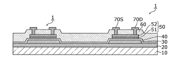
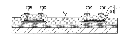
- FIG. 1 is a cross-sectional view illustrating a configuration of a thin film transistor according to an embodiment.
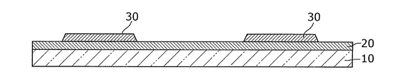
- FIG. 2A is a cross-sectional view of a substrate preparation step in the method of manufacturing a thin film transistor according to the embodiment.
- FIG. 2B is a cross-sectional view of the undercoat forming step in the method for manufacturing the thin film transistor according to the embodiment.
- FIG. 2C is a cross-sectional view of the gate electrode formation step in the method for manufacturing the thin film transistor according to the embodiment.
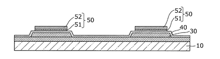
- FIG. 2D is a cross-sectional view of the gate insulating layer forming step in the method for manufacturing the thin film transistor according to the embodiment.
- FIG. 1 is a cross-sectional view illustrating a configuration of a thin film transistor according to an embodiment.
- FIG. 2A is a cross-sectional view of a substrate preparation step in the method of manufacturing a thin film transistor according to the embodiment.
- FIG. 2B is a cross-sectional view of the undercoat forming step
- FIG. 2E is a cross-sectional view of the oxide semiconductor layer forming step in the method for manufacturing the thin film transistor according to the embodiment.
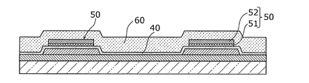
- FIG. 2F is a cross-sectional view of a protective layer forming step in the method for manufacturing the thin film transistor according to the embodiment.
- FIG. 2G is a cross-sectional view of a source electrode and drain electrode formation step in the method of manufacturing a thin film transistor according to the embodiment.
- FIG. 3 is a diagram illustrating measurement results of sheet resistance values when the oxide semiconductor layer contains fluorine and when no fluorine is contained.
- FIG. 4 is a cross-sectional view of a device structure of a sample used in an experiment regarding hydrogen resistance.
- FIG. 5 is a diagram showing the ⁇ -PCD peak intensity and the resistance value of the oxide semiconductor layer when the thickness of the silicon oxide layer is changed for the sample having the structure shown in FIG.
- FIG. 6 is a diagram showing a result of comparing the peak intensity of ⁇ -PCD and the presence or absence of fluorine introduction into the oxide semiconductor layer.
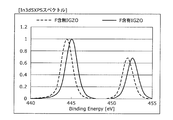
- FIG. 7A is a graph showing XPS spectra of In3d5 when fluorine is contained in an oxide semiconductor layer and when fluorine is not contained in the oxide semiconductor layer.
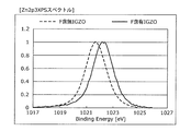
- FIG. 7B is a diagram illustrating an XPS spectrum of Zn2p3 when the oxide semiconductor layer contains fluorine and when no fluorine is contained.
- FIG. 7C is a diagram illustrating an XPS spectrum of Ga2p3 when the oxide semiconductor layer contains fluorine and when no fluorine is contained.
- FIG. 8 is a diagram illustrating temperature-programmed desorption spectra of Zn by a TDS method when fluorine is contained in an oxide semiconductor and when fluorine is not contained.
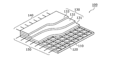
- FIG. 9 is a partially cutaway perspective view of the organic EL display device according to the embodiment.
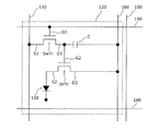
- FIG. 10 is an electric circuit diagram of a pixel circuit in the organic EL display device shown in FIG.
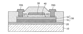
- FIG. 11 is a cross-sectional view illustrating a configuration of a thin film transistor according to a modification.
- a thin film transistor includes a gate electrode, a source electrode and a drain electrode, an oxide semiconductor layer used as a channel layer, and a gate insulating layer disposed between the gate electrode and the oxide semiconductor layer.
- a metal element constituting the oxide semiconductor layer includes at least indium, and an inner region of the oxide semiconductor layer and a region adjacent to the gate insulating layer includes fluorine. It is a thing.
- fluorine is contained in the inner region of the oxide semiconductor layer and in the region adjacent to the gate insulating layer.
- Fluorine has a higher binding energy with metals than oxygen. Therefore, by including fluorine in the oxide semiconductor layer, dangling bonds or unstable sites due to oxygen vacancies in the oxide semiconductor layer can be easily terminated with fluorine. In other words, by containing fluorine in the oxide semiconductor layer, oxygen vacancies in the oxide semiconductor layer can be supplemented.
- the oxide semiconductor layer when fluorine is contained in the oxide semiconductor layer, hydrogen mixed in the oxide semiconductor layer cannot be bonded to the oxide semiconductor layer. Accordingly, entry of hydrogen into the oxide semiconductor layer can be blocked, so that oxygen and hydrogen can be prevented from being combined and released from carriers in the oxide semiconductor layer. That is, the hydrogen resistance of the oxide semiconductor layer can be improved by containing fluorine in the oxide semiconductor layer.
- the oxide semiconductor layer contains fluorine
- a metal element included in the oxide semiconductor layer is chemically bonded to fluorine, so that the structure of the oxide semiconductor layer can be stabilized.
- the film thickness of the region containing fluorine in the oxide semiconductor layer is preferably at least 5 nm.
- the above fluorine-containing effect can be sufficiently exhibited.
- the film thickness of the region containing fluorine in the oxide semiconductor layer is preferably at least 20 nm.
- annealing treatment is performed for the purpose of stabilizing the characteristics of the oxide semiconductor layer.
- hydrogen may diffuse into the oxide semiconductor layer due to the annealing treatment. Therefore, by setting the film thickness of the fluorine-containing region in the oxide semiconductor layer to 20 nm or more, even if hydrogen is diffused by an annealing process or the like, the oxide semiconductor layer is formed in the oxide semiconductor layer by the fluorine-containing region of the oxide semiconductor layer. It can block the mixing of hydrogen.
- the fluorine-containing concentration of the oxide semiconductor layer may be higher than at least the hydrogen-containing concentration of the oxide semiconductor layer.
- the above fluorine-containing effect can be effectively exhibited.
- the metal element included in the oxide semiconductor layer may further include at least one or both of gallium and zinc.
- the gate electrode, the gate insulating layer, and the oxide semiconductor layer are stacked over the substrate in this order, and the source electrode and the drain electrode are It may be formed above the physical semiconductor layer.
- the thin film transistor according to one embodiment of the present invention may further include a channel protective layer formed over the oxide semiconductor layer.
- process damage on the back channel side of the oxide semiconductor layer (channel layer) can be reduced.
- the oxide semiconductor layer, the gate insulating layer, and the gate electrode are stacked over the substrate in this order, and the source electrode is formed over the gate insulating layer.
- the drain electrode is connected to the drain region of the oxide semiconductor layer through a contact hole formed in the gate insulating layer. It is good to have.
- a method for manufacturing a thin film transistor includes a step of forming a gate electrode, a step of forming a source electrode and a drain electrode, a step of forming an oxide semiconductor layer used as a channel layer, Forming a gate insulating layer so as to be positioned between the gate electrode and the oxide semiconductor layer, wherein the metal element constituting the oxide semiconductor layer contains at least indium, and the oxide
- the oxide semiconductor layer is formed while introducing fluorine.
- a thin film transistor having an oxide semiconductor layer that is not easily damaged by hydrogen or oxygen and has a stable structure can be obtained. Therefore, a thin film transistor having high reliability and high robustness can be obtained.
- the fluorine is contained in an inner region of the oxide semiconductor layer and in a region adjacent to the gate insulating layer.
- the oxide semiconductor layer is preferably formed.
- the oxide semiconductor layer in the step of forming the oxide semiconductor layer, may be formed by sputtering using a target material containing fluorine.
- the oxide semiconductor layer containing fluorine can be formed by sputtering.
- the oxide semiconductor layer in the step of forming the oxide semiconductor layer, may be formed using a gas containing fluorine.
- an oxide semiconductor layer containing fluorine can be formed by supplying a gas containing fluorine.
- the film thickness of the region containing fluorine in the oxide semiconductor layer is preferably at least 5 nm.
- a thin film transistor that can sufficiently exhibit the above-described fluorine-containing effect can be obtained.
- the film thickness of the region containing fluorine in the oxide semiconductor layer is preferably at least 20 nm.
- the process control of the oxide semiconductor layer can be sufficiently performed by setting the fluorine-containing region to 20 nm or more.
- the fluorine-containing concentration of the oxide semiconductor layer may be higher than at least the hydrogen-containing concentration of the oxide semiconductor layer.
- the metal element included in the oxide semiconductor layer may further include at least one or both of gallium and zinc.
- the step of forming the gate electrode, the step of forming the gate insulating layer, the step of forming the oxide semiconductor layer, the source electrode, and the The step of forming the drain electrode may be performed in this order.
- the method for manufacturing a thin film transistor according to one embodiment of the present invention may further include a step of forming a channel protective layer over the oxide semiconductor layer.
- a bottom-gate thin film transistor capable of reducing process damage on the back channel side of the oxide semiconductor layer can be obtained.
- the step of forming the oxide semiconductor layer, the step of forming the gate insulating layer, the step of forming the gate electrode, the source electrode, and the The step of forming the drain electrode may be performed in this order.
- a thin film transistor capable of reducing parasitic capacitance can be obtained.
- An organic EL display device is an organic EL display device including any of the thin film transistors described above, and includes a plurality of pixels arranged in a matrix and each of the plurality of pixels.
- the thin film transistor is a driving transistor for driving the organic EL element.
- the thin film transistor having high reliability and high robustness is used as the driving transistor for driving the organic EL element, an organic EL display device excellent in display performance can be realized.
- FIG. 1 is a cross-sectional view showing a configuration of a thin film transistor according to an embodiment of the present invention.
- FIG. 1 two thin film transistors 1 are shown, and the two thin film transistors 1 have the same structure.
- a thin film transistor 1 is a bottom-gate oxide semiconductor TFT having an oxide semiconductor layer as a channel layer.
- the thin film transistor 1 includes a substrate 10, an undercoat layer 20, a gate electrode 30, a gate insulating layer 40, an oxide semiconductor layer 50, a protective layer 60, a source electrode 70S, and a drain electrode 70D.
- the substrate 10 is a glass substrate made of a glass material such as quartz glass, non-alkali glass, or high heat resistant glass.
- the substrate 10 is not limited to a glass substrate but may be a resin substrate or the like.
- substrate 10 may be a flexible substrate comprised not with a rigid board
- the undercoat layer 20 is formed on the substrate 10.
- impurities such as sodium and phosphorus contained in the substrate 10 (glass substrate), moisture transmitted from the atmosphere, and the like are transmitted to the gate electrode 30, the gate insulating layer 40, and the oxide semiconductor layer. 50 can be prevented from entering.
- the undercoat layer 20 is a single-layer insulating layer or a laminated insulating layer using an oxide insulating layer or a nitride insulating layer.
- the undercoat layer 20 may be a single layer film such as silicon nitride (SiN x ), silicon oxide (SiO y ), silicon oxynitride (SiO y N x ), or aluminum oxide (AlO x ), or these A laminated film can be used.
- the film thickness of the undercoat layer 20 is preferably set to 100 nm to 500 nm. Note that the undercoat layer 20 is not necessarily formed.
- the gate electrode 30 is located above the substrate 10 and is patterned in a predetermined shape on the undercoat layer 20.
- the gate electrode 30 is an electrode having a single layer structure or a multilayer structure such as a conductive material such as a metal or an alloy thereof, for example, molybdenum (Mo), aluminum (Al), copper (Cu), tungsten (W), titanium. (Ti), chromium (Cr), molybdenum tungsten (MoW), or the like.
- the film thickness of the gate electrode 30 is preferably set to 50 nm to 300 nm.
- the gate insulating layer 40 is formed so as to be located above the gate electrode 30.
- the gate insulating layer 40 is formed on the undercoat layer 20 so as to cover the gate electrode 30.
- the gate insulating layer 40 is disposed between the gate electrode 30 and the oxide semiconductor layer 50.
- the gate insulating layer 40 is a single-layer insulating layer or a stacked insulating layer using an oxide insulating layer or a nitride insulating layer.
- a single layer film such as silicon oxide, silicon nitride, silicon oxynitride, tantalum oxide, or aluminum oxide, or a laminated film of these can be used.
- the gate insulating layer 40 is, for example, a stacked film of a silicon oxide film and a silicon nitride film.
- the film thickness of the gate insulating layer 40 can be designed in consideration of the breakdown voltage of the TFT, and is preferably 50 nm to 500 nm, for example.
- the oxide semiconductor layer 50 is used as a channel layer. That is, the oxide semiconductor layer 50 is a semiconductor layer including a channel region facing the gate electrode 30 with the gate insulating layer 40 interposed therebetween. The oxide semiconductor layer 50 is formed in a predetermined shape on the gate insulating layer 40.
- the oxide semiconductor layer 50 for example, a transparent amorphous oxide semiconductor (TAOS: Transparent Amorphous Oxide Semiconductor) is used.
- TAOS Transparent Amorphous Oxide Semiconductor
- the metal element included in the oxide semiconductor layer 50 includes at least indium (In), and may further include at least one or both of gallium (Ga) and zinc (Zn).
- the oxide semiconductor layer 50 in this embodiment includes InGaZnO x (IGZO), which is an oxide containing indium (In), gallium (Ga), and zinc (Zn).
- IGZO InGaZnO x
- the oxide semiconductor layer 50 contains fluorine (F). Specifically, fluorine is contained in an inner region of the oxide semiconductor layer 50 and in a region adjacent to the gate insulating layer 40. That is, fluorine is contained on the front channel side of the oxide semiconductor layer 50. In the oxide semiconductor layer 50, fluorine is mixed in a chemically bonded state. Note that the region inside the oxide semiconductor layer 50 that is close to the gate insulating layer 40 is a region closer to the gate insulating layer 40 than at least half the thickness of the oxide semiconductor layer 50.
- the oxide semiconductor layer 50 in this embodiment includes a first region (fluorine-containing region) 51 that is a region containing fluorine and a second region (fluorine-free region) that is a region not containing fluorine. 52.
- the first region 51 is a region on the gate insulating layer 40 side in the oxide semiconductor layer 50. That is, in this embodiment, fluorine is contained only in the region of the oxide semiconductor layer 50 on the gate insulating layer 40 side.
- the first region 51 is a region (lower layer) below the center of the thickness of the oxide semiconductor layer 50 when the center of the thickness of the oxide semiconductor layer 50 is used as a reference, and the second region 52 is oxidized. This is an upper region (upper layer) from the film thickness center of the physical semiconductor layer 50.
- fluorine is included in a part of the oxide semiconductor layer 50; however, fluorine may be included in the entire region of the oxide semiconductor layer 50. That is, the second region 52 may not be provided.
- the film thickness of the first region 51 is at least 5 nm or more, and is 20 nm or more in the present embodiment.
- the film thickness of the oxide semiconductor layer 50 is preferably 20 nm or more.
- the film thickness of the first region 51 is 5 nm or more, the above-described fluorine-containing effect can be sufficiently exhibited.
- the film thickness of the first region 51 is set to 20 nm or more, even when hydrogen diffuses into the oxide semiconductor layer 50 by annealing or the like, the hydrogen diffused by the first region 51 containing fluorine. Can be blocked.
- the first region 51 is close to the gate insulating layer 40, hydrogen that enters the oxide semiconductor layer 50 from the gate insulating layer 40 side is separated from the gate insulating layer 40 in the oxide semiconductor layer 50. It is possible to block in the adjacent area (first area 51).
- the process control of the oxide semiconductor layer 50 can be sufficiently performed. That is, by setting the thickness of the first region 51 to at least 20 nm or more, the thickness of the oxide semiconductor layer 50 can be set to at least 20 nm or more. Accordingly, film formation by sputtering or the like of the oxide semiconductor layer 50 and patterning by photolithography, etching, or the like can be easily performed.
- the fluorine-containing concentration of the oxide semiconductor layer 50 is higher than at least the hydrogen-containing concentration of the oxide semiconductor layer 50.
- the oxide semiconductor layer 50 has a fluorine-containing concentration of 1 ⁇ 10 22 atm / cm 3 or more.
- the protective layer 60 is formed on the oxide semiconductor layer 50.
- the protective layer 60 is a channel region protective layer that protects the channel region of the oxide semiconductor layer 50, and functions as an etching stopper layer. Accordingly, process damage on the back channel side of the oxide semiconductor layer 50 can be reduced in the bottom-gate TFT.
- the protective layer 60 is an interlayer insulating layer formed on the entire surface of the substrate 10.
- the protective layer 60 may be formed of a material mainly composed of an organic substance, or may be formed of an inorganic substance such as silicon oxide, silicon nitride, silicon oxynitride, or aluminum oxide. In the present embodiment, the protective layer 60 is made of a material whose main component is an organic substance. The protective layer 60 may be a single layer film or a laminated film.
- the silicon oxide film has a lower hydrogen content than the silicon nitride film. Therefore, by using a silicon oxide film as the protective layer 60, performance deterioration of the oxide semiconductor layer 50 due to hydrogen can be suppressed. Furthermore, by using an aluminum oxide film as the protective layer 60, hydrogen and oxygen generated in the upper layer can be blocked by the aluminum oxide film. For these reasons, as the protective layer 60, for example, a laminated film having a three-layer structure of a silicon oxide film, an aluminum oxide film, and a silicon oxide film may be used.
- an opening is formed in the protective layer 60 so as to penetrate a part of the protective layer 60.
- the oxide semiconductor layer 50 is connected to the source electrode 70S and the drain electrode 70D through the opening of the protective layer 60.
- the source electrode 70S and the drain electrode 70D are formed on the protective layer 60 in a predetermined shape.
- the source electrode 70 ⁇ / b> S is connected to the oxide semiconductor layer 50 through an opening formed in the protective layer 60
- the drain electrode 70 ⁇ / b> D is connected to the oxide semiconductor layer 50 through an opening formed in the protective layer 60. It is connected to the.
- the source electrode 70S and the drain electrode 70D are electrodes having a single layer structure or a multilayer structure such as a conductive material or an alloy thereof.
- Examples of the material of the source electrode 70S and the drain electrode 70D include molybdenum (Mo), aluminum (Al), copper (Cu), tungsten (W), titanium (Ti), chromium (Cr), and molybdenum tungsten alloy (MoW).
- Mo molybdenum
- Al aluminum
- Cu copper
- W tungsten
- Ti titanium
- Cr chromium
- MoW molybdenum tungsten alloy
- CuMn copper manganese alloy
- the film thickness of the source electrode 70S and the drain electrode 70D is preferably set to, for example, 50 nm to 300 nm.
- FIGS. 2A to 2G are cross-sectional views of each step in the method of manufacturing the thin film transistor according to the embodiment of the present invention.
- a substrate 10 is prepared.
- a glass substrate is prepared as the substrate 10.
- an undercoat layer 20 is formed on the substrate 10.
- An undercoat layer 20 composed of a silicon nitride film, a silicon oxide film, a silicon oxynitride film, an aluminum oxide film, or the like is formed on the substrate 10 by plasma CVD (Chemical Vapor Deposition) or the like.
- the gate electrode 30 is formed above the substrate 10.
- a metal film made of molybdenum tungsten (MoW) is formed on the undercoat layer 20 by sputtering
- the metal film is patterned using a photolithography method and a wet etching method.
- MoW wet etching can be performed using, for example, a chemical solution in which phosphoric acid (HPO 4 ), nitric acid (HNO 3 ), acetic acid (CH 3 COOH), and water are mixed in a predetermined composition.
- the gate insulating layer 40 is formed above the gate electrode 30.
- the gate insulating layer 40 is formed so as to be positioned between the gate electrode 30 and the oxide semiconductor layer 50.
- the gate insulating layer 40 is formed on the entire upper surface of the substrate 10 by plasma CVD or the like so as to cover the gate electrode 30.
- the gate insulating layer 40 is, for example, a silicon nitride film, a silicon oxide film, a silicon oxynitride film, a tantalum oxide film, an aluminum oxide film, or a laminated film thereof.
- silane gas (SiH 4 ) silane gas
- NH 3 ammonia gas
- N 2 nitrogen gas
- an oxide semiconductor layer 50 having a predetermined shape is formed above the gate insulating layer 40 so as to face at least the gate electrode 30.
- an island-shaped oxidation region including a first region (fluorine-containing region) 51 and a second region (fluorine-free region) 52 is formed.
- a physical semiconductor layer 50 is formed on the gate insulating layer 40.
- the oxide semiconductor layer 50 As a material of the oxide semiconductor layer 50, a transparent amorphous oxide semiconductor of InGaZnO x is used.
- the oxide semiconductor layer 50 made of InGaZnO x can be formed by a vapor deposition method such as a sputtering method or a laser deposition method.
- argon (Ar) gas flows as an inert gas into the vacuum chamber.
- a gas containing oxygen (O 2 ) is introduced as a reactive gas, and a voltage having a predetermined power density is applied to the target material.
- the first oxide semiconductor layer containing fluorine (In—Ga—Zn—O: F) can be formed.
- Introduction (supply) of fluorine into the oxide semiconductor layer can be performed by including fluorine in the target or introducing a process gas (such as NF 3 gas) containing fluorine.
- the first oxide semiconductor layer containing fluorine can be formed by forming an InGaZnO x film by sputtering using a target material containing fluorine.
- the first oxide semiconductor layer containing fluorine can be formed by forming the InGaZnO x film using a gas containing fluorine (NF 3 gas or the like).
- a second oxide semiconductor layer (In—Ga—Zn—O) containing no fluorine is formed by performing sputtering or the like without introducing (supplying) fluorine. Note that in this embodiment, the first oxide semiconductor layer and the second oxide semiconductor layer are continuously formed in the same chamber.
- an oxide semiconductor film having a stacked structure of the first oxide semiconductor layer and the second oxide semiconductor layer is patterned by using a photolithography method and a wet etching method, whereby the oxide semiconductor layer 50 having a predetermined shape is formed. Can be formed.
- a resist having a predetermined shape is formed over the oxide semiconductor film, and the oxide semiconductor film in a region where the resist is not formed is removed by wet etching, whereby the island-shaped oxide semiconductor layer 50 is formed.
- the oxide semiconductor film is InGaZnO x
- a chemical solution in which phosphoric acid (H 3 PO 4 ), nitric acid (HNO 3 ), acetic acid (CH 3 COOH), and water are mixed can be used as the etching solution. Good.
- a protective layer 60 is formed on the gate insulating layer 40 so as to cover the oxide semiconductor layer 50.
- the protective layer 60 may be an organic material as a main component or an inorganic material such as a silicon oxide film.
- an opening is formed in the protective layer 60 so that a part of the oxide semiconductor layer 50 is exposed.
- a part of the protective layer 60 is removed by etching by a photolithography method and an etching method, so that an opening is formed on a connection portion between the source electrode 70S and the drain electrode 70D in the oxide semiconductor layer 50.
- the opening can be formed in the silicon oxide film by a dry etching method using a reactive ion etching (RIE) method.
- RIE reactive ion etching
- carbon tetrafluoride (CF 4 ) and oxygen gas (O 2 ) can be used as the etching gas.
- a source electrode 70S and a drain electrode 70D connected to the oxide semiconductor layer 50 through an opening formed in the protective layer 60 are formed.
- a metal film source / drain metal film
- a photolithography method and a wet etching method are used.
- a source electrode 70S and a drain electrode 70D having a predetermined shape are formed.
- heat treatment annealing
- oxygen vacancies in the oxide semiconductor layer 50 can be repaired, and the characteristics of the oxide semiconductor layer 50 can be stabilized.
- the electrical characteristics of an oxide semiconductor TFT having an oxide semiconductor layer are easily affected by oxygen and hydrogen. For this reason, the oxide semiconductor TFT has problems in stability and reliability.
- Patent Document 2 As disclosed in Patent Document 2 and Non-Patent Document 2, there have been reports that stability and reliability can be improved by improving the interface between the insulating layer and the oxide semiconductor layer.
- Non-Patent Document 2 fluorine is added to the dangling bond site of In that forms an oxide semiconductor layer by improving the interface with the oxide semiconductor layer (IGZO) using a gate insulating layer mixed with fluorine. It has been reported that complementation is generated, which leads to improved reliability.
- Non-Patent Document 2 the oxide semiconductor layer (IGZO) was measured by secondary ion mass spectrometry (SIMS), and as a result, fluorine contamination could not be observed in the bulk of IGZO. It has also been reported.
- SIMS secondary ion mass spectrometry
- a gate insulating layer mixed with fluorine includes an insulating layer, an oxide semiconductor layer, and the like. It is thought that the improvement effect at the interface of the entire time.
- the oxide semiconductor TFT not only the interface between the insulating layer and the oxide semiconductor layer but also the process damage caused by hydrogen or the like in the manufacturing process causes variations in characteristics and a decrease in reliability. Therefore, it is not sufficient to improve only the interface between the insulating layer and the oxide semiconductor layer.
- the present invention has been made on the basis of such knowledge, and the inventor of the present application has an idea that a highly reliable thin film transistor can be obtained by containing fluorine in the oxide semiconductor layer 50 as described above. Got.
- the inventors of the present application conducted various experiments in order to verify that a highly reliable thin film transistor can be obtained by containing fluorine in the oxide semiconductor layer.
- the experiment and the analysis will be described.
- an InGaZnO x film in which the main component of the metal element is In, Ga, or Zn was used as the oxide semiconductor layer 50.
- FIG. 3 shows the result of measuring the sheet resistance value in vacuum heating (300 ° C.) when the oxide semiconductor layer contains fluorine and when no fluorine is contained using a four-terminal measurement method. Is shown.
- the sheet resistance value in the case where fluorine is not contained in the oxide semiconductor layer 50 is as low as about 1 ⁇ 10 5 ⁇ / ⁇ .
- the sheet resistance value when fluorine is contained in the oxide semiconductor layer 50 is the measurement limit (> 1 ⁇ 10 10 ⁇ / ⁇ ), which is a resistance value as compared with the case where fluorine is not contained. Is rising.
- fluorine has higher bond energy with metal than oxygen, so that the oxide semiconductor layer 50 can contain dangling bonds or unstable sites due to oxygen vacancies in the oxide semiconductor layer 50 by fluorine. It is because it can be terminated with.
- FIG. 4 is a cross-sectional view showing the device structure of the sample used in this experiment.
- IGZO oxide semiconductor layer
- SiO silicon oxide layer
- SiN silicon nitride layer containing hydrogen
- FIG. 5 is a diagram showing the ⁇ -PCD peak intensity and the resistance value of the oxide semiconductor layer when the thickness of the silicon oxide layer is changed for the sample having the structure shown in FIG.
- the film thickness of the silicon oxide layer is changed to 10 nm, 120 nm, and 240 nm.
- the resistance value of the oxide semiconductor layer was measured by a non-contact resistance measuring device.
- the resistance value of the oxide semiconductor layer (IGZO) and the peak intensity of ⁇ -PCD have a positive correlation. That is, it can be seen that the resistance value of the oxide semiconductor layer (IGZO) and the peak intensity of ⁇ -PCD are one guideline for determining hydrogen-induced damage due to the presence or absence of fluorine introduction.
- FIG. 6 shows the result of comparison between the peak intensity of ⁇ -PCD and the presence or absence of fluorine introduction into the oxide semiconductor layer.
- the ⁇ -PCD intensity value in the oxide semiconductor layer (peak intensity value before SiN: H film formation and peak intensity after SiN: H film formation). It can be seen that the ratio to the value decreases. That is, it can be seen that when the resistance value is low, the resistance value hardly changes even when fluorine is introduced, that is, the resistance value does not decrease.
- the mixed hydrogen is combined with oxygen in the oxide semiconductor layer and carriers are released.
- FIGS. 7A to 7C show XPS of In3d5, Zn1p3, and Ga2p3 when fluorine is contained in the oxide semiconductor layer (IGZO) (F-containing IGZO) and when fluorine is not contained (F-containing IGZO), respectively.
- the spectrum is shown.
- the peak position of the XPS spectrum of In3d5 is shifted to the higher binding energy side by 0.5 eV or more. That is, the In3d5 peak position measured by XPS in the F-containing IGZO is shifted to a higher energy side by at least 0.5 eV or more compared to the In3d5 peak position in the F-free IGZO.
- the inclusion of fluorine shifts the peak position of the XPS spectrum of Zn2p3 to 0.4 eV or higher binding energy side. That is, the Zn2p3 peak position measured by XPS in the F-containing IGZO is shifted to a higher energy side by at least 0.4 eV or more compared to the peak position of Zn2p3 in the F-free IGZO.
- the peak position of the XPS spectrum of Ga2p3 is shifted to the high binding energy side by 0.5 eV or more by containing fluorine. That is, the Ga2p3 peak position measured by XPS in the F-containing IGZO is shifted to a higher energy side by at least 0.5 eV or more compared to the Ga2p3 peak position in the F-free IGZO.
- the fluorine is not simply mixed into the oxide semiconductor layer 50, but constitutes the oxide semiconductor layer. It can be seen that they are mixed in a state of being chemically bonded to the elements to be treated. As a result, the metal element constituting the oxide semiconductor layer 50 is difficult to escape.
- the oxide semiconductor layer 50 contains fluorine
- the metal element included in the oxide semiconductor layer 50 is chemically bonded to fluorine, so that the structure of the oxide semiconductor layer 50 is changed in a stable direction. Can do. Thereby, a highly reliable thin film transistor can be obtained.
- FIG. 8 shows Zn by TDS (Thermal Desorption Spectrometry) method in the case where fluorine is contained in the oxide semiconductor layer 50 (IGZO) (F-containing IGZO) and in the case where fluorine is not contained (F-containing IGZO). Shows the temperature-programmed desorption spectrum.
- the fluorine-containing concentration of the oxide semiconductor layer 50 when fluorine was contained was 1 ⁇ 10 22 atm / cm 3 or more.
- the horizontal axis indicates the temperature (° C.) at which Zn is temperature-desorbed and the vertical axis indicates the amount of Zn that is temperature-desorbed (arbitrary unit).
- the temperature-programmed desorption of Zn in the oxide semiconductor layer 50 (F-containing IGZO) in the case of containing fluorine is the oxide semiconductor layer 50 (F-free IGZO) in the case of not containing fluorine. It can be seen that desorption from a high temperature of 50 ° C. or more is achieved as compared with the temperature-programmed desorption of Zn. That is, when the oxide semiconductor layer 50 contains fluorine so that the fluorine-containing concentration is at least 1 ⁇ 10 22 atm / cm 3 or more, the temperature at which Zn is desorbed by heating (temperature-desorbing desorption temperature) is 50. It can be seen that the temperature rises.
- the temperature-programmed desorption temperature can be used as a physical property index of the oxide semiconductor layer, and an increase in the temperature-programmed desorption temperature indicates that the structure is stabilized.
- the oxide semiconductor layer 50 contains fluorine
- the metal element constituting the oxide semiconductor layer 50 is chemically bonded to fluorine, so that the oxide semiconductor The structure of the layer 50 can be stabilized.
- the oxide semiconductor layer 50 contains fluorine.
- fluorine is contained in an inner region of the oxide semiconductor layer 50 and in a region adjacent to the gate insulating layer 40.
- oxygen vacancies in the oxide semiconductor layer 50 can be complemented, the hydrogen resistance of the oxide semiconductor layer 50 can be improved, and the structure of the oxide semiconductor layer 50 can be improved. Can be stabilized. Therefore, the thin film transistor 1 having high reliability and high robustness can be realized.
- FIG. 9 is a partially cutaway perspective view of the organic EL display device according to the embodiment of the present invention.
- FIG. 10 is an electric circuit diagram of a pixel circuit in the organic EL display device shown in FIG. Note that the pixel circuit is not limited to the configuration shown in FIG.
- the above-described thin film transistor 1 can be used as a switching transistor SwTr and a drive transistor DrTr of an active matrix substrate in an organic EL display device.
- the organic EL display device 100 includes a TFT substrate (TFT array substrate) 110 on which a plurality of thin film transistors are arranged, an anode 131 as a lower electrode (reflection electrode), and an EL layer (light emitting layer) 132. And a laminated structure with an organic EL element (light emitting part) 130 composed of a cathode 133 which is an upper electrode (transparent electrode).
- the thin film transistor 1 described above is used for the TFT substrate 110 in the present embodiment.
- a plurality of pixels 120 are arranged in a matrix on the TFT substrate 110, and each pixel 120 is provided with a pixel circuit.
- the organic EL element 130 is formed corresponding to each of the plurality of pixels 120, and the light emission of each organic EL element 130 is controlled by a pixel circuit provided in each pixel 120.
- the organic EL element 130 is formed on an interlayer insulating layer (planarization film) formed so as to cover a plurality of thin film transistors.
- the organic EL element 130 has a configuration in which an EL layer 132 is disposed between the anode 131 and the cathode 133.
- a hole transport layer is further laminated between the anode 131 and the EL layer 132, and an electron transport layer is further laminated between the EL layer 132 and the cathode 133.
- another functional layer may be provided between the anode 131 and the cathode 133.
- the functional layer formed between the anode 131 and the cathode 133 including the EL layer 132 is an organic layer made of an organic material.
- Each pixel 120 is driven and controlled by each pixel circuit.
- the TFT substrate 110 includes a plurality of gate wirings (scanning lines) 140 arranged along the row direction of the pixels 120 and a plurality of gate wirings 140 arranged along the column direction of the pixels 120 so as to intersect the gate wiring 140.
- Source wiring (signal wiring) 150 and a plurality of power supply wirings (not shown in FIG. 9) arranged in parallel with the source wiring 150 are formed.
- Each pixel 120 is partitioned by, for example, an orthogonal gate wiring 140 and a source wiring 150.
- the gate wiring 140 is connected to the gate electrode of the switching transistor included in each pixel circuit for each row.
- the source wiring 150 is connected to the source electrode of the switching transistor for each column.
- the power supply wiring is connected to the drain electrode of the drive transistor included in each pixel circuit for each column.
- the pixel circuit includes a switching transistor SwTr, a drive transistor DrTr, and a capacitor C that stores data to be displayed on the corresponding pixel 120.
- the switching transistor SwTr is a TFT for selecting the pixel 120
- the drive transistor DrTr is a TFT for driving the organic EL element 130.
- the switching transistor SwTr includes a gate electrode G1 connected to the gate wiring 140, a source electrode S1 connected to the source wiring 150, a drain electrode D1 connected to the capacitor C and the gate electrode G2 of the second thin film transistor DrTr, and an oxidation A physical semiconductor layer (not shown).
- the switching transistor SwTr when a predetermined voltage is applied to the connected gate wiring 140 and source wiring 150, the voltage applied to the source wiring 150 is stored in the capacitor C as a data voltage.
- the drive transistor DrTr is connected to the drain electrode D1 of the switching transistor SwTr and the gate electrode G2 connected to the capacitor C, the drain electrode D2 connected to the power supply wiring 160 and the capacitor C, and the anode 131 of the organic EL element 130.
- a source electrode S2 and an oxide semiconductor layer are provided.
- the drive transistor DrTr supplies a current corresponding to the data voltage held by the capacitor C from the power supply wiring 160 to the anode 131 of the organic EL element 130 through the source electrode S2. Thereby, in the organic EL element 130, a drive current flows from the anode 131 to the cathode 133, and the EL layer 132 emits light.
- the organic EL display device 100 having the above configuration employs an active matrix system in which display control is performed for each pixel 120 located at the intersection of the gate wiring 140 and the source wiring 150. Thereby, the corresponding organic EL element 130 selectively emits light by the switching transistor SwTr and the drive transistor DrTr in each pixel 120, and a desired image is displayed.
- the thin film transistor 1 having high reliability and high robustness is used as the switching transistor SwTr and the drive transistor DrTr, an organic EL display device excellent in reliability is realized. it can.
- the thin film transistor 1 is used as the drive transistor DrTr for driving the organic EL element 130, an organic EL display device having excellent display performance can be realized.
- an amorphous oxide semiconductor such as InGaZnO x (IGZO) is used as an oxide semiconductor used for the oxide semiconductor layer.
- IGZO amorphous oxide semiconductor
- the present invention is not limited to this, and In oxide such as a polycrystalline oxide semiconductor such as InGaO is used.
- An oxide semiconductor containing can be used.
- a top-gate thin film transistor in which the oxide semiconductor layer 50, the gate insulating layer 40, and the gate electrode 30 are stacked on the substrate 10 in this order from the bottom may be used.
- the source electrode 70S is connected to the source region (low-resistance region) 50S of the oxide semiconductor layer 50 through a contact hole formed in the gate insulating layer 40.
- the drain electrode 70 ⁇ / b> D is connected to the drain region (low resistance region) 50 ⁇ / b> D of the oxide semiconductor layer 50 through a contact hole formed in the gate insulating layer 40.
- the parasitic capacitance can be reduced.
- an organic EL display device has been described as a display device using a thin film transistor, but the present invention is not limited to this.
- the thin film transistor in the above embodiment can also be applied to other display devices such as a liquid crystal display device.
- the organic EL display device (organic EL panel) can be used as a flat panel display.
- the organic EL display device can be used as a display panel of any electronic device such as a television set, a personal computer, or a mobile phone.
- the thin film transistor according to the present invention can be widely used in various electric devices having a thin film transistor such as a display device (display panel) such as an organic EL display device, a television set, a personal computer, and a mobile phone using the display device. it can.
- a display device display panel
- organic EL display device such as an organic EL display device
- a television set such as a television set, a personal computer, and a mobile phone using the display device. it can.
Landscapes
- Thin Film Transistor (AREA)
- Devices For Indicating Variable Information By Combining Individual Elements (AREA)
- Electroluminescent Light Sources (AREA)
- Physical Deposition Of Substances That Are Components Of Semiconductor Devices (AREA)
Abstract
Description
以下、本発明の一実施の形態について、図面を用いて説明する。なお、以下に説明する実施の形態は、いずれも本発明の好ましい一具体例を示すものである。したがって、以下の実施の形態で示される、数値、形状、材料、構成要素、構成要素の配置位置及び接続形態、工程(ステップ)、工程の順序等は、一例であって本発明を限定する主旨ではない。よって、以下の実施の形態における構成要素のうち、本発明の最上位概念を示す独立請求項に記載されていない構成要素については、任意の構成要素として説明される。
まず、本発明の実施の形態に係る薄膜トランジスタ1について、図1を用いて説明する。図1は、本発明の実施の形態に係る薄膜トランジスタの構成を示す断面図である。なお、図1には2つの薄膜トランジスタ1が図示されており、2つの薄膜トランジスタ1は同じ構造である。
次に、本実施の形態に係る薄膜トランジスタ1の製造方法について、図2A~図2Gを用いて説明する。図2A~図2Gは、本発明の実施の形態に係る薄膜トランジスタの製造方法における各工程の断面図である。
次に、本実施の形態に係る薄膜トランジスタ1の作用効果について、本発明に至った経緯も含めて説明する。
次に、上記の実施の形態に係る薄膜トランジスタ1を表示装置に適用した例について、図9及び図10を用いて説明する。なお、本実施の形態では、有機EL表示装置への適用例について説明する。
以上、薄膜トランジスタ及びその製造方法について、実施の形態に基づいて説明したが、本発明は、上記実施の形態に限定されるものではない。
10 基板
20 アンダーコート層
30、G1、G2 ゲート電極
40 ゲート絶縁層
50 酸化物半導体層
51 第1領域
52 第2領域
50S、S1、S2 ソース領域
50D、D1、D2 ドレイン領域
60 保護層
70S ソース電極
70D ドレイン電極
100 有機EL表示装置
110 TFT基板
120 画素
130 有機EL素子
131 陽極
132 EL層
133 陰極
140 ゲート配線
150 ソース配線
160 電源配線
SwTr スイッチングトランジスタ
DrTr 駆動トランジスタ
C キャパシタ
Claims (20)
- ゲート電極と、
ソース電極及びドレイン電極と、
チャネル層として用いられる酸化物半導体層と、
前記ゲート電極と前記酸化物半導体層との間に配置されたゲート絶縁層とを備え、
前記酸化物半導体層を構成する金属元素には少なくともインジウムが含まれており、
前記酸化物半導体層の内部領域であって前記ゲート絶縁層と近接する領域にはフッ素が含有されている
薄膜トランジスタ。 - 前記酸化物半導体層におけるフッ素が含有されている領域の膜厚は、少なくとも5nm以上である
請求項1に記載の薄膜トランジスタ。 - 前記酸化物半導体層におけるフッ素が含有されている領域の膜厚は、少なくとも20nm以上である
請求項1に記載の薄膜トランジスタ。 - 前記酸化物半導体層のフッ素含有濃度は、少なくとも前記酸化物半導体層の水素含有濃度よりも高い
請求項1~3のいずれか1項に記載の薄膜トランジスタ。 - 前記酸化物半導体層を構成する金属元素には、さらに、ガリウム及び亜鉛の少なくとも一方又は両方が含まれている
請求項1~4のいずれか1項に記載の薄膜トランジスタ。 - 前記ゲート電極、前記ゲート絶縁層及び前記酸化物半導体層は、この順で基板上に積層されており、
前記ソース電極及び前記ドレイン電極は、前記酸化物半導体層の上方に形成されている
請求項1~5のいずれか1項に記載の薄膜トランジスタ。 - さらに、前記酸化物半導体層上に形成されたチャネル保護層を備える
請求項6に記載の薄膜トランジスタ。 - 前記酸化物半導体層、前記ゲート絶縁層及び前記ゲート電極は、この順で基板上に積層されており、
前記ソース電極は、前記ゲート絶縁層に形成されたコンタクトホールを介して前記酸化物半導体層のソース領域に接続されており、
前記ドレイン電極は、前記ゲート絶縁層に形成されたコンタクトホールを介して前記酸化物半導体層のドレイン領域に接続されている
請求項1~5のいずれか1項に記載の薄膜トランジスタ。 - ゲート電極を形成する工程と、
ソース電極及びドレイン電極を形成する工程と、
チャネル層として用いられる酸化物半導体層を形成する工程と、
前記ゲート電極と前記酸化物半導体層との間に位置するようにゲート絶縁層を形成する工程とを含み、
前記酸化物半導体層を構成する金属元素には少なくともインジウムが含まれており、
前記酸化物半導体層を形成する工程では、フッ素を導入しながら前記酸化物半導体層を形成する
薄膜トランジスタの製造方法。 - 前記酸化物半導体層を形成する工程では、前記フッ素が前記酸化物半導体層の内部領域であって前記ゲート絶縁層と近接する領域に含有するように、前記酸化物半導体層を形成する
請求項9に記載の薄膜トランジスタの製造方法。 - 前記酸化物半導体層を形成する工程では、フッ素を含むターゲット材を用いたスパッタによって前記酸化物半導体層を形成する
請求項9又は10に記載の薄膜トランジスタの製造方法。 - 前記酸化物半導体層を形成する工程では、フッ素を含むガスを用いて前記酸化物半導体層を形成する
請求項9又は10に記載の薄膜トランジスタの製造方法。 - 前記酸化物半導体層におけるフッ素が含有されている領域の膜厚は、少なくとも5nm以上である
請求項9~12のいずれか1項に記載の薄膜トランジスタの製造方法。 - 前記酸化物半導体層におけるフッ素が含有されている領域の膜厚は、少なくとも20nm以上である
請求項9~12のいずれか1項に記載の薄膜トランジスタの製造方法。 - 前記酸化物半導体層のフッ素含有濃度は、少なくとも前記酸化物半導体層の水素含有濃度よりも高い
請求項10~14のいずれか1項に記載の薄膜トランジスタの製造方法。 - 前記酸化物半導体層を構成する金属元素には、さらに、ガリウム及び亜鉛の少なくとも一方又は両方が含まれている
請求項10~15のいずれか1項に記載の薄膜トランジスタの製造方法。 - 前記ゲート電極を形成する工程と、前記ゲート絶縁層を形成する工程と、前記酸化物半導体層を形成する工程と、前記ソース電極及び前記ドレイン電極を形成する工程とは、この順で行われる
請求項9~16のいずれか1項に記載の薄膜トランジスタの製造方法。 - さらに、前記酸化物半導体層上にチャネル保護層を形成する工程を含む
請求項16に記載の薄膜トランジスタの製造方法。 - 前記酸化物半導体層を形成する工程と、前記ゲート絶縁層を形成する工程と、前記ゲート電極を形成する工程と、前記ソース電極及び前記ドレイン電極を形成する工程とは、この順で行われる
請求項9~16のいずれか1項に記載の薄膜トランジスタの製造方法。 - 請求項1~8のいずれか1項に記載の薄膜トランジスタを備える有機EL表示装置であって、
マトリクス状に配置された複数の画素と、
前記複数の画素の各々に対応して形成された有機EL素子とを備え、
前記薄膜トランジスタは、前記有機EL素子を駆動する駆動トランジスタである
有機EL表示装置。
Priority Applications (2)
| Application Number | Priority Date | Filing Date | Title |
|---|---|---|---|
| US15/320,297 US20170162713A1 (en) | 2014-06-20 | 2015-06-17 | Thin film transistor, method for manufacturing thin film transistor, and organic el display device |
| JP2016529053A JP6331052B2 (ja) | 2014-06-20 | 2015-06-17 | 薄膜トランジスタ、薄膜トランジスタの製造方法及び有機el表示装置 |
Applications Claiming Priority (2)
| Application Number | Priority Date | Filing Date | Title |
|---|---|---|---|
| JP2014127524 | 2014-06-20 | ||
| JP2014-127524 | 2014-06-20 |
Publications (1)
| Publication Number | Publication Date |
|---|---|
| WO2015194175A1 true WO2015194175A1 (ja) | 2015-12-23 |
Family
ID=54935180
Family Applications (1)
| Application Number | Title | Priority Date | Filing Date |
|---|---|---|---|
| PCT/JP2015/003041 Ceased WO2015194175A1 (ja) | 2014-06-20 | 2015-06-17 | 薄膜トランジスタ、薄膜トランジスタの製造方法及び有機el表示装置 |
Country Status (3)
| Country | Link |
|---|---|
| US (1) | US20170162713A1 (ja) |
| JP (1) | JP6331052B2 (ja) |
| WO (1) | WO2015194175A1 (ja) |
Cited By (1)
| Publication number | Priority date | Publication date | Assignee | Title |
|---|---|---|---|---|
| CN114093889A (zh) * | 2021-11-02 | 2022-02-25 | Tcl华星光电技术有限公司 | 阵列基板及制备方法和显示面板 |
Families Citing this family (4)
| Publication number | Priority date | Publication date | Assignee | Title |
|---|---|---|---|---|
| JP2018125340A (ja) * | 2017-01-30 | 2018-08-09 | 株式会社ジャパンディスプレイ | 表示装置 |
| KR102393552B1 (ko) * | 2017-11-09 | 2022-05-02 | 엘지디스플레이 주식회사 | 수소 차단막을 갖는 박막 트랜지스터 및 이를 포함하는 표시장치 |
| KR102798047B1 (ko) | 2020-12-04 | 2025-04-22 | 삼성디스플레이 주식회사 | 표시 장치 및 그 제조 방법 |
| CN113990994B (zh) * | 2021-09-08 | 2023-11-14 | 华灿光电(浙江)有限公司 | 高稳定发光二极管芯片及其制造方法 |
Citations (3)
| Publication number | Priority date | Publication date | Assignee | Title |
|---|---|---|---|---|
| JP2011205078A (ja) * | 2010-03-05 | 2011-10-13 | Semiconductor Energy Lab Co Ltd | 半導体装置の作製方法 |
| JP2011205081A (ja) * | 2010-03-05 | 2011-10-13 | Semiconductor Energy Lab Co Ltd | 半導体装置、及び半導体装置の作製方法 |
| JP2013093572A (ja) * | 2011-10-05 | 2013-05-16 | Semiconductor Energy Lab Co Ltd | 半導体装置及びその作製方法 |
Family Cites Families (5)
| Publication number | Priority date | Publication date | Assignee | Title |
|---|---|---|---|---|
| WO2009129625A1 (en) * | 2008-04-22 | 2009-10-29 | Merck Frosst Canada Ltd. | Novel substituted heteroaromatic compounds as inhibitors of stearoyl-coenzyme a delta-9 desaturase |
| JP2011137737A (ja) * | 2009-12-28 | 2011-07-14 | Fukuda Crystal Laboratory | 無線測定装置、および無線温度測定システム |
| KR101924078B1 (ko) * | 2012-03-30 | 2018-12-03 | 삼성디스플레이 주식회사 | 유기 발광 표시 장치 및 유기 발광 표시 장치의 리페어 방법 |
| US9871097B2 (en) * | 2014-06-20 | 2018-01-16 | Joled Inc. | Thin film transistor, method for manufacturing thin film transistor, and organic EL display device |
| JP6311901B2 (ja) * | 2014-06-26 | 2018-04-18 | 株式会社Joled | 薄膜トランジスタ及び有機el表示装置 |
-
2015
- 2015-06-17 JP JP2016529053A patent/JP6331052B2/ja active Active
- 2015-06-17 WO PCT/JP2015/003041 patent/WO2015194175A1/ja not_active Ceased
- 2015-06-17 US US15/320,297 patent/US20170162713A1/en not_active Abandoned
Patent Citations (3)
| Publication number | Priority date | Publication date | Assignee | Title |
|---|---|---|---|---|
| JP2011205078A (ja) * | 2010-03-05 | 2011-10-13 | Semiconductor Energy Lab Co Ltd | 半導体装置の作製方法 |
| JP2011205081A (ja) * | 2010-03-05 | 2011-10-13 | Semiconductor Energy Lab Co Ltd | 半導体装置、及び半導体装置の作製方法 |
| JP2013093572A (ja) * | 2011-10-05 | 2013-05-16 | Semiconductor Energy Lab Co Ltd | 半導体装置及びその作製方法 |
Cited By (1)
| Publication number | Priority date | Publication date | Assignee | Title |
|---|---|---|---|---|
| CN114093889A (zh) * | 2021-11-02 | 2022-02-25 | Tcl华星光电技术有限公司 | 阵列基板及制备方法和显示面板 |
Also Published As
| Publication number | Publication date |
|---|---|
| JP6331052B2 (ja) | 2018-05-30 |
| JPWO2015194175A1 (ja) | 2017-06-08 |
| US20170162713A1 (en) | 2017-06-08 |
Similar Documents
| Publication | Publication Date | Title |
|---|---|---|
| JP6311901B2 (ja) | 薄膜トランジスタ及び有機el表示装置 | |
| JP6358596B2 (ja) | 薄膜トランジスタ基板の製造方法 | |
| US10096623B2 (en) | Thin film transistor, method for manufacturing the same, and semiconductor device | |
| US10535779B2 (en) | Thin film transistor and method for manufacturing thin film transistor | |
| US10644165B2 (en) | Thin-film transistor, method of fabricating thin-film transistor, and display device | |
| US10276722B2 (en) | Thin film transistor | |
| WO2016056204A1 (ja) | 薄膜トランジスタ基板、薄膜トランジスタ基板の製造方法、及び、表示パネル | |
| JP2012033836A (ja) | トップゲート型薄膜トランジスタ及びこれを備えた表示装置 | |
| US10204973B2 (en) | Display device and thin-film transistors substrate | |
| WO2014171056A1 (ja) | 薄膜半導体装置、有機el表示装置、及びそれらの製造方法 | |
| JPWO2015029286A1 (ja) | 薄膜トランジスタ基板の製造方法及び薄膜トランジスタ基板 | |
| JP6331052B2 (ja) | 薄膜トランジスタ、薄膜トランジスタの製造方法及び有機el表示装置 | |
| US9893193B2 (en) | Thin-film transistor including a gate electrode with a side wall insulating layer and display device | |
| US20150200113A1 (en) | Method of manufacturing thin-film transistor substrate | |
| JP6263721B2 (ja) | 薄膜トランジスタ、薄膜トランジスタの製造方法及び有機el表示装置 | |
| US20160163838A1 (en) | Method of fabricating thin-film semiconductor substrate | |
| JP6500202B2 (ja) | 薄膜トランジスタ及び薄膜トランジスタの製造方法 | |
| WO2016038823A1 (ja) | 薄膜トランジスタ及び薄膜トランジスタの製造方法 | |
| JP6500203B2 (ja) | 薄膜トランジスタ及び薄膜トランジスタの製造方法 | |
| WO2016067585A1 (ja) | 薄膜半導体装置、有機el表示装置及び薄膜半導体装置の製造方法 | |
| JP2016111092A (ja) | 薄膜トランジスタ |
Legal Events
| Date | Code | Title | Description |
|---|---|---|---|
| 121 | Ep: the epo has been informed by wipo that ep was designated in this application |
Ref document number: 15810040 Country of ref document: EP Kind code of ref document: A1 |
|
| WWE | Wipo information: entry into national phase |
Ref document number: 15320297 Country of ref document: US |
|
| ENP | Entry into the national phase |
Ref document number: 2016529053 Country of ref document: JP Kind code of ref document: A |
|
| NENP | Non-entry into the national phase |
Ref country code: DE |
|
| 122 | Ep: pct application non-entry in european phase |
Ref document number: 15810040 Country of ref document: EP Kind code of ref document: A1 |