WO2015194146A1 - Module de cellule solaire - Google Patents
Module de cellule solaire Download PDFInfo
- Publication number
- WO2015194146A1 WO2015194146A1 PCT/JP2015/002955 JP2015002955W WO2015194146A1 WO 2015194146 A1 WO2015194146 A1 WO 2015194146A1 JP 2015002955 W JP2015002955 W JP 2015002955W WO 2015194146 A1 WO2015194146 A1 WO 2015194146A1
- Authority
- WO
- WIPO (PCT)
- Prior art keywords
- solar cell
- back surface
- filling member
- polymer layer
- intermediate member
- Prior art date
Links
- 239000000463 material Substances 0.000 claims abstract description 56
- 229920000098 polyolefin Polymers 0.000 claims abstract description 53
- 239000002861 polymer material Substances 0.000 claims abstract description 33
- XLYOFNOQVPJJNP-UHFFFAOYSA-N water Substances O XLYOFNOQVPJJNP-UHFFFAOYSA-N 0.000 claims abstract description 27
- 238000010521 absorption reaction Methods 0.000 claims abstract description 12
- 229920000642 polymer Polymers 0.000 claims description 73
- 229910052751 metal Inorganic materials 0.000 claims description 54
- 239000002184 metal Substances 0.000 claims description 54
- -1 polyethylene terephthalate Polymers 0.000 claims description 24
- 239000005020 polyethylene terephthalate Substances 0.000 claims description 12
- 229920000139 polyethylene terephthalate Polymers 0.000 claims description 12
- 239000005038 ethylene vinyl acetate Substances 0.000 claims description 4
- DQXBYHZEEUGOBF-UHFFFAOYSA-N but-3-enoic acid;ethene Chemical group C=C.OC(=O)CC=C DQXBYHZEEUGOBF-UHFFFAOYSA-N 0.000 claims description 2
- 229920001200 poly(ethylene-vinyl acetate) Polymers 0.000 claims description 2
- 230000001681 protective effect Effects 0.000 abstract description 5
- 230000004048 modification Effects 0.000 description 22
- 238000012986 modification Methods 0.000 description 22
- 239000000945 filler Substances 0.000 description 21
- 229910021417 amorphous silicon Inorganic materials 0.000 description 13
- 239000004698 Polyethylene Substances 0.000 description 11
- 238000006243 chemical reaction Methods 0.000 description 11
- 229920000573 polyethylene Polymers 0.000 description 11
- QTBSBXVTEAMEQO-UHFFFAOYSA-N Acetic acid Chemical compound CC(O)=O QTBSBXVTEAMEQO-UHFFFAOYSA-N 0.000 description 10
- 239000000853 adhesive Substances 0.000 description 10
- 230000001070 adhesive effect Effects 0.000 description 10
- 229920005989 resin Polymers 0.000 description 10
- 239000011347 resin Substances 0.000 description 10
- 238000005260 corrosion Methods 0.000 description 9
- 230000007797 corrosion Effects 0.000 description 9
- 238000009792 diffusion process Methods 0.000 description 9
- 229910021421 monocrystalline silicon Inorganic materials 0.000 description 9
- 230000008961 swelling Effects 0.000 description 7
- 239000002245 particle Substances 0.000 description 6
- 230000008859 change Effects 0.000 description 5
- PXHVJJICTQNCMI-UHFFFAOYSA-N Nickel Chemical compound [Ni] PXHVJJICTQNCMI-UHFFFAOYSA-N 0.000 description 4
- XLOMVQKBTHCTTD-UHFFFAOYSA-N Zinc monoxide Chemical compound [Zn]=O XLOMVQKBTHCTTD-UHFFFAOYSA-N 0.000 description 4
- 230000015572 biosynthetic process Effects 0.000 description 4
- 239000004743 Polypropylene Substances 0.000 description 3
- 239000000470 constituent Substances 0.000 description 3
- 238000009434 installation Methods 0.000 description 3
- 229920001155 polypropylene Polymers 0.000 description 3
- 239000004925 Acrylic resin Substances 0.000 description 2
- 229920000178 Acrylic resin Polymers 0.000 description 2
- BQCADISMDOOEFD-UHFFFAOYSA-N Silver Chemical compound [Ag] BQCADISMDOOEFD-UHFFFAOYSA-N 0.000 description 2
- 230000007062 hydrolysis Effects 0.000 description 2
- 238000006460 hydrolysis reaction Methods 0.000 description 2
- 230000001788 irregular Effects 0.000 description 2
- 238000004519 manufacturing process Methods 0.000 description 2
- 238000000034 method Methods 0.000 description 2
- 229910052759 nickel Inorganic materials 0.000 description 2
- 229910052709 silver Inorganic materials 0.000 description 2
- 239000004332 silver Substances 0.000 description 2
- 229910000679 solder Inorganic materials 0.000 description 2
- 239000000758 substrate Substances 0.000 description 2
- 229920001187 thermosetting polymer Polymers 0.000 description 2
- 239000011787 zinc oxide Substances 0.000 description 2
- RYGMFSIKBFXOCR-UHFFFAOYSA-N Copper Chemical compound [Cu] RYGMFSIKBFXOCR-UHFFFAOYSA-N 0.000 description 1
- 229920000219 Ethylene vinyl alcohol Polymers 0.000 description 1
- 239000004372 Polyvinyl alcohol Substances 0.000 description 1
- 229910006404 SnO 2 Inorganic materials 0.000 description 1
- GWEVSGVZZGPLCZ-UHFFFAOYSA-N Titan oxide Chemical compound O=[Ti]=O GWEVSGVZZGPLCZ-UHFFFAOYSA-N 0.000 description 1
- 239000011230 binding agent Substances 0.000 description 1
- 230000000903 blocking effect Effects 0.000 description 1
- 239000000969 carrier Substances 0.000 description 1
- 239000003795 chemical substances by application Substances 0.000 description 1
- 239000011248 coating agent Substances 0.000 description 1
- 238000000576 coating method Methods 0.000 description 1
- 239000004020 conductor Substances 0.000 description 1
- 239000011889 copper foil Substances 0.000 description 1
- 238000002425 crystallisation Methods 0.000 description 1
- 230000008025 crystallization Effects 0.000 description 1
- 238000010586 diagram Methods 0.000 description 1
- 230000000694 effects Effects 0.000 description 1
- 239000003822 epoxy resin Substances 0.000 description 1
- 230000005496 eutectics Effects 0.000 description 1
- 238000011156 evaluation Methods 0.000 description 1
- 239000011888 foil Substances 0.000 description 1
- 239000011521 glass Substances 0.000 description 1
- PCHJSUWPFVWCPO-UHFFFAOYSA-N gold Chemical compound [Au] PCHJSUWPFVWCPO-UHFFFAOYSA-N 0.000 description 1
- 229910052737 gold Inorganic materials 0.000 description 1
- 239000010931 gold Substances 0.000 description 1
- AMGQUBHHOARCQH-UHFFFAOYSA-N indium;oxotin Chemical compound [In].[Sn]=O AMGQUBHHOARCQH-UHFFFAOYSA-N 0.000 description 1
- 230000007774 longterm Effects 0.000 description 1
- 239000011159 matrix material Substances 0.000 description 1
- 230000008018 melting Effects 0.000 description 1
- 238000002844 melting Methods 0.000 description 1
- 229920000647 polyepoxide Polymers 0.000 description 1
- 229920002635 polyurethane Polymers 0.000 description 1
- 239000004814 polyurethane Substances 0.000 description 1
- 239000011118 polyvinyl acetate Substances 0.000 description 1
- 229920002689 polyvinyl acetate Polymers 0.000 description 1
- 229920002451 polyvinyl alcohol Polymers 0.000 description 1
- 238000010248 power generation Methods 0.000 description 1
- 238000007639 printing Methods 0.000 description 1
- 230000008569 process Effects 0.000 description 1
- 238000007650 screen-printing Methods 0.000 description 1
- 238000007789 sealing Methods 0.000 description 1
- 239000000126 substance Substances 0.000 description 1
- 229920002803 thermoplastic polyurethane Polymers 0.000 description 1
- XOLBLPGZBRYERU-UHFFFAOYSA-N tin dioxide Chemical compound O=[Sn]=O XOLBLPGZBRYERU-UHFFFAOYSA-N 0.000 description 1
- 229910001887 tin oxide Inorganic materials 0.000 description 1
- OGIDPMRJRNCKJF-UHFFFAOYSA-N titanium oxide Inorganic materials [Ti]=O OGIDPMRJRNCKJF-UHFFFAOYSA-N 0.000 description 1
- 230000009466 transformation Effects 0.000 description 1
Images


Classifications
-
- H—ELECTRICITY
- H01—ELECTRIC ELEMENTS
- H01L—SEMICONDUCTOR DEVICES NOT COVERED BY CLASS H10
- H01L31/00—Semiconductor devices sensitive to infrared radiation, light, electromagnetic radiation of shorter wavelength or corpuscular radiation and specially adapted either for the conversion of the energy of such radiation into electrical energy or for the control of electrical energy by such radiation; Processes or apparatus specially adapted for the manufacture or treatment thereof or of parts thereof; Details thereof
- H01L31/04—Semiconductor devices sensitive to infrared radiation, light, electromagnetic radiation of shorter wavelength or corpuscular radiation and specially adapted either for the conversion of the energy of such radiation into electrical energy or for the control of electrical energy by such radiation; Processes or apparatus specially adapted for the manufacture or treatment thereof or of parts thereof; Details thereof adapted as photovoltaic [PV] conversion devices
- H01L31/042—PV modules or arrays of single PV cells
- H01L31/048—Encapsulation of modules
- H01L31/0481—Encapsulation of modules characterised by the composition of the encapsulation material
-
- H—ELECTRICITY
- H01—ELECTRIC ELEMENTS
- H01L—SEMICONDUCTOR DEVICES NOT COVERED BY CLASS H10
- H01L31/00—Semiconductor devices sensitive to infrared radiation, light, electromagnetic radiation of shorter wavelength or corpuscular radiation and specially adapted either for the conversion of the energy of such radiation into electrical energy or for the control of electrical energy by such radiation; Processes or apparatus specially adapted for the manufacture or treatment thereof or of parts thereof; Details thereof
- H01L31/04—Semiconductor devices sensitive to infrared radiation, light, electromagnetic radiation of shorter wavelength or corpuscular radiation and specially adapted either for the conversion of the energy of such radiation into electrical energy or for the control of electrical energy by such radiation; Processes or apparatus specially adapted for the manufacture or treatment thereof or of parts thereof; Details thereof adapted as photovoltaic [PV] conversion devices
- H01L31/042—PV modules or arrays of single PV cells
- H01L31/048—Encapsulation of modules
-
- H—ELECTRICITY
- H01—ELECTRIC ELEMENTS
- H01L—SEMICONDUCTOR DEVICES NOT COVERED BY CLASS H10
- H01L31/00—Semiconductor devices sensitive to infrared radiation, light, electromagnetic radiation of shorter wavelength or corpuscular radiation and specially adapted either for the conversion of the energy of such radiation into electrical energy or for the control of electrical energy by such radiation; Processes or apparatus specially adapted for the manufacture or treatment thereof or of parts thereof; Details thereof
- H01L31/04—Semiconductor devices sensitive to infrared radiation, light, electromagnetic radiation of shorter wavelength or corpuscular radiation and specially adapted either for the conversion of the energy of such radiation into electrical energy or for the control of electrical energy by such radiation; Processes or apparatus specially adapted for the manufacture or treatment thereof or of parts thereof; Details thereof adapted as photovoltaic [PV] conversion devices
- H01L31/054—Optical elements directly associated or integrated with the PV cell, e.g. light-reflecting means or light-concentrating means
- H01L31/0547—Optical elements directly associated or integrated with the PV cell, e.g. light-reflecting means or light-concentrating means comprising light concentrating means of the reflecting type, e.g. parabolic mirrors, concentrators using total internal reflection
-
- H—ELECTRICITY
- H01—ELECTRIC ELEMENTS
- H01L—SEMICONDUCTOR DEVICES NOT COVERED BY CLASS H10
- H01L31/00—Semiconductor devices sensitive to infrared radiation, light, electromagnetic radiation of shorter wavelength or corpuscular radiation and specially adapted either for the conversion of the energy of such radiation into electrical energy or for the control of electrical energy by such radiation; Processes or apparatus specially adapted for the manufacture or treatment thereof or of parts thereof; Details thereof
- H01L31/04—Semiconductor devices sensitive to infrared radiation, light, electromagnetic radiation of shorter wavelength or corpuscular radiation and specially adapted either for the conversion of the energy of such radiation into electrical energy or for the control of electrical energy by such radiation; Processes or apparatus specially adapted for the manufacture or treatment thereof or of parts thereof; Details thereof adapted as photovoltaic [PV] conversion devices
- H01L31/06—Semiconductor devices sensitive to infrared radiation, light, electromagnetic radiation of shorter wavelength or corpuscular radiation and specially adapted either for the conversion of the energy of such radiation into electrical energy or for the control of electrical energy by such radiation; Processes or apparatus specially adapted for the manufacture or treatment thereof or of parts thereof; Details thereof adapted as photovoltaic [PV] conversion devices characterised by potential barriers
- H01L31/072—Semiconductor devices sensitive to infrared radiation, light, electromagnetic radiation of shorter wavelength or corpuscular radiation and specially adapted either for the conversion of the energy of such radiation into electrical energy or for the control of electrical energy by such radiation; Processes or apparatus specially adapted for the manufacture or treatment thereof or of parts thereof; Details thereof adapted as photovoltaic [PV] conversion devices characterised by potential barriers the potential barriers being only of the PN heterojunction type
- H01L31/0745—Semiconductor devices sensitive to infrared radiation, light, electromagnetic radiation of shorter wavelength or corpuscular radiation and specially adapted either for the conversion of the energy of such radiation into electrical energy or for the control of electrical energy by such radiation; Processes or apparatus specially adapted for the manufacture or treatment thereof or of parts thereof; Details thereof adapted as photovoltaic [PV] conversion devices characterised by potential barriers the potential barriers being only of the PN heterojunction type comprising a AIVBIV heterojunction, e.g. Si/Ge, SiGe/Si or Si/SiC solar cells
- H01L31/0747—Semiconductor devices sensitive to infrared radiation, light, electromagnetic radiation of shorter wavelength or corpuscular radiation and specially adapted either for the conversion of the energy of such radiation into electrical energy or for the control of electrical energy by such radiation; Processes or apparatus specially adapted for the manufacture or treatment thereof or of parts thereof; Details thereof adapted as photovoltaic [PV] conversion devices characterised by potential barriers the potential barriers being only of the PN heterojunction type comprising a AIVBIV heterojunction, e.g. Si/Ge, SiGe/Si or Si/SiC solar cells comprising a heterojunction of crystalline and amorphous materials, e.g. heterojunction with intrinsic thin layer
-
- H—ELECTRICITY
- H01—ELECTRIC ELEMENTS
- H01L—SEMICONDUCTOR DEVICES NOT COVERED BY CLASS H10
- H01L31/00—Semiconductor devices sensitive to infrared radiation, light, electromagnetic radiation of shorter wavelength or corpuscular radiation and specially adapted either for the conversion of the energy of such radiation into electrical energy or for the control of electrical energy by such radiation; Processes or apparatus specially adapted for the manufacture or treatment thereof or of parts thereof; Details thereof
- H01L31/04—Semiconductor devices sensitive to infrared radiation, light, electromagnetic radiation of shorter wavelength or corpuscular radiation and specially adapted either for the conversion of the energy of such radiation into electrical energy or for the control of electrical energy by such radiation; Processes or apparatus specially adapted for the manufacture or treatment thereof or of parts thereof; Details thereof adapted as photovoltaic [PV] conversion devices
- H01L31/042—PV modules or arrays of single PV cells
- H01L31/044—PV modules or arrays of single PV cells including bypass diodes
-
- Y—GENERAL TAGGING OF NEW TECHNOLOGICAL DEVELOPMENTS; GENERAL TAGGING OF CROSS-SECTIONAL TECHNOLOGIES SPANNING OVER SEVERAL SECTIONS OF THE IPC; TECHNICAL SUBJECTS COVERED BY FORMER USPC CROSS-REFERENCE ART COLLECTIONS [XRACs] AND DIGESTS
- Y02—TECHNOLOGIES OR APPLICATIONS FOR MITIGATION OR ADAPTATION AGAINST CLIMATE CHANGE
- Y02E—REDUCTION OF GREENHOUSE GAS [GHG] EMISSIONS, RELATED TO ENERGY GENERATION, TRANSMISSION OR DISTRIBUTION
- Y02E10/00—Energy generation through renewable energy sources
- Y02E10/50—Photovoltaic [PV] energy
- Y02E10/52—PV systems with concentrators
Definitions
- the present invention relates to a solar cell module.
- the solar cell module Since a solar cell module including a plurality of solar cell elements is assumed to be installed outdoors, high heat resistance and high moisture resistance are required. In order to ensure high heat resistance and high moisture resistance, the solar cell module employs a structure in which a plurality of solar cell elements are enclosed with a substrate and a filler.
- Patent Document 1 discloses a solar cell module in which a front-side filler layer is disposed between a transparent front substrate and a solar cell element, and a back-side filler layer is disposed between a back surface protective sheet and the solar cell element. A structure is disclosed. Both the front-side filler layer and the back-side filler layer are made of polyethylene and a polyolefin-based filler that is a polyethylene polymer. The polyolefin-based filler is a material that can suppress corrosion of the solar cell element in that acetic acid is not generated by hydrolysis. According to the solar cell module disclosed in Patent Document 1, by adjusting the filler to a low density, crystallization of polyethylene can be prevented even when there is a temperature change due to a hot spot phenomenon or the like. It becomes possible to suppress cloudiness.
- the present invention has been made to solve the above-described problems, and an object of the present invention is to provide a solar cell module capable of suppressing corrosion of a solar cell element and preventing swelling and peeling.
- a solar cell module includes a plurality of solar cell elements, and a surface filling member including a first polyolefin-based material disposed on the surface side of the plurality of solar cell elements,
- the back surface filling member including the second polyolefin-based material disposed on the back surface side of the plurality of solar cell elements, and disposed between the front surface filling member and the back surface filling member, and the front surface filling member and the back surface filling.
- An intermediate that is in contact with a member and includes a polymer material having a higher polarity than the first polyolefin material and the second polyolefin material, or having a higher water absorption than the first polyolefin material and the second polyolefin material.
- a surface protection member disposed so as to sandwich the surface filling member between the member and the plurality of solar cell elements, and the back surface by the plurality of solar cell elements. Hama and a placed back protective member so as to sandwich the member.
- the solar cell module according to the present invention it is possible to suppress the corrosion of the solar cell element and to prevent swelling and peeling.
- FIG. 1 is a schematic plan view of a solar cell module according to an embodiment.
- FIG. 2 is a plan view of the solar cell element according to the embodiment.
- FIG. 3 is a cross-sectional view illustrating a stacked structure of solar cell elements according to the embodiment.
- FIG. 4 is a structural cross-sectional view in the column direction of the solar cell module according to the embodiment.
- FIG. 5 is a structural cross-sectional view in the row direction of the solar cell module according to the embodiment.
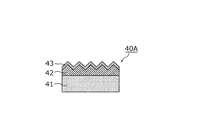
- FIG. 6A is a structural cross-sectional view of an intermediate member according to Modification 1 of the embodiment.
- FIG. 6B is a structural cross-sectional view of an intermediate member according to Modification 2 of the embodiment.
- FIG. 1 is a schematic plan view of a solar cell module according to an embodiment.
- FIG. 2 is a plan view of the solar cell element according to the embodiment.
- FIG. 3 is a cross-sectional view illustrating a stacked structure of solar cell elements according to the embodiment.
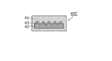
- FIG. 6C is a structural cross-sectional view of an intermediate member according to Modification 3 of the embodiment.
- FIG. 7A is a structural cross-sectional view of an intermediate member according to Modification 4 of the embodiment.
- FIG. 7B is a structural cross-sectional view of an intermediate member according to Modification 5 of the embodiment.
- FIG. 8A is a structural cross-sectional view of an intermediate member and a solar cell element according to Modification 6 of the embodiment.
- FIG. 8B is a structural cross-sectional view of an intermediate member and a solar cell element according to Modification 7 of the embodiment.
- the “front surface” of a solar cell element means a surface that allows more light to enter the interior than the “back surface” that is the opposite surface (over 50% to 100% light is the surface). And the case where no light enters the interior from the “back surface” side.
- the “surface” of the solar cell module means a surface on which light on the side facing the “surface” of the solar cell element can be incident, and the “back surface” means a surface on the opposite side.
- descriptions such as “providing the second member on the first member” do not intend only when the first and second members are provided in direct contact unless specifically limited. That is, this description includes a case where another member exists between the first and second members.
- the description of “substantially **” is intended to include not only exactly the same, but also those that are recognized as being substantially the same, with “substantially identical” as an example.
- FIG. 1 is a schematic plan view of a solar cell module according to an embodiment.
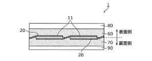
- the solar cell module 1 shown in the figure includes a plurality of solar cell elements 11, a tab wiring 20, a cross wiring 30, an intermediate member 40, and a frame body 50.
- the solar cell module 1 further includes a surface filling member, a back surface filling member, a surface protection member, and a back surface protection member.
- the solar cell elements 11 are flat-plate photovoltaic elements that are arranged in a matrix on a plane and generate power by light irradiation.
- the tab wiring 20 is a wiring member that electrically connects the solar cell elements 11 adjacent in the column direction.
- the cross wiring 30 is a wiring member for connecting the solar cell strings.
- the solar cell string is an aggregate of a plurality of solar cell elements 11 arranged in the column direction and connected by the tab wiring 20.
- the frame body 50 is an outer frame member that covers the outer periphery of a panel in which a plurality of solar cell elements 11 are two-dimensionally arranged.
- the intermediate member 40 is disposed between the solar cell elements 11 adjacent to each other in the row direction and in a region between the solar cell string and the frame body 50.
- the intermediate member 40, the surface filling member, the back surface filling member, the surface protection member, and the back surface protection member will be described in detail with reference to FIGS.
- FIG. 2 is a plan view of the solar cell element according to the embodiment.
- the solar cell element 11 has a substantially square shape in plan view.
- a plurality of striped bus bar electrodes 112 are formed in parallel to each other, and a plurality of striped finger electrodes 111 are formed in parallel to each other so as to be orthogonal to the bus bar electrodes 112. Yes.
- the bus bar electrode 112 and the finger electrode 111 constitute a collector electrode 110.
- the collector electrode 110 is formed of, for example, a conductive paste containing conductive particles such as Ag (silver).
- the line width of the bus bar electrode 112 is, for example, 1.5 mm
- the line width of the finger electrode 111 is, for example, 100 ⁇ m
- the pitch of the finger electrodes 111 is, for example, 2 mm.
- the tab wiring 20 is bonded on the bus bar electrode 112.
- FIG. 3 is a cross-sectional view showing a laminated structure of solar cell elements according to the embodiment. 2 is a CC cross-sectional view of the solar cell element 11 in FIG.
- an i-type amorphous silicon film 121 and a p-type amorphous silicon film 122 are formed in this order on the main surface of an n-type single crystal silicon wafer 101.
- the n-type single crystal silicon wafer 101, the i-type amorphous silicon film 121, and the p-type amorphous silicon film 122 form a photoelectric conversion layer, and the n-type single crystal silicon wafer 101 serves as a main power generation layer.
- the light receiving surface electrode 102 is formed on the p-type amorphous silicon film 122.
- a collecting electrode 110 including a plurality of bus bar electrodes 112 and a plurality of finger electrodes 111 is formed on the light receiving surface electrode 102.
- FIG. 3 only the finger electrode 111 of the collector electrode 110 is shown.
- an i-type amorphous silicon film 123 and an n-type amorphous silicon film 124 are formed in this order on the back surface of the n-type single crystal silicon wafer 101. Further, a light receiving surface electrode 103 is formed on the n-type amorphous silicon film 124, and a collecting electrode 110 including a plurality of bus bar electrodes 112 and a plurality of finger electrodes 111 is formed on the light receiving surface electrode 103.
- the p-type amorphous silicon layer 122 is formed on the back surface side of the n-type single crystal silicon wafer 101 and the n-type amorphous silicon layer 124 is formed on the light-receiving surface side of the n-type single crystal silicon wafer 101, respectively. Good.
- the collector electrode 110 can be formed by a printing method such as screen printing using a thermosetting resin-type conductive paste using a resin material as a binder and conductive particles such as silver particles as a filler, for example. .
- the solar cell element 11 is provided between the n-type single crystal silicon wafer 101 and the p-type amorphous silicon film 122 or the n-type amorphous silicon film 124 in order to improve the pn junction characteristics.
- the i-type amorphous silicon film 121 is provided.
- the light-receiving surface electrode 102 on the front surface side and the light-receiving surface electrode 103 on the back surface side of the n-type single crystal silicon wafer 101 are light-receiving surfaces. Carriers generated in the n-type single crystal silicon wafer 101 diffuse as photocurrents to the light-receiving surface electrodes 102 and 103 on the front surface side and the back surface side, and are collected by the collector electrode 110.
- the light receiving surface electrodes 102 and 103 are transparent electrodes made of, for example, ITO (indium tin oxide), SnO 2 (tin oxide), ZnO (zinc oxide), or the like.
- ITO indium tin oxide
- SnO 2 tin oxide
- ZnO zinc oxide
- the light receiving surface electrode 103 on the back surface side may be a metal electrode that is not transparent.
- an electrode formed on the entire surface of the light receiving surface electrode 103 may be used instead of the collector electrode 110.
- FIG. 4 is a structural cross-sectional view in the column direction of the solar cell module according to the embodiment
- FIG. 5 is a structural cross-sectional view in the row direction of the solar cell module according to the embodiment.
- FIG. 4 is a cross-sectional view taken along the line AA in FIG. 1
- FIG. 5 is a cross-sectional view taken along the line BB in the plan view of FIG.
- tab wirings 20 are arranged on the front surface and the back surface of the solar cell element 11.
- the tab wiring 20 disposed on the surface of one solar cell element 11 is also disposed on the back surface of the other solar cell element 11. More specifically, the lower surface of one end of the tab wiring 20 is joined to a bus bar electrode 112 (not shown) on the surface side of one solar cell element 11. Further, the upper surface of the other end portion of the tab wiring 20 is joined to a bus bar electrode 112 (not shown) on the back surface side of the other solar cell element 11.
- the solar cell string composed of a plurality of solar cell elements 11 arranged in the column direction has a configuration in which the plurality of solar cell elements 11 are connected in series in the column direction.
- the tab wiring 20 and the bus bar electrode 112 are joined by, for example, a resin adhesive. That is, the tab wiring 20 is connected to the solar cell element 11 through the resin adhesive.
- the resin adhesive is preferably cured at a temperature lower than the melting point of the eutectic solder, that is, about 200 ° C. or lower.
- the resin adhesive include a two-component reaction adhesive in which a curing agent is mixed with an epoxy resin, an acrylic resin, or a urethane resin, in addition to a thermosetting resin adhesive such as an acrylic resin or a highly flexible polyurethane type. Etc. can be used.
- the resin adhesive may contain a plurality of conductive particles. As such particles, nickel, nickel with gold coating, or the like can be used.
- a conductive material such as a solder coated copper foil can be used.
- a surface protection member 80 is disposed on the front surface side of the plurality of solar cell elements 11, and a back surface protection member 90 is disposed on the back surface side.
- the surface filling member 60 is arrange
- a member 70 is disposed. The front surface protection member 80 and the back surface protection member 90 are fixed by a front surface filling member 60 and a back surface filling member 70, respectively.
- the surface filling member 60 is disposed on the front surface side of the plurality of solar cell elements 11, and the back surface filling member 70 is on the back surface side of the plurality of solar cell elements 11, and a plurality of solar cells are combined with the surface filling member 60. It arrange
- the surface protection member 80 is a member that protects the inside of the solar cell module 1 from wind and rain, external impact, fire, and the like, and ensures long-term reliability of the solar cell module 1 in outdoor exposure. From this point of view, the surface protection member 80 may be made of, for example, glass having translucency and water shielding properties, a resin member having light translucency and water shielding properties such as film or plate.
- the back surface protection member 90 is a member that protects the back surface of the solar cell module 1 from the external environment, and has, for example, a resin film such as PET (Polyethylene Terephthalate) or a structure in which an Al foil is sandwiched between resin films. A laminated film or the like can be used.
- the front surface filling member 60 is a filler filled in the space between the plurality of solar cell elements 11 and the surface protection member 80, and the back surface filling member 70 is formed between the plurality of solar cell elements 11 and the back surface protection member 90. It is a filler filled in the space between.
- the front surface filling member 60 and the back surface filling member 70 have a sealing function for blocking the solar cell element 11 from the external environment. With the arrangement of the front surface filling member 60 and the back surface filling member 70, it is possible to ensure high heat resistance and high moisture resistance of the solar cell module 1 that is assumed to be installed outdoors.
- the surface filling member 60 is mainly composed of a first polyolefin material which is a polyolefin filler.
- the back surface filling member 70 is mainly composed of a second polyolefin material which is a polyolefin based filler.
- the polyolefin filler include polyethylene (polyethylene), polypropylene (polypropylene), and a polymer of polyethylene and polypropylene.
- acetic acid due to hydrolysis is not generated, and corrosion of the solar cell element 11 due to acetic acid can be suppressed.
- white particles such as titanium oxide are contained in the back surface filling member 70 in order to improve the output by utilizing reflection of light from the back surface filling member 70.
- the adhesive force at the interface between the front surface filling member 60 and the back surface filling member 70 is easily reduced compared to the case where the front surface filling member 60 and the back surface filling member 70 are the same. Is likely to occur. Therefore, when the front surface filling member 60 and the back surface filling member 70 are different, it is particularly preferable to provide the intermediate member 40 at the interface between them.
- a frame 50 made of, for example, Al is attached via an adhesive so as to surround the surface protection member 80, the back surface protection member 90, the surface filling member 60, the back surface filling member 70, and the intermediate member 40.
- solar cell module 1 is a region where solar cell element 11 is not arranged in a plan view, and includes surface filling member 60 and back surface filling member 70 in a cross-sectional view.
- An intermediate member 40 is provided at the boundary portion.
- the intermediate member 40 is sandwiched between the front surface filling member 60 and the back surface filling member 70, and is disposed outside the region where the solar cell element 11 is disposed in a plan view.
- the intermediate member 40 is mainly composed of a polymer material having a higher polarity than the first polyolefin material and the second polyolefin material.
- the intermediate member 40 is mainly composed of a polymer material having higher water absorption than the first polyolefin material and the second polyolefin material.
- the intermediate member 40 has a material that can absorb more water, which is a polar molecule, than the first polyolefin material and the second polyolefin material.
- a water absorption is mentioned as one of the physical quantities which judge the level of water absorption.
- the intermediate member 40 has, at least one of ethylene vinyl acetate (EVA) and polyethylene terephthalate is mentioned.
- EVA ethylene vinyl acetate
- the polymer material that the intermediate member 40 has include polymer materials having a hydrophilic group such as polyvinyl alcohol, ethylene-vinyl alcohol copolymer, and polyvinyl acetate.
- the above-described “polarity” can be evaluated by, for example, an SP value (Solubility Parameter) that is a solubility parameter that is a measure of the solubility of the two-component solution. From the evaluation of the solubility parameter, it can be determined that the solubility of the two components is higher as the difference between the SP values of the two components is smaller. If this is applied to the present embodiment, it can be determined that a material having an SP value closer to the SP value of water is more likely to dissolve water. From this point of view, the polymer material of the intermediate member 40 is more polar than the first polyolefin material and the second polyolefin material. The SP value of the polymer material is the first polyolefin material and the second polyolefin.
- SP value of the polymer material is the first polyolefin material and the second polyolefin.
- the SP value of water which is a polar substance
- the SP value of the system material is closer to the SP value of the system material.
- the first polyolefin material and the second polyolefin material are polyethylene and the polymer material of the intermediate member 40 is polyethylene terephthalate.
- the SP value (theoretical value) of water is 23.4
- the SP value of polyethylene is 7.9
- the SP value of polyethylene terephthalate is 10.7. That is, the difference in SP value between water and polyethylene is 15.5, whereas the difference in SP value between water and polyethylene terephthalate is 12.7.
- the SP value (10.7) of polyethylene terephthalate is closer to the SP value (23.4) of water than the SP value (7.9) of polyethylene. Therefore, it is determined that polyethylene terephthalate has a higher polarity than polyethylene.
- the surface between the surface filling member 60 and the back surface filling member 70 can be obtained even if the inherent moisture is vaporized due to a rapid temperature change.
- the intermediate member 40 disposed in contact with the filling member 60 and the back surface filling member 70 absorbs the vaporized water. Thereby, the intermediate member 40 does not expand in volume, and it becomes possible to suppress the expansion (volume expansion) and the generation of bubbles at the interface between the front surface filling member 60 and the back surface filling member 70.
- the intermediate member 40 is installed in at least a part between the front surface filling member 60 and the back surface filling member 70 corresponding to the interface between the front surface filling member 60 and the back surface filling member 70 configured when the intermediate member 40 is not installed. It is preferable that it is installed between the areas corresponding to almost the entire area of the interface.
- the priority of the installation position of the intermediate member 40 is (1) installation between solar cell strings, (2) installation between solar cell elements 11, and (3) arrangement on the outer periphery of the solar cell element 11.
- the intermediate member 40 was set as the structure arrange
- the intermediate member 40 according to the present embodiment is a member mainly composed of a polymer material having a higher polarity or higher water absorption than the first polyolefin material and the second polyolefin material. Furthermore, it is a region where the solar cell element 11 is not disposed in plan view, and is disposed at the interface between the front surface filling member 60 and the back surface filling member 70. That is, the intermediate member 40 may have a structure that satisfies these materials and arrangement.
- it is desirable that the intermediate member according to the present embodiment not only has excellent water absorption and hygroscopicity as described above, but also has a light diffusion and light reflection function.
- modifications 1 to 7 show a configuration in which the intermediate member according to the present embodiment further has a light diffusion and light reflection function.
- FIG. 6A is a structural cross-sectional view of an intermediate member according to Modification 1 of the embodiment. 6A and FIGS. 6B to 8B described below show cross-sectional views when the intermediate member disposed between the solar cell elements 11 adjacent in the row direction is cut in the row direction.
- the intermediate member 40A shown in FIG. 6A includes a first polymer layer 41, a second polymer layer 42, and a metal layer 43.
- the first polymer layer 41 has a bottom surface that is in contact with the back surface filling member 70, and is mainly composed of a polymer material having higher polarity or higher water absorption than the first polyolefin material and the second polyolefin material. It is a member.
- ethylene vinyl acetate (EVA) is suitable as the polymer material that the first polymer layer 41 has.
- the second polymer layer 42 is a member that is formed on the surface of the first polymer layer 41 and has as a main component a polymer material that is harder than the polymer material that the first polymer layer 41 has.
- the second polymer layer 42 has a plurality of irregularities.
- a hard polymer material as the material of the second polymer layer 42, the controllability of the surface processing of the second polymer layer 42 is improved, and the accuracy of the uneven shape can be increased.
- PET polyethylene terephthalate
- the metal layer 43 is a metal member formed on the surface of the second polymer layer 42, and the surface not in contact with the second polymer layer 42 is in contact with the surface filling member 60.
- the metal layer 43 is preferably made of Al having a high reflectance with respect to light, for example.
- the metal layer 43 has a plurality of irregularities. Thereby, light incident from the surface side is reflected in multiple directions on the surface of the metal layer 43. That is, the intermediate member 40A has a light diffusion and light reflection function. Therefore, since light that does not directly enter the solar cell element 11 can be redistributed to the solar cell element 11, it is possible to improve the photoelectric conversion efficiency of the entire solar cell module.
- the intermediate member 40 ⁇ / b> A absorbs the evaporated water by the first polymer layer 41. Accordingly, the intermediate member 40A does not expand in volume, and it is possible to suppress the expansion (volume expansion) and the generation of bubbles at the interface between the front surface filling member 60 and the back surface filling member 70. Therefore, it becomes possible to improve the photoelectric conversion efficiency of the entire solar cell module, in addition to preventing corrosion of the solar cell element 11 and suppressing swelling and peeling.
- FIG. 6B is a structural cross-sectional view of an intermediate member according to Modification 2 of the embodiment.
- the intermediate member 40B shown in the figure is the same as the intermediate member 40A according to the modified example 1 in that the first polymer layer 41, the second polymer layer 42, and the metal layer 43 are provided.
- the stacking relationship (order) is different.
- the description of the same points as those of the first modification will be omitted, and only differences from the configuration will be described.
- the second polymer layer 42 is a member whose bottom is in contact with the back surface filling member 70 and whose main component is a polymer material that is harder than the polymer material that the first polymer layer 41 has.
- the metal layer 43 is a metal member formed on the surface of the second polymer layer 42.
- the first polymer layer 41 is formed on the surface of the metal layer 43 and is a member mainly composed of a polymer material having a higher polarity or higher water absorption than the first polyolefin material and the second polyolefin material. It is.
- the metal layer 43 has a plurality of irregularities.
- the intermediate member 40B has a light diffusion and light reflection function. Therefore, since light that is not directly incident on the solar cell element 11 can be redistributed to the solar cell element 11, the photoelectric conversion efficiency as the solar cell module 1 can be improved.
- the intermediate member 40 ⁇ / b> B absorbs vaporized water by the first polymer layer 41. Accordingly, the intermediate member 40B does not expand in volume, and it is possible to suppress the expansion (volume expansion) and the generation of bubbles at the interface between the front surface filling member 60 and the back surface filling member 70. Therefore, it becomes possible to improve the photoelectric conversion efficiency of the entire solar cell module, in addition to preventing corrosion of the solar cell element 11 and suppressing swelling and peeling.
- FIG. 6C is a structural cross-sectional view of an intermediate member according to Modification 3 of the embodiment.
- the intermediate member 40 ⁇ / b> C shown in the figure is the same as the intermediate member 40 ⁇ / b> B according to Modification 2 in that the first polymer layer 41, the second polymer layer 42, and the metal layer 43 are provided.
- the formation range of the first polymer layer 41 is different.
- the description of the same points as those of the modified example 2 will be omitted, and only differences from the configuration will be described.
- the second polymer layer 42 is a member whose bottom is in contact with the first polymer layer 41 and whose main component is a polymer material that is harder than the polymer material that the first polymer layer 41 has.
- the metal layer 43 is a metal member formed on the surface of the second polymer layer 42.
- the first polymer layer 41 is formed so as to cover the second polymer layer 42 and the metal layer 43, and has a higher polarity or higher water absorption than the first polyolefin material and the second polyolefin material. It is a member mainly composed of materials.
- the metal layer 43 has a plurality of irregularities.
- the intermediate member 40C has a light diffusion and light reflection function. Therefore, since light that does not directly enter the solar cell element 11 can be redistributed to the solar cell element 11, it is possible to improve the photoelectric conversion efficiency of the entire solar cell module.
- the intermediate member 40 ⁇ / b> C absorbs vaporized water by the first polymer layer 41. Accordingly, the intermediate member 40C does not expand in volume, and it is possible to suppress the expansion (volume expansion) and the generation of bubbles at the interface between the front surface filling member 60 and the back surface filling member 70. Therefore, it becomes possible to improve the photoelectric conversion efficiency of the entire solar cell module, in addition to preventing corrosion of the solar cell element 11 and suppressing swelling and peeling.
- the intermediate member 40C has a structure in which the metal layer 43 is covered with the first polymer layer 41, the same polarity of the solar cell elements 11 adjacent to each other with the intermediate member 40C interposed therebetween is interposed between the metal layer 43. Can be prevented from short-circuiting.
- the same polarity of the adjacent solar cell elements 11 is short-circuited by limiting the formation region of the metal layer 43. The possibility of doing so can be eliminated.
- FIG. 7A is a structural cross-sectional view of an intermediate member according to Modification 4 of the embodiment.
- the intermediate member 40D shown in the figure is the same as the intermediate member 40A according to the modified example 1 in that the first polymer layer 41, the second polymer layer 42, and the metal layer 43 are provided. Only the formation range of the metal layer 43 is different.
- the description of the same points as those of the first modification will be omitted, and only differences from the configuration will be described.
- the metal layer 43 is a metal member formed on the surface of the second polymer layer 42.
- the metal layer 43 is not formed up to the end surface of the second polymer layer 42. That is, the second polymer layer 42 has an end surface on which the metal layer 43 is not formed. Thereby, it can prevent that the same polarity of the solar cell element 11 adjacent on both sides of intermediate member 40D short-circuits via the metal layer 43.
- FIG. 7B is a structural cross-sectional view of an intermediate member according to Modification 5 of the embodiment.
- the intermediate member 40E shown in the figure is the same as the intermediate member 40B according to the modified example 2 in that the first polymer layer 41, the second polymer layer 42, and the metal layer 43 are provided. Only the formation range of the metal layer 43 is different.
- the description of the same points as those of the modified example 2 will be omitted, and only differences from the configuration will be described.
- the metal layer 43 is a metal member formed on the surface of the second polymer layer 42.
- the metal layer 43 is not formed up to the end surface of the second polymer layer 42. That is, the second polymer layer 42 has an end surface on which the metal layer 43 is not formed. Thereby, it can prevent that the same polarity of the solar cell element 11 adjacent on both sides of the intermediate member 40E short-circuits via the metal layer 43.
- the metal layer 43 and the second polymer layer 42 shown in FIGS. 6A, 6B, 6C, 7A, and 7B have regular irregular shapes, but the irregular shapes are random. It may be a shape.
- the surface of the 2nd polymer layer 42 shown by FIG. 6A, FIG. 6B, FIG. 6C, FIG. 7A, and FIG. 7B has uneven
- the 2nd polymer layer 42 The surface may be flat and the metal layer 43 may have a concavo-convex shape only. In this case, what is necessary is just to adjust the thickness of the metal layer 43 according to required uneven
- the intermediate member shown by FIG. 6A, FIG. 6B, FIG. 6C, FIG. 7A, and FIG. 7B is the structure provided with the metal layer 43, it is not restricted to this, It is the structure in which the metal layer 43 is not formed. There may be. Even with this configuration, it is possible to have a light diffusion function.
- the intermediate member shown in FIGS. 6A, 6B, 6C, 7A, and 7B may have a configuration without an uneven shape.
- the surface of the metal layer 43 is preferably roughened. This makes it possible to have a light diffusion function.
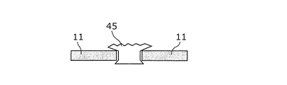
- FIG. 8A is a structural cross-sectional view of an intermediate member and a solar cell element according to Modification 6 of the embodiment.
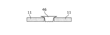
- FIG. 8B is a structural cross-sectional view of the intermediate member and the solar cell element according to Modification 7 of the embodiment. 8A and 8B show cross sections of two adjacent solar cell elements 11 and intermediate members 45 and 46 disposed between them.
- the intermediate member 45 shown in FIG. 8A has a shape in which the area of the front surface and the back surface is larger than the area of the cross section parallel to the front surface and the back surface in the central portion between the front surface and the back surface. With this shape, the intermediate member 45 can be prevented from shifting in the vertical direction in the step of arranging the intermediate member.
- the intermediate member 46 shown in FIG. 8B has a front surface wider than the back surface, a front surface width greater than the distance between two adjacent solar cell elements 11, and a back surface width between the two adjacent solar cell elements 11. It has a smaller shape. That is, the cross-sectional shape of the intermediate member 46 cut in the row direction has a substantially trapezoidal shape in which the upper base is longer than the lower base. With this shape, it is possible to suppress the intermediate member 46 from falling downward in the step of arranging the intermediate member.
- the intermediate member 45 according to Modification 6 and the intermediate member 46 according to Modification 7 it is not necessary to bond the intermediate member to the adjacent solar cell elements 11 using an adhesive or the like. Therefore, it becomes possible to manufacture a solar cell module having an intermediate member arranged with high accuracy at low cost.
- the intermediate member 45 shown in FIG. 8A has a plurality of uneven shapes on the surface
- the intermediate member 46 shown in FIG. 8B has a plurality of uneven shapes on the back surface.
- the intermediate members 45 and 46 have a light diffusion and light reflection function.
- the laminated structure of the intermediate members according to the modified examples 1 to 5 is applied.
- intermediate members 45 and 46 may have a structure not having a plurality of uneven shapes as a structure not having a light diffusion function.
- the solar cell module 1 includes a plurality of solar cell elements 11, a surface filling member 60 including a first polyolefin-based material, disposed on the surface side of the plurality of solar cell elements 11, and a plurality of solar cells.
- the back surface filling member 70 including the second polyolefin-based material disposed on the back surface side of the battery element 11 is disposed at the interface between the front surface filling member 60 and the back surface filling member 70, and the solar cell element 11 is disposed in plan view.
- An intermediate member that is disposed outside the region and includes a polymer material having a higher polarity than the first polyolefin material and the second polyolefin material, or having a higher water absorption than the first polyolefin material and the second polyolefin material. 40 and the plurality of solar cell elements 11, the surface protection member 80 disposed so as to sandwich the surface filling member 60, and the plurality of solar cell elements 11 Hama and a back surface protective member 90 disposed so as to sandwich the member 70.
- the intermediate member 40 disposed at the interface between the front surface filling member 60 and the back surface filling member 70 absorbs the vaporized water.
- the intermediate member 40 does not expand in volume, and it becomes possible to suppress the expansion (volume expansion) and the generation of bubbles at the interface between the front surface filling member 60 and the back surface filling member 70. Therefore, corrosion of the solar cell element 11 is prevented by the surface filling member 60 having the first polyolefin-based material as the main component and the back surface filling member 70 having the second polyolefin-based material as the main component, and the intermediate member 40 swells and It becomes possible to suppress peeling.
- a plurality of irregularities may be formed on the surface of the intermediate member.
- the light incident from the surface side diffuses on the surface of the intermediate member. Therefore, since light that does not directly enter the solar cell element 11 can be redistributed to the solar cell element 11, it is possible to improve the photoelectric conversion efficiency of the entire solar cell module.
- the intermediate member includes a first polymer layer 41 mainly composed of a polymer material, a second polymer layer 42 mainly composed of a polymer material harder than the polymer material, A metal layer 43 formed on the surface of the polymer layer 42 may be provided.
- the second polymer layer 42 and the metal layer 43 may have a plurality of irregularities.
- the second polymer layer 42 may be formed on the first polymer layer 41.
- the first polymer layer 41 may be formed on the metal layer 43.
- the first polymer layer 41 may be formed so as to cover the metal layer 43 and the second polymer layer 42.
- the polymer material that is the main component of the first polymer layer 41 may be ethylene vinyl acetate
- the polymer material that is the main component of the second polymer layer 42 may be polyethylene terephthalate.
- the solar cell element 11 only needs to have a function as a photovoltaic power, and is not limited to the structure of the solar cell element.
- a light diffusing member may be formed on the tab wiring 20 and the cross wiring 30 so as to cover the upper surfaces of the tab wiring 20 and the cross wiring 30.
- the embodiment can be realized by arbitrarily combining the components and functions in each embodiment without departing from the scope of the present invention, or a form obtained by subjecting each embodiment to various modifications conceived by those skilled in the art. Forms are also included in the present invention.
Landscapes
- Engineering & Computer Science (AREA)
- Physics & Mathematics (AREA)
- Condensed Matter Physics & Semiconductors (AREA)
- Electromagnetism (AREA)
- General Physics & Mathematics (AREA)
- Computer Hardware Design (AREA)
- Microelectronics & Electronic Packaging (AREA)
- Power Engineering (AREA)
- Life Sciences & Earth Sciences (AREA)
- Sustainable Energy (AREA)
- Photovoltaic Devices (AREA)
Abstract
Priority Applications (4)
| Application Number | Priority Date | Filing Date | Title |
|---|---|---|---|
| EP15810466.1A EP3159936A4 (fr) | 2014-06-18 | 2015-06-12 | Module de cellule solaire |
| JP2016529033A JP6590261B2 (ja) | 2014-06-18 | 2015-06-12 | 太陽電池モジュール |
| US15/381,040 US10074759B2 (en) | 2014-06-18 | 2016-12-15 | Solar cell module |
| US16/045,693 US20180331243A1 (en) | 2014-06-18 | 2018-07-25 | Solar cell module |
Applications Claiming Priority (2)
| Application Number | Priority Date | Filing Date | Title |
|---|---|---|---|
| JP2014-125779 | 2014-06-18 | ||
| JP2014125779 | 2014-06-18 |
Related Child Applications (1)
| Application Number | Title | Priority Date | Filing Date |
|---|---|---|---|
| US15/381,040 Continuation US10074759B2 (en) | 2014-06-18 | 2016-12-15 | Solar cell module |
Publications (1)
| Publication Number | Publication Date |
|---|---|
| WO2015194146A1 true WO2015194146A1 (fr) | 2015-12-23 |
Family
ID=54935153
Family Applications (1)
| Application Number | Title | Priority Date | Filing Date |
|---|---|---|---|
| PCT/JP2015/002955 WO2015194146A1 (fr) | 2014-06-18 | 2015-06-12 | Module de cellule solaire |
Country Status (4)
| Country | Link |
|---|---|
| US (2) | US10074759B2 (fr) |
| EP (1) | EP3159936A4 (fr) |
| JP (1) | JP6590261B2 (fr) |
| WO (1) | WO2015194146A1 (fr) |
Cited By (1)
| Publication number | Priority date | Publication date | Assignee | Title |
|---|---|---|---|---|
| WO2019205920A1 (fr) * | 2018-04-27 | 2019-10-31 | Global Solar Energy, Inc. | Dispositifs photovoltaïques comprenant des pixels bicouches ayant des propriétés réfléchissantes et/ou antireflet |
Families Citing this family (2)
| Publication number | Priority date | Publication date | Assignee | Title |
|---|---|---|---|---|
| JP1618129S (fr) * | 2018-03-28 | 2018-11-19 | ||
| JP6924887B1 (ja) * | 2020-11-02 | 2021-08-25 | ジョジアン ジンコ ソーラー カンパニー リミテッド | 光起電力モジュール |
Citations (6)
| Publication number | Priority date | Publication date | Assignee | Title |
|---|---|---|---|---|
| WO2011093383A1 (fr) * | 2010-01-29 | 2011-08-04 | 三洋電機株式会社 | Module de cellules solaires |
| WO2012053042A1 (fr) * | 2010-10-19 | 2012-04-26 | Fujifilm Corporation | Module de cellule solaire et son procédé de fabrication |
| WO2012073751A1 (fr) * | 2010-11-30 | 2012-06-07 | 三洋電機株式会社 | Module de pile solaire et son procédé de production |
| JP2013012589A (ja) * | 2011-06-29 | 2013-01-17 | Sanyo Electric Co Ltd | 太陽電池モジュール |
| JP2013125778A (ja) * | 2011-12-13 | 2013-06-24 | Fuji Electric Co Ltd | 太陽電池モジュールおよびその製造方法 |
| JP2014007384A (ja) * | 2012-06-22 | 2014-01-16 | Lg Electronics Inc | 太陽電池モジュール及びそれに適用されるリボン結合体 |
Family Cites Families (8)
| Publication number | Priority date | Publication date | Assignee | Title |
|---|---|---|---|---|
| US5994641A (en) * | 1998-04-24 | 1999-11-30 | Ase Americas, Inc. | Solar module having reflector between cells |
| US20030000568A1 (en) * | 2001-06-15 | 2003-01-02 | Ase Americas, Inc. | Encapsulated photovoltaic modules and method of manufacturing same |
| JP4974472B2 (ja) * | 2005-03-30 | 2012-07-11 | 三洋電機株式会社 | 太陽電池モジュール及びこれを備えた太陽電池装置 |
| JP4662151B2 (ja) | 2005-11-29 | 2011-03-30 | 大日本印刷株式会社 | 太陽電池モジュール用充填材、およびそれを用いた太陽電池モジュール、ならびに太陽電池モジュール用充填材の製造方法 |
| CN102664210B (zh) * | 2012-05-14 | 2015-05-06 | 友达光电股份有限公司 | 太阳能模块与其制造方法 |
| KR101988873B1 (ko) * | 2012-06-14 | 2019-06-14 | 주식회사 쿠라레 | 다층 구조체 및 이를 사용한 디바이스, 및 이들의 제조 방법 |
| CN102800730A (zh) * | 2012-07-09 | 2012-11-28 | 友达光电股份有限公司 | 光伏装置 |
| JPWO2014033802A1 (ja) * | 2012-08-27 | 2016-08-08 | パナソニックIpマネジメント株式会社 | 太陽電池モジュール |
-
2015
- 2015-06-12 WO PCT/JP2015/002955 patent/WO2015194146A1/fr active Application Filing
- 2015-06-12 JP JP2016529033A patent/JP6590261B2/ja active Active
- 2015-06-12 EP EP15810466.1A patent/EP3159936A4/fr not_active Withdrawn
-
2016
- 2016-12-15 US US15/381,040 patent/US10074759B2/en active Active
-
2018
- 2018-07-25 US US16/045,693 patent/US20180331243A1/en not_active Abandoned
Patent Citations (6)
| Publication number | Priority date | Publication date | Assignee | Title |
|---|---|---|---|---|
| WO2011093383A1 (fr) * | 2010-01-29 | 2011-08-04 | 三洋電機株式会社 | Module de cellules solaires |
| WO2012053042A1 (fr) * | 2010-10-19 | 2012-04-26 | Fujifilm Corporation | Module de cellule solaire et son procédé de fabrication |
| WO2012073751A1 (fr) * | 2010-11-30 | 2012-06-07 | 三洋電機株式会社 | Module de pile solaire et son procédé de production |
| JP2013012589A (ja) * | 2011-06-29 | 2013-01-17 | Sanyo Electric Co Ltd | 太陽電池モジュール |
| JP2013125778A (ja) * | 2011-12-13 | 2013-06-24 | Fuji Electric Co Ltd | 太陽電池モジュールおよびその製造方法 |
| JP2014007384A (ja) * | 2012-06-22 | 2014-01-16 | Lg Electronics Inc | 太陽電池モジュール及びそれに適用されるリボン結合体 |
Non-Patent Citations (1)
| Title |
|---|
| See also references of EP3159936A4 * |
Cited By (1)
| Publication number | Priority date | Publication date | Assignee | Title |
|---|---|---|---|---|
| WO2019205920A1 (fr) * | 2018-04-27 | 2019-10-31 | Global Solar Energy, Inc. | Dispositifs photovoltaïques comprenant des pixels bicouches ayant des propriétés réfléchissantes et/ou antireflet |
Also Published As
| Publication number | Publication date |
|---|---|
| JP6590261B2 (ja) | 2019-10-16 |
| EP3159936A4 (fr) | 2017-06-14 |
| JPWO2015194146A1 (ja) | 2017-04-20 |
| EP3159936A1 (fr) | 2017-04-26 |
| US20170098725A1 (en) | 2017-04-06 |
| US10074759B2 (en) | 2018-09-11 |
| US20180331243A1 (en) | 2018-11-15 |
Similar Documents
| Publication | Publication Date | Title |
|---|---|---|
| JP6526774B2 (ja) | 太陽電池モジュール | |
| JP6624418B2 (ja) | 太陽電池モジュール | |
| WO2013168612A1 (fr) | Module de cellule solaire | |
| EP3067937B1 (fr) | Module de cellule solaire | |
| JP6709977B2 (ja) | 太陽電池モジュール | |
| US20170373210A1 (en) | Solar cell module | |
| US20180331243A1 (en) | Solar cell module | |
| US20170365727A1 (en) | Solar cell module | |
| WO2017002287A1 (fr) | Module de batterie solaire | |
| JP2006278695A (ja) | 太陽電池モジュール | |
| JPWO2020054130A1 (ja) | 太陽電池モジュール | |
| TWM502963U (zh) | 太陽能電池模組 | |
| KR101616131B1 (ko) | 태양전지 모듈 | |
| US10784384B2 (en) | Solar cell module | |
| WO2015194147A1 (fr) | Module à cellule solaire | |
| JP6025123B2 (ja) | 太陽電池モジュール | |
| JP2017050514A (ja) | 太陽電池モジュール | |
| JP6771200B2 (ja) | 太陽電池モジュール | |
| JP2016192436A (ja) | 太陽電池モジュール | |
| JP5906422B2 (ja) | 太陽電池及び太陽電池モジュール | |
| JP2018056454A (ja) | 太陽電池モジュール及び太陽電池モジュールの製造方法 | |
| JP6495650B2 (ja) | 太陽電池モジュールおよびこれを用いた太陽電池アレイ | |
| JP6528196B2 (ja) | 太陽電池モジュール | |
| JP7483382B2 (ja) | 太陽電池モジュール | |
| WO2023127382A1 (fr) | Dispositif de photopiles et module de photopile |
Legal Events
| Date | Code | Title | Description |
|---|---|---|---|
| 121 | Ep: the epo has been informed by wipo that ep was designated in this application |
Ref document number: 15810466 Country of ref document: EP Kind code of ref document: A1 |
|
| ENP | Entry into the national phase |
Ref document number: 2016529033 Country of ref document: JP Kind code of ref document: A |
|
| REEP | Request for entry into the european phase |
Ref document number: 2015810466 Country of ref document: EP |
|
| WWE | Wipo information: entry into national phase |
Ref document number: 2015810466 Country of ref document: EP |
|
| NENP | Non-entry into the national phase |
Ref country code: DE |