JP6590261B2 - 太陽電池モジュール - Google Patents
太陽電池モジュール Download PDFInfo
- Publication number
- JP6590261B2 JP6590261B2 JP2016529033A JP2016529033A JP6590261B2 JP 6590261 B2 JP6590261 B2 JP 6590261B2 JP 2016529033 A JP2016529033 A JP 2016529033A JP 2016529033 A JP2016529033 A JP 2016529033A JP 6590261 B2 JP6590261 B2 JP 6590261B2
- Authority
- JP
- Japan
- Prior art keywords
- solar cell
- polymer layer
- back surface
- intermediate member
- filling member
- Prior art date
- Legal status (The legal status is an assumption and is not a legal conclusion. Google has not performed a legal analysis and makes no representation as to the accuracy of the status listed.)
- Active
Links
- 229920000642 polymer Polymers 0.000 claims description 76
- 239000000463 material Substances 0.000 claims description 56
- 229910052751 metal Inorganic materials 0.000 claims description 53
- 239000002184 metal Substances 0.000 claims description 53
- 229920000098 polyolefin Polymers 0.000 claims description 50
- 239000002861 polymer material Substances 0.000 claims description 29
- XLYOFNOQVPJJNP-UHFFFAOYSA-N water Substances O XLYOFNOQVPJJNP-UHFFFAOYSA-N 0.000 claims description 26
- -1 polyethylene terephthalate Polymers 0.000 claims description 24
- 239000005020 polyethylene terephthalate Substances 0.000 claims description 12
- 229920000139 polyethylene terephthalate Polymers 0.000 claims description 12
- 238000010521 absorption reaction Methods 0.000 claims description 11
- 239000005038 ethylene vinyl acetate Substances 0.000 claims description 4
- DQXBYHZEEUGOBF-UHFFFAOYSA-N but-3-enoic acid;ethene Chemical group C=C.OC(=O)CC=C DQXBYHZEEUGOBF-UHFFFAOYSA-N 0.000 claims description 2
- 229920001200 poly(ethylene-vinyl acetate) Polymers 0.000 claims description 2
- 230000004048 modification Effects 0.000 description 22
- 238000012986 modification Methods 0.000 description 22
- 239000000945 filler Substances 0.000 description 21
- 229910021417 amorphous silicon Inorganic materials 0.000 description 13
- 239000004698 Polyethylene Substances 0.000 description 11
- 238000006243 chemical reaction Methods 0.000 description 11
- 229920000573 polyethylene Polymers 0.000 description 11
- QTBSBXVTEAMEQO-UHFFFAOYSA-N Acetic acid Chemical compound CC(O)=O QTBSBXVTEAMEQO-UHFFFAOYSA-N 0.000 description 10
- 239000000853 adhesive Substances 0.000 description 10
- 230000001070 adhesive effect Effects 0.000 description 10
- 229920005989 resin Polymers 0.000 description 10
- 239000011347 resin Substances 0.000 description 10
- 238000005260 corrosion Methods 0.000 description 9
- 230000007797 corrosion Effects 0.000 description 9
- 238000009792 diffusion process Methods 0.000 description 9
- 229910021421 monocrystalline silicon Inorganic materials 0.000 description 9
- 230000008961 swelling Effects 0.000 description 7
- 239000002245 particle Substances 0.000 description 6
- 230000008859 change Effects 0.000 description 5
- PXHVJJICTQNCMI-UHFFFAOYSA-N Nickel Chemical compound [Ni] PXHVJJICTQNCMI-UHFFFAOYSA-N 0.000 description 4
- XLOMVQKBTHCTTD-UHFFFAOYSA-N Zinc monoxide Chemical compound [Zn]=O XLOMVQKBTHCTTD-UHFFFAOYSA-N 0.000 description 4
- 230000015572 biosynthetic process Effects 0.000 description 4
- 239000004743 Polypropylene Substances 0.000 description 3
- 239000000470 constituent Substances 0.000 description 3
- 238000009434 installation Methods 0.000 description 3
- 229920001155 polypropylene Polymers 0.000 description 3
- 239000004925 Acrylic resin Substances 0.000 description 2
- 229920000178 Acrylic resin Polymers 0.000 description 2
- BQCADISMDOOEFD-UHFFFAOYSA-N Silver Chemical compound [Ag] BQCADISMDOOEFD-UHFFFAOYSA-N 0.000 description 2
- 230000007062 hydrolysis Effects 0.000 description 2
- 238000006460 hydrolysis reaction Methods 0.000 description 2
- 230000001788 irregular Effects 0.000 description 2
- 238000004519 manufacturing process Methods 0.000 description 2
- 238000000034 method Methods 0.000 description 2
- 229910052759 nickel Inorganic materials 0.000 description 2
- 230000001681 protective effect Effects 0.000 description 2
- 229910052709 silver Inorganic materials 0.000 description 2
- 239000004332 silver Substances 0.000 description 2
- 229910000679 solder Inorganic materials 0.000 description 2
- 239000000758 substrate Substances 0.000 description 2
- 229920001187 thermosetting polymer Polymers 0.000 description 2
- 239000011787 zinc oxide Substances 0.000 description 2
- RYGMFSIKBFXOCR-UHFFFAOYSA-N Copper Chemical compound [Cu] RYGMFSIKBFXOCR-UHFFFAOYSA-N 0.000 description 1
- 229920000219 Ethylene vinyl alcohol Polymers 0.000 description 1
- 239000004372 Polyvinyl alcohol Substances 0.000 description 1
- 229910006404 SnO 2 Inorganic materials 0.000 description 1
- GWEVSGVZZGPLCZ-UHFFFAOYSA-N Titan oxide Chemical compound O=[Ti]=O GWEVSGVZZGPLCZ-UHFFFAOYSA-N 0.000 description 1
- 239000011230 binding agent Substances 0.000 description 1
- 230000000903 blocking effect Effects 0.000 description 1
- 239000000969 carrier Substances 0.000 description 1
- 239000003795 chemical substances by application Substances 0.000 description 1
- 239000011248 coating agent Substances 0.000 description 1
- 238000000576 coating method Methods 0.000 description 1
- 239000004020 conductor Substances 0.000 description 1
- 239000011889 copper foil Substances 0.000 description 1
- 238000002425 crystallisation Methods 0.000 description 1
- 230000008025 crystallization Effects 0.000 description 1
- 238000010586 diagram Methods 0.000 description 1
- 230000000694 effects Effects 0.000 description 1
- 239000003822 epoxy resin Substances 0.000 description 1
- 230000005496 eutectics Effects 0.000 description 1
- 238000011156 evaluation Methods 0.000 description 1
- 239000011888 foil Substances 0.000 description 1
- 239000011521 glass Substances 0.000 description 1
- PCHJSUWPFVWCPO-UHFFFAOYSA-N gold Chemical compound [Au] PCHJSUWPFVWCPO-UHFFFAOYSA-N 0.000 description 1
- 229910052737 gold Inorganic materials 0.000 description 1
- 239000010931 gold Substances 0.000 description 1
- AMGQUBHHOARCQH-UHFFFAOYSA-N indium;oxotin Chemical compound [In].[Sn]=O AMGQUBHHOARCQH-UHFFFAOYSA-N 0.000 description 1
- 230000007774 longterm Effects 0.000 description 1
- 239000011159 matrix material Substances 0.000 description 1
- 230000008018 melting Effects 0.000 description 1
- 238000002844 melting Methods 0.000 description 1
- 230000002093 peripheral effect Effects 0.000 description 1
- 229920000647 polyepoxide Polymers 0.000 description 1
- 229920002635 polyurethane Polymers 0.000 description 1
- 239000004814 polyurethane Substances 0.000 description 1
- 239000011118 polyvinyl acetate Substances 0.000 description 1
- 229920002689 polyvinyl acetate Polymers 0.000 description 1
- 229920002451 polyvinyl alcohol Polymers 0.000 description 1
- 238000010248 power generation Methods 0.000 description 1
- 238000007639 printing Methods 0.000 description 1
- 230000008569 process Effects 0.000 description 1
- 238000007650 screen-printing Methods 0.000 description 1
- 238000007789 sealing Methods 0.000 description 1
- 239000000126 substance Substances 0.000 description 1
- 229920002803 thermoplastic polyurethane Polymers 0.000 description 1
- XOLBLPGZBRYERU-UHFFFAOYSA-N tin dioxide Chemical compound O=[Sn]=O XOLBLPGZBRYERU-UHFFFAOYSA-N 0.000 description 1
- 229910001887 tin oxide Inorganic materials 0.000 description 1
- OGIDPMRJRNCKJF-UHFFFAOYSA-N titanium oxide Inorganic materials [Ti]=O OGIDPMRJRNCKJF-UHFFFAOYSA-N 0.000 description 1
- 230000009466 transformation Effects 0.000 description 1
Images


Classifications
-
- H—ELECTRICITY
- H01—ELECTRIC ELEMENTS
- H01L—SEMICONDUCTOR DEVICES NOT COVERED BY CLASS H10
- H01L31/00—Semiconductor devices sensitive to infrared radiation, light, electromagnetic radiation of shorter wavelength or corpuscular radiation and specially adapted either for the conversion of the energy of such radiation into electrical energy or for the control of electrical energy by such radiation; Processes or apparatus specially adapted for the manufacture or treatment thereof or of parts thereof; Details thereof
- H01L31/04—Semiconductor devices sensitive to infrared radiation, light, electromagnetic radiation of shorter wavelength or corpuscular radiation and specially adapted either for the conversion of the energy of such radiation into electrical energy or for the control of electrical energy by such radiation; Processes or apparatus specially adapted for the manufacture or treatment thereof or of parts thereof; Details thereof adapted as photovoltaic [PV] conversion devices
- H01L31/042—PV modules or arrays of single PV cells
- H01L31/048—Encapsulation of modules
- H01L31/0481—Encapsulation of modules characterised by the composition of the encapsulation material
-
- H—ELECTRICITY
- H01—ELECTRIC ELEMENTS
- H01L—SEMICONDUCTOR DEVICES NOT COVERED BY CLASS H10
- H01L31/00—Semiconductor devices sensitive to infrared radiation, light, electromagnetic radiation of shorter wavelength or corpuscular radiation and specially adapted either for the conversion of the energy of such radiation into electrical energy or for the control of electrical energy by such radiation; Processes or apparatus specially adapted for the manufacture or treatment thereof or of parts thereof; Details thereof
- H01L31/04—Semiconductor devices sensitive to infrared radiation, light, electromagnetic radiation of shorter wavelength or corpuscular radiation and specially adapted either for the conversion of the energy of such radiation into electrical energy or for the control of electrical energy by such radiation; Processes or apparatus specially adapted for the manufacture or treatment thereof or of parts thereof; Details thereof adapted as photovoltaic [PV] conversion devices
- H01L31/042—PV modules or arrays of single PV cells
- H01L31/048—Encapsulation of modules
-
- H—ELECTRICITY
- H01—ELECTRIC ELEMENTS
- H01L—SEMICONDUCTOR DEVICES NOT COVERED BY CLASS H10
- H01L31/00—Semiconductor devices sensitive to infrared radiation, light, electromagnetic radiation of shorter wavelength or corpuscular radiation and specially adapted either for the conversion of the energy of such radiation into electrical energy or for the control of electrical energy by such radiation; Processes or apparatus specially adapted for the manufacture or treatment thereof or of parts thereof; Details thereof
- H01L31/04—Semiconductor devices sensitive to infrared radiation, light, electromagnetic radiation of shorter wavelength or corpuscular radiation and specially adapted either for the conversion of the energy of such radiation into electrical energy or for the control of electrical energy by such radiation; Processes or apparatus specially adapted for the manufacture or treatment thereof or of parts thereof; Details thereof adapted as photovoltaic [PV] conversion devices
- H01L31/054—Optical elements directly associated or integrated with the PV cell, e.g. light-reflecting means or light-concentrating means
- H01L31/0547—Optical elements directly associated or integrated with the PV cell, e.g. light-reflecting means or light-concentrating means comprising light concentrating means of the reflecting type, e.g. parabolic mirrors, concentrators using total internal reflection
-
- H—ELECTRICITY
- H01—ELECTRIC ELEMENTS
- H01L—SEMICONDUCTOR DEVICES NOT COVERED BY CLASS H10
- H01L31/00—Semiconductor devices sensitive to infrared radiation, light, electromagnetic radiation of shorter wavelength or corpuscular radiation and specially adapted either for the conversion of the energy of such radiation into electrical energy or for the control of electrical energy by such radiation; Processes or apparatus specially adapted for the manufacture or treatment thereof or of parts thereof; Details thereof
- H01L31/04—Semiconductor devices sensitive to infrared radiation, light, electromagnetic radiation of shorter wavelength or corpuscular radiation and specially adapted either for the conversion of the energy of such radiation into electrical energy or for the control of electrical energy by such radiation; Processes or apparatus specially adapted for the manufacture or treatment thereof or of parts thereof; Details thereof adapted as photovoltaic [PV] conversion devices
- H01L31/06—Semiconductor devices sensitive to infrared radiation, light, electromagnetic radiation of shorter wavelength or corpuscular radiation and specially adapted either for the conversion of the energy of such radiation into electrical energy or for the control of electrical energy by such radiation; Processes or apparatus specially adapted for the manufacture or treatment thereof or of parts thereof; Details thereof adapted as photovoltaic [PV] conversion devices characterised by at least one potential-jump barrier or surface barrier
- H01L31/072—Semiconductor devices sensitive to infrared radiation, light, electromagnetic radiation of shorter wavelength or corpuscular radiation and specially adapted either for the conversion of the energy of such radiation into electrical energy or for the control of electrical energy by such radiation; Processes or apparatus specially adapted for the manufacture or treatment thereof or of parts thereof; Details thereof adapted as photovoltaic [PV] conversion devices characterised by at least one potential-jump barrier or surface barrier the potential barriers being only of the PN heterojunction type
- H01L31/0745—Semiconductor devices sensitive to infrared radiation, light, electromagnetic radiation of shorter wavelength or corpuscular radiation and specially adapted either for the conversion of the energy of such radiation into electrical energy or for the control of electrical energy by such radiation; Processes or apparatus specially adapted for the manufacture or treatment thereof or of parts thereof; Details thereof adapted as photovoltaic [PV] conversion devices characterised by at least one potential-jump barrier or surface barrier the potential barriers being only of the PN heterojunction type comprising a AIVBIV heterojunction, e.g. Si/Ge, SiGe/Si or Si/SiC solar cells
- H01L31/0747—Semiconductor devices sensitive to infrared radiation, light, electromagnetic radiation of shorter wavelength or corpuscular radiation and specially adapted either for the conversion of the energy of such radiation into electrical energy or for the control of electrical energy by such radiation; Processes or apparatus specially adapted for the manufacture or treatment thereof or of parts thereof; Details thereof adapted as photovoltaic [PV] conversion devices characterised by at least one potential-jump barrier or surface barrier the potential barriers being only of the PN heterojunction type comprising a AIVBIV heterojunction, e.g. Si/Ge, SiGe/Si or Si/SiC solar cells comprising a heterojunction of crystalline and amorphous materials, e.g. heterojunction with intrinsic thin layer or HIT® solar cells; solar cells
-
- H—ELECTRICITY
- H01—ELECTRIC ELEMENTS
- H01L—SEMICONDUCTOR DEVICES NOT COVERED BY CLASS H10
- H01L31/00—Semiconductor devices sensitive to infrared radiation, light, electromagnetic radiation of shorter wavelength or corpuscular radiation and specially adapted either for the conversion of the energy of such radiation into electrical energy or for the control of electrical energy by such radiation; Processes or apparatus specially adapted for the manufacture or treatment thereof or of parts thereof; Details thereof
- H01L31/04—Semiconductor devices sensitive to infrared radiation, light, electromagnetic radiation of shorter wavelength or corpuscular radiation and specially adapted either for the conversion of the energy of such radiation into electrical energy or for the control of electrical energy by such radiation; Processes or apparatus specially adapted for the manufacture or treatment thereof or of parts thereof; Details thereof adapted as photovoltaic [PV] conversion devices
- H01L31/042—PV modules or arrays of single PV cells
- H01L31/044—PV modules or arrays of single PV cells including bypass diodes
-
- Y—GENERAL TAGGING OF NEW TECHNOLOGICAL DEVELOPMENTS; GENERAL TAGGING OF CROSS-SECTIONAL TECHNOLOGIES SPANNING OVER SEVERAL SECTIONS OF THE IPC; TECHNICAL SUBJECTS COVERED BY FORMER USPC CROSS-REFERENCE ART COLLECTIONS [XRACs] AND DIGESTS
- Y02—TECHNOLOGIES OR APPLICATIONS FOR MITIGATION OR ADAPTATION AGAINST CLIMATE CHANGE
- Y02E—REDUCTION OF GREENHOUSE GAS [GHG] EMISSIONS, RELATED TO ENERGY GENERATION, TRANSMISSION OR DISTRIBUTION
- Y02E10/00—Energy generation through renewable energy sources
- Y02E10/50—Photovoltaic [PV] energy
- Y02E10/52—PV systems with concentrators
Description
[1.太陽電池モジュールの基本構成]
本実施の形態に係る太陽電池モジュールの基本構成の一例について、図1を用いて説明する。
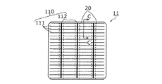
太陽電池モジュール1の主たる構成要素である太陽電池素子11の構造について説明する。
本実施の形態に係る太陽電池モジュール1の構造について、要部特徴を中心に説明する。
本実施の形態に係る中間部材40は、第1ポリオレフィン系材料及び第2ポリオレフィン系材料よりも極性の高い、または、吸水性の高い高分子材料を主成分とする部材である。さらに、平面視において太陽電池素子11が配置されていない領域であって、表面充填部材60と裏面充填部材70との界面に配置されている。つまり、中間部材40は、これらの材料及び配置を満たすような構造であればよい。ここで、本実施の形態に係る中間部材は、上記のように吸水性及び吸湿性に優れているだけでなく、光拡散及び光反射機能を有することが望ましい。以下、本実施の形態に係る中間部材が、さらに光拡散及び光反射機能を有する構成を、変形例1〜7に示す。
なお、太陽電池モジュールの製造工程では、隣接する太陽電池素子11の間に中間部材を配置する工程の後、表面保護部材80、裏面保護部材90、表面充填部材60及び裏面充填部材70が所定箇所に形成される。このため、中間部材の配置工程では、中間部材を、隣接する太陽電池素子11の間に固定しておく必要がある。以下の変形例6及び7では、中間部材を隣接する太陽電池素子11の間に固定するための構成について説明する。
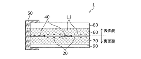
本実施の形態に係る太陽電池モジュール1は、複数の太陽電池素子11と、複数の太陽電池素子11の表面側に配置された、第1ポリオレフィン系材料を含む表面充填部材60と、複数の太陽電池素子11の裏面側に配置された、第2ポリオレフィン系材料を含む裏面充填部材70と、表面充填部材60と裏面充填部材70との界面に配置され、平面視において太陽電池素子11が配置された領域以外に配置され、第1ポリオレフィン系材料及び第2ポリオレフィン系材料よりも極性の高い、または、第1ポリオレフィン系材料及び第2ポリオレフィン系材料よりも吸水性の高い高分子材料を含む中間部材40と、複数の太陽電池素子11とで表面充填部材60を挟むように配置された表面保護部材80と、複数の太陽電池素子11とで裏面充填部材70を挟むように配置された裏面保護部材90とを備える。
以上、本発明に係る太陽電池モジュールについて、上記実施の形態に基づいて説明したが、本発明は、上記の実施の形態に限定されるものではない。
11 太陽電池素子
40、40A、40B、40C、40D、40E、45、46 中間部材
41 第1高分子層
42 第2高分子層
43 金属層
60 表面充填部材
70 裏面充填部材
80 表面保護部材
90 裏面保護部材
Claims (6)
- 複数の太陽電池素子と、
前記複数の太陽電池素子の受光面側である表面側に配置された、第1ポリオレフィン系材料を含む表面充填部材と、
前記複数の太陽電池素子の裏面側に配置された、第2ポリオレフィン系材料を含む裏面充填部材と、
前記表面充填部材と前記裏面充填部材との間に配置され、前記表面充填部材及び前記裏面充填部材と接し、前記第1ポリオレフィン系材料及び前記第2ポリオレフィン系材料よりも極性の高い、または、前記第1ポリオレフィン系材料及び前記第2ポリオレフィン系材料よりも吸水性の高い高分子材料を含む中間部材と、
前記複数の太陽電池素子とで前記表面充填部材を挟むように配置された表面保護部材と、
前記複数の太陽電池素子とで前記裏面充填部材を挟むように配置された裏面保護部材とを備え、
前記中間部材は、
前記高分子材料を主成分とする第1高分子層と、
前記高分子材料よりも硬質である高分子材料を主成分とする第2高分子層と、を備え、
前記第2高分子層は前記第1高分子層よりも表面側に配置され、前記第1高分子層は前記第2高分子層よりも裏面側に配置され、
前記第1高分子層は、前記裏面充填部材と接しており、
前記中間部材の表面には、複数の凹凸が形成されている
太陽電池モジュール。 - 前記中間部材は、さらに、
前記第2高分子層の表面に形成された金属層を備える
請求項1に記載の太陽電池モジュール。 - 前記第2高分子層及び前記金属層には、複数の凹凸が形成されている
請求項2に記載の太陽電池モジュール。 - 前記第1高分子層の上に、前記第2高分子層が形成されている
請求項3に記載の太陽電池モジュール。 - 前記第1高分子層の主成分である前記高分子材料は、エチレンビニルアセテートであり、
前記第2高分子層の主成分である前記高分子材料は、ポリエチレンテレフタレートである
請求項1〜4のいずれか1項に記載の太陽電池モジュール。 - 前記中間部材は、さらに、前記第2高分子層の表面に形成された金属層を備え、
前記中間部材は、前記複数の太陽電池素子のうちの隣り合う2つの太陽電池素子の間に配置され、
前記2つの太陽電池素子は、前記中間部材を介して導通していない、
請求項1に記載の太陽電池モジュール。
Applications Claiming Priority (3)
| Application Number | Priority Date | Filing Date | Title |
|---|---|---|---|
| JP2014125779 | 2014-06-18 | ||
| JP2014125779 | 2014-06-18 | ||
| PCT/JP2015/002955 WO2015194146A1 (ja) | 2014-06-18 | 2015-06-12 | 太陽電池モジュール |
Publications (2)
| Publication Number | Publication Date |
|---|---|
| JPWO2015194146A1 JPWO2015194146A1 (ja) | 2017-04-20 |
| JP6590261B2 true JP6590261B2 (ja) | 2019-10-16 |
Family
ID=54935153
Family Applications (1)
| Application Number | Title | Priority Date | Filing Date |
|---|---|---|---|
| JP2016529033A Active JP6590261B2 (ja) | 2014-06-18 | 2015-06-12 | 太陽電池モジュール |
Country Status (4)
| Country | Link |
|---|---|
| US (2) | US10074759B2 (ja) |
| EP (1) | EP3159936A4 (ja) |
| JP (1) | JP6590261B2 (ja) |
| WO (1) | WO2015194146A1 (ja) |
Families Citing this family (3)
| Publication number | Priority date | Publication date | Assignee | Title |
|---|---|---|---|---|
| JP1618129S (ja) * | 2018-03-28 | 2018-11-19 | ||
| US10134923B1 (en) * | 2018-04-27 | 2018-11-20 | Global Solar Energy, Inc. | Photovoltaic devices including bi-layer pixels having reflective and/or antireflective properties |
| JP6924887B1 (ja) * | 2020-11-02 | 2021-08-25 | ジョジアン ジンコ ソーラー カンパニー リミテッド | 光起電力モジュール |
Family Cites Families (14)
| Publication number | Priority date | Publication date | Assignee | Title |
|---|---|---|---|---|
| US5994641A (en) * | 1998-04-24 | 1999-11-30 | Ase Americas, Inc. | Solar module having reflector between cells |
| US20030000568A1 (en) * | 2001-06-15 | 2003-01-02 | Ase Americas, Inc. | Encapsulated photovoltaic modules and method of manufacturing same |
| JP4974472B2 (ja) * | 2005-03-30 | 2012-07-11 | 三洋電機株式会社 | 太陽電池モジュール及びこれを備えた太陽電池装置 |
| JP4662151B2 (ja) | 2005-11-29 | 2011-03-30 | 大日本印刷株式会社 | 太陽電池モジュール用充填材、およびそれを用いた太陽電池モジュール、ならびに太陽電池モジュール用充填材の製造方法 |
| JP2011159711A (ja) | 2010-01-29 | 2011-08-18 | Sanyo Electric Co Ltd | 太陽電池モジュール |
| JP2012089663A (ja) * | 2010-10-19 | 2012-05-10 | Fujifilm Corp | 太陽電池モジュール、および、太陽電池モジュールの製造方法 |
| JP2012119434A (ja) | 2010-11-30 | 2012-06-21 | Sanyo Electric Co Ltd | 太陽電池モジュール及びその製造方法 |
| JP2013012589A (ja) * | 2011-06-29 | 2013-01-17 | Sanyo Electric Co Ltd | 太陽電池モジュール |
| JP2013125778A (ja) * | 2011-12-13 | 2013-06-24 | Fuji Electric Co Ltd | 太陽電池モジュールおよびその製造方法 |
| CN102664210B (zh) * | 2012-05-14 | 2015-05-06 | 友达光电股份有限公司 | 太阳能模块与其制造方法 |
| JP6069316B2 (ja) * | 2012-06-14 | 2017-02-01 | 株式会社クラレ | 多層構造体およびそれを用いたデバイス、ならびにそれらの製造方法 |
| KR101890324B1 (ko) * | 2012-06-22 | 2018-09-28 | 엘지전자 주식회사 | 태양 전지 모듈 및 이에 적용되는 리본 결합체 |
| CN102800730A (zh) * | 2012-07-09 | 2012-11-28 | 友达光电股份有限公司 | 光伏装置 |
| WO2014033802A1 (ja) * | 2012-08-27 | 2014-03-06 | 三洋電機株式会社 | 太陽電池モジュール |
-
2015
- 2015-06-12 WO PCT/JP2015/002955 patent/WO2015194146A1/ja active Application Filing
- 2015-06-12 JP JP2016529033A patent/JP6590261B2/ja active Active
- 2015-06-12 EP EP15810466.1A patent/EP3159936A4/en not_active Withdrawn
-
2016
- 2016-12-15 US US15/381,040 patent/US10074759B2/en active Active
-
2018
- 2018-07-25 US US16/045,693 patent/US20180331243A1/en not_active Abandoned
Also Published As
| Publication number | Publication date |
|---|---|
| US20170098725A1 (en) | 2017-04-06 |
| US10074759B2 (en) | 2018-09-11 |
| EP3159936A4 (en) | 2017-06-14 |
| JPWO2015194146A1 (ja) | 2017-04-20 |
| WO2015194146A1 (ja) | 2015-12-23 |
| EP3159936A1 (en) | 2017-04-26 |
| US20180331243A1 (en) | 2018-11-15 |
Similar Documents
| Publication | Publication Date | Title |
|---|---|---|
| JP6526774B2 (ja) | 太陽電池モジュール | |
| JP6183717B2 (ja) | 太陽電池モジュール | |
| JP6624418B2 (ja) | 太陽電池モジュール | |
| JP5874011B2 (ja) | 太陽電池及び太陽電池モジュール | |
| JP6709977B2 (ja) | 太陽電池モジュール | |
| EP3067937B1 (en) | Solar cell module | |
| US20170373210A1 (en) | Solar cell module | |
| US20180331243A1 (en) | Solar cell module | |
| US20170365727A1 (en) | Solar cell module | |
| JPWO2020054130A1 (ja) | 太陽電池モジュール | |
| JP2006278695A (ja) | 太陽電池モジュール | |
| TWM502963U (zh) | 太陽能電池模組 | |
| KR101616131B1 (ko) | 태양전지 모듈 | |
| US10784384B2 (en) | Solar cell module | |
| JP6025123B2 (ja) | 太陽電池モジュール | |
| JP2017050514A (ja) | 太陽電池モジュール | |
| WO2015194147A1 (ja) | 太陽電池モジュール | |
| JP6771200B2 (ja) | 太陽電池モジュール | |
| JP6722910B2 (ja) | 太陽電池モジュール及び太陽電池モジュールの製造方法 | |
| JP2016192436A (ja) | 太陽電池モジュール | |
| JP5906422B2 (ja) | 太陽電池及び太陽電池モジュール | |
| JP6528196B2 (ja) | 太陽電池モジュール | |
| JP6495650B2 (ja) | 太陽電池モジュールおよびこれを用いた太陽電池アレイ | |
| JP7483382B2 (ja) | 太陽電池モジュール | |
| JP6731660B2 (ja) | 太陽電池モジュール |
Legal Events
| Date | Code | Title | Description |
|---|---|---|---|
| A621 | Written request for application examination |
Free format text: JAPANESE INTERMEDIATE CODE: A621 Effective date: 20180209 |
|
| A131 | Notification of reasons for refusal |
Free format text: JAPANESE INTERMEDIATE CODE: A131 Effective date: 20190212 |
|
| A521 | Written amendment |
Free format text: JAPANESE INTERMEDIATE CODE: A523 Effective date: 20190410 |
|
| A131 | Notification of reasons for refusal |
Free format text: JAPANESE INTERMEDIATE CODE: A131 Effective date: 20190604 |
|
| A521 | Written amendment |
Free format text: JAPANESE INTERMEDIATE CODE: A523 Effective date: 20190802 |
|
| TRDD | Decision of grant or rejection written | ||
| A01 | Written decision to grant a patent or to grant a registration (utility model) |
Free format text: JAPANESE INTERMEDIATE CODE: A01 Effective date: 20190903 |
|
| A61 | First payment of annual fees (during grant procedure) |
Free format text: JAPANESE INTERMEDIATE CODE: A61 Effective date: 20190905 |
|
| R151 | Written notification of patent or utility model registration |
Ref document number: 6590261 Country of ref document: JP Free format text: JAPANESE INTERMEDIATE CODE: R151 |