WO2015190488A1 - シフトレジスタ回路、及びそれを備えた表示装置 - Google Patents
シフトレジスタ回路、及びそれを備えた表示装置 Download PDFInfo
- Publication number
- WO2015190488A1 WO2015190488A1 PCT/JP2015/066621 JP2015066621W WO2015190488A1 WO 2015190488 A1 WO2015190488 A1 WO 2015190488A1 JP 2015066621 W JP2015066621 W JP 2015066621W WO 2015190488 A1 WO2015190488 A1 WO 2015190488A1
- Authority
- WO
- WIPO (PCT)
- Prior art keywords
- tft
- gate
- gate line
- potential
- voltage
- Prior art date
- Legal status (The legal status is an assumption and is not a legal conclusion. Google has not performed a legal analysis and makes no representation as to the accuracy of the status listed.)
- Ceased
Links
Images



















Classifications
-
- G—PHYSICS
- G09—EDUCATION; CRYPTOGRAPHY; DISPLAY; ADVERTISING; SEALS
- G09G—ARRANGEMENTS OR CIRCUITS FOR CONTROL OF INDICATING DEVICES USING STATIC MEANS TO PRESENT VARIABLE INFORMATION
- G09G3/00—Control arrangements or circuits, of interest only in connection with visual indicators other than cathode-ray tubes
- G09G3/20—Control arrangements or circuits, of interest only in connection with visual indicators other than cathode-ray tubes for presentation of an assembly of a number of characters, e.g. a page, by composing the assembly by combination of individual elements arranged in a matrix no fixed position being assigned to or needed to be assigned to the individual characters or partial characters
- G09G3/34—Control arrangements or circuits, of interest only in connection with visual indicators other than cathode-ray tubes for presentation of an assembly of a number of characters, e.g. a page, by composing the assembly by combination of individual elements arranged in a matrix no fixed position being assigned to or needed to be assigned to the individual characters or partial characters by control of light from an independent source
- G09G3/36—Control arrangements or circuits, of interest only in connection with visual indicators other than cathode-ray tubes for presentation of an assembly of a number of characters, e.g. a page, by composing the assembly by combination of individual elements arranged in a matrix no fixed position being assigned to or needed to be assigned to the individual characters or partial characters by control of light from an independent source using liquid crystals
- G09G3/3611—Control of matrices with row and column drivers
- G09G3/3648—Control of matrices with row and column drivers using an active matrix
-
- G—PHYSICS
- G09—EDUCATION; CRYPTOGRAPHY; DISPLAY; ADVERTISING; SEALS
- G09G—ARRANGEMENTS OR CIRCUITS FOR CONTROL OF INDICATING DEVICES USING STATIC MEANS TO PRESENT VARIABLE INFORMATION
- G09G3/00—Control arrangements or circuits, of interest only in connection with visual indicators other than cathode-ray tubes
- G09G3/20—Control arrangements or circuits, of interest only in connection with visual indicators other than cathode-ray tubes for presentation of an assembly of a number of characters, e.g. a page, by composing the assembly by combination of individual elements arranged in a matrix no fixed position being assigned to or needed to be assigned to the individual characters or partial characters
- G09G3/34—Control arrangements or circuits, of interest only in connection with visual indicators other than cathode-ray tubes for presentation of an assembly of a number of characters, e.g. a page, by composing the assembly by combination of individual elements arranged in a matrix no fixed position being assigned to or needed to be assigned to the individual characters or partial characters by control of light from an independent source
- G09G3/36—Control arrangements or circuits, of interest only in connection with visual indicators other than cathode-ray tubes for presentation of an assembly of a number of characters, e.g. a page, by composing the assembly by combination of individual elements arranged in a matrix no fixed position being assigned to or needed to be assigned to the individual characters or partial characters by control of light from an independent source using liquid crystals
- G09G3/3611—Control of matrices with row and column drivers
- G09G3/3674—Details of drivers for scan electrodes
- G09G3/3677—Details of drivers for scan electrodes suitable for active matrices only
-
- G—PHYSICS
- G11—INFORMATION STORAGE
- G11C—STATIC STORES
- G11C19/00—Digital stores in which the information is moved stepwise, e.g. shift registers
- G11C19/28—Digital stores in which the information is moved stepwise, e.g. shift registers using semiconductor elements
-
- G—PHYSICS
- G09—EDUCATION; CRYPTOGRAPHY; DISPLAY; ADVERTISING; SEALS
- G09G—ARRANGEMENTS OR CIRCUITS FOR CONTROL OF INDICATING DEVICES USING STATIC MEANS TO PRESENT VARIABLE INFORMATION
- G09G2300/00—Aspects of the constitution of display devices
- G09G2300/04—Structural and physical details of display devices
- G09G2300/0404—Matrix technologies
- G09G2300/0408—Integration of the drivers onto the display substrate
-
- G—PHYSICS
- G09—EDUCATION; CRYPTOGRAPHY; DISPLAY; ADVERTISING; SEALS
- G09G—ARRANGEMENTS OR CIRCUITS FOR CONTROL OF INDICATING DEVICES USING STATIC MEANS TO PRESENT VARIABLE INFORMATION
- G09G2300/00—Aspects of the constitution of display devices
- G09G2300/04—Structural and physical details of display devices
- G09G2300/0421—Structural details of the set of electrodes
- G09G2300/0426—Layout of electrodes and connections
-
- G—PHYSICS
- G09—EDUCATION; CRYPTOGRAPHY; DISPLAY; ADVERTISING; SEALS
- G09G—ARRANGEMENTS OR CIRCUITS FOR CONTROL OF INDICATING DEVICES USING STATIC MEANS TO PRESENT VARIABLE INFORMATION
- G09G2310/00—Command of the display device
- G09G2310/02—Addressing, scanning or driving the display screen or processing steps related thereto
- G09G2310/0264—Details of driving circuits
- G09G2310/0286—Details of a shift registers arranged for use in a driving circuit
-
- G—PHYSICS
- G09—EDUCATION; CRYPTOGRAPHY; DISPLAY; ADVERTISING; SEALS
- G09G—ARRANGEMENTS OR CIRCUITS FOR CONTROL OF INDICATING DEVICES USING STATIC MEANS TO PRESENT VARIABLE INFORMATION
- G09G2310/00—Command of the display device
- G09G2310/08—Details of timing specific for flat panels, other than clock recovery
Definitions
- 6C is a schematic diagram illustrating an arrangement example of elements of the drive circuit illustrated in FIG. 5.
- 6D is a schematic diagram illustrating an arrangement example of elements of the drive circuit illustrated in FIG. 5.
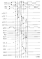
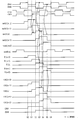
- FIG. 7 is a timing chart when the driving circuit according to the first embodiment drives the gate line.
- FIG. 8 is a diagram illustrating an example of an equivalent circuit of a conventional drive circuit.
- FIG. 9 is a diagram for explaining a change in the potential of netA in the conventional drive circuit and the drive circuit in the first embodiment.
- FIG. 10 is a diagram illustrating an example of an equivalent circuit of the drive circuit in the application example of the first embodiment.
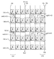
- FIG. 11 is a schematic diagram showing an arrangement example of elements of the drive circuit shown in FIG. FIG.
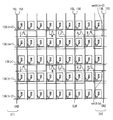
- FIG. 28C is a schematic diagram illustrating an arrangement example of some elements of the drive circuit illustrated in FIG. 27.
- FIG. 28D is a schematic diagram illustrating an arrangement example of some elements of the drive circuit illustrated in FIG. 27.
- FIG. 28E is a schematic diagram illustrating an arrangement example of some elements of the drive circuit illustrated in FIG. 27.
- FIG. 29 is a timing chart when the drive circuit in the first modification drives the gate line.
- FIG. 30 is a timing chart when the driving circuit according to the second modification drives a part of the gate lines.
- the first configuration has a plurality of drive circuits connected to each gate line.
- Each of the drive circuits includes an output unit, a precharge unit, a boosting unit, a gate voltage charging unit, a gate line discharging unit, and an internal wiring.
- the output unit includes a switching element that outputs a selection voltage to one gate line.
- the precharge unit includes a switching element that outputs a control voltage for operating the switching element of the output unit.
- the boosting unit includes a capacitor and a switching element that charges the capacitor, and boosts the gate voltage of the switching element of the output unit via the capacitor.
- the gate voltage discharge unit includes a switching element that lowers the gate voltage of the switching element of the output unit during a non-selection period of one gate line.
- the control voltage output from the precharge unit is input to the gate terminal of the switching element of the output unit via the internal wiring.
- a booster is connected to the internal wiring, and the gate voltage of the switching element of the output unit is boosted via the internal wiring. That is, the potential of the internal wiring is boosted above the control voltage output from the precharge unit.
- At least one of the switching elements of the precharge portion, the gate voltage discharge portion, and the gate line discharge portion is turned on by the potential of the internal wiring in another drive circuit.
- the gate voltage can be charged to the potential of another gate line without depending on the threshold voltage of the switching element of the precharge unit.
- the switching element of the gate voltage discharging unit has a gate terminal connected to the internal wiring in the other drive circuit, and a source terminal connected to the internal wiring.
- the drain terminal may be supplied with a control signal that switches between a potential corresponding to the selected state and a potential corresponding to the non-selected state at regular intervals.
- the control signal that switches between the potential corresponding to the selected state of the gate line and the potential corresponding to the non-selected state is applied to the drain terminal of the switching element of the gate voltage discharging unit at a certain period. Therefore, the gate voltage can be lowered at an appropriate timing in the non-selection period of the gate line.
- the control signal that switches between the potential corresponding to the selected state of the gate line and the potential corresponding to the non-selected state is supplied to the source terminal of the switching element of the gate line discharge unit at a certain period. Since it is input, the gate line can be brought into a non-selected state at an appropriate timing in the non-selected period of the gate line.
- the switching element in the output unit has a source terminal connected to the one gate line, and a drain terminal having a potential corresponding to the selected state.
- a direct-current voltage signal may be supplied.
- the DC voltage signal indicating the potential corresponding to the selected state of the gate line is input to the drain terminal of the switching element of the output unit. Therefore, it is possible to reduce the load and power consumption for operating the output unit, compared to the case where a control signal that repeats the potential corresponding to the selected state and the potential corresponding to the non-selected state is input at regular intervals. .
- any gate line can be switched to the selected state.
- the active matrix substrate is provided with a plurality of source lines intersecting with each of the plurality of gate lines, and the driving circuit includes the plurality of source lines. It may be provided in a display region defined by a gate line and the plurality of source lines.
- FIG. 1 is a schematic diagram showing a schematic configuration of the liquid crystal display device according to the present embodiment.
- the liquid crystal display device 1 includes a display panel 2, a source driver 3, a display control circuit 4, and a power source 5.
- the display panel 2 includes an active matrix substrate 20a, a counter substrate 20b, and a liquid crystal layer (not shown) sandwiched between these substrates.
- a pair of polarizing plates is provided so as to sandwich the active matrix substrate 20a and the counter substrate 20b.
- a black matrix, three color filters of red (R), green (G), and blue (B) and a common electrode (all not shown) are formed on the counter substrate 20b.
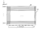
- FIG. 2 is a schematic diagram showing a schematic configuration of the active matrix substrate 20a.
- M M: natural number
- gate lines 13G (1) to 13G (M) are formed substantially in parallel at regular intervals from one end to the other end in the X-axis direction.
- gate lines 13G A plurality of source lines 15S are formed on the active matrix substrate 20a so as to intersect with the gate lines 13G.
- a region surrounded by the gate line 13G and the source line 15S forms one pixel, and each pixel corresponds to one of the colors of the color filter.
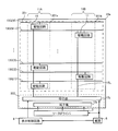
- FIG. 3 is a schematic diagram showing a schematic configuration of each part connected to the active matrix substrate 20a and the active matrix substrate 20a.
- the source line 15S is not shown for convenience.
- the active matrix substrate 20a is provided with gate drivers 11A and 11B in the areas 201a and 201b of the display area 201, respectively.
- the gate driver 11A includes a plurality of drive circuits 11 provided for the odd-numbered gate lines 13G of the gate lines 13G (1), 13G (3),... 13G (M) and connected via the wiring 15L.
- the gate driver 11B is provided for the gate lines 13G in even rows of the gate lines 13G (2), 13G (4),... 13G (M ⁇ 1), and is connected to the plurality of drives connected via the wiring 15L.
- a circuit 11 is included.
- a terminal portion 12g is provided in the frame region 202 on the side where the source driver 3 is provided.
- the terminal portion 12g is connected to the display control circuit 4 and the power source 5.
- the terminal unit 12g receives signals such as a control signal and a power supply voltage signal output from the display control circuit 4 and the power supply 5. Signals such as a control signal and a power supply voltage signal input to the terminal portion 12g are supplied to each drive circuit 11 via the wiring 15L.
- the drive circuit 11 outputs a voltage signal indicating one of the selected state and the non-selected state to the connected gate line 13G.
- the state where the gate line 13G is selected is referred to as driving of the gate line 13G.
- a terminal portion 12s for connecting the source driver 3 and the source line 15S is provided in the frame region 202 of the active matrix substrate 20a.
- the source driver 3 outputs a data signal to each source line 15S (see FIG. 2) in accordance with a control signal input from the display control circuit 4.
- the display control circuit 4 has, as a control signal, a signal that repeats an H level (VDD) and an L level (VSS) every two horizontal periods (hereinafter referred to as a clock signal), and the same potential as the H level of the clock signal.
- a signal (hereinafter referred to as a reset signal) is supplied to the terminal portion 12g.
- FIG. 4 is a diagram illustrating the waveform of the clock signal.
- four-phase clock signals CKA, CKC, CKB, and CKD whose phases are shifted by 1 ⁇ 4 period, are supplied to the terminal unit 12g as clock signals.
- a four-phase clock signal is used.
- the H-level (VDD) and the L-level (VSS) are repeated every one horizontal scanning period, and the two-phase clock is shifted by 1/2 cycle.
- a plurality of clock signals having different phases such as signals may be used.
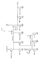
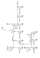
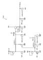
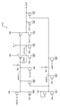
- the drive circuit 11 (n) includes thin film transistors (TFT: Thin Film Transistor) (hereinafter referred to as TFT-A to TFT-L) indicated by alphabets A to L and a capacitor Cbst as switching elements.
- TFT Thin Film Transistor
- the source terminal of TFT-B, the drain terminals of TFT-A, TFT-C, and TFT-K, the gate terminal of TFT-F, and one electrode of capacitor Cbst are connected.
- the wiring is referred to as netA.
- An internal wiring in which the source terminal of TFT-G, the drain terminals of TFT-H, TFT-I, and TFT-J and the gate terminal of TFT-C are connected is referred to as netB.
- the netA and the netB have parasitic capacitances Cpa and Cpb between the source line 15S (see FIG. 2) and other elements provided in the pixel, respectively. Have.
- TFT-A The drain terminal of TFT-A is connected to netA, the reset signal CLR is supplied to the gate terminal, and the power supply voltage signal VSS is supplied to the source terminal.
- the TFT-A lowers netA (n) to L level (VSS) in accordance with the potential of the reset signal CLR.
- the gate terminal of the TFT-B in the drive circuit 11 (n) is connected to the gate line 13G (n-2) driven two horizontal scanning periods before the drive timing of the gate line 13G (n).
- the potential of netA (n-2) of the drive circuit 11 (n-2) provided is input.
- the TFT-B outputs the potential of the set signal S to the netA (n) according to the potential of the netA (n-2), and charges (precharges) the netA (n).
- the TFT-K has a gate terminal connected to the gate line 13G (n + 2), a drain terminal connected to netA (n), and a power supply voltage signal VSS is supplied to the source terminal.
- the TFT-K lowers netA (n) to the L level (VSS) in accordance with the potential of the gate line 13G (n + 2).
- the TFT-F has a gate terminal connected to netA (n), a source terminal connected to the gate line 13G (n), and a clock signal CKA supplied to the drain terminal.
- the TFT-F outputs the potential of the clock signal CKA to the gate line 13G (n) according to the potential of netA (n), charges the capacitor Cbst, and switches the gate line 13G (n) to the selected state.
- the TFT-F drives a gate line with a relatively heavy load, it is necessary to increase the channel width.
- the TFT-F is represented by one TFT, but the TFT-F is configured by connecting a plurality of TFTs. A specific configuration example of the TFT-F will be described later.
- the capacitor Cbst has one electrode connected to the netA (n) and the other electrode connected to the gate line 13G (n).
- the capacitor Cbst boosts the potential of netA (n) in accordance with the potential of the clock signal CKA output from the TFT-F.
- the TFT-E has a drain terminal connected to the gate line 13G (n), a reset signal CLR supplied to the gate terminal, and a power supply voltage signal VSS supplied to the source terminal.
- the TFT-E lowers the potential of the gate line 13G (n) to the L level (VSS) in accordance with the potential of the reset signal CLR.
- the TFT-D has a drain terminal connected to the gate line 13G (n), a clock signal CKB supplied to the gate terminal, and a power supply voltage signal VSS supplied to the source terminal.
- the TFT-D lowers the potential of the gate line 13G (n) to the L level (VSS) in accordance with the potential of the clock signal CKB.
- the TFT-L has a drain terminal connected to the gate line 13G (n), a gate terminal connected to the gate line 13G (n + 2), and a power supply voltage signal VSS is supplied to the source terminal.
- the TFT-L lowers the potential of the gate line 13G (n) to the L level (VSS) in accordance with the potential of the gate line 13G (n + 2).
- a gate terminal and a drain terminal are connected, a clock signal CKD is supplied to the gate terminal and the drain terminal, and a source terminal is connected to netB (n).
- the TFT-G outputs a potential of (H level potential of the clock signal CKD ⁇ threshold voltage) to the netB (n) in accordance with the potential of the clock signal CKD.
- TFT-H has a drain terminal connected to netB (n), a gate terminal supplied with a clock signal CKC, and a source terminal supplied with a power supply voltage signal VSS.
- the TFT-H pulls netB (n) to the L level (VSS) potential in accordance with the potential of the clock signal CKC.
- TFT-I has a drain terminal connected to netB (n), a gate terminal supplied with a reset signal CLR, and a source terminal supplied with a power supply voltage signal VSS.
- the TFT-I lowers netB (n) to the L level (VSS) potential in accordance with the potential of the reset signal CLR.
- the TFT-F functions as an output unit that outputs a selection voltage corresponding to the selected state to the gate line 13G (n).
- the TFT-B functions as a precharge unit that outputs a control voltage for operating the TFT-F to the netA (n) and charges the netA (n).
- the TFT-F and the capacitor Cbst function as a boosting unit that boosts the gate voltage of the TFT-F by boosting the potential of netA (n).
- TFT-A, TFT-K, and TFT-C function as a gate voltage discharge unit that lowers the potential of netA (n).
- the TFT-E, TFT-D, and TFT-L function as a gate line discharge unit that outputs a non-selection voltage to the gate line 13G.
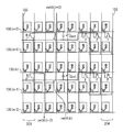
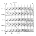
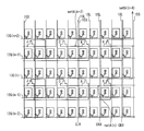
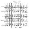
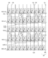
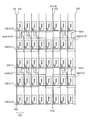
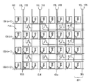
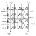
- FIGS. 6A to 6D are schematic diagrams illustrating an arrangement example of the drive circuit 11 (n) and the drive circuit 11 (n + 2).
- 6A to 6D for the sake of convenience, only alphabets A to L are shown, and the notation of “TFT-” is omitted. It corresponds. 6A to 6D are assumed to be continuous in the columns 201 to 204.
- each element constituting the drive circuit 11 (n) is arranged between the gate lines 13G (n ⁇ 2) to 13G (n).
- Each element constituting the drive circuit 11 (n + 2) is disposed between the gate lines 13G (n) to 13G (n + 2).
- the drive circuit 11 (n) is connected to the gate line 13G (n ⁇ 1), the gate line 13G (n), and the gate line 13G (n + 2), and the drive circuit 11 (n + 2) is connected to the gate line 13G (n + 1),
- the gate line 13G (n + 2) and the gate line 13G (n + 4) are connected.
- the TFT-A, TFT-K, TFT-D, and TFT-L are connected via a wiring 15L that supplies a power supply voltage signal VSS.
- the TFT-H and TFT-G of the drive circuit 11 are connected via wirings 15L for supplying clock signals CKC and CKD, respectively.
- the wiring 15L for supplying the power supply voltage signal VSS includes TFT-E, TFT-I, TFT-H, TFT-G, TFT-J, TFT-C, TFT-A, and TFT.
- the wiring is provided from the terminal portion 12g (see FIG. 3) so as to be substantially parallel to the source line 15S, and is routed to the pixel in which these TFTs are arranged.
- the wiring 15L for supplying the power supply voltage signal VSS is connected to the source line 15S from the terminal portion 12g (see FIG. 3) in another column different from the column in which the TFT-D and TFT-L are arranged. Are wired so as to be substantially parallel to each other, and are routed to pixels where these TFTs are arranged.
- the gate terminal of the TFT-H in the driving circuit 11 (n) is connected to the wiring 15L for supplying the clock signal CKC, and the gate terminal of the TFT-H in the driving circuit 11 (n + 2) is connected to the clock signal CKD. Is connected to the wiring 15L.
- the gate terminal of the TFT-G in the driving circuit 11 (n) is connected to the wiring 15L that supplies the clock signal CKD, and the gate terminal of the TFT-G in the driving circuit 11 (n + 2) is the wiring that supplies the clock signal CKC. It is connected to 15L.
- the TFT-F is configured by connecting three TFTs in parallel.
- the number of TFTs to be connected is not limited to this, and one or more TFTs may be connected.
- other TFTs and capacitors Cbst other than TFT-F may be configured by connecting a plurality of TFTs and capacitors in parallel as necessary.
- the drain terminals of the three TFT-Fs in the drive circuit 11 (n) are connected to the wiring 15L to which the clock signal CKA is supplied.
- the drain terminals of the three TFTs in the drive circuit 11 (n + 2) are connected to the wiring 15L to which the clock signal CKB is supplied.
- the wiring 15L for supplying the clock signals CKA and CKB to each TFT-F is substantially parallel to the source line 15S from the terminal portion 12g (see FIG. 3) in a column different from the column in which the TFT-F is arranged. To the pixel where each TFT-F is arranged.
- each drive circuit 11 in the gate drivers 11A and 11B is supplied with a clock signal having a phase opposite to that of the clock signal supplied to the adjacent drive circuit 11 in the gate driver. Further, the clock signals supplied to the drive circuit 11 that drives the adjacent gate line 13G are out of phase with each other by a quarter period.
- the clock signal CKA is input to the drain terminal of the TFT-F in the drive circuit 11 (n)
- the clock signal is applied to the drain terminal of the TFT-F in the drive circuit 11 (n-2) and the drive circuit 11 (n + 2).
- a signal CKB is input.
- the clock signal CKD is input to the drain terminal of the TFT-F in the driver circuit 11 (n ⁇ 1)
- the clock signal CKC is input to the drain terminal of the TFT-F in the driver circuit 11 (n + 1).
- FIG. 7 is a timing chart when the drive circuit 11 (n) drives the gate line 13G (n).
- the clock signals CKA, CKB, CKC, and CKD supplied from the display control circuit 4 are input to the drive circuit 11 (n).
- a reset signal CLR that is at a H (High) level for a certain period every vertical scanning period is input from the display control circuit 4 to each drive circuit 11.
- the reset signal CLR is input, the potentials of the netA (n), netB (n), and the gate line 13G in the driving circuit 11 (n) transition to the L (Low) level.
- the gate line 13G (n ⁇ 1) is switched to the selected state, and the set signal S is applied to the drain terminal of the TFT-B of the drive circuit 11 (n) as the set signal S.
- An H level potential is input.
- the potential of netA (n-2) is input to the gate terminal of the TFT-B.
- the potential of netA (n-2) is at the H level before time t1, and the TFT-B is in the on state at time t1.
- the TFT-B is turned on until time t2 when the potential of netA (n-2) transitions to the L level, and during time t1 to t2, netA (n) is at the H level of the gate line 13G (n-1). Is precharged to the potential (VDD).
- the gate terminal of TFT-F is inputted with the H level potential of netA (n) and is turned on.
- the TFT-D is turned on, and the L level potential (VSS) is input to the gate line 13G (n). Is done.
- the potential of the clock signal CKD is at the H level
- the potential of the clock signal CKC is at the L level.
- the TFT-G is turned on and the TFT-H is turned off.
- the H-level potential of the gate line 13G (n ⁇ 1) is input as the set signal S to the gate terminal of the TFT-J, and the TFT-J is turned on. Therefore, netB (n) is maintained at the L level potential, and the TFT-C is turned off.
- the potential of the clock signal CKA becomes H level, and the H level potential of the clock signal CKA is input to the gate line 13G (n) via the TFT-F.
- the capacitor Cbst connected between the netA (n) and the gate line 13G (n) causes the netA (n) to become higher than the H level potential of the clock signal CKA. Is charged to a high potential. That is, netA (n) is charged to a potential higher than (precharge voltage VDD + threshold voltage Vth of TFT-F).
- the drive circuit 11 (n + 1) that drives the gate line 13G (n + 1) operates in the same manner as the drive circuit 11 (n) using the gate line 13G (n) as the set signal S, and the gate line 13G (n + 1) ,
- the selected state is switched at time t3.
- the drive circuit 11 (n + 2) that drives the gate line 13G (n + 2) operates in the same manner as the drive circuit 11 (n) using the gate line 13G (n + 1) as the set signal S, and the gate line 13G (n + 2)
- the state is switched to the selected state at time t4.
- the potential of the clock signal CKB changes to H level, and the TFT-D is turned on.
- the TFT-K and the TFT-L are also turned on.
- an L-level potential is input to the gate line 13G (n) via the TFT-D and TFT-L, and the gate line 13G (n) is switched to a non-selected state.
- an L-level potential is input to netA (n) via TFT-K.
- the potential of the clock signal CKC is at the H level, and the TFT-H is kept on, so that the potential of netB (n) is maintained at the L level.
- netB (n) is for maintaining the potential of netA (n) at the L level via TFT-C.
- the drive circuit 11 (n) is configured so that the TFT-C is turned on in accordance with the potential of the clock signal CKD during the non-selection period of the gate line 13G (n).
- the TFT-F has a parasitic capacitance with the wiring 15L that supplies the clock signal CKA. Therefore, during the period in which netA (n) is held at the L level potential, noise synchronized with the clock signal CKA is input to netA (n) through the parasitic capacitance. In order to avoid this noise, the potential of netB (n) is changed to H level at the same timing as the clock signal CKD so that the TFT-C is turned on at the timing when the potential of the clock signal CKA becomes H level. Yes.
- FIG. 8 shows an equivalent circuit of a conventional driving circuit 100 (n) using a diode-connected TFT-B.
- the drive circuit 100 (n) shown in FIG. 8 has the same configuration as the drive circuit 11 (n) except that the potential of the gate line 13G (n-2) is input to the gate terminal and drain terminal of the TFT-B. is there.
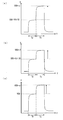
- FIG. 9A shows the netA (n) in the precharge period Tp of netA (n) and the selection period Ts of the gate line 13G (n) when the drive circuit 100 (n) is arranged outside the display region.
- FIG. 9B shows the netA (n) in the precharge period Tp of netA (n) and the selection period Ts of the gate line 13G (n) when the driving circuit 100 (n) is arranged in the display area. It is a figure showing the electric potential change of n).
- the TFT is applied from the H level potential (VDD) of the gate line 13G (n ⁇ 2) in the precharge period Tp.
- a potential (VDD ⁇ Vth (B)) that is smaller than the ⁇ B threshold voltage (Vth (B)) is precharged to netA (n).
- the H-level potential of the clock signal CKA is input to the gate line 13G (n) through the TFT-F, and the potential of the netA (n) is higher than the precharge voltage by the capacitor Cbst ( VDD + ⁇ ).
- the driver circuit 100 (n) when the driver circuit 100 (n) is provided in the display region, the driver circuit 100 (n) has a parasitic capacitance with another element such as the source line 15S provided in the display region, and netA (n ) Is larger than that provided outside the display area.
- the efficiency of increasing the potential of netA (n) via the capacitor Cbst is reduced, and as shown in FIG. 9B, the potential of netA (n) in the selection period Ts (VDD + ⁇ ( ⁇ ⁇ )) Is smaller than the case where the drive circuit 100 (n) is arranged outside the display area.
- the gate voltage of the TFT-F is lowered, the drive circuit cannot be stably operated, and the operation margin of the gate driver is lowered.
- the potential of netA (n-2) is input to the gate terminal of TFT-B, and the potential of gate line 13G (n-1) is input to the drain terminal as a set signal. .
- the precharge voltage of netA (n) in the precharge period Tp does not decrease by the threshold voltage of the TFT-B, and the H of the gate line 13G (n) This is the level potential (VDD).
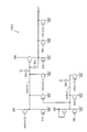
- FIG. 10 is a diagram illustrating an equivalent circuit of the drive circuit 110 in this application example.
- the drive circuit 110 (n) for driving the gate line 13G (n) is similar to the drive circuit 11 (n) except that the clock signal CKD is input to the drain terminal of the TFT-B. Have the same configuration.
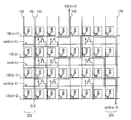
- FIG. 11 is a schematic diagram showing an example of TFT-B connection between the drive circuit 110 (n) in the display region and the drive circuit 110 (n + 2) that drives the gate line 13G (n + 2).
- the notation of “TFT-” is omitted for the sake of convenience, but the TFT indicated by the alphabet in FIG. 11 corresponds to the TFT having the same alphabet in FIG.
- the drain terminal of the TFT-B in the driving circuit 110 (n) is connected to the wiring 15L to which the clock signal CKD is supplied.
- the drain terminal of the TFT-B in the driving circuit 110 (n + 2) is connected to a wiring 15L to which a clock signal CKC having a phase opposite to that of the clock signal CKD is supplied.
- FIG. 12 is a timing chart when the driving circuit 110 (n) drives the gate line 13G (n). Hereinafter, operations different from those of the first embodiment will be described.
- the potential of the clock signal CKD becomes H level, and at this time, the TFT-B is in an on state. Therefore, the potential of the H level (VDD) of the clock signal CKD is transferred to the netA (n) via the TFT-B. Is precharged. Note that the clock signal CKD changes to the H level every two horizontal scanning periods, but the TFT-B is in the off state except during the period in which the potential of the netA (n-2) is at the H level. After t2, the H level potential of the clock signal CKD is not input to netA (n) via the TFT-B.
- the gate line 13G has a relatively large parasitic capacitance, and the output waveform of the gate line 13G tends to be dull. Therefore, as in the first embodiment, when the potential of the gate line 13G (n ⁇ 1) is input to the drain terminal of the TFT-B, the output waveform of the gate line 13G (n ⁇ 1) is affected by blunting. The ability to precharge netA (n) via TFT-B is reduced. In addition, as the TFTs in the drive circuit 110 deteriorate, the output waveform of the gate line 13G becomes increasingly dull. As a result, the ability to precharge netA (n) is further reduced, and the operation of the drive circuit becomes unstable. In the application example of the first embodiment, since a clock signal is input to the drain terminal of the TFT-B, netA can be appropriately precharged regardless of the degree of blunting of the output waveform of the gate line 13G.
- FIG. 13 is a diagram showing an equivalent circuit of the drive circuit 111 in the present embodiment.
- the precharge TFT-B of netA (n) is diode-connected in the driving circuit 111 (n) that drives the gate line 13G (n) in the driving circuit 111 (n) that drives the gate line 13G (n) in the driving circuit 111 (n) that drives the gate line 13G (n) in the driving circuit 111 (n) that drives the gate line 13G (n) is diode-connected.
- the potential of the gate line 13G (n-2) is input to the gate terminal and the drain terminal of the TFT-B.
- the potential of netA (n + 2) in the drive circuit 111 (n + 2) that drives the gate line 13G (n + 2) is input to the gate terminal of the TFT-K, and the potential of the clock signal CKA is input to the drain terminal.
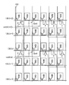
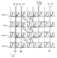
- FIGS. 14A and 14B are schematic diagrams illustrating a connection example of the driver circuit 111 (n) and the TFT-K and TFT-B of the driver circuit 111 (n + 2) in the display region. 14 and 14B, the notation of “TFT-” is omitted for the sake of convenience, but the TFTs indicated by alphabets in FIGS. 14A and 14B correspond to the TFTs denoted by the same alphabets in FIG.
- the gate terminal of the TFT-K in the drive circuit 111 (n) is connected to netA (n + 2), and the gate terminal of the TFT-K in the drive circuit 111 (n + 2) is connected to netA (n + 4). It is connected.
- the drain terminal of the TFT-K in the driving circuit 111 (n) is connected to the wiring 15L that supplies the clock signal CKA, and the drain terminal of the TFT-K in the driving circuit 111 (n + 2) is the wiring 15L that supplies the clock signal CKB. It is connected to the.
- the gate terminal and the drain terminal of the TFT-B in the driving circuit 111 (n) are connected to the gate line 13G (n-2), and the TFT-B in the driving circuit 111 (n + 2) is connected.
- the gate terminal and the drain terminal are connected to the gate line 13G (n).
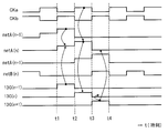
- FIG. 15 is a timing chart when the drive circuit 111 (n) drives the gate line 13G (n). Hereinafter, operations different from those of the first embodiment will be described.
- the gate line 13G (n-2) is in a selected state, and the gate line 13G (n-2) of the TFT-B in the driver circuit 111 (n) is connected to the gate terminal and the drain terminal.
- An H level potential is input.
- the TFT-B is turned on, and a potential that is smaller than the H-level potential of the gate line 13G (n-2) by the threshold voltage of the TFT-B is precharged to the netA (n) via the TFT-B. Is done.
- the H level potential of the clock signal CKA is input to the gate line 13G (n) via the TFT-F.
- the potential of netA (n) is raised to a potential higher than the H level of the clock signal CKA via the capacitor Cbst, and the potential of netA (n) is input to the gate terminal of the TFT-F, and the gate line 13G (n ) Is inputted with the H level potential of the clock signal CKA.
- the TFT-J in the driver circuit 111 (n) is turned on during the period from time t1 to time t3 when the potential of the gate line 13G (n-1) becomes H level, and the TFT-H has the potential of the clock signal CKC. It is turned on during the period from time t3 to time t5 when it becomes H level. Thus, from time t1 to time t5, netB (n) is maintained at the L level potential.
- netA (n + 1) starts precharging at time t1
- the gate line 13G (n + 1) is switched to the selected state at time t3.
- the netA (n + 2) starts to be precharged at time t2, and the gate line 13G (n + 2) is switched to the selected state at time t4.
- netA (n + 2) is connected to the gate terminal of TFT-K that lowers netA (n) to L level.
- the netA in the drive circuit 111 is pushed up to a potential higher than the selection voltage via the capacitor Cbst during the selection period of the gate line 13G. Therefore, the gate voltage of the TFT-K is improved, the value of the current flowing from the drain terminal to the source terminal of the TFT-K is increased, and the driving force of the TFT-K is improved.
- the driving circuit 111 can be stably operated.
- FIG. 16 is a diagram illustrating an equivalent circuit of the drive circuit 112 in the present embodiment.
- the driving circuit 112 (n) for driving the gate line 13G (n) the TFT-K for lowering the potential of netA (n) is connected to the gate line 13G (n + 2) at the gate terminal.
- NetA (n) is connected to the drain terminal, and the power supply voltage signal VSS is input to the source terminal.
- the TFT-L that outputs a non-selection voltage to the gate line 13G (n) has a gate terminal connected to the netA (n + 2) in the drive circuit 112 (n + 2), a drain terminal to which the clock signal CKA is input, A gate line 13G (n) is connected to the terminal.
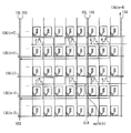
- FIGS. 17A and 17B are schematic diagrams illustrating a connection example of the driver circuit 112 (n) and the TFT-K and TFT-L of the driver circuit 112 (n + 2) in the display region.
- the notation of “TFT-” is omitted, but the TFTs indicated by alphabets in FIGS. 17A and 17B correspond to the TFTs denoted by the same alphabets in FIG.
- the gate terminal of the TFT-K in the drive circuit 112 (n) is connected to the gate line 13G (n + 2), and the gate terminal of the TFT-K in the drive circuit 112 (n + 2) is connected to the gate line 13G. Connected to (n + 4).
- the source terminal of the TFT-K in the drive circuit 112 (n) and the drive circuit 112 (n + 2) is connected to the wiring 15L that supplies the power supply voltage signal VSS.
- TFT-D pulls down netC (n) to the L level potential in accordance with the potential of the clock signal CKB input to the gate terminal.
- the drive circuit 115 since the drive circuit 115 is operated using a two-phase clock signal, the number of wirings 15L for supplying the clock signal can be reduced and the clock signal is supplied compared to the first embodiment. Power consumption can be reduced.
Landscapes
- Engineering & Computer Science (AREA)
- Chemical & Material Sciences (AREA)
- Crystallography & Structural Chemistry (AREA)
- Physics & Mathematics (AREA)
- Computer Hardware Design (AREA)
- General Physics & Mathematics (AREA)
- Theoretical Computer Science (AREA)
- Control Of Indicators Other Than Cathode Ray Tubes (AREA)
- Liquid Crystal Display Device Control (AREA)
- Liquid Crystal (AREA)
- Shift Register Type Memory (AREA)
Abstract
Description
(液晶表示装置の構成)
図1は、本実施形態に係る液晶表示装置の概略構成を示した模式図である。液晶表示装置1は、表示パネル2、ソースドライバ3、表示制御回路4、及び電源5を有する。表示パネル2は、アクティブマトリクス基板20aと、対向基板20bと、これら基板に挟持された液晶層(図示略)とを有する。図1において図示を省略しているが、アクティブマトリクス基板20aと対向基板20bとを挟むように、一対の偏光板が設けられている。対向基板20bには、ブラックマトリクスと、赤(R)、緑(G)、青(B)の3色のカラーフィルタと、共通電極(いずれも図示略)が形成されている。
図2は、アクティブマトリクス基板20aの概略構成を示す模式図である。アクティブマトリクス基板20aにおいて、X軸方向の一端から他端までM(M:自然数)本のゲート線13G(1)~13G(M)が一定の間隔で略平行に形成されている。以下、ゲート線を区別しないときは、ゲート線13Gと称する。アクティブマトリクス基板20aには、各ゲート線13Gと交差するように複数のソース線15Sが形成されている。ゲート線13Gとソース線15Sとで囲まれる領域が1つの画素を形成し、各画素は、カラーフィルタのいずれかの色に対応している。
次に、本実施形態における駆動回路11の構成について説明する。図5は、ゲート線13G(n)を駆動する駆動回路11(以下、駆動回路11(n))の等価回路の一例を示す図である。
次に、本実施形態における駆動回路11の配置例について説明する。図6A~図6Dは、駆動回路11(n)及び駆動回路11(n+2)の配置例を示す模式図である。なお、図6A~図6Dでは、便宜上、アルファベットA~Lのみ記載し、”TFT-”の表記を省略しているが、A~Lは、図5に示したTFT-A~TFT-Lに対応している。また、図6A~6Dに示す各表示領域は、列201~204において連続しているものとする。
次に、駆動回路11の動作について説明する。図7は、駆動回路11(n)がゲート線13G(n)を駆動する際のタイミングチャートである。
上述した第1実施形態では、駆動回路11(n)のTFT-Bに入力されるセット信号Sとしてゲート線13G(n-1)の電位を入力する例について説明した。本応用例では、TFT-Bに入力されるセット信号Sとしてクロック信号を入力する例について説明する。以下の説明において、第1実施形態と異なる構成について説明する。
図10は、本応用例における駆動回路110の等価回路を例示した図である。図10に示すように、ゲート線13G(n)を駆動する駆動回路110(n)は、TFT-Bのドレイン端子に、クロック信号CKDが入力される点を除き、駆動回路11(n)と同じ構成を有する。
図11は、表示領域における駆動回路110(n)と、ゲート線13G(n+2)を駆動する駆動回路110(n+2)のTFT-Bの接続例を示す模式図である。なお、図11では、便宜上、”TFT-”の表記を省略しているが、図11においてアルファベットで示すTFTは、図10における同じアルファベットが付されたTFTと対応している。図11に示すように、駆動回路110(n)におけるTFT-Bのドレイン端子は、クロック信号CKDが供給される配線15Lに接続されている。また、駆動回路110(n+2)におけるTFT-Bのドレイン端子は、クロック信号CKDと逆位相のクロック信号CKCが供給される配線15Lに接続されている。
図12は、駆動回路110(n)がゲート線13G(n)を駆動する際のタイミングチャートである。以下、第1実施形態と異なる動作について説明する。
上述の第1実施形態とその応用例では、netAのプリチャージ電圧の低下を抑制し、ゲートドライバの動作マージンを向上させる例を説明した。ゲートドライバの動作マージンの低下の要因として、ゲート線を非選択期間に切り替える際のnetAの電位の引き下げが不十分であることが挙げられる。特に、表示領域内にゲートドライバを配置する場合には、表示領域内に配置されたソース線15Sや配線15L等の素子との間に生じる寄生容量の影響を受け、netAを確実にLレベルに引き下げることができないことがある。本実施形態では、ゲートドライバの動作マージンを向上させるべく、ゲート線を非選択状態に遷移させる際にnetAの電位の引き下げをより確実に行う例を説明する。以下、第1実施形態と異なる構成について説明する。
図13は、本実施形態における駆動回路111の等価回路を示す図である。図13に示すように、ゲート線13G(n)を駆動する駆動回路111(n)は、netA(n)のプリチャージ用のTFT-Bは、ダイオード接続されている。TFT-Bのゲート端子とドレイン端子には、ゲート線13G(n-2)の電位が入力される。また、TFT-Kのゲート端子には、ゲート線13G(n+2)を駆動する駆動回路111(n+2)におけるnetA(n+2)の電位が入力され、ドレイン端子には、クロック信号CKAの電位が入力される。
図14A及び14Bは、表示領域における駆動回路111(n)と、駆動回路111(n+2)のTFT-K、及びTFT-Bの接続例を示す模式図である。なお、図14及び14Bでは、便宜上、”TFT-”の表記を省略しているが、図14A及び14Bにおいてアルファベットで示すTFTは、図13における同じアルファベットが付されたTFTと対応している。
図15は、駆動回路111(n)がゲート線13G(n)を駆動する際のタイミングチャートである。以下、第1実施形態と異なる動作について説明する。
上述した第2実施形態では、ゲートドライバの動作マージンを向上させるべく、ゲート電圧放電部として機能するTFT-Kのゲート端子に、他の駆動回路のnetAを接続し、TFT-Kの駆動力を向上させる例を説明した。本実施形態では、ゲート線の非選択期間の遷移時におけるゲート線の放電を強化し、ゲートドライバの動作マージンの向上を図る。以下、第2実施形態と異なる構成について説明する。
図16は、本実施形態における駆動回路112の等価回路を例示した図である。図16に示すように、ゲート線13G(n)を駆動する駆動回路112(n)において、netA(n)の電位を引き下げるためのTFT-Kは、ゲート端子にゲート線13G(n+2)が接続され、ドレイン端子にnetA(n)が接続され、ソース端子に電源電圧信号VSSが入力されている。また、ゲート線13G(n)に非選択電圧を出力するTFT-Lは、ゲート端子に、駆動回路112(n+2)におけるnetA(n+2)が接続され、ドレイン端子にクロック信号CKAが入力され、ソース端子にゲート線13G(n)が接続されている。
図17A及び17Bは、表示領域における駆動回路112(n)と、駆動回路112(n+2)のTFT-K、及びTFT-Lの接続例を示す模式図である。なお、図17A及び17Bでは、便宜上、”TFT-”の表記を省略しているが、図17A及び17Bにおいてアルファベットで示すTFTは、図16における同じアルファベットが付されたTFTと対応している。
次に、駆動回路112(n)の動作について説明する。図18は、駆動回路112(n)がゲート線13G(n)を駆動する際のタイミングチャートである。以下、第2実施形態と異なる駆動回路112(n)の動作について、図18及び図16を用いて説明する。
上述した第1実施形態から第3実施形態では、出力部として機能するTFTのドレイン端子と、ゲート線放電部として機能するTFTのドレイン端子にクロック信号を入力し、クロック信号を用いてゲート線を充電する例を説明した。本実施形態では、Hレベル(VDD)の直流電圧信号を用いて充電する例について説明する。
図19は、本実施形態における駆動回路113の等価回路を例示した図である。図19に示すように、ゲート線13G(n)を駆動する駆動回路113(n)は、以下の点において、第1実施形態の応用例の駆動回路と異なっている。
次に、本実施形態における駆動回路の表示領域における配置例について説明する。図20A~20Fは、表示領域における駆動回路113(n)と駆動回路113(n+2)の配置例を示す模式図である。図20A~20Fは、列211~215において連続しているものとする。また、各図では、便宜上、”TFT”の表記を省略しているが、A~N、Pが付されたTFTは、図19に示すTFT-A~TFT-N、及びTFT-Pを示している。以下、主に、第1実施形態の応用例と異なる構成の配置について説明する。
次に、駆動回路113(n)の動作について説明する。図21は、駆動回路113(n)がゲート線13G(n)を駆動する際のタイミングチャートである。以下、第1実施形態の応用例と異なる動作について、図21及び図19を用いて説明する。
上述した第4実施形態では、M本のゲート線13Gを順次駆動する例について説明したが、本実施形態では、任意のゲート線13Gを駆動させる例について説明する。
図22は、本実施形態における駆動回路114の等価回路を例示した図である。図22に示すゲート線13G(n)を駆動する駆動回路114(n)は、第4実施形態における駆動回路113(n)と以下の点において異なる。
図23A~23Dは、駆動回路114(n)と、ゲート線13G(n+2)を駆動する駆動回路114(n+2)におけるTFT-J、TFT-K、TFT-Pを含む一部の素子が配置された表示領域を示す模式図である。図23A~23Dは、列221~223において連続しているものとする。また、図23A~23Dにおいて、便宜上、”TFT-”の表記を省略しているが、各図においてアルファベットを付したTFTは、図22において同じアルファベットが付されたTFTに対応している。
次に、本実施形態における駆動回路の動作について説明する。図24は、1フレームにおいて、一部のゲート線13Gを駆動する際のタイミングチャートである。以下、第4実施形態と異なる動作について説明する。
。
以上、本発明の実施の形態を説明したが、上述した実施の形態は本発明を実施するための例示に過ぎない。よって、本発明は上述した実施の形態に限定されることなく、その趣旨を逸脱しない範囲内で上述した実施の形態を適宜変形、又は組み合わせて実施することが可能である。以下、本発明の変形例について説明する。
図25は、本変形例におけるアクティブマトリクス基板の概略構成を示す模式図である。なお、図25において、ソース線15S(図2参照)の図示は省略されている。図25に示すように、本変形例では、アクティブマトリクス基板20aにおける表示領域201において、ゲート線13Gごとに一の駆動回路115が設けられたゲートドライバ115Aを有する。各駆動回路115は、配線15Lを介して接続されている。
図27は、駆動回路115の等価回路を例示した図である。図27に示すように、ゲート線13G(n)を駆動する駆動回路115(n)は、第1実施形態における駆動回路11を構成するTFT-F、TFT-G、TFT-Hに入力されるクロック信号と、TFT-Bのゲート端子に入力されるnetAの電位と、TFT-K、及びTFT-Lのゲート端子に入力されるゲート線13Gの電位とが異なる点を除き、駆動回路11と同じ構成である。つまり、本実施形態では、TFT-Fのドレイン端子には、クロック信号CKaが入力される。TFT-Gのゲート端子及びドレイン端子には、クロック信号CKbが入力される。TFT-Hのゲート端子には、クロック信号CKaが入力される。TFT-Bのゲート端子には、ゲート線13G(n-1)を駆動する駆動回路115(n-1)におけるnetA(n-1)の電位が入力される。TFT-K、及びTFT-Lのゲート端子には、ゲート線13G(n+1)の電位が入力される。
次に、表示領域における駆動回路115の配置例について説明する。図28A~28Eは、ゲート線13G(n-1)~ゲート線13G(n+1)を各々駆動する駆動回路115(n-1)、駆動回路115(n)、駆動回路115(n+1)、が配置された画素を示す模式図である。図28A~28Eでは、便宜上、”TFT-”の表記は省略しているが、図28A~28EのA~Lで示す各TFTは、図27に示すTFT-A~TFT-Lに対応する。また、図28A~28Eは、列231~234において連続しているものとする。
次に、本変形例における駆動回路115の動作について説明する。図29は、駆動回路115によるゲート線13Gの駆動タイミングを示すタイミングチャートである。
Claims (9)
- アクティブマトリクス基板に設けられた複数のゲート線の各々を、選択状態、又は非選択状態に切り替えるシフトレジスタ回路であって、
前記シフトレジスタ回路は、個々のゲート線に接続され、当該ゲート線を選択状態又は非選択状態に切り替える駆動回路を複数有し、
前記駆動回路の各々は、
一のゲート線に接続され、前記一のゲート線を選択状態に切り替える選択電圧を出力するスイッチング素子を含む出力部と、
前記出力部におけるスイッチング素子を動作させるための制御電圧を出力するスイッチング素子を含むプリチャージ部と、
キャパシタと、前記キャパシタを充電するスイッチング素子とを有し、前記キャパシタを介して、前記出力部におけるスイッチング素子のゲート電圧を昇圧する昇圧部と、
前記一のゲート線を非選択状態に切り替える非選択期間に、前記ゲート電圧を引き下げるスイッチング素子を含むゲート電圧放電部と、
前記一のゲート線の非選択期間に、前記一のゲート線に非選択電圧を出力するスイッチング素子を含むゲート線放電部と、
前記出力部におけるスイッチング素子のゲート端子、前記プリチャージ部、前記ゲート電圧放電部、前記昇圧部が接続されている内部配線と、を備え、
前記プリチャージ部、前記ゲート電圧放電部、及び前記ゲート線放電部におけるスイッチング素子のうちの少なくとも一のスイッチング素子のゲート端子は、他の駆動回路における前記内部配線に接続されている、シフトレジスタ回路。 - 前記プリチャージ部のスイッチング素子は、ゲート端子が、前記他の駆動回路における前記内部配線に接続され、ソース端子は、前記内部配線に接続され、ドレイン端子は、他のゲート線に接続されている、請求項1に記載のシフトレジスタ回路。
- 前記プリチャージ部のスイッチング素子は、ゲート端子が、前記他の駆動回路における前記内部配線に接続され、ソース端子は、前記内部配線に接続され、ドレイン端子は、一定周期ごとに、前記選択状態に対応する電位と前記非選択状態に対応する電位との間で切り替わる制御信号が供給される、請求項1に記載のシフトレジスタ回路。
- 前記ゲート電圧放電部のスイッチング素子は、ゲート端子が、前記他の駆動回路における前記内部配線に接続され、ソース端子は、前記内部配線に接続され、ドレイン端子は、一定周期ごとに、前記選択状態に対応する電位と前記非選択状態に対応する電位との間で切り替わる制御信号が供給される、請求項1に記載のシフトレジスタ回路。
- 前記ゲート線放電部のスイッチング素子は、ゲート端子が、前記他の駆動回路における前記内部配線に接続され、ソース端子は、前記内部配線に接続され、ドレイン端子は、一定周期ごとに、前記選択状態に対応する電位と前記非選択状態に対応する電位との間で切り替わる制御信号が供給される、請求項1に記載のシフトレジスタ回路。
- 前記出力部におけるスイッチング素子は、ソース端子が前記一のゲート線に接続され、ドレイン端子は、前記選択状態に対応する電位を示す直流電圧信号が供給される、請求項1から5のいずれか一項に記載のシフトレジスタ回路。
- 前記出力部のスイッチング素子は、ソース端子が前記一のゲート線に接続され、ドレイン端子は、前記選択状態、及び前記非選択状態の一方に対応する電位を示す指示信号が供給される、請求項1から5のいずれか一項に記載のシフトレジスタ回路。
- 前記アクティブマトリクス基板に、前記複数のゲート線の各々と交差する複数のソース線が設けられ、
前記駆動回路は、前記複数のゲート線と前記複数のソース線とで規定される表示領域に設けられている、請求項1から7のいずれか一項に記載のシフトレジスタ回路。 - 請求項1から8のいずれか一項に記載のシフトレジスタ回路を備えるアクティブマトリクス基板と、
カラーフィルタを有する対向基板と、
前記アクティブマトリクス基板と前記対向基板との間に挟持された液晶層と、
を有する表示装置。
Priority Applications (3)
| Application Number | Priority Date | Filing Date | Title |
|---|---|---|---|
| CN201580031373.8A CN106463178A (zh) | 2014-06-13 | 2015-06-09 | 移位寄存器电路和具备其的显示装置 |
| US15/318,043 US20180108309A1 (en) | 2014-06-13 | 2015-06-09 | Shift register circuit, and display device including same |
| JP2016527828A JPWO2015190488A1 (ja) | 2014-06-13 | 2015-06-09 | シフトレジスタ回路、及びそれを備えた表示装置 |
Applications Claiming Priority (2)
| Application Number | Priority Date | Filing Date | Title |
|---|---|---|---|
| JP2014-122391 | 2014-06-13 | ||
| JP2014122391 | 2014-06-13 |
Publications (1)
| Publication Number | Publication Date |
|---|---|
| WO2015190488A1 true WO2015190488A1 (ja) | 2015-12-17 |
Family
ID=54833578
Family Applications (1)
| Application Number | Title | Priority Date | Filing Date |
|---|---|---|---|
| PCT/JP2015/066621 Ceased WO2015190488A1 (ja) | 2014-06-13 | 2015-06-09 | シフトレジスタ回路、及びそれを備えた表示装置 |
Country Status (4)
| Country | Link |
|---|---|
| US (1) | US20180108309A1 (ja) |
| JP (1) | JPWO2015190488A1 (ja) |
| CN (1) | CN106463178A (ja) |
| WO (1) | WO2015190488A1 (ja) |
Cited By (1)
| Publication number | Priority date | Publication date | Assignee | Title |
|---|---|---|---|---|
| CN107331295A (zh) * | 2016-04-29 | 2017-11-07 | 群创光电股份有限公司 | 显示器面板 |
Families Citing this family (6)
| Publication number | Priority date | Publication date | Assignee | Title |
|---|---|---|---|---|
| JP2019191396A (ja) * | 2018-04-26 | 2019-10-31 | シャープ株式会社 | 表示装置 |
| CN112967691B (zh) * | 2021-02-04 | 2022-10-18 | 业成科技(成都)有限公司 | 闸极驱动电路、闸极驱动装置与拼接式显示器 |
| KR102832919B1 (ko) * | 2021-03-16 | 2025-07-11 | 삼성디스플레이 주식회사 | 표시 장치와 그를 포함하는 타일형 표시 장치 |
| KR102813548B1 (ko) | 2021-03-16 | 2025-05-28 | 삼성디스플레이 주식회사 | 표시 장치 및 이를 포함하는 타일형 표시 장치 |
| CN114882848B (zh) * | 2022-05-13 | 2024-07-05 | 重庆惠科金渝光电科技有限公司 | 栅极驱动电路及显示装置 |
| CN115294915B (zh) * | 2022-08-29 | 2023-07-18 | 惠科股份有限公司 | 栅极驱动电路和显示装置 |
Citations (6)
| Publication number | Priority date | Publication date | Assignee | Title |
|---|---|---|---|---|
| JPH10197851A (ja) * | 1997-01-07 | 1998-07-31 | Toshiba Corp | 液晶表示装置 |
| US20080016139A1 (en) * | 2006-07-12 | 2008-01-17 | Wintek Corporation | Shift register with each stage controlled by a specific voltage of the next stage and the stage after thereof |
| US20110142192A1 (en) * | 2009-12-11 | 2011-06-16 | Chih-Ying Lin | Shift register circuit |
| US20120155604A1 (en) * | 2010-12-16 | 2012-06-21 | Yu-Chung Yang | Shift register circuit |
| US20120170707A1 (en) * | 2010-12-29 | 2012-07-05 | Kuo-Hua Hsu | Switch device and shift register circuit using the same |
| WO2014142183A1 (ja) * | 2013-03-15 | 2014-09-18 | シャープ株式会社 | アクティブマトリクス基板、アクティブマトリクス基板の製造方法、及び表示パネル |
Family Cites Families (6)
| Publication number | Priority date | Publication date | Assignee | Title |
|---|---|---|---|---|
| US7969400B2 (en) * | 2004-02-25 | 2011-06-28 | Hitachi Displays, Ltd. | Liquid crystal display device with decreased power consumption |
| TWI366814B (en) * | 2006-07-12 | 2012-06-21 | Wintek Corp | Shift register |
| TWI379310B (en) * | 2008-08-27 | 2012-12-11 | Au Optronics Corp | Shift register |
| US9299452B2 (en) * | 2012-08-09 | 2016-03-29 | Innocom Technology (Shenzhen) Co., Ltd. | Shift registers, display panels, display devices, and electronic devices |
| WO2014208123A1 (ja) * | 2013-06-28 | 2014-12-31 | シャープ株式会社 | 単位シフトレジスタ回路、シフトレジスタ回路、単位シフトレジスタ回路の制御方法及び表示装置 |
| WO2015033838A1 (ja) * | 2013-09-04 | 2015-03-12 | シャープ株式会社 | アクティブマトリクス基板、表示パネル及びそれを備えた表示装置 |
-
2015
- 2015-06-09 WO PCT/JP2015/066621 patent/WO2015190488A1/ja not_active Ceased
- 2015-06-09 US US15/318,043 patent/US20180108309A1/en not_active Abandoned
- 2015-06-09 CN CN201580031373.8A patent/CN106463178A/zh not_active Withdrawn
- 2015-06-09 JP JP2016527828A patent/JPWO2015190488A1/ja active Pending
Patent Citations (6)
| Publication number | Priority date | Publication date | Assignee | Title |
|---|---|---|---|---|
| JPH10197851A (ja) * | 1997-01-07 | 1998-07-31 | Toshiba Corp | 液晶表示装置 |
| US20080016139A1 (en) * | 2006-07-12 | 2008-01-17 | Wintek Corporation | Shift register with each stage controlled by a specific voltage of the next stage and the stage after thereof |
| US20110142192A1 (en) * | 2009-12-11 | 2011-06-16 | Chih-Ying Lin | Shift register circuit |
| US20120155604A1 (en) * | 2010-12-16 | 2012-06-21 | Yu-Chung Yang | Shift register circuit |
| US20120170707A1 (en) * | 2010-12-29 | 2012-07-05 | Kuo-Hua Hsu | Switch device and shift register circuit using the same |
| WO2014142183A1 (ja) * | 2013-03-15 | 2014-09-18 | シャープ株式会社 | アクティブマトリクス基板、アクティブマトリクス基板の製造方法、及び表示パネル |
Cited By (1)
| Publication number | Priority date | Publication date | Assignee | Title |
|---|---|---|---|---|
| CN107331295A (zh) * | 2016-04-29 | 2017-11-07 | 群创光电股份有限公司 | 显示器面板 |
Also Published As
| Publication number | Publication date |
|---|---|
| US20180108309A1 (en) | 2018-04-19 |
| CN106463178A (zh) | 2017-02-22 |
| JPWO2015190488A1 (ja) | 2017-06-01 |
Similar Documents
| Publication | Publication Date | Title |
|---|---|---|
| JP6498327B2 (ja) | 電気光学装置 | |
| JP5079350B2 (ja) | シフトレジスタ回路 | |
| JP5128102B2 (ja) | シフトレジスタ回路およびそれを備える画像表示装置 | |
| JP4990034B2 (ja) | シフトレジスタ回路およびそれを備える画像表示装置 | |
| JP5436324B2 (ja) | シフトレジスタ回路 | |
| US10121429B2 (en) | Active matrix substrate, display panel, and display device including the same | |
| CN104137170B (zh) | 显示装置 | |
| WO2015190488A1 (ja) | シフトレジスタ回路、及びそれを備えた表示装置 | |
| KR102680560B1 (ko) | 게이트 구동 회로와 이를 이용한 표시장치 | |
| JP2008251094A (ja) | シフトレジスタ回路およびそれを備える画像表示装置 | |
| KR102268519B1 (ko) | 두얼 출력 gip 구조 | |
| WO2012063696A1 (ja) | 液晶表示装置 | |
| JPWO2015163305A1 (ja) | アクティブマトリクス基板、及びそれを備えた表示装置 | |
| WO2015163306A1 (ja) | アクティブマトリクス基板、及びそれを備えた表示装置 | |
| KR102309625B1 (ko) | 게이트 구동 회로, 게이트 구동 회로의 구동방법 및 이를 이용한 표시장치 | |
| KR101027827B1 (ko) | 쉬프트 레지스터 및 그 구동 방법 | |
| JP5631145B2 (ja) | ゲート信号線駆動回路及び表示装置 | |
| JP2011170300A (ja) | 表示装置制御回路 | |
| JP2007207411A (ja) | シフトレジスタ回路およびそれを備える画像表示装置 | |
| KR101297241B1 (ko) | 액정표시장치의 구동장치 | |
| JP5610778B2 (ja) | 走査線駆動回路 | |
| JP2024107550A (ja) | 走査信号線駆動回路および表示装置 | |
| JP5457251B2 (ja) | 電気光学装置 | |
| JP2007242129A (ja) | シフトレジスタ回路およびそれを備える画像表示装置 |
Legal Events
| Date | Code | Title | Description |
|---|---|---|---|
| 121 | Ep: the epo has been informed by wipo that ep was designated in this application |
Ref document number: 15806928 Country of ref document: EP Kind code of ref document: A1 |
|
| ENP | Entry into the national phase |
Ref document number: 2016527828 Country of ref document: JP Kind code of ref document: A |
|
| NENP | Non-entry into the national phase |
Ref country code: DE |
|
| WWE | Wipo information: entry into national phase |
Ref document number: 15318043 Country of ref document: US |
|
| 122 | Ep: pct application non-entry in european phase |
Ref document number: 15806928 Country of ref document: EP Kind code of ref document: A1 |