WO2015182541A1 - 積層偏光フィルムの欠陥検査方法、製造方法および製造装置 - Google Patents
積層偏光フィルムの欠陥検査方法、製造方法および製造装置 Download PDFInfo
- Publication number
- WO2015182541A1 WO2015182541A1 PCT/JP2015/064873 JP2015064873W WO2015182541A1 WO 2015182541 A1 WO2015182541 A1 WO 2015182541A1 JP 2015064873 W JP2015064873 W JP 2015064873W WO 2015182541 A1 WO2015182541 A1 WO 2015182541A1
- Authority
- WO
- WIPO (PCT)
- Prior art keywords
- light
- film
- inspection
- polarizing film
- surface side
- Prior art date
- Legal status (The legal status is an assumption and is not a legal conclusion. Google has not performed a legal analysis and makes no representation as to the accuracy of the status listed.)
- Ceased
Links
Images

Classifications
-
- G—PHYSICS
- G01—MEASURING; TESTING
- G01N—INVESTIGATING OR ANALYSING MATERIALS BY DETERMINING THEIR CHEMICAL OR PHYSICAL PROPERTIES
- G01N21/00—Investigating or analysing materials by the use of optical means, i.e. using sub-millimetre waves, infrared, visible or ultraviolet light
- G01N21/84—Systems specially adapted for particular applications
- G01N21/88—Investigating the presence of flaws or contamination
- G01N21/89—Investigating the presence of flaws or contamination in moving material, e.g. running paper or textiles
-
- G—PHYSICS
- G01—MEASURING; TESTING
- G01N—INVESTIGATING OR ANALYSING MATERIALS BY DETERMINING THEIR CHEMICAL OR PHYSICAL PROPERTIES
- G01N21/00—Investigating or analysing materials by the use of optical means, i.e. using sub-millimetre waves, infrared, visible or ultraviolet light
- G01N21/84—Systems specially adapted for particular applications
- G01N21/88—Investigating the presence of flaws or contamination
- G01N21/89—Investigating the presence of flaws or contamination in moving material, e.g. running paper or textiles
- G01N21/892—Investigating the presence of flaws or contamination in moving material, e.g. running paper or textiles characterised by the flaw, defect or object feature examined
-
- G—PHYSICS
- G01—MEASURING; TESTING
- G01N—INVESTIGATING OR ANALYSING MATERIALS BY DETERMINING THEIR CHEMICAL OR PHYSICAL PROPERTIES
- G01N21/00—Investigating or analysing materials by the use of optical means, i.e. using sub-millimetre waves, infrared, visible or ultraviolet light
- G01N21/84—Systems specially adapted for particular applications
- G01N21/88—Investigating the presence of flaws or contamination
- G01N21/89—Investigating the presence of flaws or contamination in moving material, e.g. running paper or textiles
- G01N21/892—Investigating the presence of flaws or contamination in moving material, e.g. running paper or textiles characterised by the flaw, defect or object feature examined
- G01N21/896—Optical defects in or on transparent materials, e.g. distortion, surface flaws in conveyed flat sheet or rod
-
- G—PHYSICS
- G02—OPTICS
- G02B—OPTICAL ELEMENTS, SYSTEMS OR APPARATUS
- G02B5/00—Optical elements other than lenses
- G02B5/30—Polarising elements
Definitions
- the present invention relates to a method, a manufacturing method, and a manufacturing apparatus for inspecting a defect of a laminated polarizing film.
- the polarizing film is widely used as an optical film used by being bonded to the surface of a liquid crystal cell in a liquid crystal display device such as a television.
- a polarizing film conventionally, for example, a polarizer protective film made of triacetyl cellulose (TAC) or the like is applied to a polarizer film obtained by adsorbing and orienting a dichroic dye on a polyvinyl alcohol (PVA) film.
- TAC triacetyl cellulose
- PVA polyvinyl alcohol
- the polarizing film is shipped as a laminated polarizing film in which a release film (separate film) is laminated on one surface via an adhesive layer, and a protective film is laminated on the other surface.
- An adhesive layer is for bonding on the surface of a liquid crystal cell.
- a release film is a film for protecting an adhesive layer until it bonds to a liquid crystal cell.
- the protective film is a film for preventing the polarizing film from being damaged.
- An object of the present invention is to provide a defect inspection method for a laminated polarizing film that can cope with many types of defects with a minimum necessary inspection method in the manufacturing process of the laminated polarizing film.
- the defect inspection method for the laminated polarizing film of the present invention includes a first laminating step for obtaining a polarizing film by laminating a polarizer protective film on a polarizer film, and one surface side of the polarizing film obtained by the first laminating step.
- the laminated film obtained through the production process of the laminated polarizing film including a second laminated step of laminating a release film via an adhesive layer and laminating a protective film on the other surface side to obtain a laminated polarizing film It is a method of inspecting for defects in a polarizing film,
- the polarizing film obtained by the first laminating step is irradiated with linearly polarized light having a vibrating surface parallel to the absorption axis of the polarizer film from one surface side, and transmitted light is detected.
- the first cross transmission inspection From one surface side, the vibration surface irradiates light containing linearly polarized light orthogonal to the absorption axis of the polarizer film, and detects transmitted light on an axis deviated from the optical axis of the irradiated light, From the other surface side, a first transmission scattering test for detecting transmitted light that irradiates irradiation light including linearly polarized light whose vibration plane is orthogonal to the absorption axis of the polarizer film, and Irradiating irradiation light from one surface side, and performing a first reflection / scattering inspection to detect a reflected light component directed in a direction deviating from the regular reflection direction of the irradiation light among the reflected light reflected, For the laminated polarizing film obtained by the second lamination step, From one surface side, the second cross transmission inspection that detects the transmitted light by irradiating the linearly polarized light whose vibration surface is parallel to the absorption axis of
- Irradiation light is emitted from one surface side, and the reflected light component of the reflected light that reflects away from the regular reflection direction of the irradiation light is detected, and the irradiation light is emitted from the other surface side and reflected.
- a second reflection / scattering inspection is performed to detect a reflected light component directed in a direction deviating from the regular reflection direction of the irradiated light.
- the present invention many types of defects can be dealt with in the manufacturing process of the laminated polarizing film with the minimum necessary inspection.
- the respective inspections can be performed in any order in the respective steps before and after the release film and the protective film are adhered, there is also an effect that the degree of freedom in the layout of the inspection steps is increased.
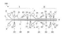
- FIG. 1 shows an automatic inspection apparatus 100 which is an embodiment of a defect inspection method according to the present invention.
- This automatic inspection apparatus 100 is obtained by laminating a polarizer protective film 2 via an adhesive layer on the upper and lower surfaces of a polarizer film 1 obtained by adsorbing and orienting a dichroic dye on a polyvinyl alcohol (PVA) film.
- PVA polyvinyl alcohol
- Defect inspection is performed on the second laminating step II to obtain the laminated polarizing film 6 by laminating 5.
- the polarizer protective film 2 is first laminated on at least one surface of the upper and lower surfaces of the polarizer film 1 to obtain the polarizing film 3.
- the polarizer film 1 absorbs linearly polarized light whose vibration surface is parallel to the absorption axis and does not transmit the transmitted light, and linearly polarized light whose vibration surface is orthogonal to the absorption axis remains as it is. It is an optical element to transmit.
- the light transmitted through the polarizer film 1 is linearly polarized light whose vibration surface is orthogonal to the absorption axis.
- the method of laminating the polarizer film 1 and the polarizer protective film 2 is not particularly limited, and for example, it may be laminated via an adhesive layer.
- the adhesive constituting the adhesive layer include an adhesive made of a vinyl alcohol polymer, an adhesive made of an epoxy resin, or at least vinyl such as boric acid, borax, glutaraldehyde, melamine, and oxalic acid.
- examples thereof include an adhesive composed of a water-soluble crosslinking agent of an alcohol polymer.
- this adhesive for example, there is also a so-called active energy ray curable adhesive that is cured by being irradiated with active energy rays such as ultraviolet rays and electron beams to adhere the polarizer film 1 and the polarizer protective film 2. Can be mentioned.
- the same polarizer protective film 2 may be used on both surfaces, or different polarizer protective films 2 may be used.
- a triacetyl cellulose film may be laminated as the polarizer protective film 2 on both sides of the polarizer film 1, a triacetyl cellulose film may be laminated only on one side, or a triacetyl cellulose film is laminated on one side. You may laminate
- the protective film 5 is stuck on the polarizer protective film 2, and the polarizer protective film 2 is attached.
- the pressure-sensitive adhesive layer and the release film 4 are preferably laminated in this order on the other surface side that is not laminated.
- the thickness of the polarizer film 1 is usually 1 to 50 ⁇ m, preferably 3 to 20 ⁇ m. When the thickness of the polarizer film 1 is 20 ⁇ m or less, the influence of deformation of the polarizer film due to defects such as foreign matters appears greatly, so the defect inspection method of the present invention is preferably applied.
- the thickness of the adhesive layer is usually 0.1 to 5 ⁇ m or less, preferably 1 ⁇ m or less.
- An appropriate transparent film can be used for the polarizer protective film 2 provided on at least one surface of the polarizer film 1.
- a film made of a polymer excellent in transparency, mechanical strength, thermal stability, moisture shielding property, etc. is preferably used.
- the polymer include acetate resins (for example, triacetyl cellulose (TAC)), polyester resins (for example, polyethylene terephthalate (PET)), acrylic resins, polyolefin resins (for example, polypropylene), and cyclic polyolefins. Based resins and the like.
- Such a film may be produced by any of the casting method, calendar method, and extrusion method, but an acetate-based resin such as triacetylcellulose is preferable from the viewpoint of polarization characteristics and durability, and the surface is particularly alkaline.
- a triacetyl cellulose film that has been saponified with, for example, is preferable.
- the polarizer protective film 2 is an acrylic resin, the acrylic resin easily breaks due to extreme deformation caused by foreign matter, and therefore the method of the present invention is preferably applied.
- the thickness of the polarizer protective film 2 is usually 5 to 100 ⁇ m, preferably 10 to 50 ⁇ m.
- the polarizer protective film 2 is laminated on the polarizer film 1 to obtain the polarizing film 3, and then the first cross transmission inspection 10, the first reflection / scattering inspection 20, and the first transmission. Three series of inspections including the scattering inspection 30 are performed.
- the polarizing film 3 flows in the direction of the second laminating process II by a conveying roller (not shown) while detecting a defect by the inspection shown below.
- the illumination 11 is disposed on either the upper or lower side of the polarizing film 3, the sensor 13 is disposed on the opposite side of the polarizing film 3, and the polarizing filter 12 is disposed between the illumination 11 and the polarizing film 3. .
- the polarizing film 3 is irradiated with linearly polarized light whose vibration surface is parallel to the absorption axis from the illumination 11 on one surface side through the polarizing filter 12, and transmitted light transmitted through the polarizing film 3.
- the defect which exists in the polarizing filter 12 side from the polarizer film 1 of the polarizing film 3 is detected.
- the polarizing filter 12 is an optical filter that directly transmits linearly polarized light whose vibration surface is parallel to the transmission axis, and does not pass orthogonally linearly polarized light.
- the polarizing filter 12 can be the same as the polarizing film 3 described above.
- the absorption axis of the polarizing filter 12 is orthogonal to the absorption axis of the polarizing film 3.
- Cross transmission means that a polarizing filter 12 is arranged so as to be crossed Nicol with the polarizing film 3, and the light from the illumination 11 is irradiated from one of the outer directions to the other surface. Point to.
- a fluorescent lamp, an LED, a metal halide lamp, or the like can be used, and a metal halide lamp is more preferable.
- a line sensor camera, an area sensor camera, or the like can be used as the above-mentioned illumination 11, for example, a fluorescent lamp, an LED, a metal halide lamp, or the like.
- the light irradiated by the first cross transmission inspection 10 and irradiated to the polarizing film through the polarizing filter 12 is linearly polarized light having a vibration plane orthogonal to the absorption axis of the polarizing filter 12 and is oscillated in parallel. It does not include a linearly polarized light component having a surface (the same applies to the second cross transmission test 60 described later).
- the visibility correction polarization degree (Py) indicating the ratio of the parallel polarization component and the orthogonal polarization component is obtained by the following calculation formula (1). This visibility correction polarization degree (Py) is usually 98% or more, ideally 100%.
- the optical characteristics of the polarizing film are measured with a spectrophotometer with an integrating sphere (manufactured by JASCO Corporation, V7100). MD transmittance and TD transmittance are obtained in the wavelength range of 380 nm to 780 nm, the degree of polarization at each wavelength is calculated based on Equation (1), and visibility correction is performed using the 2 degree field of view (C light source) of JIS Z 8701. To determine the visibility correction polarization degree (Py).
- MD transmittance is the transmittance when the direction of the vibration plane of the linearly polarized light emitted from the Glan-Thompson prism is parallel to the transmission axis of the polarizing plate sample.
- TD transmittance is the transmittance when the direction of the vibration plane of the linearly polarized light emitted from the Glan-Thompson prism is orthogonal to the transmission axis of the polarizing plate sample, and is expressed as “TD” in the equation (1).
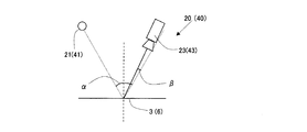
- the first reflection / scattering inspection 20 shown in the first lamination step I irradiates the polarizing film 3 with light from the obliquely arranged illumination 21 onto the polarizing film 3 and reflects the reflected light reflected on the polarizer film 1. Among them, the reflected light component traveling in the direction deviating from the regular reflection direction of the irradiated light is read by the sensor 23, and between the polarizer film 1 and the polarizer protective film 2 of the polarizing film 3 or on the polarizer protective film 2. The generated bubbles and irregularities on the polarizing film 3 are detected. At this time, as shown in FIG.
- the angle ⁇ between the incident light of the illumination 21 and the reflected light with respect to the polarizing film 3 is preferably 60 to 120 °.
- the sensor 23 tilts the polarizing film 3 with respect to a line formed by regular reflection of light irradiated from the illumination 21 onto the inspection portion on the polarizing film 3 with a tilt of ⁇ 20 to + 20 °, more preferably. Installed with inclinations of -6 to -2 ° and +2 to + 6 °.
- the sensor 23 senses and measures a light beam that is irradiated and reflected on the polarizing film 3.
- the defect detection means 20 may be installed on at least one of the upper and lower surfaces of the polarizing film 3, preferably installed on either the upper or lower surface, and more preferably a mold release provided with an adhesive layer in a subsequent step. It is installed on the side where the film 4 is laminated.
- the illumination 21 described above for example, a fluorescent lamp, an LED, a metal halide lamp, or the like can be used.
- the sensor 23 for example, a line sensor camera, an area sensor camera or the like can be used.
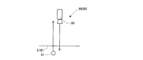
- the first transmission / scattering test 30 irradiates and transmits irradiation light, usually natural light, including linearly polarized light whose vibration plane is orthogonal to the absorption axis of the polarizer film, from one surface side to the polarizing film 3. Detects transmitted light and detects transmitted light that is transmitted through the other surface side of the polarizing film 3 including linearly polarized light whose vibration surface is orthogonal to the absorption axis, usually natural light, and transmitted. To do. That is, using the illumination 31 and the sensor 33 disposed above and below the polarizing film 3, the light emitted from the illumination 31 is transmitted and scattered and detected. In the first transmission / scattering inspection 30, as shown in FIG.
- the illuminations 31, 31 ′ and the sensors 33, 33 ′ corresponding to the illuminations 31, 33 ′ are arranged so as to face each other vertically with the polarizing film 3 interposed therebetween, or only one of the upper and lower sides, or If they are arranged only in the same direction, the amount of irradiated light is not enough to detect foreign matter on the back side of the illumination 31, or when the positions of foreign matter overlap on the upper and lower surfaces, etc. This is because it may not be possible to determine whether it exists on the surface.
- the light including the vibration plane orthogonal to the absorption axis of the polarizer can be, for example, an illumination 31 such as a fluorescent lamp, an LED, a metal halide lamp, or natural light.
- the sensor 33 for example, a line sensor camera, an area sensor camera, or the like can be used.
- the sensors 33 and 33 ′ are out of the optical axis of the irradiation light emitted from the illuminations 31 and 31 ′.
- the transmitted light is detected on an axis deviated from the optical axis of the irradiated light.
- the polarizing film 3 that has passed through the first cross transmission inspection 10, the first reflection / scattering inspection 20, and the first transmission / scattering inspection 30 in the first lamination process I flows on the line and proceeds to the second lamination process II.
- Other steps such as a step of laminating an optical film such as a retardation film may be inserted between the first laminating step I and the second laminating step II.
- the release film 4 is a film for protecting the pressure-sensitive adhesive layer applied to the polarizing film 3 from drying and foreign matters. That is, since the polarizing film 3 is used by being fixed to a liquid crystal display surface or the like, an adhesive layer is provided, and the release film 4 protects the adhesive layer until it is fixed to the liquid crystal panel. is there.
- the pressure-sensitive adhesive layer may be applied prior to laminating the polarizing film 3 on the polarizing film 3 in the first laminating step I or the polarizing film 3 in the second laminating step II, or as described above in advance. You may laminate
- the material of the release film 4 is not particularly limited.
- a film obtained by processing a thermoplastic resin polyethylene terephthalate, polyethylene naphtholate, polyethylene, polypropylene, etc.
- a thermoplastic resin polyethylene terephthalate, polyethylene naphtholate, polyethylene, polypropylene, etc.
- an adhesive used for an adhesive layer colorless and transparent adhesives, such as an acrylic adhesive, are mentioned, for example.
- the thickness of the pressure-sensitive adhesive layer is usually 5 to 50 ⁇ m, preferably 10 to 40 ⁇ m. When the thickness of the pressure-sensitive adhesive layer is 5 ⁇ m or less, the polarizer protective film 2 laminated via these layers is likely to be deformed by foreign matter, and therefore the inspection method of the present invention is preferably applied.
- the release film 4 has a thickness of usually 7 to 75 ⁇ m, preferably 15 to 40 ⁇ m.
- the protect film 5 is a film for protecting the surface of the polarizing film 3 from damage or abrasion.
- the protective film 5 is usually made of a transparent resin, and is laminated on the polarizing film 3 through an adhesive having weak adhesiveness until the polarizing film 3 is used, and is peeled off when the polarizing film 3 is used.
- This protective film 5 may be laminated on the polarizing film 3 simultaneously with the above-described release film 4 or may be laminated later.
- the transparent resin forming the protective film 5 is not particularly limited, and examples thereof include acrylic resins (polymethyl methacrylate, etc.), polyolefin resins (polyethylene, polypropylene, etc.), polyester resins (polyethylene terephthalate, polybutylene terephthalate, etc.), etc. Is mentioned.
- the protect film 5 may be a commercially available product.
- the thickness of the protect film 5 is usually 5 to 100 ⁇ m, preferably 30 to 50 ⁇ m.
- the thickness of the pressure-sensitive adhesive layer for laminating the protective film 5 on the polarizing film 3 is thin, air bubbles are likely to bite, and this may be mistaken as a bubble of the polarizing film 3, so the thickness of this pressure-sensitive adhesive layer is usually 5 ⁇ m or more.
- the polarizing film 3 laminated polarizing film 6 in which the release film 4 and the protective film 5 are laminated includes the second reflection / scattering inspection 40, the second transmission / scattering inspection 50, and the second cross transmission inspection. Continue on line to 60.
- the second reflection / scattering inspection 40 is obtained by arranging the first reflection / scattering inspection 20 shown in the first lamination step I on the upper and lower surface sides of the laminated polarizing film 6, and a pair of illuminations 41, 41 ′ and a sensor 43. , 43 ′, reflection scattering is performed from above and below the laminated polarizing film 6. Thereby, at least one of the unevenness
- the unevenness is caused by, for example, an abnormality at the time of bonding of the release film 4. At this time, as shown in FIG.
- the angle ⁇ formed by the incident light and the reflected light of the illuminations 41 and 41 ′ with respect to the laminated polarizing film 6 is preferably 60 to 120 °.
- the sensor 43, 43 ′ has an angle ⁇ of ⁇ 20 with respect to the line formed by regular reflection of the light irradiated to the inspection portion on the laminated polarizing film 6 from the illumination 41, 41 ′ with respect to the laminated polarizing film 6. It is installed with inclinations of ⁇ + 20 °, more preferably with inclinations of ⁇ 6 to ⁇ 2 ° and +2 to + 6 °, and the light reflected on the laminated polarizing film 6 is sensed and measured.
- the first transmission / scattering inspection 30 shown in the first lamination step I is arranged on only one of the upper and lower surfaces of the laminated polarizing film 6. Thereby, like the 1st transmission scattering test 30 shown in the 1st lamination process I, the foreign material on the lamination polarizing film 6, the clear bubble of a boundary, the sharp unevenness on the lamination polarizing film 6, etc. are detectable. Also in the second transmission / scattering inspection 50, as in the first transmission / scattering inspection 30, as shown in FIG.
- the senor 33 is off the optical axis of the irradiation light irradiated from the illumination 31, and normally It arrange
- the second cross transmission inspection 60 is an application of the same inspection as the first cross transmission inspection 10 shown in the first laminating step I to the laminated polarizing film 6, and transparent foreign matter (adhesive on the laminated polarizing film 6). The bright spots included etc.) can be detected.
- the illuminations 11 and 11 ′, the polarizing filters 12 and 12 ′, and the sensors 13 and 13 ′ corresponding to the illuminations 11 and 11 ′ face each other with the laminated polarizing film 6 interposed therebetween. Is arranged.
- the illumination 11, the polarizing filter 12 and the sensor 13 corresponding thereto are arranged with the laminated film 6 interposed therebetween, and (1) the linearly polarized light is irradiated from above the laminated film 6 and the transmitted light is emitted below. (2) Irradiation with linearly polarized light from the bottom of the laminated film 6 and detection of transmitted light may be detected above, or (3) Irradiation with linearly polarized light from the upper side of the laminated film 6 Then, the transmitted light may be detected from below by detecting linearly polarized light from below and detecting the transmitted light from below.
- a camera is used in each inspection of the first lamination step I and the second lamination step II.
- this camera preferably has a higher resolution in the order of sensor 13> sensor 33, 33 ′> sensor 23. This is because the concavo-convex defects detected in the first and second reflection scatter inspections are relatively large in size, and the bubble defects detected in the first and second transmission scatter inspections are relatively small in size, The foreign-material defect detected by the first and second cross transmission inspections corresponds to a smaller size.
- the resolution of the camera increases in the order of sensors 13, 13 ′> sensor 33> sensors 43, 43 ′>. The resolution of the camera is appropriately selected according to the size of the target foreign object, the processing speed of the camera, and the like.
- Sensors 13 and 13 ′ have a pixel range of 3 to 50 ⁇ m
- sensor 23 (43 and 43 ′) has a pixel range of 5 to 200 ⁇ m
- sensors 33 and 33 ′ have a pixel range of 4 to 50 ⁇ m. Selected.
- First cross transmission inspection 10 First reflection / scattering inspection 20, first transmission / scattering inspection 30 and second reflection / scattering inspection 40, second transmission / scattering inspection 50, second cross of second lamination process II Table 1 below shows the configuration, basic specifications, and detection target of the transmission inspection 60.
- the defect inspection method of the present invention can detect many defects in the laminated polarizing film.
- the laminated polarizing film 6 inspected by the second cross transmission inspection 60, the second reflection / scattering inspection 40, and the second transmission / scattering inspection 50 in the second lamination step II is then advanced to a cutting step, and is cut into a prescribed size. Those containing defects are removed as defective products.
- each defect detected by the inspection described above is sent to a marking device (not shown) such as a code printer or a marker provided during the first lamination process I or the second lamination process II by each sensor. And is printed on the edge of the polarizing film 3 or the laminated polarizing film 6.
- a marking device such as a code printer or a marker provided during the first lamination process I or the second lamination process II by each sensor.
- the laminated polarizing film 6 including the defective portion is removed by the marking printed on the release film 4 on the polarizing film 3.
- the present invention many kinds of defects can be dealt with by the minimum necessary inspection method in the polarizing film laminating process. Furthermore, because of the minimum necessary inspection method, the equipment of the polarizing film manufacturing apparatus is reduced, resulting in cost reduction. Furthermore, since the inspections can be performed in any order, the degree of freedom in the layout of the inspection process is increased.
Landscapes
- Physics & Mathematics (AREA)
- General Physics & Mathematics (AREA)
- Health & Medical Sciences (AREA)
- Engineering & Computer Science (AREA)
- Life Sciences & Earth Sciences (AREA)
- Chemical & Material Sciences (AREA)
- Analytical Chemistry (AREA)
- Biochemistry (AREA)
- General Health & Medical Sciences (AREA)
- Textile Engineering (AREA)
- Immunology (AREA)
- Pathology (AREA)
- Optics & Photonics (AREA)
- Polarising Elements (AREA)
- Investigating Materials By The Use Of Optical Means Adapted For Particular Applications (AREA)
Abstract
偏光子フィルム1に偏光子保護フィルム2が積層された偏光フィルム3を得る第一積層工程Iと、第一積層工程Iで得た偏光フィルム3の一方の表面側に離型フィルム4を積層すると共に、他方の表面側にプロテクトフィルム5を積層された積層偏光フィルム6を得る第二積層工程IIとを含む積層偏光フィルムの製造工程において、得られる積層偏光フィルムの欠陥検査方法であり、第一積層工程Iで得られる偏光フィルム3に対して行う第一クロス透過検査10、第一反射散乱検査20、第一透過散乱検査30と、第二積層工程IIで得られる積層偏光フィルム6に対して行う第二反射散乱検査40、第二透過散乱検査50、第二クロス透過検査60とを含む。
Description
本発明は、積層偏光フィルムの欠陥を検査する方法、製造方法および製造装置に関する。
偏光フィルムは、テレビなどの液晶表示装置において液晶セルの表面に貼合して使用される光学フィルムなどとして広く用いられている。このような偏光フィルムとしては、従来から、例えばポリビニルアルコール(PVA)系フィルムに二色性色素を吸着配向させて得られる偏光子フィルムに、トリアセチルセルロース(TAC)などからなる偏光子保護フィルムを積層したものが用いられる。
偏光フィルムは、その一方の表面に接着剤層を介して離型フィルム(セパレートフィルム)を、他方の表面にプロテクトフィルムをそれぞれ積層して、積層偏光フィルムとして出荷される。粘着剤層は、液晶セルの表面に貼合するためのものである。離型フィルムは、液晶セルに貼合するまで粘着剤層を保護するためのフィルムである。プロテクトフィルムは、偏光フィルムに傷がつくことを防止するためのフィルムである。
ところで、偏光フィルムに偏光子保護フィルムを積層する工程や、偏光フィルムに離型フィルムやプロテクトフィルムを積層する工程では、異物が混入したり、気泡が発生することなどがある。これらの異物や気泡などは積層偏光フィルムの欠陥となるため、従来より、このような欠陥を自動検査する検査方法が提案されている。
しかし、フィルムを積層する度に全ての欠陥を検査することは、生産性の点で不利である。この問題を解決するものとしては、例えば特許文献1に記載の検査方法が挙げられるが、かかる従来の検査方法ではフィルムに透明な異物が混入した場合に検出できない。
しかし、フィルムを積層する度に全ての欠陥を検査することは、生産性の点で不利である。この問題を解決するものとしては、例えば特許文献1に記載の検査方法が挙げられるが、かかる従来の検査方法ではフィルムに透明な異物が混入した場合に検出できない。
本発明の課題は、積層偏光フィルムの製造工程において、必要最小限の検査方法で、多くの種類の欠陥に対処できる積層偏光フィルムの欠陥検査方法を提供することである。
本発明の積層偏光フィルムの欠陥検査方法は、偏光子フィルムに偏光子保護フィルムを積層して偏光フィルムを得る第一積層工程と、前記第一積層工程により得た偏光フィルムの一方の表面側に粘着剤層を介して離型フィルムを積層すると共に、他方の表面側にプロテクトフィルムを積層して積層偏光フィルムを得る第二積層工程とを含む前記積層偏光フィルムの製造工程を経て得られる前記積層偏光フィルムの欠陥を検査する方法であり、
前記第一積層工程により得られた偏光フィルムに対して、一方の表面側から、振動面が前記偏光子フィルムの吸収軸に対して平行である直線偏光光を照射し、透過する透過光を検出する第一クロス透過検査と、
一方の表面側から、振動面が前記偏光子フィルムの吸収軸に対して直交する直線偏光光を含む光を照射し、該照射光の光軸から外れた軸上で透過光を検出すると共に、他方の表面側から、振動面が前記偏光子フィルムの吸収軸に対して直交する直線偏光光を含む照射光を照射し、透過する透過光を検出する第一透過散乱検査と、
一方の表面側から照射光を照射し、反射する反射光のうち、照射光の正反射方向から外れた方向に向かう反射光成分を検出する第一反射散乱検査とを行い、
前記第二積層工程により得られた積層偏光フィルムに対して、
一方の表面側から、振動面が前記偏光子フィルムの吸収軸に対して平行である直線偏光光を照射し、透過光を検出する第二クロス透過検査と、
一方の表面側から、振動面が前記偏光子フィルムの吸収軸に対して直交する直線偏光光を含む光を照射し、該直線偏光光の光軸から外れた軸上で透過光を検出する第二透過散乱検査と、
一方の表面側から照射光を照射し、反射する反射光のうち、照射光の正反射方向から外れた方向に向かう反射光成分を検出すると共に、他方の表面側から照射光を照射し、反射する反射光のうち、照射光の正反射方向から外れた方向に向かう反射光成分を検出する第二反射散乱検査とを行う。
前記第一積層工程により得られた偏光フィルムに対して、一方の表面側から、振動面が前記偏光子フィルムの吸収軸に対して平行である直線偏光光を照射し、透過する透過光を検出する第一クロス透過検査と、
一方の表面側から、振動面が前記偏光子フィルムの吸収軸に対して直交する直線偏光光を含む光を照射し、該照射光の光軸から外れた軸上で透過光を検出すると共に、他方の表面側から、振動面が前記偏光子フィルムの吸収軸に対して直交する直線偏光光を含む照射光を照射し、透過する透過光を検出する第一透過散乱検査と、
一方の表面側から照射光を照射し、反射する反射光のうち、照射光の正反射方向から外れた方向に向かう反射光成分を検出する第一反射散乱検査とを行い、
前記第二積層工程により得られた積層偏光フィルムに対して、
一方の表面側から、振動面が前記偏光子フィルムの吸収軸に対して平行である直線偏光光を照射し、透過光を検出する第二クロス透過検査と、
一方の表面側から、振動面が前記偏光子フィルムの吸収軸に対して直交する直線偏光光を含む光を照射し、該直線偏光光の光軸から外れた軸上で透過光を検出する第二透過散乱検査と、
一方の表面側から照射光を照射し、反射する反射光のうち、照射光の正反射方向から外れた方向に向かう反射光成分を検出すると共に、他方の表面側から照射光を照射し、反射する反射光のうち、照射光の正反射方向から外れた方向に向かう反射光成分を検出する第二反射散乱検査とを行う。
本発明によれば、積層偏光フィルムの製造工程において、必要最小限の検査により、多くの種類の欠陥に対処できる。しかも、離型フィルムおよびプロテクトフィルムを貼着する前後それぞれの工程において、各検査を順不同で行うことができるので、検査工程のレイアウトの自由度が高くなるという効果もある。
本発明に係る偏光フィルムの欠陥検査方法を、図1を用いて詳細に説明する。図1は、本発明に係る欠陥検査方法の一実施形態である自動検査装置100を示している。この自動検査装置100は、ポリビニルアルコール(PVA)系フィルムに二色性色素を吸着配向させて得られる偏光子フィルム1の上下面に接着剤層を介して偏光子保護フィルム2を積層することにより偏光フィルム3を得る第一積層工程Iと、この偏光フィルム3の一方の表面側に、予め粘着剤層が設けられた離型フィルム4を積層し、偏光フィルム3の他方の表面側にプロテクトフィルム5を積層することにより、積層偏光フィルム6を得る第二積層工程IIとに対して欠陥検査を行う。
(第一積層工程I)
第一積層工程Iでは、まず偏光子フィルム1の上下面の少なくとも一方の表面に偏光子保護フィルム2を積層して偏光フィルム3を得る。この偏光子フィルム1は、透過する光のうち、振動面が吸収軸に対して平行な直線偏光光は吸収して透過させず、振動面が吸収軸に対して直交する直線偏光光は、そのまま透過させる光学素子である。偏光子フィルム1を透過した光は、振動面が吸収軸に対して直交する直線偏光光である。
第一積層工程Iでは、まず偏光子フィルム1の上下面の少なくとも一方の表面に偏光子保護フィルム2を積層して偏光フィルム3を得る。この偏光子フィルム1は、透過する光のうち、振動面が吸収軸に対して平行な直線偏光光は吸収して透過させず、振動面が吸収軸に対して直交する直線偏光光は、そのまま透過させる光学素子である。偏光子フィルム1を透過した光は、振動面が吸収軸に対して直交する直線偏光光である。
前記偏光子フィルム1と偏光子保護フィルム2との積層する方法は特に限定されるものではなく、例えば接着剤層を介して積層すればよい。接着剤層を構成する接着剤としては、例えば、ビニルアルコール系ポリマーからなる接着剤、エポキシ系樹脂からなる接着剤、あるいは、少なくとも、ホウ酸やホウ砂、グルタルアルデヒドやメラミン、シュウ酸などのビニルアルコール系ポリマーの水溶性架橋剤からなる接着剤などが挙げられる。この接着剤としては、例えば、紫外線、電子線などの活性エネルギー線を照射されることにより硬化して偏光子フィルム1と偏光子保護フィルム2とを接着する、いわゆる活性エネルギー線硬化型接着剤も挙げられる。偏光子フィルム1の両面に偏光子保護フィルム2を積層する場合、両面とも同じ偏光子保護フィルム2であってもよく、異なる偏光子保護フィルム2であってもよい。例えば、偏光子フィルム1の両面に偏光子保護フィルム2としてトリアセチルセルロースフィルムを積層してもよく、片面のみにトリアセチルセルロースフィルムを積層してもよく、片面にトリアセチルセルロースフィルムを積層して他方の表面に他の偏光子保護フィルムを積層してもよい。また、偏光子保護フィルム2を偏光子フィルム1の片面に積層する場合、後述する第二積層工程IIにおいて、偏光子保護フィルム2の上にプロテクトフィルム5を貼着し、偏光子保護フィルム2を積層しない他方の表面側に粘着剤層および離型フィルム4をこの順に積層することが好ましい。
偏光子フィルム1の厚みは通常1~50μm、好ましくは3~20μmである。偏光子フィルム1の厚みが20μm以下であると、異物等の欠陥による偏光子フィルムの変形の影響が大きく現れるため、本発明の欠陥検査方法が好ましく適用される。接着剤層の厚みは通常0.1~5μm以下、好ましくは1μm以下である。
偏光子フィルム1の厚みは通常1~50μm、好ましくは3~20μmである。偏光子フィルム1の厚みが20μm以下であると、異物等の欠陥による偏光子フィルムの変形の影響が大きく現れるため、本発明の欠陥検査方法が好ましく適用される。接着剤層の厚みは通常0.1~5μm以下、好ましくは1μm以下である。
偏光子フィルム1の少なくとも一方の表面に設けられる偏光子保護フィルム2には、適宜な透明フィルムを用いることができる。中でも、透明性や機械的強度、熱安定性や水分遮蔽性等に優れるポリマーからなるフィルムが好ましく用いられる。そのポリマーとしては、アセテート系樹脂(例えば、トリアセチルセルロース(TAC)など)、ポリエステル系樹脂(例えば、ポリエチレンテレフタレート(PET)など)、アクリル系樹脂、ポリオレフィン系樹脂(例えば、ポリプロピレンなど)、環状ポリオレフィン系樹脂などが挙げられる。このようなフィルムは、キャスティング法、カレンダー法、押出し法のいずれで製造したものでもよいが、偏光特性や耐久性などの点から、トリアセチルセルロースのようなアセテート系樹脂が好ましく、特に表面をアルカリなどでケン化処理したトリアセチルセルロースフィルムが好ましい。偏光子保護フィルム2がアクリル系樹脂である場合、アクリル系樹脂は異物による極部的な変形により割れ易いため、本発明の方法が好ましく適用される。
偏光子保護フィルム2の厚みは通常5~100μm、好ましくは10~50μmである。
偏光子保護フィルム2の厚みは通常5~100μm、好ましくは10~50μmである。
本発明に係る第一積層工程Iでは、偏光子フィルム1に偏光子保護フィルム2を積層して偏光フィルム3を得た後、第一クロス透過検査10、第一反射散乱検査20、第一透過散乱検査30からなる3系列の検査を行う。偏光フィルム3は、下記に示す検査により欠陥を検出されながら、搬送ローラ(図示せず)により第二積層工程IIの方向へ流れていく。
なお、偏光子フィルム1に偏光子保護フィルム2を積層する前に、下記に示す第一透過散乱検査30と同じ検査を用いて、偏光子フィルム1上の異物を検出してもよい。
なお、偏光子フィルム1に偏光子保護フィルム2を積層する前に、下記に示す第一透過散乱検査30と同じ検査を用いて、偏光子フィルム1上の異物を検出してもよい。
<第一クロス透過検査10>
第一クロス透過検査10では、偏光フィルム3の上下どちらか一方に照明11、偏光フィルム3を挟んで反対側にセンサー13を配置し、照明11と偏光フィルム3の間に偏光フィルタ12を配置する。そして、前記偏光フィルム3に、一方の面側の照明11から偏光フィルタ12を介して、振動面が前記吸収軸に対して平行な直線偏光光を照射し、偏光フィルム3を透過する透過光をセンサー13にて検出することにより、偏光フィルム3の偏光子フィルム1より偏光フィルタ12側にある欠陥検出を行うものである。
偏光フィルタ12は、振動面が透過軸に対して平行である直線偏光光をそのまま透過し、直交する直線偏光光は通過しない光学フィルタである。偏光フィルタ12として通常は上記した偏光フィルム3と同様のものを用いることができる。偏光フィルタ12の吸収軸は、偏光フィルム3の吸収軸に対して直交させる。
クロス透過とは、前記偏光フィルム3とクロスニコルになるように偏光フィルタ12を配置し、これらの外側のいずれかの方向より、その他方の面に向けて、照明11からの光を照射することを指す。照明11からの光の入射側に異物があると光が散乱するなどして、振動面の方向が変わり、偏光子フィルム1を通過するので、偏光フィルム3中の偏光子フィルム1と偏光フィルタ12側との間にある透明な異物(輝点系)であっても、輝点としてセンサー13により検出される。
なお、第一クロス透過検査10の照明11は、第二積層工程IIにおいて離型フィルム4を積層する側から照射するのが好ましい。透過光は通常、図3に示すように、照射される直線偏光光の光軸と同じ軸上で検出する。
上記した照明11としては、例えば蛍光灯、LED、メタルハライドランプ等が使用可能であり、より好ましくはメタルハライドランプがよい。センサー13としては、例えばラインセンサーカメラ、エリアセンサーカメラ等が使用可能である。
第一クロス透過検査10では、偏光フィルム3の上下どちらか一方に照明11、偏光フィルム3を挟んで反対側にセンサー13を配置し、照明11と偏光フィルム3の間に偏光フィルタ12を配置する。そして、前記偏光フィルム3に、一方の面側の照明11から偏光フィルタ12を介して、振動面が前記吸収軸に対して平行な直線偏光光を照射し、偏光フィルム3を透過する透過光をセンサー13にて検出することにより、偏光フィルム3の偏光子フィルム1より偏光フィルタ12側にある欠陥検出を行うものである。
偏光フィルタ12は、振動面が透過軸に対して平行である直線偏光光をそのまま透過し、直交する直線偏光光は通過しない光学フィルタである。偏光フィルタ12として通常は上記した偏光フィルム3と同様のものを用いることができる。偏光フィルタ12の吸収軸は、偏光フィルム3の吸収軸に対して直交させる。
クロス透過とは、前記偏光フィルム3とクロスニコルになるように偏光フィルタ12を配置し、これらの外側のいずれかの方向より、その他方の面に向けて、照明11からの光を照射することを指す。照明11からの光の入射側に異物があると光が散乱するなどして、振動面の方向が変わり、偏光子フィルム1を通過するので、偏光フィルム3中の偏光子フィルム1と偏光フィルタ12側との間にある透明な異物(輝点系)であっても、輝点としてセンサー13により検出される。
なお、第一クロス透過検査10の照明11は、第二積層工程IIにおいて離型フィルム4を積層する側から照射するのが好ましい。透過光は通常、図3に示すように、照射される直線偏光光の光軸と同じ軸上で検出する。
上記した照明11としては、例えば蛍光灯、LED、メタルハライドランプ等が使用可能であり、より好ましくはメタルハライドランプがよい。センサー13としては、例えばラインセンサーカメラ、エリアセンサーカメラ等が使用可能である。
前記第一クロス透過検査10で照射され、偏光フィルタ12を介して偏光フィルムに照射される光は、偏光フィルタ12の吸収軸に対して直交する振動面を有する直線偏光光であり、平行な振動面を有する直線偏光成分は含まない(後述する第二クロス透過検査60も同様である)。
平行な偏光成分と直交する偏光成分との比率を示す視感度補正偏光度(Py)は、下記の計算式(1)により求められる。この視感度補正偏光度(Py)は、通常98%以上、理想的には100%である。
平行な偏光成分と直交する偏光成分との比率を示す視感度補正偏光度(Py)は、下記の計算式(1)により求められる。この視感度補正偏光度(Py)は、通常98%以上、理想的には100%である。
偏光フィルムの光学特性を、積分球付き分光光度計(日本分光株式会社製、V7100)にて測定する。波長380nm~780nmの範囲においてMD透過率とTD透過率を求め、式(1)に基づいて各波長における偏光度を算出し、さらにJIS Z 8701の2度視野(C光源)により視感度補正を行い、視感度補正偏光度(Py)を求める。
上記において、「MD透過率」とは、グラントムソンプリズムから出る直線偏光光の振動面の向きと偏光板サンプルの透過軸を平行にしたときの透過率であり、式(1)においては「MD」と表す。「TD透過率」とは、グラントムソンプリズムから出る直線偏光光の振動面の向きと偏光板サンプルの透過軸を直交にしたときの透過率であり、式(1)においては「TD」と表す。
偏光度(%)={(MD-TD)/(MD+TD)}1/2×100 式(1)
<第一反射散乱検査20>
第一積層工程Iに示す第一反射散乱検査20は、偏光フィルム3に対して、斜めに配置した照明21から偏光フィルム3上に光を照射し、偏光子フィルム1上で反射する反射光のうち、照射した光の正反射方向から外れた方向に向かう反射光成分をセンサー23によって読み取り、偏光フィルム3の偏光子フィルム1と偏光子保護フィルム2との間、あるいは偏光子保護フィルム2上に発生した気泡や偏光フィルム3上の凹凸を検出するものである。この時、図4に示すように、偏光フィルム3に対する照明21の入射光と反射光のなす角度αは60~120°であるのがよい。またセンサー23は偏光フィルム3に対し、照明21から偏光フィルム3上の検査部に照射された光が正反射してなす線に対しての角度βが-20~+20°の傾き、さらに好ましくは-6~-2°と+2~+6°の傾きで設置される。このセンサー23は、偏光フィルム3に照射されて反射した光線を感知して測定する。
欠陥検出手段20は、偏光フィルム3の上下面の少なくとも一方に設置すればよく、好ましくは上下面のいずれか一方に設置され、さらに好ましくは、後工程にて粘着剤層が設けられた離型フィルム4を積層する側に設置される。
上記した照明21としては、例えば蛍光灯、LED、メタルハライドランプ等が使用可能である。センサー23としては、例えばラインセンサーカメラ、エリアセンサーカメラ等が使用可能である。
第一積層工程Iに示す第一反射散乱検査20は、偏光フィルム3に対して、斜めに配置した照明21から偏光フィルム3上に光を照射し、偏光子フィルム1上で反射する反射光のうち、照射した光の正反射方向から外れた方向に向かう反射光成分をセンサー23によって読み取り、偏光フィルム3の偏光子フィルム1と偏光子保護フィルム2との間、あるいは偏光子保護フィルム2上に発生した気泡や偏光フィルム3上の凹凸を検出するものである。この時、図4に示すように、偏光フィルム3に対する照明21の入射光と反射光のなす角度αは60~120°であるのがよい。またセンサー23は偏光フィルム3に対し、照明21から偏光フィルム3上の検査部に照射された光が正反射してなす線に対しての角度βが-20~+20°の傾き、さらに好ましくは-6~-2°と+2~+6°の傾きで設置される。このセンサー23は、偏光フィルム3に照射されて反射した光線を感知して測定する。
欠陥検出手段20は、偏光フィルム3の上下面の少なくとも一方に設置すればよく、好ましくは上下面のいずれか一方に設置され、さらに好ましくは、後工程にて粘着剤層が設けられた離型フィルム4を積層する側に設置される。
上記した照明21としては、例えば蛍光灯、LED、メタルハライドランプ等が使用可能である。センサー23としては、例えばラインセンサーカメラ、エリアセンサーカメラ等が使用可能である。
<第一透過散乱検査30>
第一透過散乱検査30は、一方の表面側から偏光フィルム3に、振動面が前記偏光子フィルムの吸収軸に対して直交する直線偏光光を含む照射光、通常は自然光を照射し、透過する透過光を検出すると共に、前記偏光フィルム3の他方の表面側から、振動面が前記吸収軸に対して直交する直線偏光光を含む照射光、通常は自然光を照射し、透過する透過光を検出する。すなわち、偏光フィルム3を挟んで上下に配置された照明31とセンサー33とを用いて、照明31より照射した光を透過散乱させて検出する。第一透過散乱検査30において、図1に示すように、照明31、31’とこれに対応するセンサー33、33’とは一対ずつ二基配置されている。これによって偏光フィルム3における偏光子フィルム1の上面と偏光子保護フィルム2との間、あるいは偏光子フィルム1の下面と偏光子保護フィルム2との間という二箇所の異物をより確実に検出でき、さらに境目の明瞭な気泡や偏光フィルム3上の鋭い凹凸も検出することが可能になる。第一透過散乱検査30において、照明31、31’とこれに対応するセンサー33、33’とを、偏光フィルム3を挟んで上下にそれぞれ対向するよう配置するのは、上下どちらか一方のみ、または同一方向にしか配置しない場合、照射された光量が足りず照明31の裏側にある異物を検出できなかったり、また上下面で異物同士の位置が重なっていた時等、偏光フィルム3の上下どちらの面に存在するかが判断できなかったりするおそれがあるためである。
なお、前記偏光子の吸収軸に対して直交する振動面を含む光は、例えば蛍光灯、LED、メタルハライドランプ等の照明31、あるいは自然光が使用可能である。センサー33としては、例えばラインセンサーカメラ、エリアセンサーカメラ等が使用可能である。
また、この第一透過散乱検査30においては、図2に示すように、センサー33、33’が、照明31、31’から照射される照射光の光軸から外れており、通常はこの光軸と平行な軸上に配置され、透過光はこの照射光の光軸から外れた軸上で検出される。
第一透過散乱検査30は、一方の表面側から偏光フィルム3に、振動面が前記偏光子フィルムの吸収軸に対して直交する直線偏光光を含む照射光、通常は自然光を照射し、透過する透過光を検出すると共に、前記偏光フィルム3の他方の表面側から、振動面が前記吸収軸に対して直交する直線偏光光を含む照射光、通常は自然光を照射し、透過する透過光を検出する。すなわち、偏光フィルム3を挟んで上下に配置された照明31とセンサー33とを用いて、照明31より照射した光を透過散乱させて検出する。第一透過散乱検査30において、図1に示すように、照明31、31’とこれに対応するセンサー33、33’とは一対ずつ二基配置されている。これによって偏光フィルム3における偏光子フィルム1の上面と偏光子保護フィルム2との間、あるいは偏光子フィルム1の下面と偏光子保護フィルム2との間という二箇所の異物をより確実に検出でき、さらに境目の明瞭な気泡や偏光フィルム3上の鋭い凹凸も検出することが可能になる。第一透過散乱検査30において、照明31、31’とこれに対応するセンサー33、33’とを、偏光フィルム3を挟んで上下にそれぞれ対向するよう配置するのは、上下どちらか一方のみ、または同一方向にしか配置しない場合、照射された光量が足りず照明31の裏側にある異物を検出できなかったり、また上下面で異物同士の位置が重なっていた時等、偏光フィルム3の上下どちらの面に存在するかが判断できなかったりするおそれがあるためである。
なお、前記偏光子の吸収軸に対して直交する振動面を含む光は、例えば蛍光灯、LED、メタルハライドランプ等の照明31、あるいは自然光が使用可能である。センサー33としては、例えばラインセンサーカメラ、エリアセンサーカメラ等が使用可能である。
また、この第一透過散乱検査30においては、図2に示すように、センサー33、33’が、照明31、31’から照射される照射光の光軸から外れており、通常はこの光軸と平行な軸上に配置され、透過光はこの照射光の光軸から外れた軸上で検出される。
第一積層工程Iの第一クロス透過検査10,第一反射散乱検査20,第一透過散乱検査30を経た偏光フィルム3はライン上を流れ、第二積層工程IIへと進む。
前記第一積層工程Iと第二積層工程IIとの間には、例えば、位相差フィルム等の光学フィルムを積層する工程等の他の工程が入ってもよい。
前記第一積層工程Iと第二積層工程IIとの間には、例えば、位相差フィルム等の光学フィルムを積層する工程等の他の工程が入ってもよい。
(第二積層工程II)
第二積層工程IIにおいては、まず偏光フィルム3に粘着剤層が設けられた離型フィルム4および/またはプロテクトフィルム5を貼着し、積層偏光フィルム6を作成する。
第二積層工程IIにおいては、まず偏光フィルム3に粘着剤層が設けられた離型フィルム4および/またはプロテクトフィルム5を貼着し、積層偏光フィルム6を作成する。
離型フィルム4は、偏光フィルム3に塗工された粘着剤層を乾燥・異物などから保護するためのフィルムである。すなわち、偏光フィルム3は、液晶表示面などに固着して使用するため、粘着剤層が設けられており、その粘着剤層を液晶パネルに固着させるまでの間保護するのが離型フィルム4である。前記粘着剤層は、第一積層工程Iで偏光フィルム3あるいは第二積層工程IIで離型フィルム4を偏光フィルム3に積層する前に塗工してもよいし、あるいは上記のように、予め離型フィルム4に塗工した状態で偏光フィルム3に積層してもよい。
離型フィルム4の材質は特に限定されず、例えば、熱可塑性樹脂(ポリエチレンテレフタレート、ポリエチレンナフトレート、ポリエチレン、ポリプロピレンなど)などを加工して得られるフィルムに、粘着剤層から剥離しやすくなるような処理を施したフィルムなどが挙げられる。粘着剤層に使用される粘着剤としては、例えば、アクリル系粘着剤などの無色透明な粘着剤が挙げられる。
前記粘着剤層の厚みは通常5~50μm、好ましくは10~40μmである。粘着剤層の厚みが5μm以下であると、これらを介して積層される偏光子保護フィルム2が異物により変形しやすくなることから、本発明の検査方法が好ましく適用される。また、前記離型フィルム4の厚みは通常7~75μm、好ましくは15~40μmである。
離型フィルム4の材質は特に限定されず、例えば、熱可塑性樹脂(ポリエチレンテレフタレート、ポリエチレンナフトレート、ポリエチレン、ポリプロピレンなど)などを加工して得られるフィルムに、粘着剤層から剥離しやすくなるような処理を施したフィルムなどが挙げられる。粘着剤層に使用される粘着剤としては、例えば、アクリル系粘着剤などの無色透明な粘着剤が挙げられる。
前記粘着剤層の厚みは通常5~50μm、好ましくは10~40μmである。粘着剤層の厚みが5μm以下であると、これらを介して積層される偏光子保護フィルム2が異物により変形しやすくなることから、本発明の検査方法が好ましく適用される。また、前記離型フィルム4の厚みは通常7~75μm、好ましくは15~40μmである。
プロテクトフィルム5は、偏光フィルム3の表面を損傷や摩耗などから保護するためのフィルムである。プロテクトフィルム5は、通常、透明樹脂からなり、偏光フィルム3の使用時まで弱い粘着性を有する粘着剤を介して偏光フィルム3に積層されており、偏光フィルム3の使用時には剥離される。このプロテクトフィルム5は、上記した離型フィルム4と同時に偏光フィルム3へ積層してもよいし、後で積層してもよい。
プロテクトフィルム5を形成する透明樹脂は特に限定されず、例えば、アクリル系樹脂(ポリメタクリル酸メチルなど)、ポリオレフィン系樹脂(ポリエチレン、ポリプロピレンなど)、ポリエステル系樹脂(ポリエチレンテレフタレート、ポリブチレンテレフタレートなど)などが挙げられる。
なお、プロテクトフィルム5は市販品を用いてもよく、例えば、「マスタック(藤森工業(株)製)」、「サニテクト((株)サンエー化研製)」、「イーマスク(日東電工(株)製)」、「トレテック(東レフィルム加工(株)製)」などが市販されている。前記プロテクトフィルム5の厚みは通常5~100μm、好ましくは30~50μmである。プロテクトフィルム5を偏光フィルム3に積層するための粘着剤層の厚みが薄いと、気泡をかみ込み易く、これが偏光フィルム3の気泡と誤認されることがあるため、この粘着剤層の厚みは通常5μm以上である。
プロテクトフィルム5を形成する透明樹脂は特に限定されず、例えば、アクリル系樹脂(ポリメタクリル酸メチルなど)、ポリオレフィン系樹脂(ポリエチレン、ポリプロピレンなど)、ポリエステル系樹脂(ポリエチレンテレフタレート、ポリブチレンテレフタレートなど)などが挙げられる。
なお、プロテクトフィルム5は市販品を用いてもよく、例えば、「マスタック(藤森工業(株)製)」、「サニテクト((株)サンエー化研製)」、「イーマスク(日東電工(株)製)」、「トレテック(東レフィルム加工(株)製)」などが市販されている。前記プロテクトフィルム5の厚みは通常5~100μm、好ましくは30~50μmである。プロテクトフィルム5を偏光フィルム3に積層するための粘着剤層の厚みが薄いと、気泡をかみ込み易く、これが偏光フィルム3の気泡と誤認されることがあるため、この粘着剤層の厚みは通常5μm以上である。
第二積層工程IIにおいて、離型フィルム4とプロテクトフィルム5とが積層された偏光フィルム3(積層偏光フィルム6)は、第二反射散乱検査40,第二透過散乱検査50,第二クロス透過検査60へとライン上を進む。
<第二反射散乱検査40>
第二反射散乱検査40は、第一積層工程Iに示した第一反射散乱検査20を積層偏光フィルム6の上下それぞれの表面側に配置したものであり、一対の照明41,41’とセンサー43,43’とにより積層偏光フィルム6の上下から反射散乱を行う。これにより、積層偏光フィルム6の上下面での凹凸やスジの少なくとも一つを検出する。凹凸は、例えば離型フィルム4の貼合時の異常等に起因するものである。
この時、図4に示すように、積層偏光フィルム6に対する照明41,41’の入射光と反射光のなす角度αは60~120°であるのがよい。センサー43,43’は、積層偏光フィルム6に対し、照明41,41’から積層偏光フィルム6上の検査部に照射された光が正反射してなす線に対してのなす角度βは-20~+20°の傾き、さらに好ましくは-6~-2°と+2~+6°の傾きで設置され、積層偏光フィルム6に照射されて反射した光線を感知して測定する。
第二反射散乱検査40は、第一積層工程Iに示した第一反射散乱検査20を積層偏光フィルム6の上下それぞれの表面側に配置したものであり、一対の照明41,41’とセンサー43,43’とにより積層偏光フィルム6の上下から反射散乱を行う。これにより、積層偏光フィルム6の上下面での凹凸やスジの少なくとも一つを検出する。凹凸は、例えば離型フィルム4の貼合時の異常等に起因するものである。
この時、図4に示すように、積層偏光フィルム6に対する照明41,41’の入射光と反射光のなす角度αは60~120°であるのがよい。センサー43,43’は、積層偏光フィルム6に対し、照明41,41’から積層偏光フィルム6上の検査部に照射された光が正反射してなす線に対してのなす角度βは-20~+20°の傾き、さらに好ましくは-6~-2°と+2~+6°の傾きで設置され、積層偏光フィルム6に照射されて反射した光線を感知して測定する。
<第二透過散乱検査50>
第二積層工程IIにおける第二透過散乱検査50は、第一積層工程Iに示した第一透過散乱検査30を積層偏光フィルム6の上下面のどちらか一方だけに配置したものである。
これにより、第一積層工程Iに示す第一透過散乱検査30と同じく、積層偏光フィルム6上の異物、境目の明瞭な気泡および積層偏光フィルム6上の鋭い凹凸等を検出することができる。
また、この第二透過散乱検査50においても、第一透過散乱検査30と同様、図2に示すように、センサー33が、照明31から照射される照射光の光軸から外れており、通常はこの光軸と平行な軸上に配置され、透過光はこの照射光の光軸から外れた軸上で検出される。
第二積層工程IIにおける第二透過散乱検査50は、第一積層工程Iに示した第一透過散乱検査30を積層偏光フィルム6の上下面のどちらか一方だけに配置したものである。
これにより、第一積層工程Iに示す第一透過散乱検査30と同じく、積層偏光フィルム6上の異物、境目の明瞭な気泡および積層偏光フィルム6上の鋭い凹凸等を検出することができる。
また、この第二透過散乱検査50においても、第一透過散乱検査30と同様、図2に示すように、センサー33が、照明31から照射される照射光の光軸から外れており、通常はこの光軸と平行な軸上に配置され、透過光はこの照射光の光軸から外れた軸上で検出される。
<第二クロス透過検査60>
第二クロス透過検査60は、第一積層工程Iに示す第一クロス透過検査10と同様の検査を積層偏光フィルム6に適用したものであり、積層偏光フィルム6上の透明な異物(粘着剤に含まれる輝点等)を検出することができる。
図1に示す第二クロス透過検査60においては、照明11、11’と偏光フィルタ12、12’とこれに対応するセンサー13、13’とを、積層偏光フィルム6を挟んで上下にそれぞれ対向するよう配置している。さらに、照明11と偏光フィルタ12とこれに対応するセンサー13とは、積層フィルム6を挟んで配置して、(1)積層フィルム6の上から直線偏光光を照射して、下で透過光を検出してもよいし、(2)積層フィルム6の下から直線偏光光を照射して、上で透過光を検出してもよいし、(3)積層フィルム6の上から直線偏光光を照射して、下で透過光を検出すると共に、下からも直線偏光光を照射して、上から透過光を検出してもよい。
第二クロス透過検査60は、第一積層工程Iに示す第一クロス透過検査10と同様の検査を積層偏光フィルム6に適用したものであり、積層偏光フィルム6上の透明な異物(粘着剤に含まれる輝点等)を検出することができる。
図1に示す第二クロス透過検査60においては、照明11、11’と偏光フィルタ12、12’とこれに対応するセンサー13、13’とを、積層偏光フィルム6を挟んで上下にそれぞれ対向するよう配置している。さらに、照明11と偏光フィルタ12とこれに対応するセンサー13とは、積層フィルム6を挟んで配置して、(1)積層フィルム6の上から直線偏光光を照射して、下で透過光を検出してもよいし、(2)積層フィルム6の下から直線偏光光を照射して、上で透過光を検出してもよいし、(3)積層フィルム6の上から直線偏光光を照射して、下で透過光を検出すると共に、下からも直線偏光光を照射して、上から透過光を検出してもよい。
前記第一積層工程Iおよび第二積層工程IIの各検査ではカメラを使用する。このカメラは、前記第一積層工程Iにおいて好ましくは、センサー13>センサー33、33’>センサー23の順で解像度が高くなる。これは第一および第二反射散乱検査で検出される凹凸系の欠陥は、サイズが比較的大きく、第一および第二透過散乱検査で検出される気泡系の欠陥は、サイズが比較的小さく、第一および第二クロス透過検査で検出される異物系欠陥は、更にサイズが小さいことに対応するものである。前記第二積層工程IIにおいては、センサー13、13’>センサー33>センサー43、43’>の順でカメラの解像度が高くなる。
前記カメラの解像度は、目的の異物の大きさ、カメラの処理スピード、等に応じて適宜選択される。センサー13、13’は1画素で3~50μmの範囲、センサー23(43、43’)は1画素で5~200μmの範囲、センサー33、33’が1画素で4~50μmの範囲となるように選択される。
前記カメラの解像度は、目的の異物の大きさ、カメラの処理スピード、等に応じて適宜選択される。センサー13、13’は1画素で3~50μmの範囲、センサー23(43、43’)は1画素で5~200μmの範囲、センサー33、33’が1画素で4~50μmの範囲となるように選択される。
第一積層工程Iの第一クロス透過検査10,第一反射散乱検査20,第一透過散乱検査30および第二積層工程IIの第二反射散乱検査40,第二透過散乱検査50,第二クロス透過検査60について、構成、基本仕様および検出対象を下記の表1に示す。
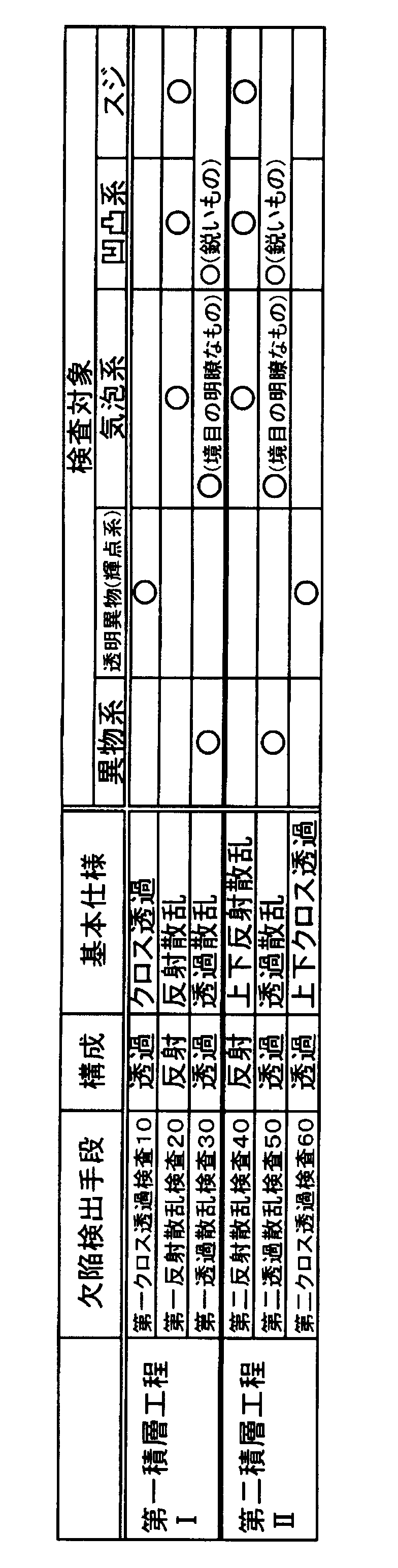
表1によると、本発明の欠陥検査方法が、積層偏光フィルムにおいて、多くの欠陥を検出可能であることがわかる。
上記した第一積層工程Iの第一クロス透過検査10,第一反射散乱検査20,第一透過散乱検査30および第二積層工程IIの第二クロス透過検査60,第二反射散乱検査40,第二透過散乱検査50は、それぞれの積層工程の中で用いるならば、特に設置する順序は限定されない。
第二積層工程IIにおける第二クロス透過検査60,第二反射散乱検査40,第二透過散乱検査50により検査された積層偏光フィルム6は、次に切断工程に進み、規定の大きさに切断され、欠陥を含むものは不良品として除去される。
上記した検査によって検出されたそれぞれの欠陥の位置は、それぞれのセンサーにより、第一積層工程Iまたは第二積層工程II中に設けられたコードプリンターやマーカー等のマーキング装置(図示せず)へ送られ、偏光フィルム3あるいは積層偏光フィルム6の端部等に印字される。そして切断工程の際、偏光フィルム3上の剥離フィルム4上に印字されたマーキングにより、不良部分を含む積層偏光フィルム6は除去される。
本発明によると、偏光フィルムの積層工程において、必要最小限の検査方法で、多くの種類の欠陥に対処できる。さらに、必要最小限の検査方法のため、偏光フィルムの製造装置の設備が小さくなり、コスト削減になる。さらに、各検査を順不同で行うことができるので、検査工程のレイアウトの自由度が高くなる。
以上、本発明の積層偏光フィルムの欠陥を検査する方法、製造方法および製造装置の好適な実施形態について説明したが、本発明はこのような実施形態のみに制限されるものではなく、種々の改良や改善が可能であることは言うまでもない。
Claims (10)
- 偏光子フィルムに偏光子保護フィルムを積層して偏光フィルムを得る第一積層工程と、
前記第一積層工程により得た偏光フィルムの一方の表面側に粘着剤層を介して離型フィルムを積層すると共に、他方の表面側にプロテクトフィルムを積層して積層偏光フィルムを得る第二積層工程と
を含む前記積層偏光フィルムの製造工程を経て得られる前記積層偏光フィルムの欠陥を検査する方法であり、
前記第一積層工程により得られた偏光フィルムに対して、
一方の表面側から、振動面が前記偏光子フィルムの吸収軸に対して平行である直線偏光光を照射し、透過する透過光を検出する第一クロス透過検査と、
一方の表面側から、振動面が前記偏光子フィルムの吸収軸に対して直交する直線偏光光を含む光を照射し、該照射光の光軸から外れた軸上で透過光を検出すると共に、他方の表面側から、振動面が前記偏光子フィルムの吸収軸に対して直交する直線偏光光を含む照射光を照射し、透過する透過光を検出する第一透過散乱検査と、
一方の表面側から照射光を照射し、反射する反射光のうち、照射光の正反射方向から外れた方向に向かう反射光成分を検出する第一反射散乱検査とを行い、
前記第二積層工程により得られた積層偏光フィルムに対して、
一方の表面側から、振動面が前記偏光子フィルムの吸収軸に対して平行である直線偏光光を照射し、透過光を検出する第二クロス透過検査と、
一方の表面側から、振動面が前記偏光子フィルムの吸収軸に対して直交する直線偏光光を含む光を照射し、該直線偏光光の光軸から外れた軸上で透過光を検出する第二透過散乱検査と、
一方の表面側から照射光を照射し、反射する反射光のうち、照射光の正反射方向から外れた方向に向かう反射光成分を検出すると共に、他方の表面側から照射光を照射し、反射する反射光のうち、照射光の正反射方向から外れた方向に向かう反射光成分を検出する第二反射散乱検査とを行うことを特徴とする前記積層偏光フィルムの欠陥検査方法。 - 第二クロス透過検査において更に、他方の表面側から、振動面が前記偏光子フィルムの吸収軸に対して平行である直線偏光光を照射し、透過光を検出する請求項1に記載の欠陥検査方法。
- 前記第一クロス透過検査、第一透過散乱検査および第一反射散乱検査によって、偏光フィルムの内部および表面における不透明異物、気泡、凹凸、スジおよび透明異物を欠陥として検出することを特徴とする請求項1または2に記載の積層偏光フィルムの欠陥検査方法。
- 前記第二クロス透過検査、第二透過散乱検査および第二反射散乱検査によって、積層偏光フィルムの内部および表面における不透明異物、気泡、凹凸、スジおよび透明異物を欠陥として検出することを特徴とする請求項1~3のいずれかに記載の積層偏光フィルムの欠陥検査方法。
- 前記第一透過散乱検査および第二透過散乱検査において、照射光の光軸より2~6mm外れた軸上でセンサーが異物を検出することを特徴とする請求項1~4のいずれかに記載の積層偏光フィルムの欠陥検査方法。
- 第一クロス透過検査における透過光を検出するためのセンサー、第一透過散乱検査における透過光を検出するためのセンサー、および第一反射散乱検査における前記反射光成分を検出するためのセンサーとしてカメラが使用され、第一反射散乱検査、第一透過散乱検査、第一クロス透過検査の順で該カメラの解像度が高くなっており、第二クロス透過検査における透過光を検出するためのセンサー、第二透過散乱検査における透過光を検出するためのセンサー、および第二反射散乱検査における前記反射光成分を検出するためのセンサーとしてカメラが使用され、第二反射散乱検査、第二透過散乱検査、第二クロス透過検査の順で、カメラの解像度が高くなっていることを特徴とする請求項1~5のいずれかに記載の積層偏光フィルムの欠陥検査方法。
- 偏光子フィルムに偏光子保護フィルムを積層して偏光フィルムを得る第一積層工程と、
前記第一積層工程により得た偏光フィルムの一方の表面側に粘着剤層を介して離型フィルムを積層すると共に、他方の表面側にプロテクトフィルムを積層して積層偏光フィルムを得る第二積層工程と
を含む前記積層偏光フィルムの製造方法であり、
前記第一積層工程により得られた偏光フィルムに対して、
一方の表面側から、振動面が前記偏光子フィルムの吸収軸に対して平行である直線偏光光を照射し、透過する透過光を検出する第一クロス透過検査工程と、
一方の表面側から、振動面が前記偏光子フィルムの吸収軸に対して直交する直線偏光光を含む光を照射し、透過光を検出すると共に、他方の表面側から、振動面が前記偏光子フィルムの吸収軸に対して直交する直線偏光光を含む光を照射し、透過する透過光を検出する第一透過散乱検査工程と、
一方の表面側から照射光を照射し、反射する反射光のうち、照射光の正反射方向から外れた方向に向かう反射光成分を検出する第一反射散乱検査工程と
を行い、
前記第二積層工程により得られた積層偏光フィルムに対して、
一方の表面側から、振動面が前記偏光子フィルムの吸収軸に対して平行である直線偏光光を照射し、透過光を検出する第二クロス透過検査工程と、
一方の表面側から、振動面が前記偏光子フィルムの吸収軸に対して直交する直線偏光光を含む光を照射し、透過光を検出する第二透過散乱検査工程と、
一方の表面側から照射光を照射し、反射する反射光のうち、照射光の正反射方向から外れた方向に向かう反射光成分を検出すると共に、他方の表面側から照射光を照射し、反射する反射光のうち、照射光の正反射方向から外れた方向に向かう反射光成分を検出する第二反射散乱検査工程と
を行うことを特徴とする前記積層偏光フィルムの製造方法。 - 第二クロス透過検査工程において、更に他方の表面側から、振動面が前記偏光子フィルムの吸収軸に対して平行である直線偏光光を照射し、透過光を検出する請求項7に記載の製造方法。
- 偏光子フィルムに偏光子保護フィルムを積層して偏光フィルムを得る第一積層手段と、
前記第一積層手段により得た偏光フィルムの一方の表面側に粘着剤層を介して離型フィルムを積層すると共に、他方の表面側にプロテクトフィルムを積層して積層偏光フィルムを得る第二積層手段と
を含む前記積層偏光フィルムの製造装置であり、
前記第一積層手段により得られた偏光フィルムに対して、
一方の表面側から、振動面が前記偏光子フィルムの吸収軸に対して平行である直線偏光光を照射し、透過する透過光を検出する第一クロス透過検出手段と、
一方の表面側から、振動面が前記偏光子フィルムの吸収軸に対して直交する直線偏光光を含む光を照射し、透過光を検出すると共に、他方の表面側から、振動面が前記偏光子フィルムの吸収軸に対して直交する直線偏光光を含む光を照射し、透過する透過光を検出する第一透過散乱検出手段と、
一方の表面側から照射光を照射し、反射する反射光のうち、照射光の正反射方向から外れた方向に向かう反射光成分を検出する第一反射散乱検出手段と
を備え、
前記第二積層工程により得られた積層偏光フィルムに対して、
一方の表面側から、振動面が前記偏光子フィルムの吸収軸に対して平行である直線偏光光を照射し、透過光を検出する第二クロス透過検出手段と、
一方の表面側から、振動面が前記偏光子フィルムの吸収軸に対して直交する直線偏光光を含む光を照射し、透過光を検出する第二透過散乱検出手段と、
一方の表面側から照射光を照射し、反射する反射光のうち、照射光の正反射方向から外れた方向に向かう反射光成分を検出すると共に、他方の表面側から照射光を照射し、反射する反射光のうち、照射光の正反射方向から外れた方向に向かう反射光成分を検出する第二反射散乱検出手段と
を備えることを特徴とする前記積層偏光フィルムの製造装置。 - 第二クロス透過検出手段はさらに、他方の表面側から、振動面が前記偏光子フィルムの吸収軸に対して平行である直線偏光光を照射し、透過光を検出する手段である請求項9に記載の製造装置。
Applications Claiming Priority (2)
| Application Number | Priority Date | Filing Date | Title |
|---|---|---|---|
| JP2014111598A JP2015225041A (ja) | 2014-05-29 | 2014-05-29 | 積層偏光フィルムの欠陥検査方法 |
| JP2014-111598 | 2014-05-29 |
Publications (1)
| Publication Number | Publication Date |
|---|---|
| WO2015182541A1 true WO2015182541A1 (ja) | 2015-12-03 |
Family
ID=54698871
Family Applications (1)
| Application Number | Title | Priority Date | Filing Date |
|---|---|---|---|
| PCT/JP2015/064873 Ceased WO2015182541A1 (ja) | 2014-05-29 | 2015-05-25 | 積層偏光フィルムの欠陥検査方法、製造方法および製造装置 |
Country Status (3)
| Country | Link |
|---|---|
| JP (1) | JP2015225041A (ja) |
| TW (1) | TW201610419A (ja) |
| WO (1) | WO2015182541A1 (ja) |
Cited By (3)
| Publication number | Priority date | Publication date | Assignee | Title |
|---|---|---|---|---|
| CN113906287A (zh) * | 2019-06-07 | 2022-01-07 | 杉金光电(苏州)有限公司 | 偏光板的接着剂污迹检查装置、及偏光板的接着剂污迹检查方法 |
| CN114846320A (zh) * | 2019-12-10 | 2022-08-02 | 日东电工株式会社 | 长条光学层叠体的检查方法以及检查系统 |
| CN115989407A (zh) * | 2020-08-31 | 2023-04-18 | 日东电工株式会社 | 光学层叠体的检查方法 |
Families Citing this family (7)
| Publication number | Priority date | Publication date | Assignee | Title |
|---|---|---|---|---|
| CN206583816U (zh) * | 2015-12-15 | 2017-10-24 | 住友化学株式会社 | 缺陷检查用拍摄装置、缺陷检查系统以及膜制造装置 |
| JP7229657B2 (ja) * | 2017-08-22 | 2023-02-28 | 王子ホールディングス株式会社 | 積層シートの欠陥検査装置及びシート製品の製造方法 |
| JP7336308B2 (ja) * | 2019-08-09 | 2023-08-31 | 池上通信機株式会社 | シート体の検査装置 |
| JP7451227B2 (ja) * | 2020-02-28 | 2024-03-18 | 日東電工株式会社 | 光透過性積層体の検査方法 |
| KR102762839B1 (ko) * | 2021-01-20 | 2025-02-04 | 한국조폐공사 | 보안 제품 제조 시스템 및 보안 제품의 품질 검사 방법 |
| JP7555278B2 (ja) * | 2021-01-27 | 2024-09-24 | 住友化学株式会社 | 欠陥検査方法及び欠陥検査装置 |
| JP7288989B1 (ja) | 2022-01-31 | 2023-06-08 | 日東電工株式会社 | 長尺光学フィルムの検査方法 |
Citations (6)
| Publication number | Priority date | Publication date | Assignee | Title |
|---|---|---|---|---|
| JP2001165865A (ja) * | 1999-12-14 | 2001-06-22 | Sony Corp | 機能フィルムの検査方法と検査装置 |
| JP2003075356A (ja) * | 2001-08-31 | 2003-03-12 | Fuji Photo Film Co Ltd | 透明物の検査方法および装置 |
| JP2004198163A (ja) * | 2002-12-17 | 2004-07-15 | Sumitomo Chem Co Ltd | 保護フィルム粘着偏光板の欠陥検査方法 |
| JP2008116438A (ja) * | 2006-10-11 | 2008-05-22 | Nitto Denko Corp | 検査データ処理装置及び検査データ処理方法 |
| JP2011095171A (ja) * | 2009-10-30 | 2011-05-12 | Sumitomo Chemical Co Ltd | 欠陥検査システム、並びに、それに用いる、欠陥検査用撮影装置、欠陥検査用画像処理装置、欠陥検査用画像処理プログラム、記録媒体、および欠陥検査用画像処理方法 |
| JP2012167975A (ja) * | 2011-02-14 | 2012-09-06 | Toray Advanced Film Co Ltd | 欠陥検査方法および欠陥検査装置 |
-
2014
- 2014-05-29 JP JP2014111598A patent/JP2015225041A/ja active Pending
-
2015
- 2015-05-25 WO PCT/JP2015/064873 patent/WO2015182541A1/ja not_active Ceased
- 2015-05-29 TW TW104117432A patent/TW201610419A/zh unknown
Patent Citations (6)
| Publication number | Priority date | Publication date | Assignee | Title |
|---|---|---|---|---|
| JP2001165865A (ja) * | 1999-12-14 | 2001-06-22 | Sony Corp | 機能フィルムの検査方法と検査装置 |
| JP2003075356A (ja) * | 2001-08-31 | 2003-03-12 | Fuji Photo Film Co Ltd | 透明物の検査方法および装置 |
| JP2004198163A (ja) * | 2002-12-17 | 2004-07-15 | Sumitomo Chem Co Ltd | 保護フィルム粘着偏光板の欠陥検査方法 |
| JP2008116438A (ja) * | 2006-10-11 | 2008-05-22 | Nitto Denko Corp | 検査データ処理装置及び検査データ処理方法 |
| JP2011095171A (ja) * | 2009-10-30 | 2011-05-12 | Sumitomo Chemical Co Ltd | 欠陥検査システム、並びに、それに用いる、欠陥検査用撮影装置、欠陥検査用画像処理装置、欠陥検査用画像処理プログラム、記録媒体、および欠陥検査用画像処理方法 |
| JP2012167975A (ja) * | 2011-02-14 | 2012-09-06 | Toray Advanced Film Co Ltd | 欠陥検査方法および欠陥検査装置 |
Cited By (3)
| Publication number | Priority date | Publication date | Assignee | Title |
|---|---|---|---|---|
| CN113906287A (zh) * | 2019-06-07 | 2022-01-07 | 杉金光电(苏州)有限公司 | 偏光板的接着剂污迹检查装置、及偏光板的接着剂污迹检查方法 |
| CN114846320A (zh) * | 2019-12-10 | 2022-08-02 | 日东电工株式会社 | 长条光学层叠体的检查方法以及检查系统 |
| CN115989407A (zh) * | 2020-08-31 | 2023-04-18 | 日东电工株式会社 | 光学层叠体的检查方法 |
Also Published As
| Publication number | Publication date |
|---|---|
| JP2015225041A (ja) | 2015-12-14 |
| TW201610419A (zh) | 2016-03-16 |
Similar Documents
| Publication | Publication Date | Title |
|---|---|---|
| WO2015182541A1 (ja) | 積層偏光フィルムの欠陥検査方法、製造方法および製造装置 | |
| KR101394690B1 (ko) | 광학 필름을 갖는 시트상 제품의 결점 검사 장치, 그 검사 데이터 처리 장치, 그 절단 장치 및 그 제조 시스템 | |
| TW201113598A (en) | Method and system for continuously manufacturing liquid-crystal display element | |
| JP7383559B2 (ja) | 光学フィルムの検査方法及び光学フィルムの製造方法 | |
| KR101101470B1 (ko) | 화상 표시 장치의 제조 방법 | |
| KR20030093956A (ko) | 편광 필름의 검사법 및 검사 장치 | |
| JP2011226957A (ja) | 偏光板の欠陥検査方法及び欠陥検査装置 | |
| JP2015138031A (ja) | 光学フィルムの検査装置及び方法 | |
| TWI718132B (zh) | 層積光學薄膜的缺陷檢查方法,光學薄膜的缺陷檢查方法及層積光學薄膜的製造方法 | |
| KR20030093957A (ko) | 편광 필름의 검사 방법 및 검사 장치 | |
| KR20200047266A (ko) | 광학 필름의 결함 검사 방법 및 장치 | |
| JP2015017981A (ja) | 偏光板の検査方法 | |
| JP6749894B2 (ja) | 積層光学フィルムの欠陥検査方法、光学フィルムの欠陥検査方法及び積層光学フィルムの製造方法 | |
| CN105308441A (zh) | 缺陷检查系统以及膜的制造装置 | |
| JP7299219B2 (ja) | マーキング装置、マーキング方法、偏光板の製造方法および偏光板 | |
| TW201621298A (zh) | 板狀製品檢查系統、板狀製品檢查方法以及用於該檢查之偏光板 | |
| JP4921597B1 (ja) | 液晶表示パネルの連続製造システムおよび液晶表示パネルの連続製造方法、並びに、検査装置および検査方法 | |
| JP7288989B1 (ja) | 長尺光学フィルムの検査方法 | |
| CN114846321A (zh) | 功能膜检查方法、检查系统以及料卷 | |
| KR101409217B1 (ko) | 합착기판의 검사장치 및 검사방법 | |
| JP7413211B2 (ja) | 検査方法 | |
| JP7286693B2 (ja) | 偏光板の欠陥検査方法 | |
| KR101409218B1 (ko) | 합착기판의 검사장치 및 검사방법 | |
| CN115015280A (zh) | 缺陷检查方法及缺陷检查装置 | |
| KR101748208B1 (ko) | 편광판, 시트상 제품 검사 시스템 및 방법 |
Legal Events
| Date | Code | Title | Description |
|---|---|---|---|
| 121 | Ep: the epo has been informed by wipo that ep was designated in this application |
Ref document number: 15799138 Country of ref document: EP Kind code of ref document: A1 |
|
| NENP | Non-entry into the national phase |
Ref country code: DE |
|
| 122 | Ep: pct application non-entry in european phase |
Ref document number: 15799138 Country of ref document: EP Kind code of ref document: A1 |